

INTEGRAL IN74LS14D Datasheet
Hex Schmitt-Trigger Inverter
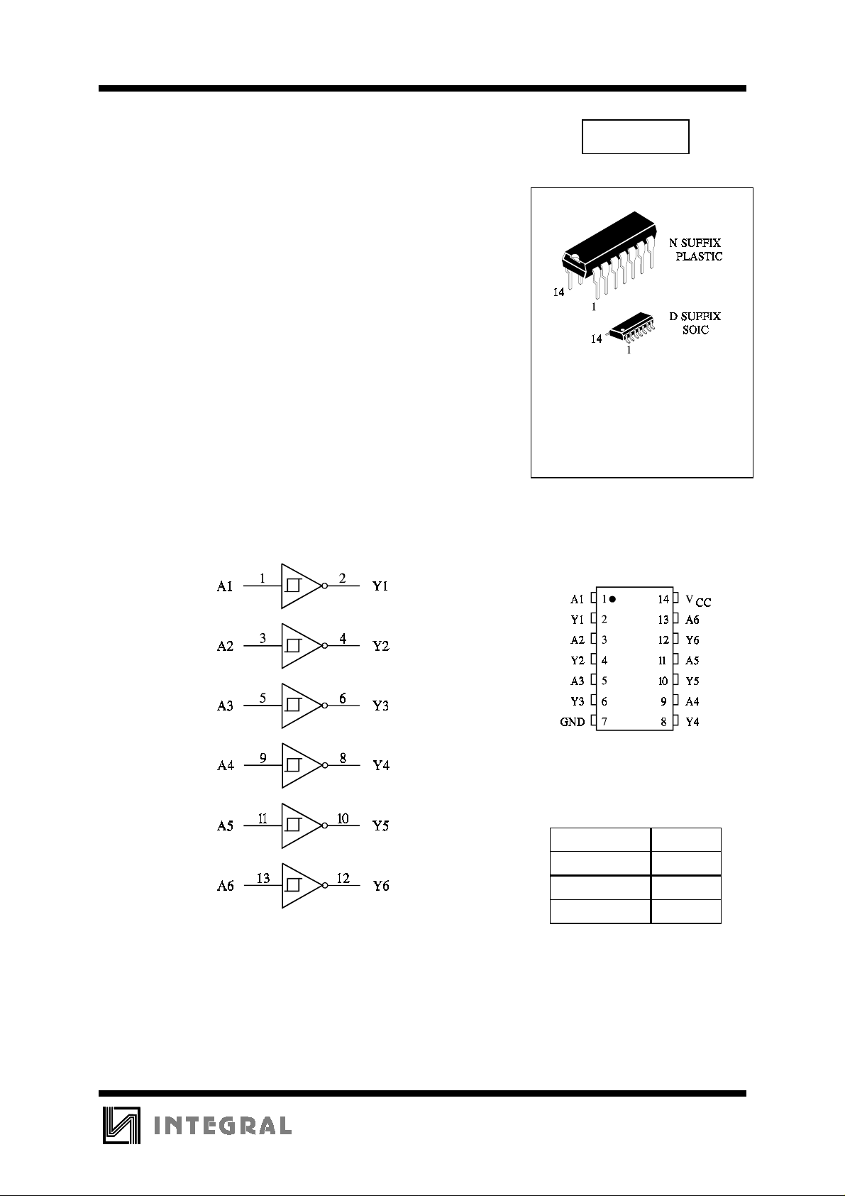
This device contains six independent gates each of which performs
the logic INVERT function. Each input has hysteresis which increases
the noise immunity and transforms a slowly changing input signal to a
fast changing, jitter free output.
TECHNICAL DATA
IN74LS14
ORDERING INFORMATION
IN74LS14N Plastic
IN74LS14D SOIC
TA = 0° to 70° C for all
packages
LOGIC DIAGRAM
PIN ASSIGNMENT
FUNCTION TABLE
Inputs Output
AY
LH
HL
PIN 14 =V
PIN 7 = GND
CC
1
IN74LS14
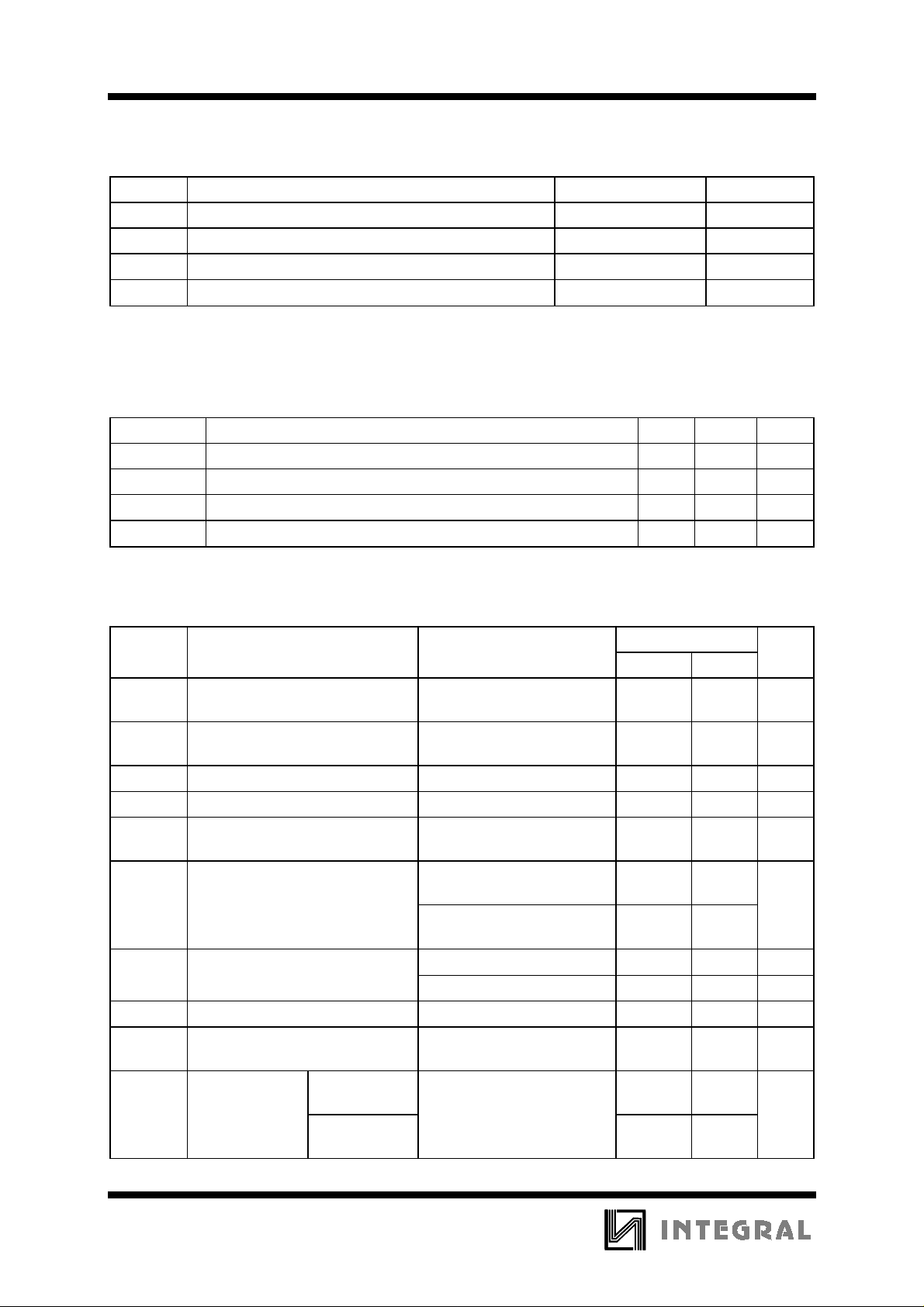
MAXIMUM RATINGS
*
Symbol Parameter Value Unit
V
CC
V
V
OUT
Supply Voltage 7.0 V
Input Voltage 7.0 V
IN
Output Voltage 5.5 V
Tstg Storage Temperature Range -65 to +150
*
Maximum Ratings are those values beyond which damage to the device may occur.
Functional operation should be restricted to the Recommended Operating Conditions.
RECOMMENDED OPERATING CONDITIONS
Symbol Parameter Min Max Unit
V
CC
I
OH
I
OL
T
A
Supply Voltage 4.75 5.25 V
High Level Output Current -15 mA
Low Level Output Current 24 mA
Ambient Temperature Range 0 +70
°
C
°
C
DC ELECTRICAL CHARACTERISTICS
over full operating conditions
Guaranteed Limit
Symbol Parameter Test Conditions Min Max Unit
VT+
Positive-Going Input Threshold
-
VCC = 5 V 0.5 1 V
Voltage
VT-
Negative-Going Input Threshold
-
VCC = 5 V 1.4 1.9 V
Voltage
VT+ - VT-Hysteresis VCC = 5 V 0.4 V
V
V
OH
V
OL
I
IH
Input Clamp Voltage VCC = min, IIN = -18 mA -1.5 V
IK
High Level Output Voltage VCC = min, IOH = -0.4 mA,
V
=0.5 V
I
Low Level Output Voltage VCC = min, IOL = 4 mA
V
=1.9 V
I
VCC = min, IOL = 8 mA
V
=1.9 V
I
High Level Input Current VCC = max, VIN = 2.7 V 20
2.7 V
0.4 V
0.5
µ
VCC = max, VIN = 7.0 V 0.1 mA
I
IL
I
O
Low Level Input Current VCC = max, VIN = 0.4 V -0.4 mA
Output Short Circuit Current VCC = max, VO =0 V
-20 -100 mA
(Note 1)
I
CC
Supply Current Total with
VCC = max 16 mA
outputs high
Total with
21
outputs low
Note 1: Not more than one output should be shorted at a time, and the duration should not exceed one second.
A
2
 Loading...