INTEGRAL IN74LS138D, IN74LS138N Datasheet

3-to-8-Line Decoder/Demultiplexer
This schottky-clamped TTL MSI circuit is designed to be used in
high-performance memory-decording or data-routing applications
requiring very short propagation delay time. In high-performance
memory systems this decode can be used to minimize the effects of
system decoding. When employed with high-speed memories utilizing
a fast enable circuit the delay times of this decorder and the enable
time of the memory are usually less than the typical access times of the
memory. This means that the effective system delay introduced by the
schottky-clampled system decoder is negligible.
•
Designed Specifically for High Speed Memory Decoders and Data
Transmission Systems
•
Incorporate 3 Enabler Inputs to Simplify Cascading AND/OR Data
Reception
•
Schottky Clamped for High Performance
TECHNICAL DATA
IN74LS138
ORDERING INFORMATION
IN74LS138N Plastic
IN74LS138D SOIC
TA = 0° to 70° C
for all packages
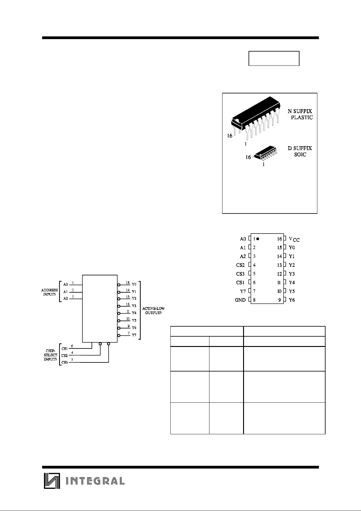
LOGIC DIAGRAM
PIN 16 =V
PIN 8 = GND
CC
PIN ASSIGNMENT
FUNCTION TABLE
Inputs Outputs
CS1 CS2 CS3 A2 A1 A0 Y0 Y1 Y2 Y3 Y4 Y5 Y6 Y7
X X H
X H X
L X X
H L L
H L L
H L L
H L L
H L L
H L L
H L L
H L L
H = high level (ste ady state)
L = low level (steady state)
X = don’t care
X X X
X X X
X X X
L L L
L L H
L H L
L H H
H L L
H L H
H H L
H H H
H H H H H H H H
H H H H H H H H
H H H H H H H H
L H H H H H H H
H L H H H H H H
H H L H H H H H
H H H L H H H H
H H H H L H H H
H H H H H L H H
H H H H H H L H
H H H H H H H L
1

IN74LS138
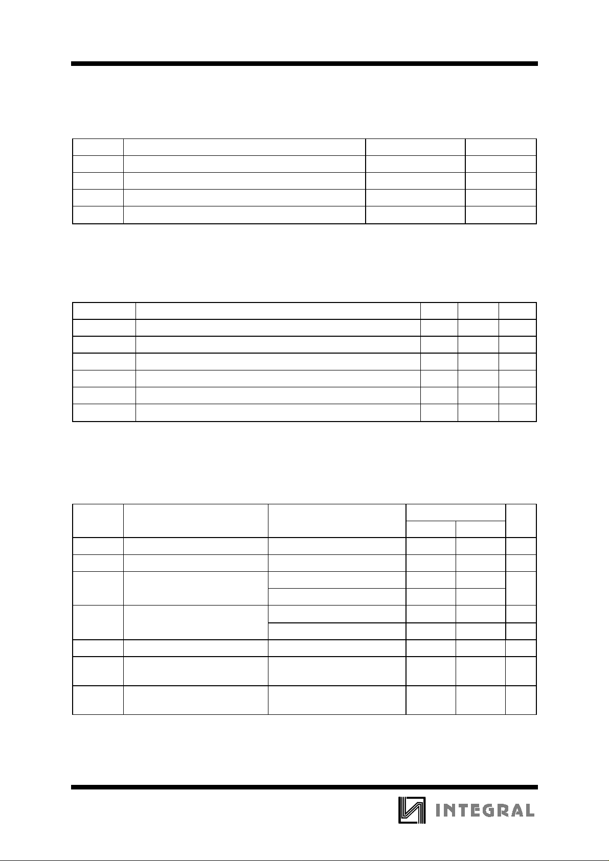
MAXIMUM RATINGS
*
Symbol Parameter Value Unit
V
CC
V
V
OUT
Supply Voltage 7.0 V
Input Voltage 7.0 V
IN
Output Voltage 5.5 V
Tstg Storage Temperature Range -65 to +150
*
Maximum Ratings are those values beyond which damage to the device may occur.
Functional operation should be restricted to the Recommended Operating Conditions.
RECOMMENDED OPERATING CONDITIONS
Symbol Parameter Min Max Unit
V
CC
V
IH
V
IL
I
OH
I
OL
T
A
Supply Voltage 4.75 5.25 V
High Level Input Voltage 2.0 V
Low Level Input Voltage 0.8 V
High Level Output Current -0.4 mA
Low Level Output Current 8.0 mA
Ambient Temperature Range 0 +70
°
C
°
C
DC ELECTRICAL CHARACTERISTICS
over full operating conditions
Guaranteed Limit
Symbol Parameter Test Conditions Min Max Unit
V
V
OH
V
OL
Input Clamp Voltage VCC = min, IIN = -18 mA -1.5 V
IK
High Level Output Voltage VCC = min, IOH = -0.4 mA 2.7 V
Low Level Output Voltage VCC = min, IOL = 4 mA 0.4 V
VCC = min, IOL = 8 mA 0.5
I
IH
High Level Input Current VCC = max, VIN = 2.7 V 20
µ
A
VCC = max, VIN = 7.0 V 0.1 mA
I
IL
I
O
Low Level Input Current VCC = max, VIN = 0.4 V -0.4 mA
Output Short Circuit Current VCC = max, VO = 0 V
-20 -100 mA
(Note 1)
I
CC
Supply Current VCC = max
10 mA
Outputs enabled and open
Note 1: Not more than one output should be shorted at a time, and duration should not exceed one second.
2
 Loading...