

INTEGRAL IN74HC597D, IN74HC597N Datasheet
TECHNICAL DATA
432
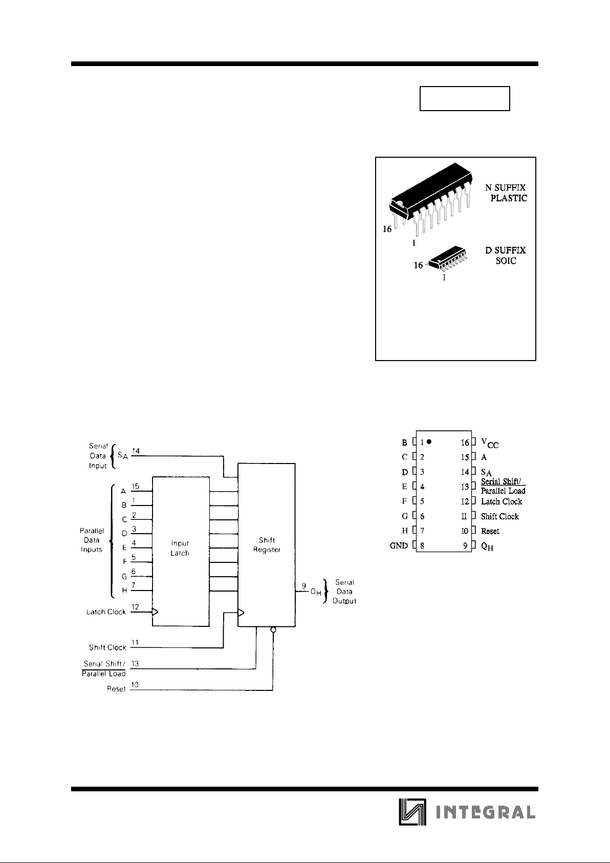
8-Bit Serial or Parallel-Input/
Serial-Output Shift Register
with Input Latch
High-Performance Silicon-Gate CMOS
The IN74HC597 is identical in pinout to the LS/ALS597. The
device inputs are compatible with standard CMOS outputs; with pullup
resistors, they are compatible with LS/ALSTTL outputs.
This device consists of an 8-bit input latch which feeds parallel
data to an 8-bit shift register. Data can also be loaded serially (see
Function Tab l e).
•
Outputs Directly Interface to CMOS, NMOS, and TTL
•
Operating Voltage Range: 2.0 to 6.0 V
•
Low Input Current: 1.0 µA
•
High Noise Immunity Characteristic of CMOS Devices
IN74HC597
ORDERING INFORMATION
IN74HC597N Plastic
IN74HC597D SOIC
TA = -55° to 125° C for all packages
PIN ASSIGNMENT
LOGIC DIAGRAM
PIN 16 =V
CC
PIN 8 = GND
IN74HC597
433
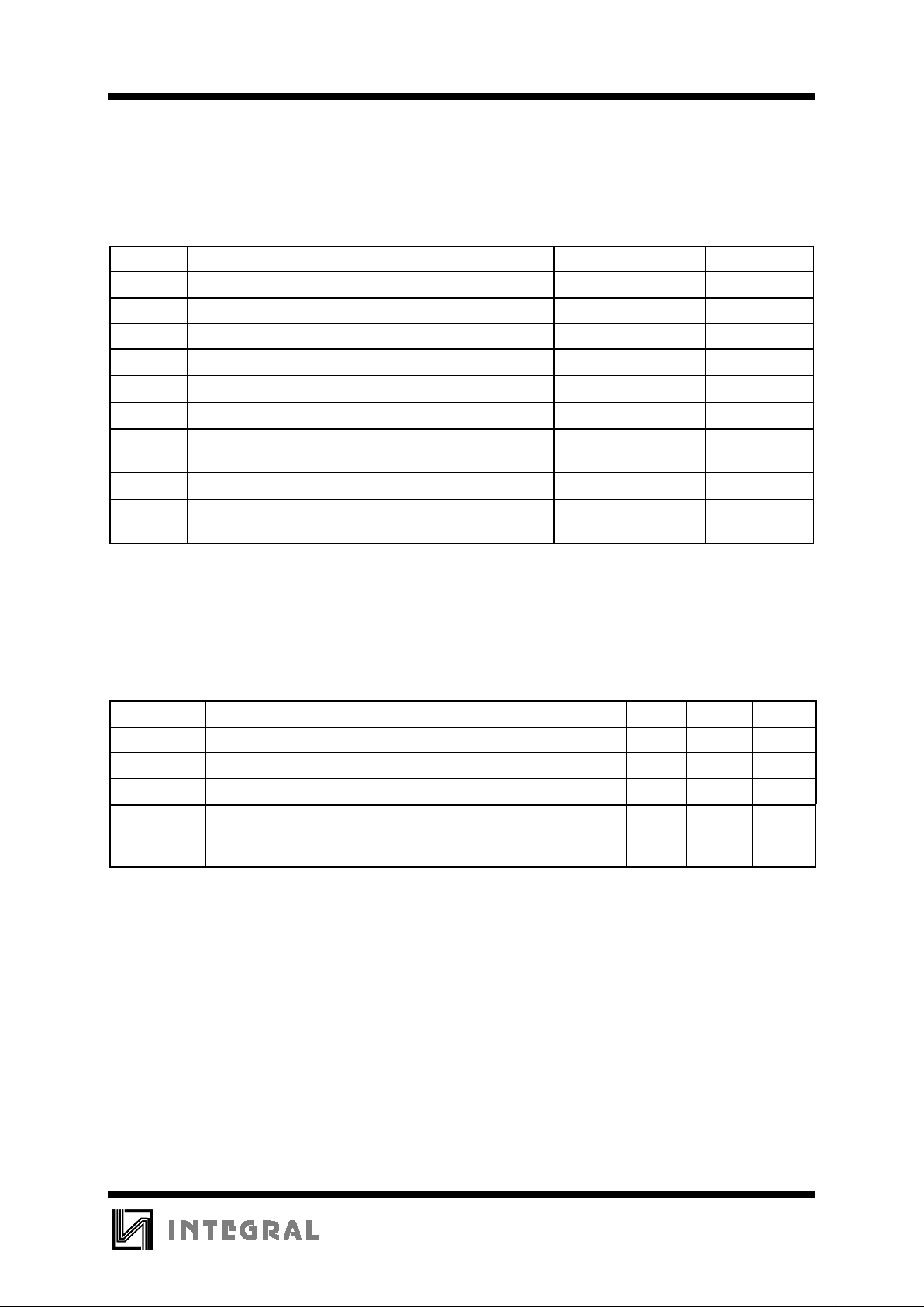
MAXIMUM RATINGS
*
Symbol Parameter Value Unit
V
CC
DC Supply Voltage (Referenced to GND) -0.5 to +7.0 V
V
IN
DC Input Voltage (Referenced to GND) -1.5 to VCC +1.5 V
V
OUT
DC Output Voltage (Referenced to GND) -0.5 to VCC +0.5 V
I
IN
DC Input Current, per Pin
±
20
mA
I
OUT
DC Output Current, per Pin
±
25
mA
I
CC
DC Supply Current, VCC and GND Pins
±
50
mA
P
D
Power Dissipation in Still Air, Plastic DIP+
SOIC Package+
750
500
mW
Tstg Storage Temperature -65 to +150
°
C
T
L
Lead Temperature, 1 mm from Case for 10 Seconds
(Plastic DIP or SOIC Package)
260
°
C
*
Maximum Ratings are those values beyond which damage to the device may occur.
Functional operation should be restricted to the Recommended Operating Conditions.
+Derating - Plastic DIP: - 10 mW/°C from 65° to 125°C
SOIC Package: : - 7 mW/°C from 65° to 125°C
RECOMMENDED OPERATING CONDITIONS
Symbol Parameter Min Max Unit
V
CC
DC Supply Voltage (Referenced to GND) 2.0 6.0 V
VIN, V
OUT
DC Input Voltage, Output Voltage (Referenced to GND) 0 V
CC
V
T
A
Operating Temperature, All Package Types -55 +125
°
C
tr, t
f
Input Rise and Fall Time (Figure 1) VCC =2.0 V
V
CC
=4.5 V
V
CC
=6.0 V
0
0
0
1000
500
400
ns
This device c ontains p rote ction ci rcuitr y to guard a gainst damage d ue to high st atic voltages or electr ic
fields. However, precautions must be taken to avoid applications of any voltage higher than maximum rated
voltages to this high-impedance circuit. For proper operation, V
IN
and V
OUT
should be constrained to the range
GND≤(V
IN
or V
OUT
)≤VCC.
Unused inputs must always be tied to an appropriate logic voltage level (e.g., either GND or V
CC
).
Unused outputs must be left open.
IN74HC597
434
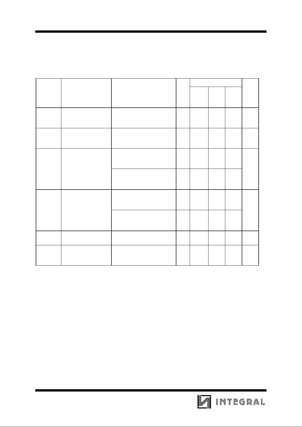
DC ELECTRICAL CHARACTERISTICS
(Voltages Referenced to GND)
V
CC
Guaranteed Limit
Symbol Parameter Test Conditions V
25 °C
to
-55°C
≤
85
°
C
≤
125
°
C
Unit
V
IH
Minimum High-Level
Input Voltage
V
OUT
=0.1 V or VCC-0.1 V
I
OUT
≤
20 µA
2.0
4.5
6.0
1.5
3.15
4.2
1.5
3.15
4.2
1.5
3.15
4.2
V
V
IL
Maximum Low Level Input Voltage
V
OUT
=0.1 V or VCC-0.1 V
I
OUT
≤
20 µA
2.0
4.5
6.0
0.3
0.9
1.2
0.3
0.9
1.2
0.3
0.9
1.2
V
V
OH
Minimum High-Level
Output Voltage
VIN=VIH or V
IL
I
OUT
≤
20 µA
2.0
4.5
6.0
1.9
4.4
5.9
1.9
4.4
5.9
1.9
4.4
5.9
V
VIN=VIH or V
IL
I
OUT
≤
4.0 mA
I
OUT
≤
5.2 mA
4.5
6.0
3.98
5.48
3.84
5.34
3.7
5.2
V
OL
Maximum Low-Leve l
Output Voltage
VIN=VIH or V
IL
I
OUT
≤
20 µA
2.0
4.5
6.0
0.1
0.1
0.1
0.1
0.1
0.1
0.1
0.1
0.1
V
VIN=VIH or V
IL
I
OUT
≤
4.0 mA
I
OUT
≤
5.2 mA
4.5
6.0
0.26
0.26
0.33
0.33
0.4
0.4
I
IN
Maximum Input
Leakage Current
VIN=VCC or GND 6.0
±
0.1
±
1.0
±
1.0
µ
A
I
CC
Maximum Quiesce nt
Supply Current
(per Package)
VIN=VCC or GND
I
OUT
=0µA
6.0 8.0 80 160
µ
A
 Loading...