

INTEGRAL IN74HC595AD Datasheet
8-Bit Serial-Input/Serial or
Parallel-Output Shift Register
with Latched 3-State Outputs
High-Performance Silicon-Gate CMOS
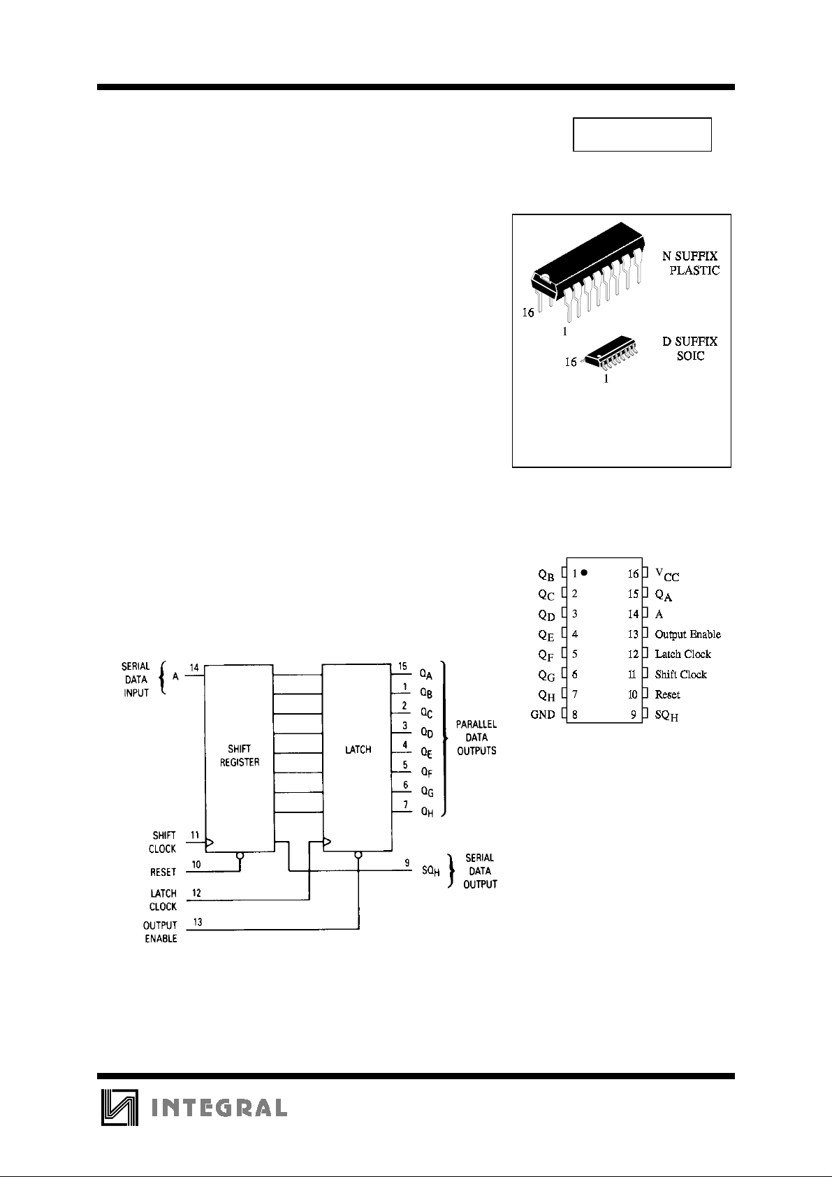
The IN74HC595A is identical in pinout to the LS/ALS595. The
device inputs are compatible with standard CMOS outputs; with pullup
resistors, they are compatible with LS/ALSTTL outputs.
The IN74HC595A consists of an 8-bit shift register and an 8-bit Dtype latch with three-state parallel outputs. The shift register accepts
serial data and provides a serial output. The shift register also provides
parallel data to the 8-bit latch. The shift register and latch have
independent clock inputs. This device also has an asynchronous reset
for the shift register.
•
Outputs Directly Interface to CMOS, NMOS, and TTL
•
Operating Voltage Range: 2.0 to 6.0 V
•
Low Input Current: 1.0 µA
•
High Noise Immunity Characteristic of CMOS Devices
TECHNICAL DATA
IN74HC595A
ORDERING INFORMATION
IN74HC595AN Plastic
IN74HC595AD SOIC
TA = -55° to 125° C for all packages
PIN ASSIGNMENT
LOGIC DIAGRAM
PIN 16 =V
PIN 8 = GND
CC
423
IN74HC595A
MAXIMUM RATINGS
*
Symbol Parameter Value Unit
V
CC
V
V
OUT
I
IN
I
OUT
I
CC
P
DC Supply Voltage (Referenced to GND) -0.5 to +7.0 V
DC Input Voltage (Referenced to GND) -1.5 to VCC +1.5 V
IN
DC Output Voltage (Referenced to GND) -0.5 to VCC +0.5 V
DC Input Current, per Pin
DC Output Current, per Pin
DC Supply Current, VCC and GND Pins
Power Dissipation in Still Air, Plastic DIP+
D
SOIC Package+
±
20
±
35
±
75
750
500
Tstg Storage Temperature -65 to +150
T
Lead Temperature, 1 mm from Case for 10 Seconds
L
260
(Plastic DIP or SOIC Package)
*
Maximum Ratings are those values beyond which damage to the device may occur.
Functional operation should be restricted to the Recommended Operating Conditions.
+Derating - Plastic DIP: - 10 mW/°C from 65° to 125°C
SOIC Package: : - 7 mW/°C from 65° to 125°C
mA
mA
mA
mW
°
C
°
C
RECOMMENDED OPERATING CONDITIONS
Symbol Parameter Min Max Unit
V
CC
VIN, V
T
A
tr, t
f
This device c ontains p rote ction ci rcuitr y to guard a gainst damage d ue to high st atic voltages or electr ic
fields. However, precautions must be taken to avoid applications of any voltage higher than maximum rated
voltages to this high-impedance circuit. For proper operation, V
GND≤(V
Unused inputs must always be tied to an appropriate logic voltage level (e.g., either GND or V
Unused outputs must be left open.
DC Supply Voltage (Referenced to GND) 2.0 6.0 V
DC Input Voltage, Output Voltage (Referenced to GND) 0 V
OUT
Operating Temperature, All Package Types -55 +125
Input Rise and Fall Time (Figure 1) VCC =2.0 V
IN
or V
OUT
)≤VCC.
V
CC
V
CC
and V
IN
=4.5 V
=6.0 V
OUT
should be constrained to the range
0
0
0
CC
1000
500
400
V
°
C
ns
CC
).
424
IN74HC595A
DC ELECTRICAL CHARACTERISTICS
(Voltages Referenced to GND)
Symbol Parameter Test Conditions V
V
V
V
OH
V
OL
V
OH
V
OL
I
IN
Minimum High-Level
IH
Input Voltage
Maximum Low -
IL
Level Input Voltage
Minimum High-Level
Output Voltage, Q
Q
H
Maximum Low-Level
Output Voltage, Q
Q
H
Minimum High-Level
Output Voltage, SQ
Maximum Low-Level
Output Voltage, SQ
Maximum Input
V
=0.1 V or VCC-0.1 V
OUT
≤
I
20 µA
OUT
V
=0.1 V or VCC-0.1 V
OUT
≤
I
20 µA
OUT
-
A
-
A
H
H
VIN=VIH or V
≤
I
OUT
VIN=VIH or V
≤
I
OUT
≤
I
OUT
VIN=VIH or V
≤
I
OUT
VIN=VIH or V
≤
I
OUT
≤
I
OUT
VIN=VIH or V
≤
I
OUT
VIN=VIH or V
≤
I
OUT
≤
I
OUT
VIN=VIH or V
≤
I
OUT
VIN=VIH or V
≤
I
OUT
≤
I
OUT
IL
20 µA
IL
6.0 mA
7.8 mA
IL
20 µA
IL
6.0 mA
7.8 mA
IL
20 µA
IL
4.0 mA
5.2 mA
IL
20 µA
IL
4.0 mA
5.2 mA
VIN=VCC or GND 6.0
Leakage Current
I
OZ
Maximum ThreeState Leakage
Current, Q
A-QH
Output in High-Impedance
State
V
= VIL or V
IN
IH
VIN=VCC or GND
I
CC
Maximum Quiescent
Supply Current
VIN=VCC or GND
=0µA
I
OUT
(per Package)
V
CC
Guaranteed Limit
25 °C
to
≤
85
°
C
≤
125
°
-55°C
2.0
4.5
6.0
2.0
4.5
6.0
2.0
4.5
6.0
4.5
6.0
2.0
4.5
6.0
4.5
6.0
2.0
4.5
6.0
4.5
6.0
2.0
4.5
6.0
4.5
6.0
6.0
1.5
3.15
4.2
0.5
1.35
1.8
1.9
4.4
5.9
3.98
5.48
0.1
0.1
0.1
0.26
0.26
1.9
4.4
5.9
3.98
5.48
0.1
0.1
0.1
0.26
0.26
±
0.1
±
0.5
1.5
3.15
4.2
0.5
1.35
1.8
1.9
4.4
5.9
3.84
5.34
0.1
0.1
0.1
0.33
0.33
1.9
4.4
5.9
3.84
5.34
0.1
0.1
0.1
0.33
0.33
±
1.0
±
5.0
1.5
3.15
4.2
0.5
1.35
1.8
1.9
4.4
5.9
3.7
5.2
0.1
0.1
0.1
0.4
0.4
1.9
4.4
5.9
3.7
5.2
0.1
0.1
0.1
0.4
0.4
±
±
6.0 4.0 40 160
C
1.0
10
Unit
V
V
V
V
V
V
µ
A
µ
A
µ
A
425
 Loading...