

INTEGRAL IN74HC4094N, IN74HC4094D Datasheet
8-Bit Serial-Input Shift Register
With Latched 3-State Outputs
High-Performance Silicon-Gate CMOS
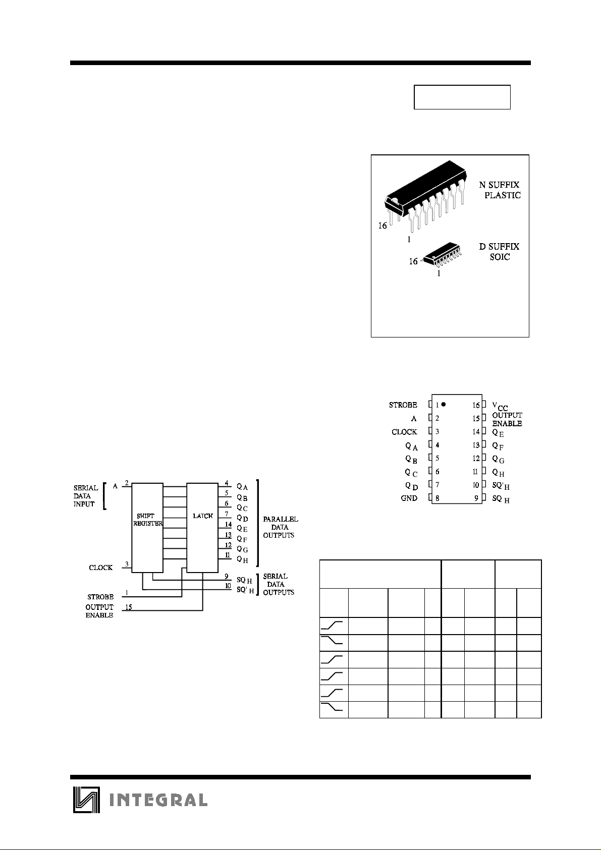
The IN74HC4094 is identical in pinout to the LS/ALS4094. The
device inputs are compatible with standard CMOS outputs; with pullup
resistors, they are compatible with LS/ALSTTL outputs.
This device consists of an 8-bit shift register and 8-bit D-type latch
with three-state parallel outputs. Data is shifted serially through the
shift register on the positive going transition of the clock input signal.
The output of the last stage SQ
devices.
Data on the SQ
the following negative transition of the clock input signal. The data of
each stage of the shift register is provided with a latch, which latches
data on the negative going transition of the Strobe input signal. When
the Strobe inp ut is held high, d ata pro pagates through the latch to a 3 state output buffer.
This buffer is enabled when Output Enable input is taken high.
•
Outputs Directly Interface to CMOS, NMOS, and TTL
•
Operating Voltage Range: 2.0 to 6.0 V
•
Low Input Current: 1.0 µA
•
High Noise Immunity Characteristic of CMOS Devices
output is transferred to a second output (SQH’) on
H
can be used to cascade several
H
TECHNICAL DATA
IN74HC4094
ORDERING INFORMATION
IN74HC4094N Plastic
IN74HC4094D SOIC
TA = -55° to 125° C for all packages
PIN ASSIGNMENT
LOGIC DIAGRAM
PIN 16 =V
PIN 8 = GND
CC
FUNCTION TABLE
Inputs Parallel
Clock Output
Enable
LXXZZQ6NC
LXXZZNCSQ
HLXNCNCQ6NC
HHLLQ
HHHHQ
HXXNCNCNCSQ
NC = No Change
Z = high impedance
X = don’t care
Serial
Outputs
Strobe A QAQNSQHSQH’
N-1
N-1
Outputs
Q6 NC
Q6 NC
H
H
515
IN74HC4094
MAXIMUM RATINGS
*
Symbol Parameter Value Unit
V
CC
V
V
OUT
I
IN
I
OUT
I
CC
P
DC Supply Voltage (Referenced to GND) -0.5 to +7.0 V
DC Input Voltage (Referenced to GND) -1.5 to VCC +1.5 V
IN
DC Output Voltage (Referenced to GND) -0.5 to VCC +0.5 V
DC Input Current, per Pin
DC Output Current, per Pin
DC Supply Current, VCC and GND Pins
Power Dissipation in Still Air, Plastic DIP+
D
SOIC Package+
±
20
±
25
±
50
750
500
Tstg Storage Temperature -65 to +150
T
Lead Temperature, 1 mm from Case for 10 Seconds
L
260
(Plastic DIP or SOIC Package)
*
Maximum Ratings are those values beyond which damage to the device may occur.
Functional operation should be restricted to the Recommended Operating Conditions.
+Derating - Plastic DIP: - 10 mW/°C from 65° to 125°C
SOIC Package: : - 7 mW/°C from 65° to 125°C
mA
mA
mA
mW
°
C
°
C
RECOMMENDED OPERATING CONDITIONS
Symbol Parameter Min Max Unit
V
CC
VIN, V
T
A
tr, t
f
This device c ontains p rote ction ci rcuitr y to guard a gainst damage d ue to high st atic voltages or electr ic
fields. However, precautions must be taken to avoid applications of any voltage higher than maximum rated
voltages to this high-impedance circuit. For proper operation, V
GND≤(V
Unused inputs must always be tied to an appropriate logic voltage level (e.g., either GND or V
Unused outputs must be left open.
DC Supply Voltage (Referenced to GND) 2.0 6.0 V
DC Input Voltage, Output Voltage (Referenced to GND) 0 V
OUT
Operating Temperature, All Package Types -55 +125
Input Rise and Fall Time (Figure 1) VCC =2.0 V
IN
or V
OUT
)≤VCC.
V
V
IN
=4.5 V
CC
=6.0 V
CC
and V
should be constrained to the range
OUT
0
0
0
CC
1000
500
400
°
ns
V
C
CC
).
516
IN74HC4094
DC ELECTRICAL CHARACTERISTICS
(Voltages Referenced to GND)
Symbol Parameter Test Conditions V
V
V
V
OH
V
OL
I
IN
Minimum High-Level
IH
Input Voltage
Maximum Low -
IL
Level Input Voltage
Minimum High-Level
Output Voltage
Maximum Low-Level
Output Voltage
Maximum Input
V
= 0.1 V or VCC-0.1 V
OUT
≤
I
20 µA
OUT
V
=0.1 V or VCC-0.1 V
OUT
≤
I
20 µA
OUT
VIN=VIH or V
≤
I
OUT
VIN= VIH or V
≤
I
OUT
≤
I
OUT
VIN=VIH or V
≤
I
OUT
VIN= VIH or V
≤
I
OUT
≤
I
OUT
IL
20 µA
IL
4.0 mA
5.2 mA
IL
20 µA
IL
4.0 mA
5.2 mA
VIN=VCC or GND 6.0
Leakage Current
I
OZ
I
CC
Maximum ThreeState Leakage
Current
Maximum Qui escent
Supply Current
Output in High-Impedance
State
V
= VIL or V
IN
V
OUT=VCC
IH
or GND
VIN=VCC or GND
=0µA
I
OUT
(per Package)
V
CC
Guaranteed Limit
25 °C
to
≤
85
°
C
≤
125
°
-55°C
2.0
4.5
6.0
2.0
4.5
6.0
2.0
4.5
6.0
4.5
6.0
2.0
4.5
6.0
4.5
6.0
6.0
1.5
3.15
4.2
0.5
1.35
1.8
1.9
4.4
5.9
3.98
5.48
0.1
0.1
0.1
0.26
0.26
±
0.1
±
0.5
1.5
3.15
4.2
0.5
1.35
1.8
1.9
4.4
5.9
3.84
5.34
0.1
0.1
0.1
0.33
0.33
±
1.0
±
5.0
1.5
3.15
4.2
0.5
1.35
1.8
1.9
4.4
5.9
3.7
5.2
0.1
0.1
0.1
0.4
0.4
±
±
6.0 4.0 40 160
C
1.0
10
Unit
V
V
V
V
µ
A
µ
A
µ
A
517
 Loading...