

INTEGRAL IN74HC30AN, IN74HC30AD, IN74HC30A Datasheet
8-Input NAND Gate
The IN74HC30A is high-speed Si-gate CMOS device and is
compatible with low power Schottky TTL (LSTTL) . The device
provide the 8-input NAND function.
•
Outputs Directly Interface to CMOS, NMOS, and TTL
•
Operating Voltage Range: 2.0 to 6.0 V
•
Low Input Current: 1.0 µA
•
High Noise Immunity Characteristic of CMOS Devices
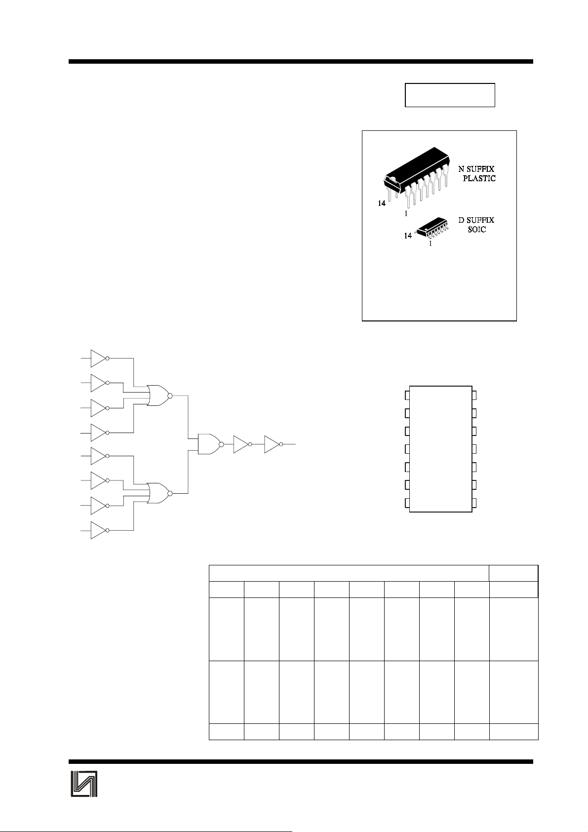
LOGIC DIAGRAM
TECHNICAL DATA
IN74HC30A
ORDERING INFORMATION
IN74HC30AN Plastic
IN74HC30AD SOIC
IZ74HC30A Chip
TA = -55° ÷ 125° C for all packages
A
PIN ASSIGNMENT
B
1
A
C
D
Y
E
F
G
H
GND
2
B
C
3
4
D
5
E
F
6
7
14
13
12
11
10
9
8
V
CC
-
H
G
-.
-
Y
FUNCTION TABLE
PIN 14 =V
PIN 7 = GND
CC
Inputs Output
ABС DEFGH Y
LXXXXXXX H
XL XXXXXX H
XXLXXXXX H
XXXLXXXX H
XXXXLXXX H
XXXXXLXX H
XXXXXXLX H
XXXXXXXL H
HHHHHHHH L
INTEGRAL
X = don’t care
1
IN74HC30A
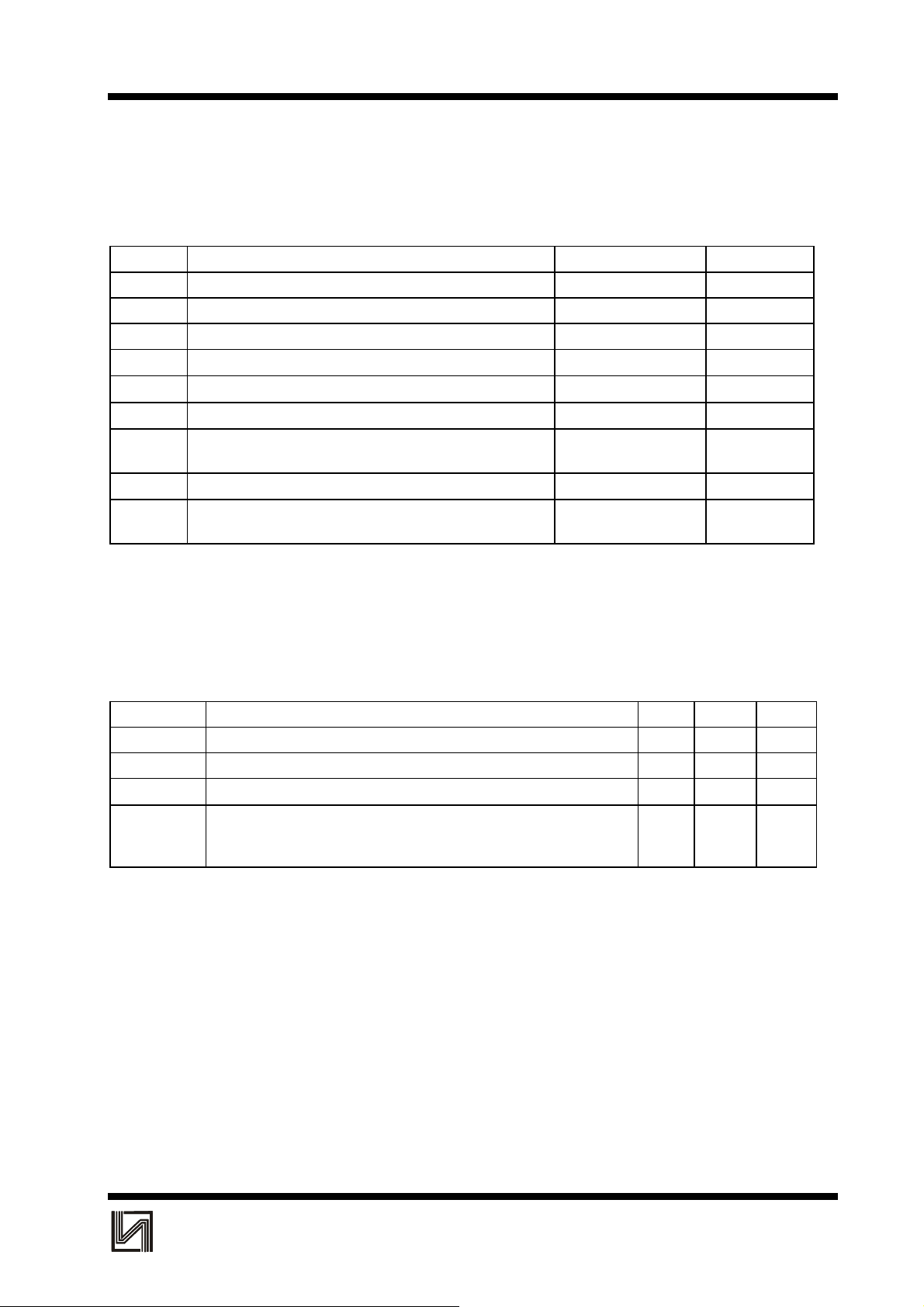
MAXIMUM RATINGS
*
Symbol Parameter Value Unit
V
CC
V
V
OUT
I
IN
I
OUT
I
CC
P
DC Supply Voltage (Referenced to GND) -0.5 to +7.0 V
DC Input Voltage (Referenced to GND) -1.5 to VCC +1.5 V
IN
DC Output Voltage (Referenced to GND) -0.5 to VCC +0.5 V
DC Input Current, per Pin
DC Output Current, per Pin
DC Supply Current, VCC and GND Pins
Power Dissipation in Still Air, Plastic DIP**
D
SOIC Package**
±
20
±
25
±
50
750
500
Tstg Storage Temperature -65 to +150
T
Lead Temperature, 1 mm from Case for 10 Seconds
L
260
(Plastic DIP or SOIC Package)
*Maximum Ratings are those values beyond which damage to the device may occur.
Functional operation should be restricted to the Recommended Operating Conditions.
**Derating - Plastic DIP: - 10 mW/°C from 65° to 125°C
SOIC Package: : - 7 mW/°C from 65° to 125°C
mA
mA
mA
mW
°
C
°
C
RECOMMENDED OPERATING CONDITIONS
Symbol Parameter Min Max Unit
V
CC
VIN, V
OUT
T
A
tr, t
f
This device contains protection circuitry to guard against damage due to high static voltages or electric
fields. However, precautions must be taken to avoid applications of any voltage higher than maximum rated voltages
to this high-impedance circuit. For proper operation, V
)≤VCC.
V
OUT
Unused inputs must always be tied to an appropriate logic voltage level (e.g., either GND or V
outputs must be left open.
DC Supply Voltage (Referenced to GND) 2.0 6.0 V
DC Input Voltage, Output Voltage (Referenced to GND) 0 V
Operating Temperature, All Package Types -55 +125
Input Rise and Fall Time (Figure 1) VCC =2.0 V
V
=4.5 V
CC
V
=6.0 V
CC
and V
IN
should be constrained to the range GND≤(VIN or
OUT
0
0
0
CC
1000
500
400
°
ns
). Unused
CC
V
C
INTEGRAL
2
 Loading...