

INTEGRAL IN74HC166N Datasheet
8-Bit Serial or Parallel-Input/
Serial-Output Shift Register
High-Performance Silicon-Gate CMOS
The IN74HC166 is identical in pinout to the LS/ALS166. The
device inputs are compatible with standard CMOS outputs; with pullup
resistors, they are compatible with LS/ALSTTL outputs.
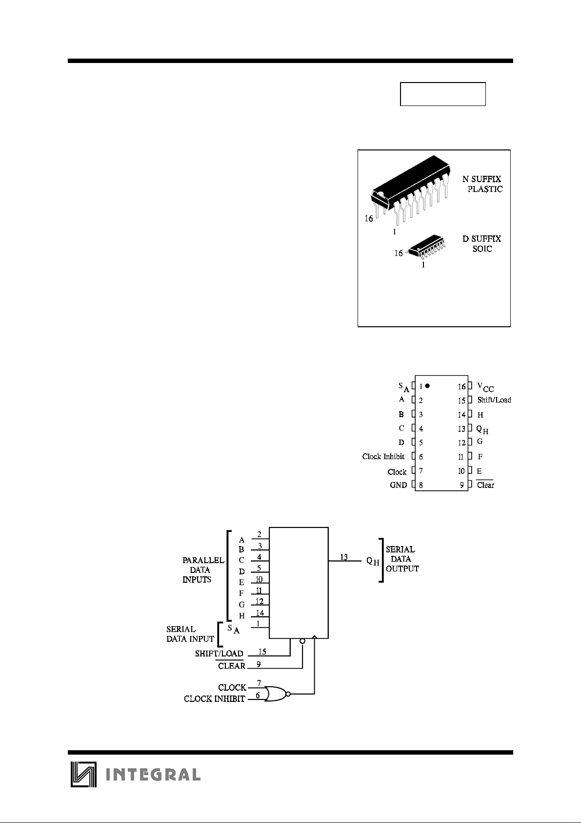
This device is a parallel-in or serial-in, serial-out shift register with
gated clock inputs and an overriding clear input. The shift/load input
establishes the parallel-in or serial-in mode. When high, this input
enables the serial data input and couples the eight flip-flops for serial
shifting with each clock pulse. Synchronous loading occurs on the next
clock pulse when this is low and the parallel data inputs are enabled.
Serial data flow is inhibited during parallel loading. Clocking is done
on the low-to-high level edge of the clock pulse via a two input
positive NOR gate, which permits one input to be used as a clock
enable or c lock inhibit function. Clo cking is inhibited when either o f
the clock inputs are held high, holding either input low enables the
other clock input. T his will allow the system clock to b e fr ee r unning
and the register stopped on command with the other clock input. A
change from low-to-high on the clock inhibit input should only be
done when the clock input is high. A buffered direct clear input
overrides all other inputs, including the clock, andsets all flip-flop to
zero.
•
Outputs Directly Interface to CMOS, NMOS, and TTL
•
Operating Voltage Range: 2.0 to 6.0 V
•
Low Input Current: 1.0 µA
•
High Noise Immunity Characteristic of CMOS Devices
TECHNICAL DATA
IN74HC166
ORDERING INFORMATION
IN74HC166N Plastic
IN74HC166D SOIC
TA = -55° to 125° C for all packages
PIN ASSIGNMENT
LOGIC DIAGRAM
PIN 16 =V
PIN 8 = GND
CC
235
IN74HC166
MAXIMUM RATINGS
*
Symbol Parameter Value Unit
V
CC
V
V
OUT
I
IN
I
OUT
I
CC
P
DC Supply Voltage (Referenced to GND) -0.5 to +7.0 V
DC Input Voltage (Referenced to GND) -1.5 to VCC +1.5 V
IN
DC Output Voltage (Referenced to GND) -0.5 to VCC +0.5 V
DC Input Current, per Pin
DC Output Current, per Pin
DC Supply Current, VCC and GND Pins
Power Dissipation in Still Air, Plastic DIP+
D
SOIC Package+
±
20
±
25
±
50
750
500
Tstg Storage Temperature -65 to +150
T
Lead Temperature, 1 mm from Case for 10 Seconds
L
260
(Plastic DIP or SOIC Package)
*
Maximum Ratings are those values beyond which damage to the device may occur.
Functional operation should be restricted to the Recommended Operating Conditions.
+Derating - Plastic DIP: - 10 mW/°C from 65° to 125°C
SOIC Package: : - 7 mW/°C from 65° to 125°C
mA
mA
mA
mW
°
C
°
C
RECOMMENDED OPERATING CONDITIONS
Symbol Parameter Min Max Unit
V
CC
VIN, V
T
A
tr, t
f
This device c ontains p rote ction ci rcuitr y to guard a gainst damage d ue to high st atic voltages or electr ic
fields. However, precautions must be taken to avoid applications of any voltage higher than maximum rated
voltages to this high-impedance circuit. For proper operation, V
GND≤(V
Unused inputs must always be tied to an appropriate logic voltage level (e.g., either GND or V
Unused outputs must be left open.
DC Supply Voltage (Referenced to GND) 2.0 6.0 V
DC Input Voltage, Output Voltage (Referenced to GND) 0 V
OUT
Operating Temperature, All Package Types -55 +125
Input Rise and Fall Time (Figure 1) VCC =2.0 V
IN
or V
OUT
)≤VCC.
V
CC
V
CC
and V
IN
=4.5 V
=6.0 V
OUT
should be constrained to the range
0
0
0
CC
1000
500
400
V
°
C
ns
CC
).
236
 Loading...