

INTEGRAL IN74ALS74D, IN74ALS74N Datasheet
TECHNICAL DATA
1
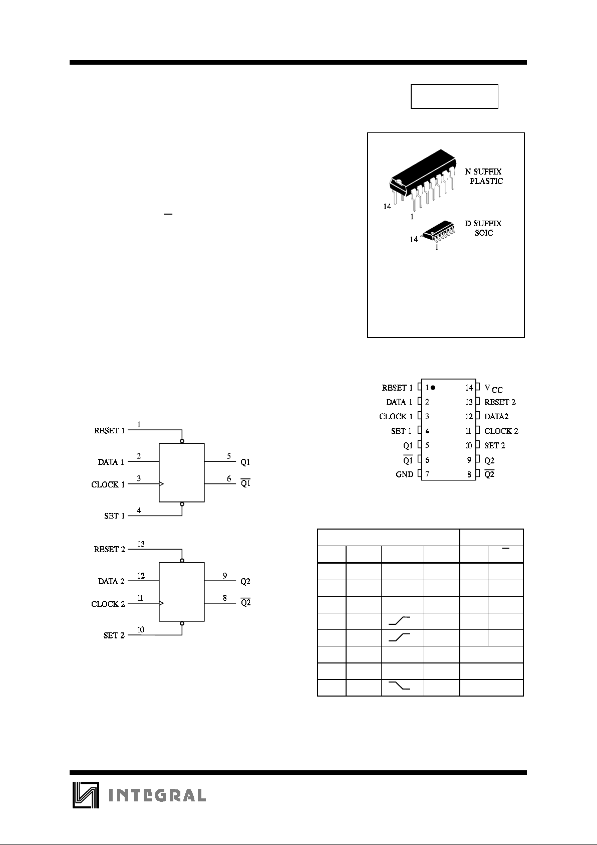
Dual D Flip-Flop with Set and Reset
Each of the two independent positive edge-triggered flip-flops in
this circuit has individual Data, Clock, Set and Reset inputs, and
complementary Q and Q outputs.
•
Switching specificatio ns at 50 pF
•
Switching specifications guaranteed over full temperature and V
CC
range
•
Functionally and pin-for-pin compatible with Schottky and LS TTL
counterpart
•
Improved AC performance over LS74 at approximately half the
power
IN74ALS74
ORDERING INFORMATION
IN74ALS74N Plastic
IN74ALS74D SOIC
TA = -10° to 70° C
for all packages
LOGIC DIAGRAM
PIN 14 =V
CC
PIN 7 = GND
PIN ASSIGNMENT
FUNCTION TABLE
Inputs Outputs
Set Reset Clock Data Q Q
LH X XHL
HL X XLH
LL X XH*H
*
HH HHL
HH LLH
H H L X No Change
H H H X No Change
H H X No Change
*Both outputs will remain high as long as Set
and Reset are low, but the output states are
unpredictable if Set and Reset go hi gh
simultaneously.
X = don’t care
IN74ALS74
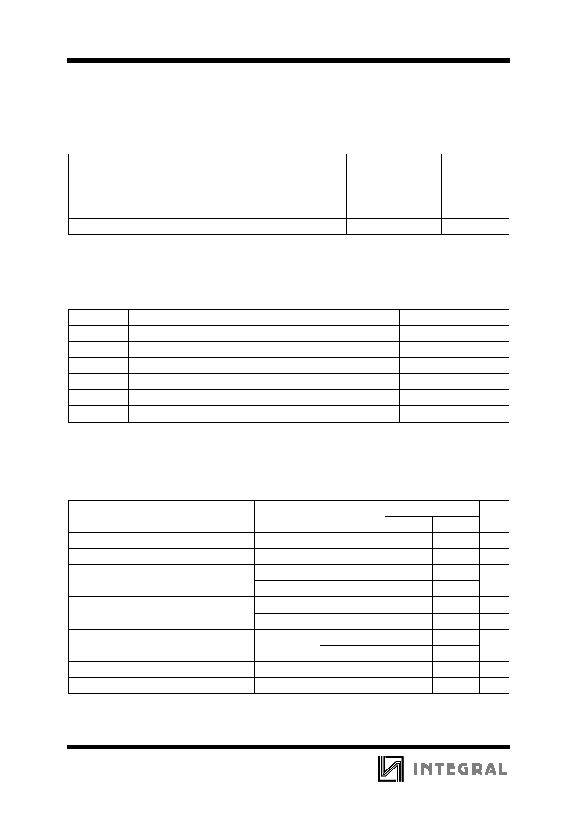
2
MAXIMUM RATINGS
*
Symbol Parameter Value Unit
V
CC
Supply Voltage 7.0 V
V
IN
Input Voltage 7.0 V
V
OUT
Output Voltage 5.5 V
Tstg Storage Temperature Range -65 to +150
°
C
*
Maximum Ratings are those values beyond which damage to the device may occur.
Functional operation should be restricted to the Recommended Operating Conditions.
RECOMMENDED OPERATING CONDITIONS
Symbol Parameter Min Max Unit
V
CC
Supply Voltage 4.5 5.5 V
V
IH
High Level Input Voltage 2.0 V
V
IL
Low Level Input Voltage 0.8 V
I
OH
High Level Output Current -0.4 mA
I
OL
Low Level Output Current 8.0 mA
T
A
Ambient Temperature Range -10 +70
°
C
DC ELECTRICAL CHARACTERISTICS
over full operating conditions
Guaranteed Limit
Symbol Parameter Test Conditions Min Max Unit
V
IK
Input Clamp Voltage VCC = min, IIN = -18 mA -1.5 V
V
OH
High Level Output Voltage VCC = min, IOH = -0.4 mA 2.5 V
V
OL
Low Level Output Voltage VCC = min, IOL = 4 mA 0.4 V
VCC = min, IOL = 8 mA 0.5
I
IH
High Level Input Current VCC = max, VIN = 2.7 V 20
µ
A
VCC = max, VIN = 7.0 V 0.1 mA
I
IL
Low Level Input Current VCC = max, Clock, Dat a -0.2 mA
VIN = 0.4 V Reset, Set -0.4
I
O
Output Short Circuit Current VCC = max, VO = 2.25 V -15 -70 mA
I
CC
Supply Current VCC = max (Note 1) 4.0 mA
Note 1. ICC is measured with Data, Clock and Reset grounded, then with Data, Clock and Set grounded.
 Loading...