

INTEGRAL IN74ALS273N, IN74ALS273DW Datasheet
TECHNICAL DATA
OCTAL D-TYPE FLIP-FLOP WITH CLEAR
• Contains Eight Flip-Flops with Single-Rail Outputs
• Buffered Clock and Direct Clear Inputs
• Individual Data Input to Each Flip-Flop
• Applications Include:
Buffer/Storage Registers
Shift Registers
Pattern Generators
DESCRIPTION
This monolithic, positive-edge-triggered flip-flop
utilizes TTL circuitry to implement D-type flip-flop
logic with a direct clear input.
Information at the D inputs meeting the setup time
requirements is transferred to the Q outputs on the
positive-going edge of the clock pulse. Clock
triggering occurs at a particular voltage level and is not
directly related to the transition time of the positivegoing pulse. When the clock inputs is at either the high
or low level, the D input signal has no effect at the
output.
The IN74ALS273 is characterized for operation from
0oC to 70oC.
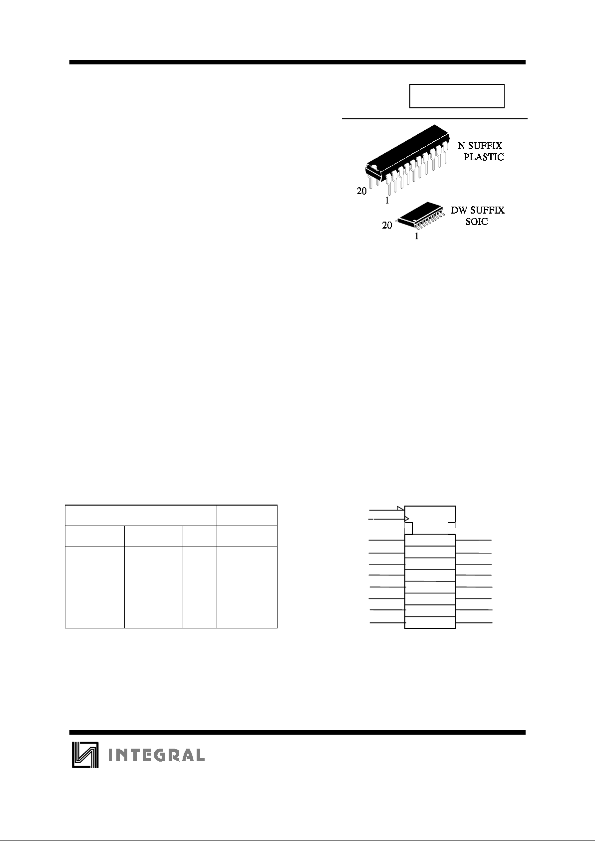
ORDERING INFORMATION
IN74ALS273N Plastic
IN74ALS273DW SOIC
T
A
= 0° to 70° C for all
packages
Function Table and Logic Symbol
(each flip-flop)
INPUTS OUTPUT
CLEAR CLOCK D Q
L
H
H
H
X
I
I
L
X
H
L
X
L
H
L
Q
o
IN74ALS273
CLR
CLK
(1)
(18)
(11)
(3)
(4)
(7)
(17)
(8)
(13)
(14)
(2)
(5)
(6)
(9)
(12)
(15)
(16)
(19)
1D
2D
3D
4D
5D
6D
8Q
7D
8D
7
Q
6Q
5Q
4Q
3
Q
2
Q
1Q
1D
IN74ALS273
2
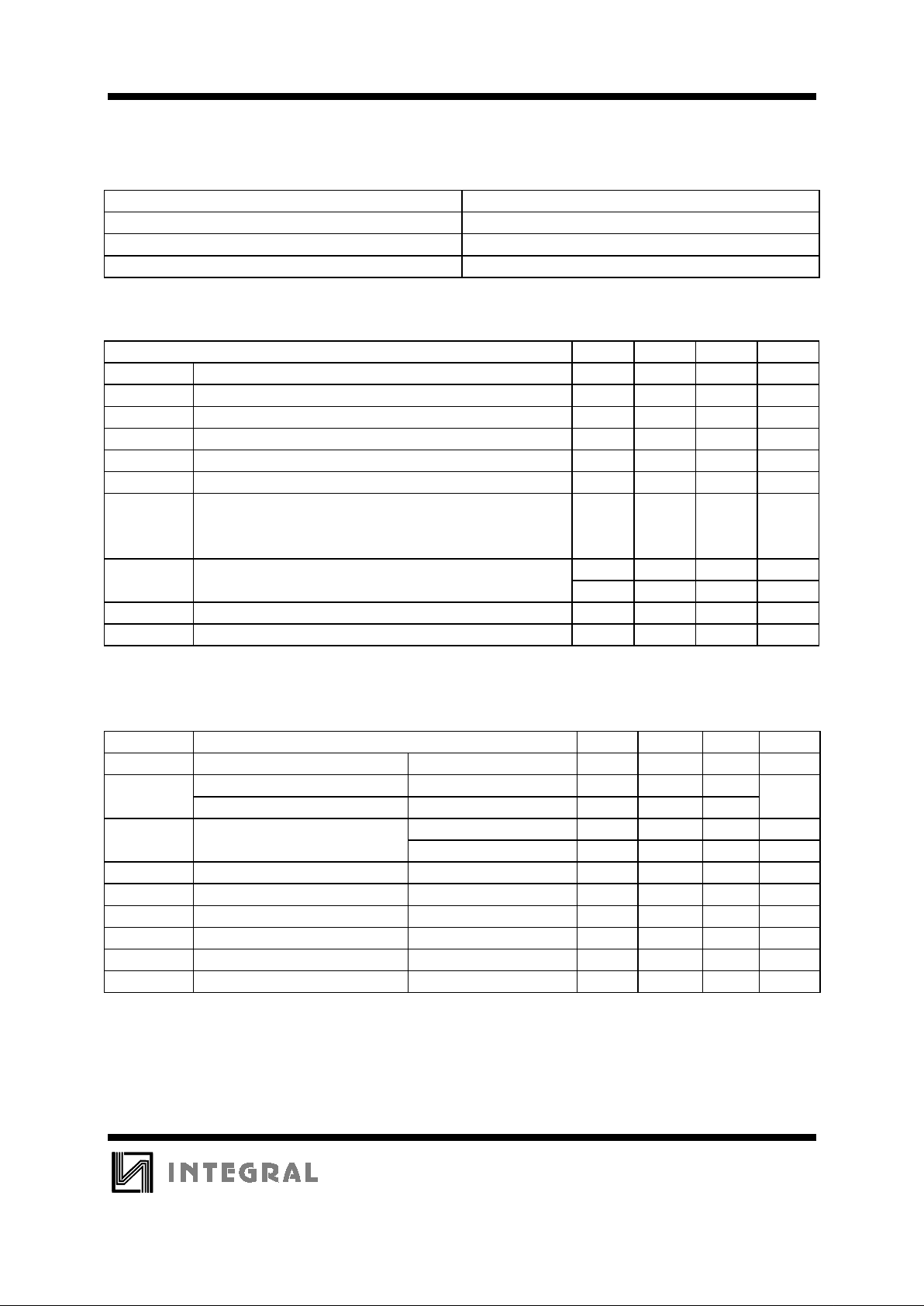
ABSOLUTE MAXIMUM RATINGS OVER OPERATING FREE-AIR
TEMPERATURE RANGE
Supply voltage, Vcc 7V
Input voltage, Vl 7V
Operating free-air temperature range, TA 0oC to 70oC
Storage temperature range-65
o
C to 150oC
RECOMMENDED OPERATING CONDITIONS
MIN NOM MAX UNIT
V
CC
Supply voltage 4.5 5 5.5 V
V
IH
High-level input voltage2V
V
IL
Low-level input voltage 0.8 V
I
OH
High-level output current -2.6 mA
I
OL
Low-level output current 24 mA
f
clock
Clock frequenc
y
035MHz
CLR low 10
t
W
Pulse duration CLK high 14 ns
CLK low 14
t
su
Setup time Data 10 ns
before CLKI Clear inactive state 15 ns
t
l
y
Hold time, data after CLKI 0 ns
T
A
Operating free-air temperature 0 70
o
C
ELECTRICAL CHARACTERISTICS OVER RECOMMENDED OPERATING FREEAIR TEMPERATURE RANGE
Parameter Test Conditions MIN TYP** MAX UNIT
V
IK
VCC= 4.5V II =-18mA -1.5 V
V
OH
VCC= 4.5V to 5.5V IOH =-0.4mA VCC-2 V
VCC= 4.5V IOH =-2.6mA 2.4 3.2
V
OL
VCC= 4.5V IOL =12mA 0.25 0.4 V
IOL =24mA 0.35 0.5 V
I
I
VCC= 5.5V VI =7V 0.1 mA
I
IH
VCC= 5.5V VI =2.7V 20
µ
A
I
IL
VCC= 5.5V VI =0.4V -0.2 mA
IO*V
CC
= 5.5V VO=2.25V -30 -112 mA
I
CCH
VCC= 5.5V 11 20 mA
I
CCL
VCC= 5.5V 19 29 mA
*-The output conditions have been chosen to produce a current that closely approximates one half of the true
short-circuit output current, I
OS
**-All typical values are at VCC=5V, TA=25oC
 Loading...