

INTEGRAL IN74ALS164AN, IN74ALS164AD Datasheet
TECHNICAL DATA
223
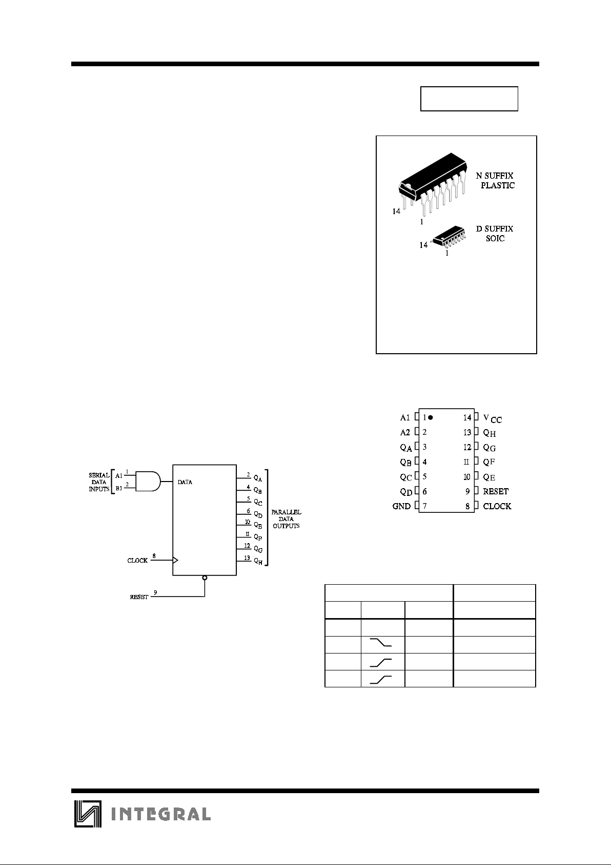
8-Bit Serial-Input/Parallel-Output
Shift Register
This device is a high speed 8-Bit Serial-In-Parallel-Out Shift
Register. Serial data is entered through a 2-Input AND gate
synchronous with the LOW to HIGH transition of the clock. This
device features an asynchronous Master Reset which clears the register
setting all outputs LOW independent of the clock. It utilizes the
Schottky diode clamped process to achieved high speeds and is fully
compatible with all TTL products.
•
Switching specificatio ns at 50 pF
•
Switching specifications guaranteed over full temperature and V
CC
range
•
Functionally and pin-for-pin compatible with Schottky and LS TTL
counterpart
IN74ALS164
ORDERING INFORMATION
IN74ALS164N Plastic
IN74ALS164D SOIC
TA = -10° to 70°C
for all packages
PIN ASSIGNMENT
FUNCTION TABLE
Inputs Outputs
Reset Clock A1 A2 QA QB ... Q
H
L X X X L L ... L
H X X no change
H H D D QAn ... Q
Gn
H D H D QAn ... Q
Gn
D = data input
X = don’t care
Q
An
- Q
Gn
= data shifted from the previous stage on a
rising edge at the clock input.
LOGIC DIAGRAM
PIN 14 =V
CC
PIN 7 = GND
IN74ALS164
224
MAXIMUM RATINGS
*
Symbol Parameter Value Unit
V
CC
Supply Voltage 7.0 V
V
IN
Input Voltage 7.0 V
V
OUT
Output Voltage 5.5 V
Tstg Storage Temperature Range -65 to +150
°
C
*
Maximum Ratings are those values beyond which damage to the device may occur.
Functional operation should be restricted to the Recommended Operating Conditions.
RECOMMENDED OPERATING CONDITIONS
Symbol Parameter Min Max Unit
V
CC
Supply Voltage 4.5 5.5 V
V
IH
High Level Input Voltage 2.0 V
V
IL
Low Level Input Voltage 0.8 V
I
OH
High Level Output Current -0.4 mA
I
OL
Low Level Output Current 8.0 mA
T
A
Ambient Temperature Range -10 +70
°
C
DC ELECTRICAL CHARACTERISTICS
over full operating conditions
Guaranteed Limit
Symbol Parameter Test Conditions Min Max Unit
V
IK
Input Clamp Voltage VCC = min, IIN = -18 mA -1.5 V
V
OH
High Level Output Voltage VCC = min, IOH = -0.4 mA 2.5 V
V
OL
Low Level Output Voltage VCC = min, IOL = 4 mA 0.4 V
VCC = min, IOL = 8 mA 0.5
I
IH
High Level Input Current VCC = max, VIN = 2.7 V 20
µ
A
VCC = max, VIN = 7.0 V 0.1 mA
I
IL
Low Level Input Current VCC = max, VIN = 0.4 V -0.1 mA
I
O
Output Short Circuit Current VCC = max, VO = 2.25 V -30 -112 mA
I
CC
Supply Current VCC = max 24 mA
 Loading...