

INTEGRAL IN74AC574N, IN74AC574DW Datasheet
TECHNICAL DATA
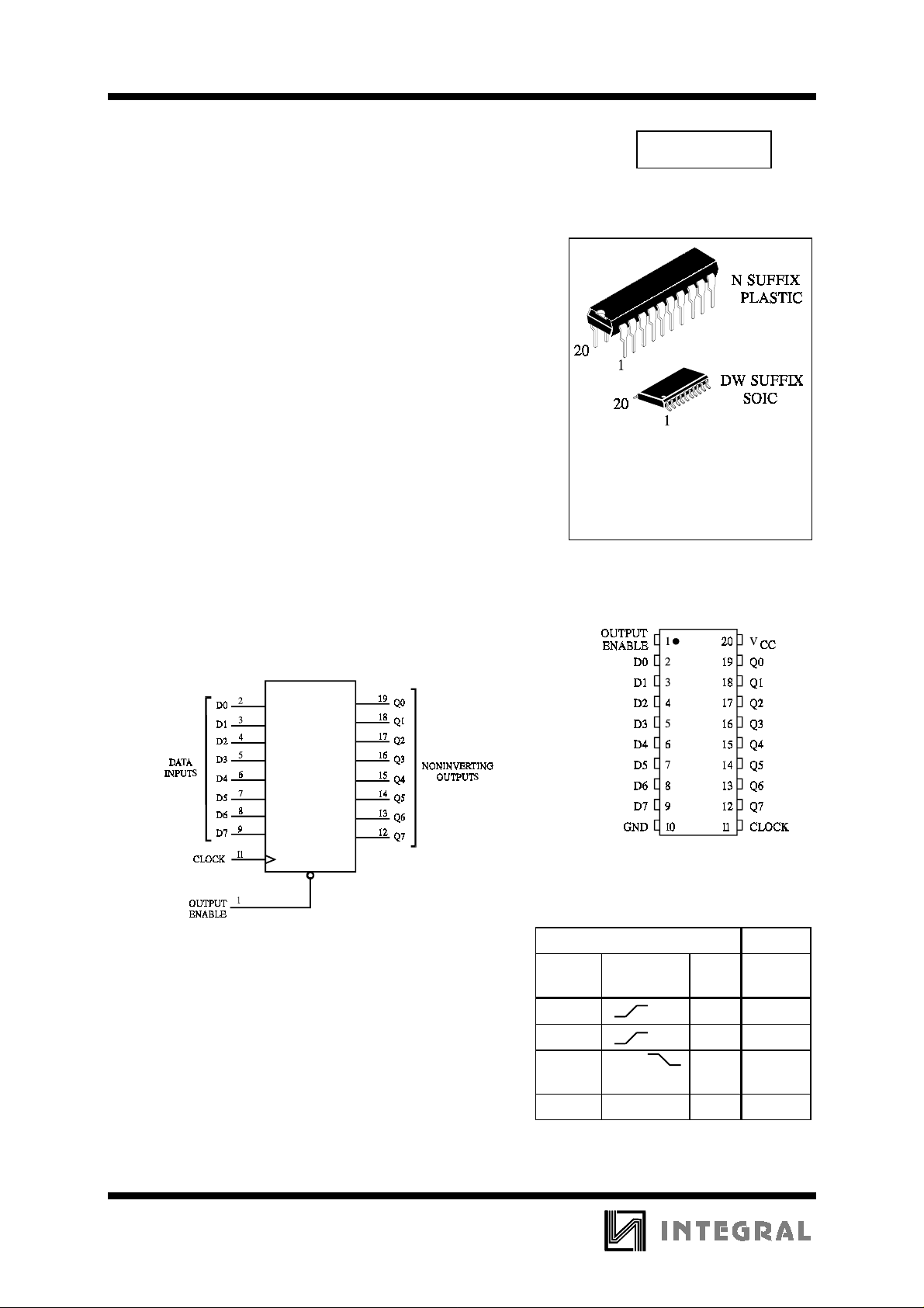
Octal 3-State
Noninverting D Flip-Flop
High-Performance Silicon-Gate CMOS
The IN74AC574 is identical in pinout to the LS/ALS574,
HC/HCT574. The device inputs are compatible with standard CMOS
outputs; with pullup resistors, they are compatible with LS/ALS
outputs.
Data meeting the setup time is clocked to the outputs with the
rising edge of the Clock. The Output Enable input does not affect the
states of the flip-flops, but when Output Enable is high, all device
outputs are forced to the high-impedance state; thus, data may be
stored even when the outputs are not enabled.
•
Outputs Directly Interface to CMOS, NMOS, and TTL
•
Operating Voltage Range: 2.0 to 6.0 V
•
Low Input Current: 1.0 µA; 0.1 µA @ 25°C
•
High Noise Immunity Characteristic of CMOS Devices
•
Outputs Source/Sink 24 mA
IN74AC574
ORDERING INFORMATION
IN74AC574N Plastic
IN74AC574DW SOIC
TA = -40° to 85° C for all
packages
LOGIC DIAGRAM
PIN 20=V
PIN 10 = GND
CC
PIN ASSIGNMENT
FUNCTION TABLE
Inputs Output
Output
Enable
LHH
LLL
LL,H, X no
HXXZ
X = don’t care
Z = high impedance
Clock D Q
change
466
IN74AC574
MAXIMUM RATINGS
*
Symbol Parameter Value Unit
V
CC
V
V
OUT
I
IN
I
OUT
I
CC
P
DC Supply Voltage (Referenced to GND) -0.5 to +7.0 V
DC Input Voltage (Referenced to GND) -0.5 to VCC +0.5 V
IN
DC Output Voltage (Referenced to GND) -0.5 to VCC +0.5 V
DC Input Current, per Pin
DC Output Sink/Source Current, per Pin
DC Supply Current, VCC and GND Pins
Power Dissipation in Still Air, Plastic DIP+
D
SOIC Package+
±
20
±
50
±
50
750
500
Tstg Storage Temperature -65 to +150
T
Lead Temperature, 1 mm from Case for 10 Seconds
L
260
(Plastic DIP or SOIC Package)
*
Maximum Ratings are those values beyond which damage to the device may occur.
Functional operation should be restricted to the Recommended Operating Conditions.
+Derating - Plastic DIP: - 10 mW/°C from 65° to 125°C
SOIC Package: : - 7 mW/°C from 65° to 125°C
mA
mA
mA
mW
°
C
°
C
RECOMMENDED OPERATING CONDITIONS
Symbol Parameter Min Max Unit
V
CC
VIN, V
T
J
T
A
I
OH
I
OL
tr, t
f
*
V
from 30% to 70% V
IN
This device c ontains p rote ction ci rcuitr y to guard a gainst damage d ue to high st atic voltages or electr ic
fields. However, precautions must be taken to avoid applications of any voltage higher than maximum rated
voltages to this high-impedance circuit. For proper operation, V
GND≤(V
Unused inputs must always be tied to an appropriate logic voltage level (e.g., either GND or V
Unused outputs must be left open.
DC Supply Voltage (Referenced to GND) 2.0 6.0 V
DC Input Voltage, Output Voltage (Referenced to GND) 0 V
OUT
Junction Temperature (PDIP) 140
Operating Temperature, All Package Types -40 +85
Output Current - High -24 mA
Output Current - Low 24 mA
Input Rise and Fall Time
(except Schmitt Inputs)
IN
or V
OUT
)≤VCC.
CC
*
V
V
V
=3.0 V
CC
=4.5 V
CC
=5.5 V
CC
and V
IN
0
0
0
should be constrained to the range
OUT
CC
150
40
25
V
°
C
°
C
ns/V
CC
).
467
 Loading...