

INTEGRAL IN74AC299DW, IN74AC299N Datasheet
TECHNICAL DATA
8-Bit Bidirectional Universal
Shift Register with Parallel I/O
High-Speed Silicon-Gate CMOS
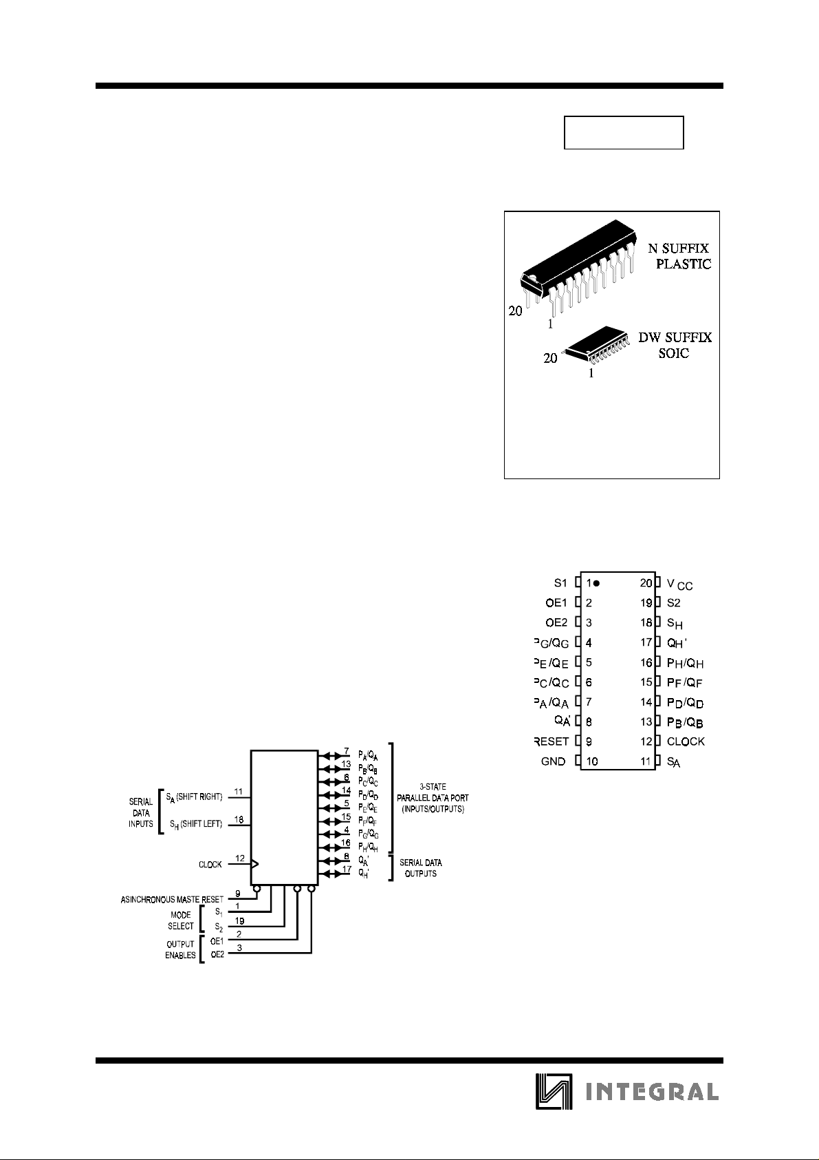
The IN74AC299 is identical in pinout to the LS/ALS299,
HC/HCT299. The device inputs are compatible with standard CMOS
outputs; with pullup resistors, they are compatible with LS/ALS
outputs.
The IN74AC299 features a multiplexed parallel input/output data
port to achieve full 8-bit handling in a 20 pin package. Due to the large
output drive capability and the 3-state feature, this device is ideally
suited for interface with bus lines in a bus-oriented system.
Two Mode-Select inputs and two Output Enable inputs are used to
choose the mode of operation as listed in the Function Table.
Synchronous parallel loading is accomplished by taking both ModeSelect lines, S
impedance state, which permits data applied to the data port to be
clocked into the register. Reading out of the register can be
accomplished when the outputs are enabled. The active-low
asynchronous Reset overrides all other inputs.
•
Outputs Directly Interface to CMOS, NMOS, and TTL
•
Operating Voltage Range: 2.0 to 6.0 V
•
Low Input Current: 1.0 µA; 0.1 µA @ 25°C
•
High Noise Immunity Characteristic of CMOS Devices
•
Outputs Source/Sink 24 mA
and S2, high. This places the outputs in the high-
1
IN74AC299
ORDERING INFORMATION
IN74AC299N Plastic
IN74AC299DW SOIC
TA = -40° to 85° C for all
packages
PIN ASSIGNMENT
LOGIC DIAGRAM
PIN 20=V
PIN 10 = GND
CC
386
IN74AC299
MAXIMUM RATINGS
*
Symbol Parameter Value Unit
V
CC
V
V
OUT
I
IN
I
OUT
I
CC
P
DC Supply Voltage (Referenced to GND) -0.5 to +7.0 V
DC Input Voltage (Referenced to GND) -0.5 to VCC +0.5 V
IN
DC Output Voltage (Referenced to GND) -0.5 to VCC +0.5 V
DC Input Current, per Pin
DC Output Sink/Source Current, per Pin
DC Supply Current, VCC and GND Pins
Power Dissipation in Still Air, Plastic DIP+
D
SOIC Package+
±
20
±
50
±
50
750
500
Tstg Storage Temperature -65 to +150
T
Lead Temperature, 1 mm from Case for 10 Seconds
L
260
(Plastic DIP or SOIC Package)
*
Maximum Ratings are those values beyond which damage to the device may occur.
Functional operation should be restricted to the Recommended Operating Conditions.
+Derating - Plastic DIP: - 10 mW/°C from 65° to 125°C
SOIC Package: : - 7 mW/°C from 65° to 125°C
mA
mA
mA
mW
°
C
°
C
RECOMMENDED OPERATING CONDITIONS
Symbol Parameter Min Max Unit
V
CC
VIN, V
T
J
T
A
I
OH
I
OL
tr, t
f
*
V
from 30% to 70% V
IN
This device c ontains p rote ction ci rcuitr y to guard a gainst damage d ue to high st atic voltages or electr ic
fields. However, precautions must be taken to avoid applications of any voltage higher than maximum rated
voltages to this high-impedance circuit. For proper operation, V
GND≤(V
Unused inputs must always be tied to an appropriate logic voltage level (e.g., either GND or V
Unused outputs must be left open.
DC Supply Voltage (Referenced to GND) 2.0 6.0 V
DC Input Voltage, Output Voltage (Referenced to GND) 0 V
OUT
Junction Temperature (PDIP) 140
Operating Temperature, All Package Types -40 +85
Output Current - High -24 mA
Output Current - Low 24 mA
Input Rise and Fall Time
(except Schmitt Inputs)
IN
or V
OUT
)≤VCC.
CC
*
V
V
V
=3.0 V
CC
=4.5 V
CC
=5.5 V
CC
and V
IN
0
0
0
should be constrained to the range
OUT
CC
150
40
25
V
°
C
°
C
ns/V
CC
).
387
IN74AC299
DC ELECTRICAL CHARACTERISTICS
(Voltages Referenced to GND)
Symbol Parameter Test Conditions V
V
Minimum High-Level
IH
V
=0.1 V or VCC-0.1 V 3 .0
OUT
Input Voltage
V
Maximum Low -
IL
V
=0.1 V or VCC-0.1 V 3 .0
OUT
Level Input Voltage
V
OH
Minimum High-Level
I
OUT
≤ -50 µA
Output Voltage
*
VIN=VIH or V
IL
IOH=-12 mA
I
=-24 mA
OH
I
=-24 mA
OH
V
OL
Maximum Low-Level
I
OUT
≤ 50 µA
Output Voltage
*
VIN= VIH or V
IL
IOL=12 mA
I
=24 mA
OL
I
=24 mA
OL
I
IN
Maximum Input
VIN=VCC or GND 5.5
Leakage Current
I
I
OZ
OLD
Maximum ThreeState Leakage
Current
+Minimum Dynamic
V
(OE)= VIH or V
IN
V
V
V
or GND
IN =VCC
OUT =VCC
OLD
or GND
=1.65 V Max 5.5 75 mA
IL
Output Current
I
OHD
+Minimum Dynamic
V
=3.85 V Min 5.5 -75 mA
OHD
Output Current
I
CC
Maximum Quiescent
VIN=VCC or GND 5.5 8.0 80
Supply Current
(per Package)
*
All outputs loaded; thresholds on input associated with output under test.
+Maximum test duration 2.0 ms, one output loaded at a time.
Note: I
IN
and I
@ 3.0 V are guaranteed to be less than or equal to the respective limit @ 5.5 V V
CC
V
4.5
5.5
4.5
5.5
3.0
4.5
5.5
3.0
4.5
5.5
3.0
4.5
5.5
3.0
4.5
5.5
5.5
CC
Guaranteed Limits
25 °C-40
2.1
3.15
3.85
0.9
1.35
1.65
2.9
4.4
5.4
2.56
3.86
4.86
0.1
0.1
0.1
0.36
0.36
0.36
±
0.1
±
0.6
°
C to
85°C
2.1
3.15
3.85
0.9
1.35
1.65
2.9
4.4
5.4
2.46
3.76
4.76
0.1
0.1
0.1
0.44
0.44
0.44
±
1.0
±
6.0
CC
Unit
V
V
V
V
µ
A
µ
A
µ
A
388
 Loading...