

INTEGRAL ILA7053N Datasheet
TECHNICAL DATA
1
INTEGRAL
2 x 1 W portable/mains-fed stereo
power amplifier
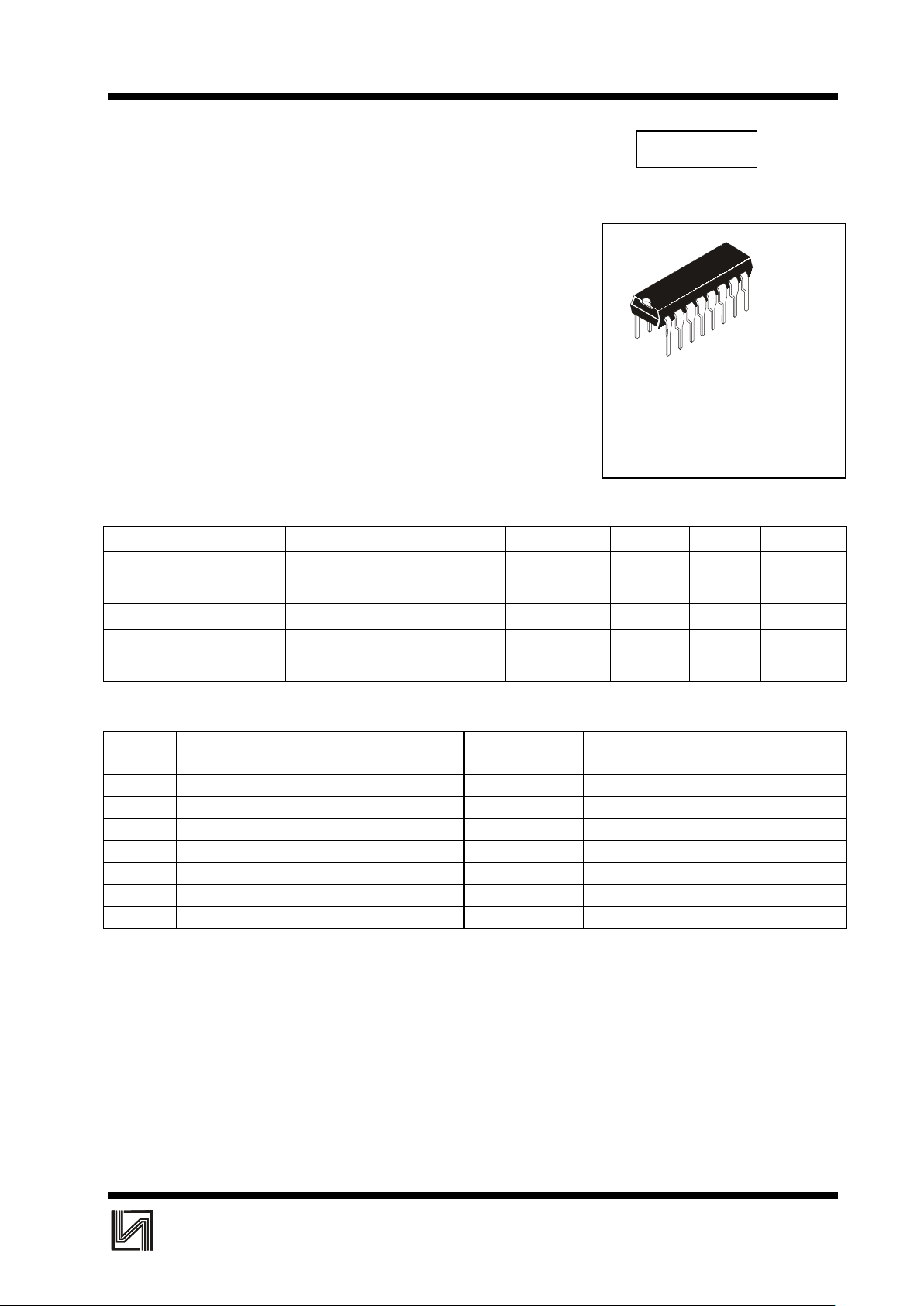
The ILA7053N is an integrated class-B stereo power amplifier in a 16-lead
dual-in-line (DIL) plastic package. The device, consisting of two BTL
amplifiers, is primarily developed for portable audio applications but may
also be used in mains-fed applications.
• No external components
• No switch-ON/OFF clicks
• Good overall stability
• Low power consumption
• Short-circuit-proof
QUICK REFERENCE DATA
PARAMETER CONDITIONS SYMBOL MIN. MAX. UNIT
Supply voltage range V
P
318V
Total quiescent current
R
L
= ∞
I
tot
-16mA
Output power
R
L
= 8 Ω, V
P
= 6 V, THD = 10%
P
O
-1W
Internal voltage gain
R
L
= 8 Ω, V
P
= 6 V
Gv 38 40 dB
Total harmonic distortion
P
O
= 0.1 W, R
L
= 8 Ω, V
P
= 6 V
THD - 1.0 %
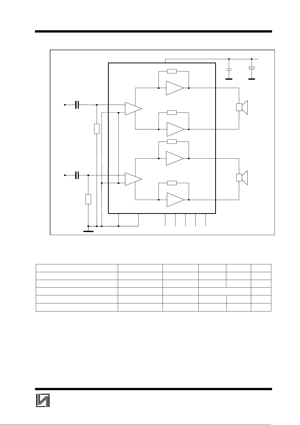
PINNING
Pin № Symbol Description Pin № Symbol Description
01 SGND1 signal ground 1 09 OUT2A output 2 (positive)
02 IN1 input 1 10 GND2 power ground 2
03 n.c. not connected 11 n.c. not connected
04 n.c. not connected 12 OUT2B output 2 (negative)
05 V
P
supply voltage 13 OUT1B output 1 (negative)
06 IN2 input 2 14 GND1 power ground 1
07 SGND2 signal ground 2 15 n.c. not connected
08 n.c. not connected 16 OUT1A output 1 (positive)
Note
The information contained within the parentheses refer to the polarity of the loudspeaker terminal to which the
output must be connected.
FUNCTIONAL DESCRIPTION
The ILA7053N is a stereo output amplifier, with an internal gain of 39 dB, which is primarily for use in portable
audio applications but may also be used in mains-fed applications. The current trends in portable audio application
design is to reduce the number of batteries which results in a reduction of output power when using conventional
output stages.
The ILA7053N overcomes this problem by using the Bridge-Tied-Load (BTL) principle and is capable of delivering
1.2 W into an 8 Ω load (V P = 6 V). The load can be short-circuited under all input conditions.
ILA7053N
N SUFFIX
1
16
ORDERING INFORMATION
ILA7053N Plastic DIP
T
A
= -25 ° to +70° C
ILA7053N
2
INTEGRAL
Fig.1 Block diagram, test and application circuit diagram
RATINGS
Limiting values in accordance with the Absolute Maximum System
PARAMETER CONDITIONS SYMBOL MIN. MAX. UNIT
Supply voltage V
P
-18V
Non-repetitive peak output current I
OSM
-1.5A
Total power dissipation P
tot
see Fig.2
Crystal temperature Tc - +150
°C
Storage temperature range Tstg -60 +150
°C
THERMAL RESISTANCE
From junction to ambient R
th j-a
60 K/W
Power dissipation
Assuming: VP = 6 V and R
L
= 8 Ω:
The maximum sinewave dissipation is 1.8 W, therefore T
amb(max.)
= 150 - (60 x 1.8) = 42°C.
05
02
01
16
13
+Vp
Rs=5,1
k
ΩΩΩΩ
RL
1
0,1
µµµµ
F
220,0
µµµµ
F
+
-
+
_
Cin=(0, 47 -1 0,0)
µµµµ
F
S
G
N
D
1
06
07
10
12
09
Rs=5,1
k
ΩΩΩΩ
RL
2
GND-2
S
G
N
D
2
14
GND-1
ILA7053N
11 150803 04
Vi2
Vi1
Cin=(0, 47 -1 0,0)
µµµµ
F
-
+
 Loading...