

INTEGRAL IL358N, IL358D Datasheet
TECHNICAL DATA
Low Power Dual Operational Amplifier
The IL358 contains two independent high gain operational
amplifiers with internal frequency compensation. The two op-amps
operate over a wide voltage range from a single power supply. Also
use a split power supply. The device has low power supply current
drain, regardless of the power supply voltage. The low power drain
also makes the IL358 a good choice for battery operation.
When your project calls for a traditional op-amp function, now you
can streamline your design with a simple single power supply. Use
ordinary +5V
computer application, without requiring an extra 15V power supply
just to have the interface electronics you need.
The IL358 is a versatile, rugged workhorse with a thousand-andone uses, from amplifying signals from a variety of transducers to dc
gain blocks, or any op-amp function. The attached pages offer some
recipes that will have your project cooking in no time.
• Internally frequency compensated for unity gain
• Large DC voltage gain: 100dB
• Wide power supply range:
• Input common-mode voltage range includes ground
• Large output voltage swing: 0V DC to V
• Power drain suitable for battery operation
• Low input offset voltage and offset current
• Differential input voltage range equal to the power supply voltage
DC
common to practically any digital system or personal
3V ~ 32V (or ±1.5V ~ ±16V)
-1.5V DC
CC
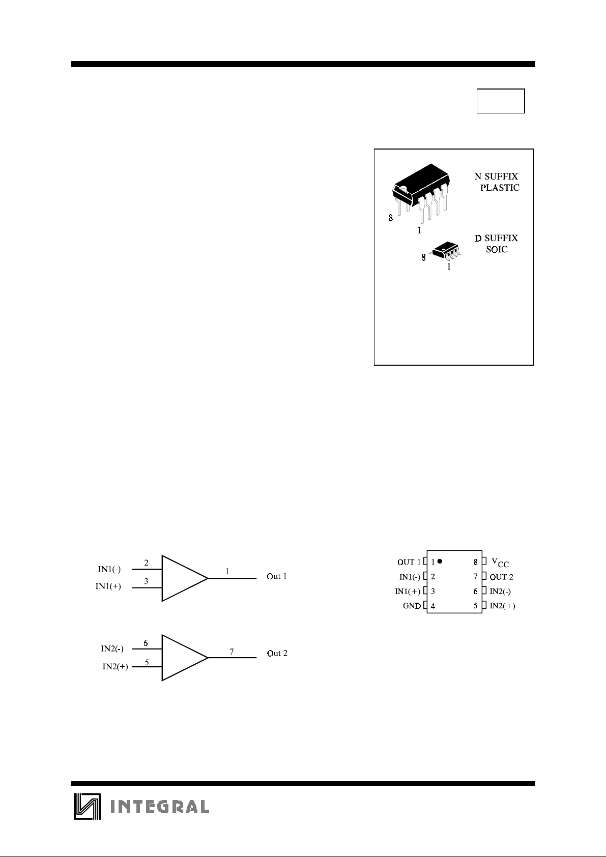
IL358
ORDERING INFORMATION
IL358N Plastic
IL358D SOIC
TA = 0° to 70° C
for all packages
.
LOGIC DIAGRAM
PIN 4 = GND
PIN 8=V
CC
PIN ASSIGNMENT
1
IL358
MAXIMUM RATINGS
*
Symbol Parameter Value Unit
V
CC
V
IDR
V
ICR
I
SC
T
Power Supply Voltages
Single Supply
Split Supplies
Input Differential Voltage Range (1)
32
±16
±32
Input Common Mode V oltage Range -0.3 to 32 V
Output Short Circuit Duration Continuous
Junction Temperature
J
Plastic Packages 150
Tstg Storage Temperature
Plastic Packages -55 to +125
I
IN
T
*
Maximum Ratings are those values beyond which damage to the device may occur.
Input Current, per pin (2) 50 mA
Lead Temperature, 1mm from Case for 10 Seconds 260
L
Functional operation should be restricted to the Recommended Operating Conditions.
+Derating - Plastic DIP: - 10 mW/°C from 65° to 125°C
SOIC Package: : - 7 mW/°C from 65° to 125°C
Notes:
1. Split Power Supplies.
2. V
<-0.3V. This input current will only exist when voltage at any of the input leads is driven negative.
IN
V
V
°C
°C
°C
RECOMMENDED OPERATING CONDITIONS
Symbol Parameter Min Max Unit
V
CC
T
A
DC Supply Voltage
±2.5 or
5.0
±15 or
30
Operating Temperature, All Package Types 0 +70
This device c ontains p rote ction ci rcuitr y to guard a gainst damage d ue to high st atic voltages or electr ic
fields. However, precautions must be taken to avoid applications of any voltage higher than maximum rated
voltages to this high-impedance circuit. For proper operation, V
GND≤(V
IN
or V
OUT
)≤VCC.
and V
IN
should be constrained to the range
OUT
Unused inputs must always be tied to an appropriate logic voltage level (e.g., either GND or V
Unused outputs must be left open.
V
°C
CC
).
2
 Loading...