

INTEGRAL IL34118N, IL34118DW Datasheet
Voice Switched Speakerphone Circuit
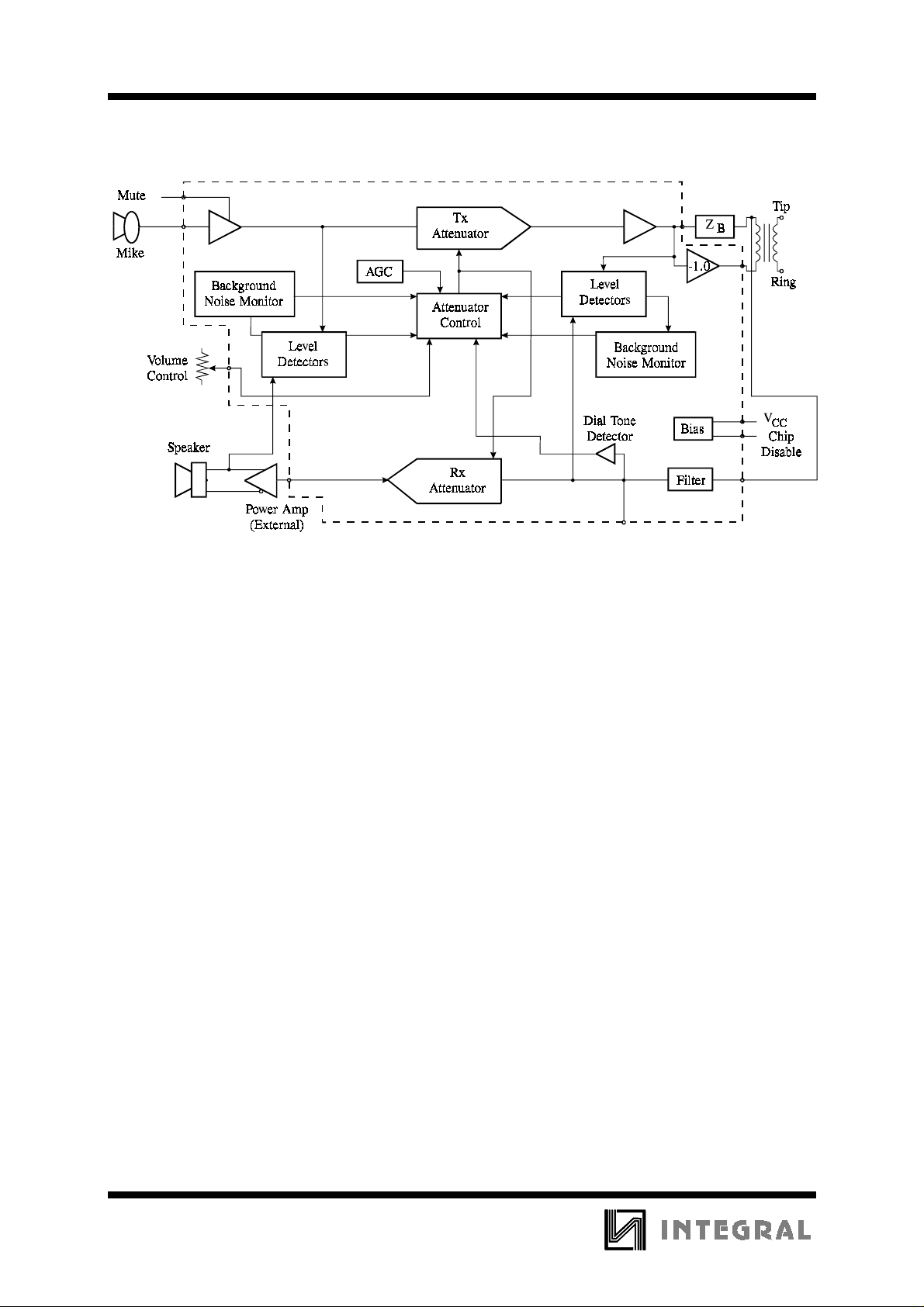
The IL34118 Voice Switched Speakerphone Circuit incorporates
the necessary amplifiers, attenuators, level detectors, and control
algorithm to form the heart of a high quality hands-free speakerphone
system. Included are a microphone amplifier with adjustable gain and
MUTE control, Transmit and Receive attenuators which operate in a
complementary manner, level detectors at both input and output of
both attenuat ors, and backgro und noise monito rs for b oth the t ransmit
and receive channels. A Dial Tone Detector prevents the dial tone
from being attenuated by the Receive background noise monitor
circuit. Also included are two line driver amplifiers which can be used
to form a hybrid network in conjunction with an external coupling
transformer. A high pass filter can be used to filter out 60 Hz noise in
the reseive channel, or for other filtering functions. A Chip Disable
pin permits powering down the entire circuit to conserve power on
long loops where loop current is at a minimum.
The IL34118 may be operated from a power supply, or it can be
powered from the telephone line, requiring typically 5.0 mA. The
IL34118 can be interfaced directly to Tip and Ring (through a
coupling transformer) for stand-alone operation, or it can be used in
conjunction with a handset speech network and or other features of a
featurephone.
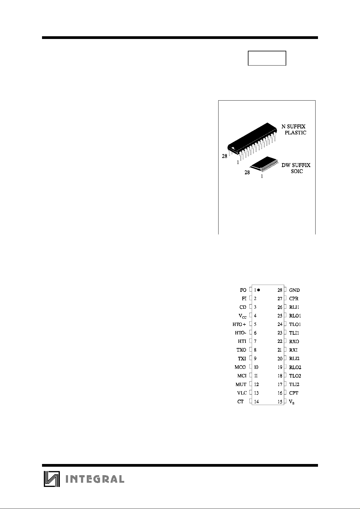
TECHNICAL DATA
IL34118
ORDERING INFORMATION
IL34118N Plastic
IL34118DW SOIC
TA = -25° to 70° C for all packages
•
Improved Attenuator Gain Range: 52 dB Between Transmit and
Receive
•
Low Voltage Operation for Line-Powered Applications (3.0-
6.5 V)
•
4 Point Signal Sensing for Improved Sensitivity
•
Background Noise Monitors for Both Transmit and Receive
Paths
•
Microphone Amplifier Gain Set by External Resistors - Mute
Function Include d
•
Chip Disable for Active Standby Operation
•
On Board Filter Pinned-Out for User Deined Function
•
Dial Tone Detector to Inhibit Receive Idle Mode During Dial
Tone Presence
PIN ASSIGNMENT
1
IL34118
SIMPLIFIED BLOCK DIAGRAM
FUNCTIONAL DESCRIPTION
INTRODUCTION
The fundamental difference between the operation
of a speakerphone and a handset is that of half-duplex
versus full-duplex. The handset is full duplex since
conversation can occur in both directions (transmit
and receive) simultaneousiy. A speakerphone has
higher gain levels in both paths, and attempting to
converse full duplex results in oscillatory problems
due to the loop that exists within the system. The loop
is formed by the receive and transmit paths, the
hybrid, and the acoustic coupling (speaker to
microphone). The only practical and economical
solution used to data is to design the speakerphone to
function in a half duplex mode - i.e., only one person
speaks at a time, while the other listens. To achieve
this requires a circuit which can detect who is talking,
switch on the appropriate path (transmit or receive),
and switch off (attenuate) the other path. In this way,
the loop gain is maintained less than unity. When the
talkers exchange function, the circuit must quickly
detect this, and switch the circuit appropriately.By
providing speech level detectors, the circuit operates
in a “hand-free” mode, eliminating the need for a
“push-to-talk” switch.
The handset, by the way, has the same loop as the
speakerphone. But since the gains are considerably
lower, and since the acoustic coupling from the
earpiece to the mouthpiece is almost non-existent (the
receiver is normally held against a person’s ear),
oscillations don’t occur.
The IL34118 provides the necessary level
detectors, attenuators, and switching control for a
properly operating speakerphone. The detection
sensitivity and timing are externally controllable.
Additionally, the IL34118 provides background noise
monitors which make the circuit insensitive to room
and line noise, hybrid amplifiers for interfacing to
Tip and Ring, the microphone amplifier, and other
associated functions.
ATTENUATORS
The transmit and receive attenuators are
complementary in function, i.e., when one is at
maximum gain (+6.0 dB), the other is at maximum
attenuation (-46 dB), and vice versa. They are never
both fully on or both fully off. The sum of their gains
remains constant (within a nominal error band of
±
0.1 dB) at a typical value of -40 dB. Their purpose
is to control the transmit and receive paths to provide
the half-duplex operation required in a speakerphone.
The attenuators are non-inverting, and have a -
3.0 dB (from max gain) freque ncy of ≈100 KHz. The
input impedance of each attenuator (TXI and RXI) is
nominally 10 kΩ (see Figure 1), and the input signal
should be limited to 350 mVrms (990 mVp-p) to
prevent distortion. That maximum
2
IL34118
recommended input signal is independent of the
volume control setting. The diode clamp on the
inputs limits the input swing, and therefore the
maximum negative output swing. This is the reason
for V
RXOL
and V
specification being defined as
TXOL
they are in the Electrical Characteristics. The output
impedance is <10 Ω until the output current limit
(typically 2.5 mA) is reached.
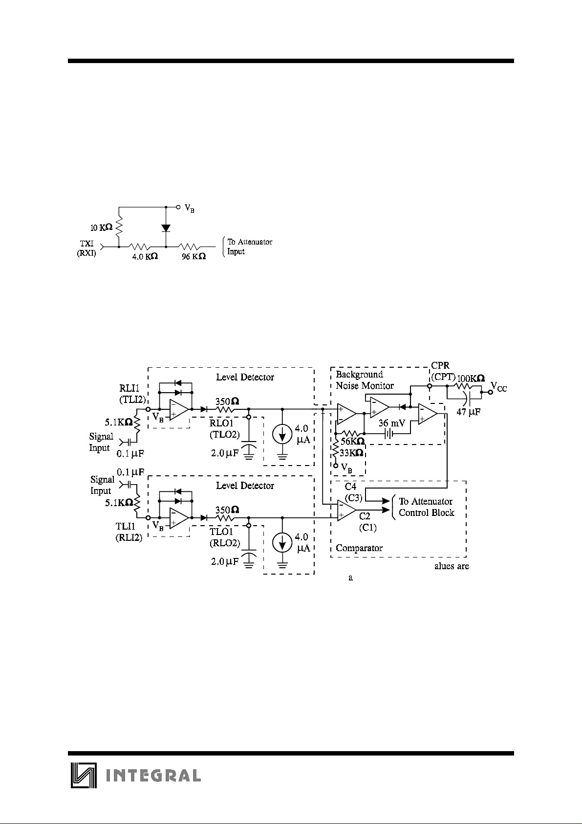
Figure 1. Attenuator Input Stag e
The attenuators are controlled by the single output
of the Control Block, which is measurable at the C
pin (Pin 14). When the C
with respect to V
, the circuit is in the receive mode
B
(receive attenuator is at +6.0 dB). When the C
pin is at +240 millivolts
T
pin is
T
Figure 2. Level Detectors
at -240 millivolts with respect to V
, the circuit is in
B
the transmit mode (transmit attenuator is at +6.0 dB).
The circuit is in an idle mode when the C
equal to V
, causing the attenuators’ gains to be
B
halfway between their fully on and fully off positions
(-20 dB each). Monitoring the C
respect to V
) is the most direct method of
B
T
monitoring the circuit’s mode.
The inputs to the Control Block are seven: 2 from
the comparators operated by the level detectors, 2
from the background noise monitors, the volume
control, the dial-tone detector, and the AGC circuit.
These seven inputs are described below.
LEVEL DETECTORS
There are four level detectors - two on the receive
side and two on the transmit side. Refer to Figure 2 -
T
the terms in parentheses form one system, and the
other terms form the second system
voltage is
T
voltage (with
Each level detector is a high gain amplifier with
back-to-back diodes in the feedback path, resulting in
non-linear gain, which permits operation over a wide
dynamic range of speech levels. The sensitivity of
each level detector is determined by the external
resistor and capacitor at each input (TLI1, TLI2,
RLI1, and RLI2). Each output charges an external
capacitor through a diode and limiting resistor, thus
providing a dc representation of the input ac signal
level. The o utputs have a guick rise t ime (de termined
by the capacitor and an internal 350 Ω resistor), and a
slow decay time set by an internal current source and
the capacitor. The capacitors on the four outputs
should have the same value (±10%) to prevent timing
problems.
Referring to Figure 8, on the receive side, one
level detector (RLI1) is at the receive input receiving
the same signal as at Tip and Ring, and
3
IL34118
the other (RLI2) is at the output of the speaker
amplifier. On the transmit side, one level detector
(TLI2) is at the output of the microphone amplifier,
while the other (TLI1) is at the hybrid output.
Outputs RLO1 and TLO1 feed a comparator, the
output of which goes to the Attenuator Control Block.
Likewise, outputs RLO2 and TLO2 feed a second
comparator which also goes to the Attenuator Control
Block. The truth table for the effects of the level
detectors on the Control Block is given in the section
describing the Control Block.
BACKGROUND NOISE MONITORS
The purpose of the background noise monitors is
to distinguish speech (which consists of bursts) from
background no ise (a relativel y constant signal level).
There are two background noise monitors - one for
the receive path and one for the transmit path.
Refering to Figure 2, the receive background noise
monitor is operated on by the RLI1-RLO1 level
detector, while the transmit background noise
monitor is operated on by the TLI2-TLO2 level
detector. They monitor the background noise by
storing a dc voltage representative of the respective
noise levels in capacitors at CPR and CPT. The
voltages at these pins have slow rise times
(determined by the external RC), but fast decay times.
If the signal at RLI1 (or TLI2) changes slowly, the
voltage at CPR (or CPT) will remain more positive
than the voltage at the non-inverting input of the
monitor’s output comparator. When speech is
present, the voltage on the noninverting input of the
comparator will rise quicker than the voltage at the
inverting input (due to the burst characteristic of
speech), causing its output to change. This output is
sensed by the Attenuator Control Block.
The 36 mV offset at the comparator’s input keeps
the comparator from changing state unless the speech
level exceeds the background noise by ≈4.0 dB. The
time constant of the external RC (≈4.7 seconds)
determines the response time to background noise
variations
VOLUME CONTROL
The volume control input at VLC (Pin 13) is
sensed as a voltage with respect to V
control affects the attenuators only in the receive
mode. It has no effect in the idle or transmit modes.
When in the receive mode, the gain of the receive
attenuator will be +6.0 dB, and the gain of the
transmit attenuator will be -46 dB only when VLC is
equal to V
. As VLC is reduced below VB,
B
. The volume
B
the gain of the receive attenuator is reduced, and the
gain of the transmit attenuator is increased such that
their sum remains constant. Changing the voltage at
VLC changes the voltage at C
(see the Attenuator
T
Control Block section), which in turn controls the
attenuators.
The volume control setting does not affect the
maximum attenuator input signal at which notice able
distortion occurs.
The bias current at VLC is typically 60 nA out of
the pin, and does not vary significantly with the VLC
voltage or with V
CC
.
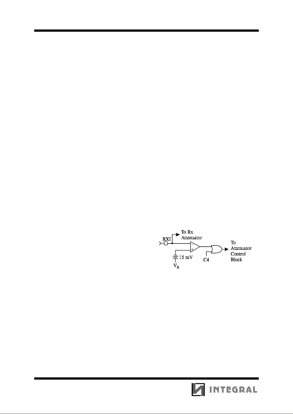
DIAL TONE DETECTOR
The dial tone detector is a comparator with one
side connected to the receive input (RXI) and the
other input connected to V
with a 15 mV offset (see
B
Figure 3). If the circuit is in the receive mode, and the
incoming signal is greater than 15 mV (10 mVrms),
the comparator’s output will change, disabling the
receive idle mode. Tthe receive attenuator will then
be at a setting determined solely by the volume
control.
The purpose of this circuit is to prevent the dial
tone (which would be considered as continuous
noise) from fading away as the circuit would have the
tendency to swich to the idle mode. By disabling the
receive idle mode, the dial tone remains at the
normally expected full level.
Figure 3. Dial Tone Detector
AGS
The AGS circuit affects the circuit only in the
receive mode, and only when the supply voltage
(V
) is less than 3.5 volts. As VCC falls below
CC
3.5 volts, the gain of the receive attenuator is
reduced. The transmit path attenuation changes such
that the sum of the transmit and receive gains remains
constant.
The purpose of this feature is to reduce the power
(and current) used by the speaker when a linepowered speakerphone is connected to a long line,
where the available power is limited. By reducing the
speaker power, the voltage sag at V
preventing possible erratic operation.
is controlled,
CC
4
 Loading...