

INTEGRAL IL34063AP1, IL34063AD Datasheet
34063A
DC-TO-DC CONVERTER CONTROL CIRCUITS
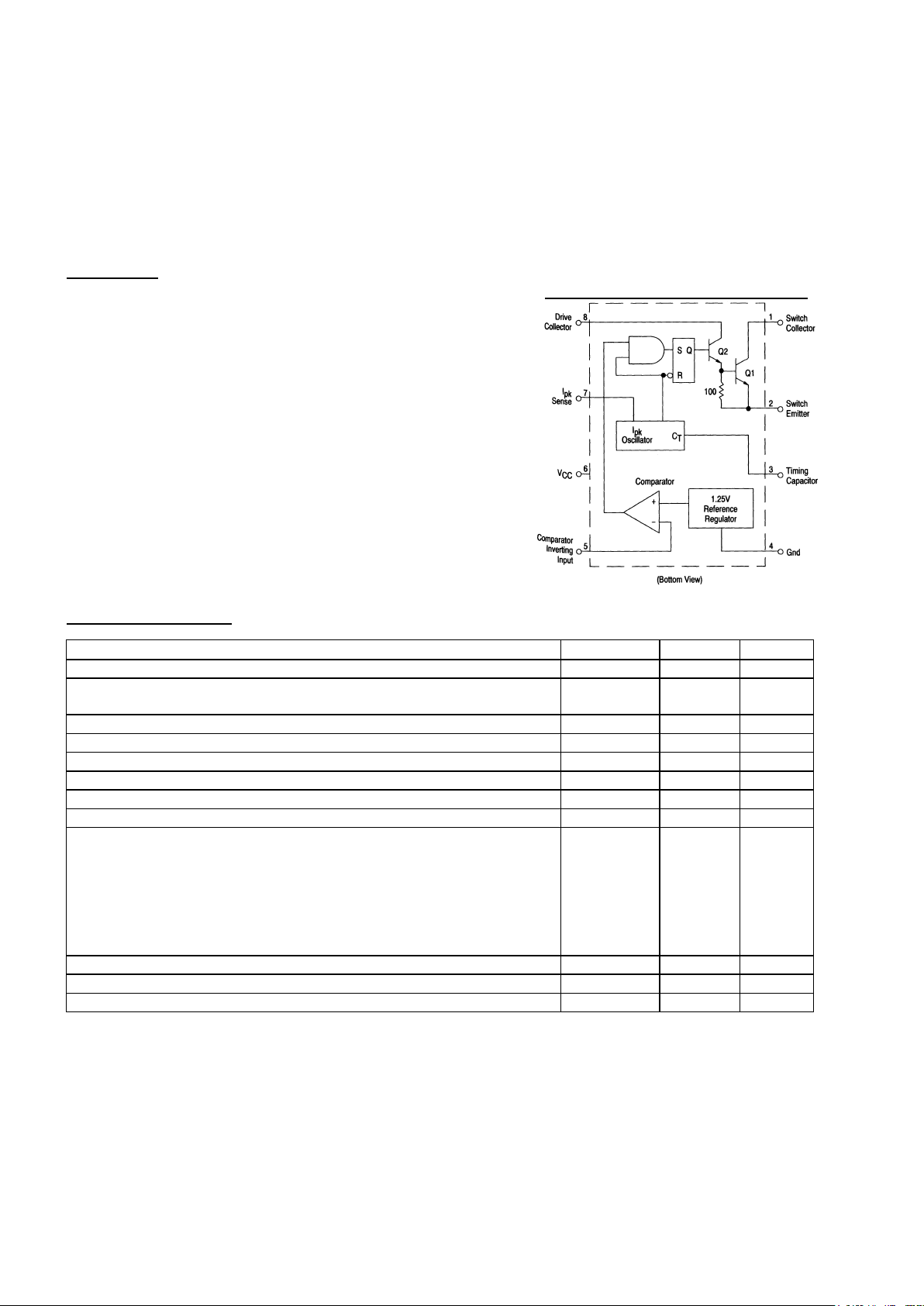
The 34063A is a monolithic control circuit containing the primary functions required for DC-to-DC converters.
These devices consist of an internal temperature compensated reference, comparator, controlled duty cycle
oscillator with an active current limit circuit, driver and high current output switch. This series was specifically
designed to be incorporated in Step-Down and Step-Up and Voltage-Inverting applications with a minimum number
of external components.
FEATURES
FUNCTIONAL BLOCK DIAGRAM
• Operation from 3.0 V to 40 V Input
• Low Standby Current
• Current Limiting
• Output Switch Current to 1.5 A
• Output Voltage Adjustable
• Frequency Operation to 100 kHz
• Precision 2% Reference
MAXIMUM RATINGS
Rating Symbol Value Unit
Power Supply Voltage VCC 40 Vdc
Comparator Input Voltage Range VIR -0.3 to
+40
Vdc
Switch Collector Voltage V
C(switch)
40 Vdc
Switch Emitter Voltage (Vpin 1 = 40 V) V
E(switch)
40 Vdc
Switch Collector to Emitter Voltage V
CE(switch)
40 Vdc
Driver Collector Voltage I
C(driver)
40 Vdc
Driver Collector Current (Note 1) I
C(driver)
100 mA
Switch Current ISW 1.5 A
Power Dissipation and Thermal Characteristics
Ceramic Package, U Suffix T
A
= +25°C
Thermal Resistance
Plastic Package, P Suffix T
A
= +25°C
Thermal Resistance
SOIC Package, D Suffix
TA = +25°C
Thermal Resistance
P
D
R
θJA
P
D
R
θJA
P
D
R
θJA
1.25
100
1.25
100
625
160
W
°C/W
W
°C/W
mW
°C/W
Operating Junction Temperature TJ +150 °C
Operating Ambient Temperature Range TA 0 to +70 °C
Storage Temperature Range Tstg -65to+150 °C
ORDERING INFORMATION
Device Temperature
Range
Package
34063AD 0° to +70°C SO-8
34063AP1 Plastic DIP
ELECTRICAL CHARACTERICISTICS
(V
CC
= 5.0 V, T
A
= 0 to +70oC unless otherwise specified.)
Characteristics Symbol Min Typ Max Unit
OSCILLATOR
Frequency (V
Pin 5
= 0 V, C
T
= 1.0 nF, TA = 25°C) f
osc
24 33 42 kHz
Charge Current (V
CC
= 5.0 V to 40 V, TA = 25°C) I
chg
24 33 42
µA
Discharge Current (V
CC
= 5.0 V to 40 V, TA = 25°C) I
dischg
140 200 260
µA
Discharge to Charge Current Ratio (Pin7 to Vcc, TA=25°C)
I
dischg/Ichg
5.2 6.2 7.5 —
Current Limit Sense Voltage (Ichg = Idischg, T
A
= 25°C)
V
lpk
(sense) 250 300 350 mV
OUTPUT SWITCH (Note 3)
Saturation Voltage, Darlington Connection (ISW = 1.0 A,
Pins 1, 8 connected)
V
CE
(sat) — 1.0 1.3 V
Saturation Voltage (ISW = 1.0 A, R
Pin 8
= 82 Ω to VCC.
Forced β = 20)
V
CE
(sat) — 0.45 0.7 V
DC Current Gain (ISW = 1.0 A, V
CE
=
5.0 V, T
A
= 25°C) h
FE
50 120 — —
Collector Off-State Current (V
CE
= 40V) I
C
(off) — 0.01 100
µA
COMPARATOR
Threshold Voltage (T
A
= 25°C)
(T
A
= T
LOW
to T
HIGH
)
Vth 1.225
1.21
1.25
—
1.275
1.29
V
Threshold Voltage (T
A
= 25°C) **
Vth 1.2375
1.25
1.2625 V
Threshold Voltage Line Regulation (V
CC
= 3.0 V to 40 V)
V
REG line
1.4 5.0 mV
Input Bias Current (Vin=0V)
IIB — -40 -400 nA
TOTAL DEVICE
Supply Current (V
CC
= 5 0 V to 40 V, CT = 1 0 nF, V
pin7
=
V
CC
. V
Pin5
> Vth, Pin 2 = Gnd, Remaining pins open)
ICC 2.5 4.0 mA
NOTES:
1. Maximum package power dissipation limits must be observed.
2. Low duty cycle pulse techniques are used during test to maintain Junction temperature as close to ambient
temperature as possible
3. If the output switch is driven into hard saturation (non Darlington configuration) at low switch currents (< 300 mA) and
high driver currents (>30 mA), it may take up to 2.0 µs to come out of saturation This condition will shorten the off' time
at frequencies > 30 kHz, and is magnified at high temperatures This condition does not occur with a Darlington configuration,
since the output switch cannot saturate If a non Darlington configuration is used, the following output drive condition is
recommended
Forced β of output switch = I
C
, output/(Ic, driver -7.0 mA*) > 10
*The 100 Ω. resistor in the emitter of the driver device requires about 7.0 mA before the output switch conducts
**Possible version for shipment
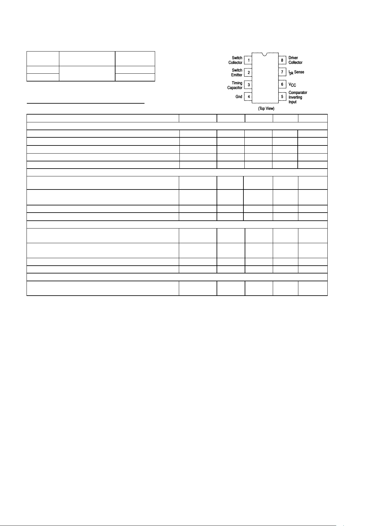
Pin connection
 Loading...