

Page 1
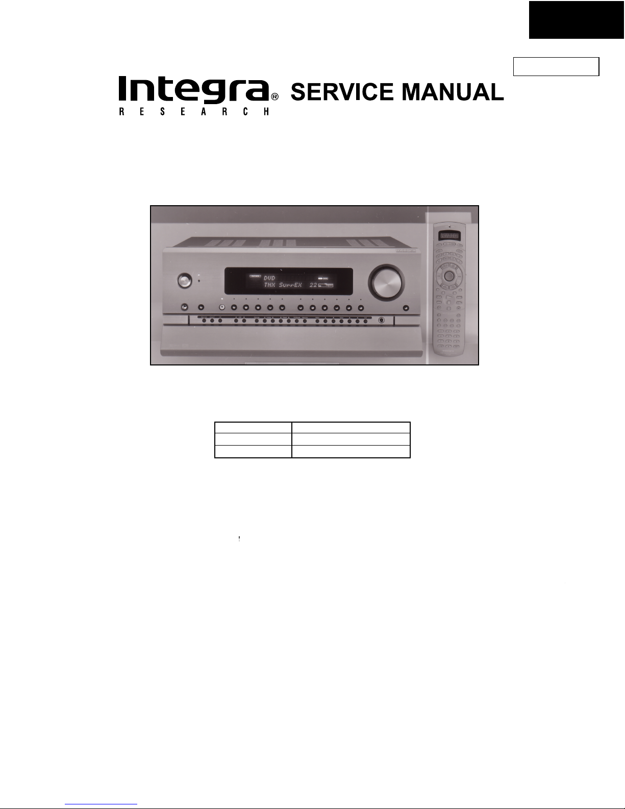
AV Controller
MODEL RDC-7
SAFETY-RELATED COMPONENT WARNING!!
COMPONENTS IDENTIFIED BY MARK ON THE
SCHEMATIC DIAGRAM AND IN THE PARTS LIST
ARE CRITICAL FOR RISK OF FIRE AND ELECTRIC SHOCK. REPLACE THESE COMPONENTS
WITH ONKYO PARTS WHOSE PARTS NUMBERS
APPEAR AS SHOWN IN THIS MANUAL.
MAKE LEAKAGE-CURRENT OR RESISTANCE
MEASUREMENTS TO DETERMINE THAT EXPOSED PARTS ARE ACCEPTABLY INSULATED FORM
THE SUPPLY CIRCUIT BEFORE RETURNING THE
APPLIANCE TO THE CUSTOMER.
No.3653
RDC-7
Sep,2000
Silver model
UDD, UDT
UPP,UPT
UGT
120V AC, 60Hz
220 -230V AC, 50/60Hz
230V AC, 50Hz
SPECIFICATIONS--------------------------------------------------------
SERVICE PROCEDURE
-------------------------------------------------
FRONT PANEL FACILITIES
--------------------------------------------
REMOTE CONTROLLER
-----------------------------------------------
REAR PANEL FACILITIES
------------------------------------------------
EXAMPLE OF HOW TO CONNECT YOUR EQUIPMENT
-------
CONNECTING POWER AMPLIFIERS
---------------------------------
DISASSEMBLING PROCEDURES
---------------------------------------
ASSEMBLING PROCEDURES--------------------------------------------
IC BLOCK DIAGRAMS AND DESCRIPTIONS----------------------
WIRING VIEW--------------------------------------------------------------
CHASSIS EXPLODED VIEW--------------------------------------------
CHASSIS EXPLODED VIEW PARTS LIST-----------------------------
MAIN MICROPROCESSOR CONNECTION DIAGRAM-----------
MAIN MICROPROCESSOR TERMINAL DESCRIPTION---------
SUB MICROPROCESSOR CONNECTION DIAGRAM-------------
SUB MICROPROCESSOR TERMINAL DESCRIPTION------------
PC BOARD CONNECTION VIEW---------------------------------------
BLOCK DIAGRAM--------------------------------------------------------
PRINTED CIRCUIT BOARD PARTS LIST-------------------SCHEMATIC DIAGRAM /
PRINTED CIRCUIT BOARD VIEW-----------------
CONFIRMATION
-----------------------------------------------------------
FL TUBE VIEW--------------------------------------------------------------
P A CKING VIEW --------------------------------------------------------------
2
3
4
5
6
8
10
11
12
13~30
31
33
35
37
39
41
43
45
47
49
50~94
95
96
97
TABLE OF CONTENTS
Page 2

RDC-7
2
GENERAL
Power Supply AC 120 V, 60 Hz
AC 230 V, 50 Hz
AC 220 V, 50/60 Hz
Power Consumption 75 W
Dimensions (W H D) 450 196 440 mm
17-11/16" 7-11/16" 17-5/16"
Weight 16.2 kg, 35.7 lbs.
REMOTE CONTROLLER
Transmitter Infrared
Signal range Approx. 5 meters, 16 ft.
Power supply Two “AA” batteries (1.5 V 2)
Specifications and features are subject to change without
notice.
Power supply and voltage vary depending on the area in
which the unit is purchased.
CONTROLLER SECTION
Input Sensitivity and Impedance
PHONO 2.5 mV, 50 kohms
LINE (CD, TAPE 1-2, DVD,
VIDEO 1-5) 200 mV, 50 kohms
MULTICHANNEL INPUT
(FRONT L/C/R, SURROUND
L/R, SURROUND BACK L/R) 200 mV, 50 kohms
(SUBWOOFER) 36 mV, 50 kohms
COAXIAL 1-5 (DIGITAL) 0.5 Vp-p, 75 ohms
DVD, VIDEO1-5 1 Vp-p, 75 ohms
1 Vp-p, 75 ohms (Y)
0.28 Vp-p, 75 ohms (C)
COMPONENT VIDEO 1-3 1 Vp-p, 75 ohms (Y)
0.5 Vp-p, 75 ohms (P
B , PR )
Output Level and Impedance
Rec out (TAPE 1-2, VIDEO 1-2)
200 mV, 2.2 kohms
Pre out(RCA)
1 V, 470 ohms
Pre out(XLR)
1 V, 470 ohms
ZONE 2 OUT
100mV, 470 ohms
VIDEO (VIDEO 1-2, MONITOR
OUT, ZONE 2 OUT)
1 Vp-p, 75 ohms
1 Vp-p, 75 ohms (Y)
0.28 Vp-p, 75 ohms (C)
COMPONENT VIDEO OUT
1 Vp-p, 75 ohms (Y)
0.5 Vp-p, 75 ohms (P
B , PR)
Phono Overload
110 mV RMS at 1 kHz, 0.5% T.H.D.
Frequency Response
20 Hz to 30 kHz : 1dB
(CD in, Direct mode)
5 Hz to 100 kHz : +1dB,-3dB
(CD in, Direct mode)
RIAA Deviation:
20 to 20 kHz : 0.8 dB
Tone Control
Bass
10 dB at 100 Hz
Treble
10 dB at 10 kHz
Signal-to-Noise Ratio (Stereo)
PHONO
80 dB (IHF A, 5 mV input)
CD/TAPE
100 dB (IHF A, 0.5 V input)
TUNER SECTION
FM
Tuning Range
87.5 — 108.0 MHz (50 kHz steps)
Usable Sensitivity
Mono
11.2 dBf, 1.0 µV (75 ohms IHF)
0.9 µV (75 ohms DIN)
Stereo:
17.2 dBf, 2.0 µV (75 ohms IHF)
23 µV (75 ohms DIN)
50 dB Quieting Sensitivity
Mono
17.2 dBf, 2.0 µV (75 ohms)
Stereo
37.2 dBf, 20 µV (75 ohms)
Capture Ratio
2.0 dB
Image Rejection Ratio
USA & Canadian models
40 dB
European & Australian models
:
85 dB
IF Rejection Ratio
90 dB
Signal-to-Noise Ratio
Mono
76 dB
Stereo
70 dB
Alternate Channel Attenuation
55 dB
Selectivity
50 dB (DIN)
AM Suppression Ratio
50 dB
Total Harmonic Distortion
Mono
0.2 %
Stereo
0.3 %
Frequency Response
30 Hz — 15 kHz, 1.0 dB
Stereo Separation
45 dB at 1 kHz
30 dB at 100 Hz — 10 kHz
AM
Tuning Range
USA & Canadian models
530—1,710 kHz (10 kHz steps)
European & Australian models
:
522—1,611 kHz (9 kHz steps)
Asian models
531—1,602 kHz (9 kHz steps)
Usable Sensitivity
30 µV
Image Rejection Ratio
40 dB
IF Rejection Ratio
40 dB
Signal-to-Noise Ratio
40 dB
Total Harmonic Distortion
0.7 %
SPECIFICATIONS
:
:
:
:
:
:
:
:
:
:
:
:
:
:
:
:
:
:
:
:
:
:
:
:
:
:
:
:
:
:
:
:
:
:
:
:
:
:
:
:
:
:
:
:
:
:
:
:
:
:
:
:
:
:
Page 3
RDC-7
3
SERVICE PROCEDURE
1. Replacing the fuses
3. Safety-check out
(Only U.S.A. model)
After correcting the original service problem perform the
follwing safety check before releasing the set to the customer
Connect the insulating-resistance tester between the plug of
power supply cord and terminal GND on the back panel.
Specifications: More than 10Mohm at 500V
REF.NO.
PART NO.
DESCRIPTION
NOTE :
<UDD> : 120 V model only
<UDT> : Asian model only for 120V
<UPP> : European model only
<UPT> : Asian model only for 230V
<UGT> : 220V model only
This symbol located near the fuse indicates that the
fuse used is show operating type, For continued protection against
fire hazard, replace with same type fuse , For fuse rating, refer to
the marking adjest to the symbol.
Ce symbole indique que le fusible utilise est e lent.
Pour une protection permanente, n'utiliser que des fusibles de meme
type. Ce demier est indique la qu le present symbol est apposre.
This device employs a microprocessor to perform various
functions and operations. If interference generated by an external
power supply, radio wave, or other electrical souce results in accident
which causes the specified operations and functions to pperate
abnormally.
To perform a result, please follow the procesure below.
1. Turn teh Power switch to on.
2. Press and the hold down the VIDEO-1 button, then press the
STANDBY/ON button.
2. After " clear " is displayed, the preset memory and each
mode stored in the memory, such as surround, are initialized and
will return to the factory setting
3. Press the STANDBY/ON button.
4. Disconnect the power supply cord.
2.
To initialize the unit
4. Memory Preservation
This unit does not require memory preservation batteries. A built-in
memory power back-up system preserves the contents of the
memory during power failures and even when the unit is un-plugged.
The unit must be plugged in order to charge the back-up
system.
The memory preservation period after the unit has been unplugged
varies depending on climate and placement of the unit. On the
average, memory contents are protected over a period of a few
weeks after the last time the unit has been unplugged. This period
is shorter when the unit is exposed to a highly humid climate.
5. Changing the AM band step
When you change the band step, change the parts as shown below.
To 10kHz To 9kHz
R7091 Short Open
R7191 Open 10 kohms
R7276 Short Open
R7277 Short Open
R7376 Open 10kohms
R7377 Open 10 kohms
R7091
R7191
100
Q7001
MAIN MICROPROCESSOR
MAIN MICROPROCESSOR PC BOARD
NAAR-6837
From soldering side
SUB MICROPROCESSOR PC BOARD
NADIS-6832
From soldering side
Q7201
SUB MICROPROCESSOR
S7641
R7277
R7376
R7276
R7377
F9001 252163 ! 4A-UL/T-237, Fuse <UDD, UDT>
F9002 252074 ! 2A-SE-EAK, Fuse <UPP,UPT, UGT>
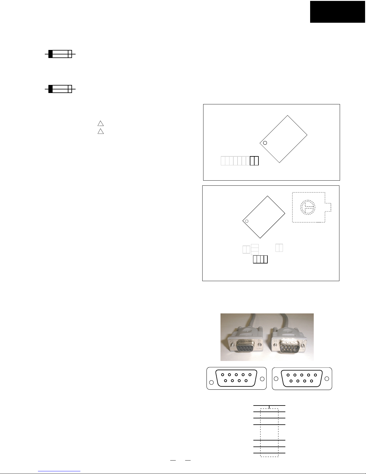
6. Connection of computer
When you change the program of microprocessor or control the unit
by the computer, connect the cable RS232C of straight type between
a computer and terminal RS232C on the rear panel.
12345
6789
54321
9876
To the unitTo PC
GND
GND
1
2
3
7
8
9
1
2
3
7
8
9
Page 4
RDC-7
4
Front panel facilities
Display
Here is an explanation of the controls and displays on the front panel of the RDC-7.
Front door
Front panel
Front panel door
Front panel display
ALDOLBY DIGIT
MPEG DTS
DOLBY
PROLOGIC
VIDEO
213
DVD
4 5 COMPONENT
ANALO G
DIGITAL
213
SLEEP
INPUT
Standby/On
Display DVD
Video
1
Video 2Video
3
Video
4
Video
5
Tape
1
Tape
2
AM
FM
Phono
C D
Open/Close
Zone
2
()
GRN
Rec
()
RED
Off
On
Standby
Master Volume
On
Power
AV Controller RDC-7
Phones
Clear
AV Controller
RDC-7
Digital format:
The current input source is set for
a digital format of ÒAuto.Ó
Bass level:
The current bass level is +2.
Treble level:
The current treble level is -2.
Front panel
Power
After plugging in the power cord into the rear panel and
wall outlet, pressing this button connects the RDC-7 to the
AC mains and turns it on.
¥
Before turning on the power, make sure all cables are
properly connected.
¥
Turning on the RDC-7 may cause a momentary power
surge that might interfere with other electrical equipment on the same circuit. If this is a problem, plug the
RDC-7 into a different electrical circuit.
Standby/On
Pressing this button while the main power is turned on the
STANDBY indicator lights up and the front display turns off.
Pressing it again returns it to the standby state. This state
turns off the display, disables control functions, and turns
off all outputs to the main zone (those for the remote zone
remain available).
On and Standby indicator
Master Volume
The MASTER VOLUME knob is used to control the volume
for the main zone. The volume for the remote zone (Zone
2) is independent.
Open/Close
Press this button to open and close the front door that
covers the lower buttons.
Display
The DISPLAY button is used to display information about
the current input source signal. Each time you press the
display button, the screen changes to show you different
information concerning the input signal.
The screen changes as follows:
Program format Sampling frequency Digital input
Digital format Bass level Treble level.
If the input source signal does not have any information
for a particular screen, then that screen will be skipped.
¥
Displaying the data of the current input source
Each display is explained below.
Program
format:
Front channel Surround channel
Sampling
frequency:
Source signal 48 kHz
Sampling frequency
Digital input:
The current input source is set for
digital input at OPT1.
LFE(Low Frequency Effect)
Input Source Buttons (DVD, VIDEO 1Ð
5, TAPE 1
Ð
2, AM, FM, PHONO, and CD) and Indicators
These buttons are used to select the input source for the
main zone. When an input source is selected, the indicator will light in blue. To select the input source for the remote zone (Zone 2) or recording out (Rec Out), first press
the Zone 2 or Rec Out button, and then the desired input
source button.
Zone 2/Rec Indicator
For Zone 2, the indicator above the selected input
source button will light green. For recording, it will light
red.
Lower buttons in the front door
Caution
:
The front door of the AV Controller is motorized. Use the
open/close button to open or close the door. Manually
opening or closing the door, or moving the AV Controller
while holding the door, will cause the door to malfunction
or break.
Rec Out
Press the Rec Out button to output to a recording component for recording purposes. After pressing the Rec Out
button, press one of the input source selector buttons
within 8 seconds to select the component to record to.
When one is selected, the indicator above that button will
light in red. To record from the same input source that you
are using (that is selected for the main zone), press the
Rec Out button twice in succession.
Note:
The Rec Out and Zone 2 buttons use the same circuit and
therefore cannot be used at the same time.
When Rec Out is selected, nothing is output from Zone 2.
Zone 2
The RDC-7 includes a second signal path separate from
the main one that can be used for a remote zone (Zone 2)
or for making recordings. By connecting an additional
amplifier or other video equipment to the Zone 2 outputs,
you can output to a separate room an input source that is
different from that being used in the main room. This allows you to watch one program in one room while somebody else is watching a different program in another.
Press the Zone 2 button to enable output to the ZONE 2
outputs. After pressing the Zone 2 button, press one of the
input source selector buttons within 8 seconds to select
the input source for the remote zone. When one is selected, the indicator above that button will light in green.
Page 5
RDC-7
5
Front panel facilities
Memory
This button only operates when FM or AM is selected as
the input source. This button allows you to preset frequencies for stations when using the FM/AM tuner. You
can preset up to 40 stations (or frequencies) to be used
with the PRESET buttons.
Menu, , , Enter, , , Exit
These buttons are used with the On Screen Display
(OSD) menu. They also perform the same functions as
the OSD MENU,
(upper edge of ENTER button),
(lower edge of ENTER button), (left edge of ENTER
button),
(right edge of ENTER button), ENTER, and EXIT
RETURN buttons on the remote controller.
Menu: Press to bring up the OSD menu.
Exit: Press to exit the OSD menu when at the Menu
Screen, or move to one screen previous to the one
that is displayed if at any other screen.
and : When selecting items in the OSD Menu, press
these buttons to move the on-screen cursor (or the
highlighted portion) upward and downward.
and : When setting parameters in the OSD menu,
press these buttons to select parameter values or
modes.
Enter: Press to display the screen for the selected item in
the OSD Menu.
Note for European models:
These buttons are also used to set programs and finish
scans when performing a PTY or TP scan with the RDS
broadcasts.
PHONES
This is a standard stereo jack for connecting stereo
headphones. The audio for the front right and left
speakers are sent to the headphone speakers. When
the headphones are plugged in, the listening mode
automatically changes to stereo and output to the
speakers is stopped.
Front panel display
Listening mode or digital input format
indicators
Multi function display
Sleep indicator
Input source format indicator
Video display
To use the same input source for the both the main and
remote zones, press the Zone 2 button twice in succession.
Note:
The Rec Out and Zone 2 buttons use the same circuit and
therefore cannot be used at the same time.
when Zone 2 is selected, the currently selected input
source is output from the recording terminal.
Off
When not using either Rec Out or Zone 2, press that button and then press the Off button to turn off the signal.
If the Rec Out or Zone 2 signal is turned on and the connected component is not turned on, the electric signal
will still be sent through the circuitry and the excess
load may cause deterioration of the audio signal.
DSP
Press these buttons to scroll through the listening modes
and set a new one for the input source you are currently listening to. For each different input signal, different listening modes are possible.
Dimmer (other than European models)
Press to set the brightness of the front display. There are
4 settings available: normal, dark, very dark, and off.
¥ The dimmer control for the front display can be per-
formed at the remote controller.
RT/PTY/TP (European models only)
This button is only available on European models. Use
this button to help tune into the Radio Data System
(RDS) for FM broadcasting. RDS was developed within
the European Broadcasting Union (EBU) and is available in most European countries. Each time the button
is pressed, the display changes from RT (radio text) to
PTY (program type) to TP (traffic program) and then
back to RT again.
Tuning
Use these buttons to change the tuner frequency. The
tuner frequency is displayed in the front display and it
can be changed in 50 kHz increments for FM and 9 kHz
increments for AM. When a station is tuned into,
Ò> <Ó or Ò
Ó will appear in the front display.
When FM is selected, you can hold down one of the
tuning buttons and then release it to activate the autosearch feature. It will search for a station in the direction of the button you pressed and stop when it tunes
into one.
Preset
When AM or FM is selected as the input source, press
one of these buttons to jump to a radio station that you
preset using the MEMORY button. Pressing the right button moves from the most recently preset station to
older ones, and pressing the left button moves in the
reverse order.
FM Mode
If you are listening to an FM radio station in stereo and
the sound cuts out or there is a great deal of noise, then
press this button. The ÒMONO Ó display will appear and
the output will change to mono. Though you will not
hear the audio in stereo, this may stop the sound from
cutting out and reduce excess noise.
Remote controller
SEND/LEARN indicator
Lights red when a signal is emitted from the
remote controller.
LCD display
Displays the input and operating status.
ON
Turns on the RDC-7.
SLEEP
Sets the sleep function.
DIRECT MACRO
Programming or running a direct macro
function.
MODE buttons
Sets the remote controller into the mode for the
device corresponding to the button pressed.
DISPLAY
Changes the display.
DVD SET
Brings up the DVD setup menu when the DVD
mode is selected.
CH
Selects the tuner preset stations.
EXIT
Set the new settings and return to the previous
menu screen.
RETURN
Returns to the DVD menu screen when the DVD
mode is selected.
TRACK
Selects a CD track when the CD mode is
selected.
CD/TAPE/DVD/MD operation buttons
Operates other Onkyo and Integra components.
Input Selector buttons
Selects an input source.
DVD: DVD, CD:CD,T1:Tape1, T2:Tape2, TUN:AM/
FM, PH:Phono, V1:Video1, V2:Video2, V3:Video3,
V-: Use this button in conjunction with a numeric
button to select Video 1 through 5.
1-9, 0, +10
Numeric key. The +10 button changes the value
of the 10's digit.
Re-EQ
Selects the Re-EQ mode.
LATE NIGHT
Selects the late night mode.
DIMMER
Adjusts the display brightness.
STNBY
Turns the RDC-7 in standby. Be aware that
pressing the STNBY button only places the RDC-7
in standby and does not turn the power
completely off.
LIGHT
Illuminates the buttons.
MODE MACRO
Programming or running a macro function.
OSD
Brings up the OSD menu.
MENU
Displays the menu when the DVD mode is
selected.
ENTER/cursor
VOL
Adjusts the volume.
TEST
Outputs a test tone for setting speaker levels.
TV/VCR
Used to program the signals from remote
controllers for other components. Program the
TV/VCR switching mode.
MUTING
Activate the mute function.
DISC
Selects a disc in the CD changer when the CD
mode is selected.
OPEN/CLOSE
Open and close the front door.
Listening mode buttons
Pressing these buttons to change the listening
mode directly.
Speaker output level setting buttons
Use to set the speaker output levels.
ENT
Enters numerical values and settings when either
the MD or DVD mode is selected.
OPEN/COLSEREC
AUDIO MUTING
DISCTRACK
DVD
CD
PH
TUN
T2T1
V1
STEREO
123
654
7
+
10 0
ENT
89
SURROUND THX DSP
LEVEL
+
CH SELRe-EQ
LEVEL
Ð
DIMMERLATE NIGHT
DIRECT DSP
V2 V3 V
Ð
HOME THEATER CONTROLLER
RC-418M
Page 6
RDC-7
6
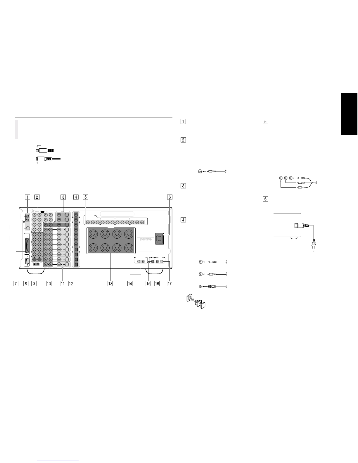
Rear panel facilities
Improper connection
Inserted completely
Here is an explanation of the terminals found on the
rear of the RDC-7 and how they are used. Before
connecting your audio and video components, be
sure to read this section carefully and then proceed
to the explanations on how to connect each individual component.
¥ Be sure to always refer to the instructions that came
with the component that you are connecting.
¥ Do not plug in the power cord until all connections
have been made.
¥ For input jacks, red connectors (marked R) are used
for the right channel, white connectors (marked L)
are used for the left channel, and yellow connectors
(marked V) are used for video connection.
¥ Insert all plugs and connectors securely. Improper
connections can result in noise, poor performance,
or damage to the equipment.
¥ Do not bind audio/video connection cables with
power cords and speaker cables. Doing so may
adversely affect the picture and sound quality.
DVD
VIDEO
5
VIDEO
4
VIDEO
3
ZONE 2
MONITOR
OUT
VIDEO
1
VIDEO
2
R
L
R
L
C
SUBWOOFER
IR IN
MAIN ZONE 2
VIDEO
S VIDEO
VIDEO
S VIDEO
INPUT 2
P
BPR
Y
INPUT 3
PBPRY
OUTPUT
PBPRY
OUT
OUT
IN
IN
IN
IN
IN
IN
AC
INLET
OUT
1
2
FM
ANT.
75
AM
ANT.
C D
GND
MULTI
CHANNEL
INPUT
RS232
TAPE
2
TAPE
1
FRONT
3
2
1
3
2
5
4
1
I N
I
N
I
N
I
N
OUT
OUT
L
R
L
1212121
2
R
COMPONENT
VIDEO
INPUT 1
P
BPR
Y
DIGITAL
OUTPUT
(
COAXIAL
)
AC-3
RF
DIGITAL
INPUT
(
COAXIAL
)
DIGITAL
OUTPUT
(
OPTICAL
)
DIGITAL
INPUT
(
OPTICAL
)
PHONO
SURR
BACK
SURR
PRE
OUT
RIGHT CENTER SUBWOOFER
SURROUND
RIGHT
SURROUND
LEFT
SURROUND BACK
RIGHT
SURROUND BACK
LEFT
LEFT
PRE OUT
AV CONTROLLER
MODEL NO.
RDC-7
12V TRIGGER
AB
COMPONENT VIDEO INPUT/OUTPUT
If your DVD player or other device has component
video connectors, be sure to connect them to these
component video connectors on the RDC-7. The RDC7 has three component video input connectors to obtain the color information (Y, P
B, PR) directly from the
recorded DVD signal or other video component and
one component video output connector to output it
directly into the matrix decoder of the display device.
By sending the pure DVD component video signal directly, the DVD signal forgoes the extra processing that
normally would degrade the image. The result is vastly
increased image quality, with incredibly lifelike colors
and crisp detail.
YPB PR RCA type
¥ When using the digital inputs and outputs, make
sure to also connect the analog connections whenever possible.
¥ When using one of the optical input or output jacks,
remove the protective cap and keep it safely.
When the jack is not used, replace the protective
cap.
¥ When using an optical input or output jack, always
use an optical fiber cable.
RCA type
COAXIAL Coaxial cable
AC-3RF Coaxial cable
OPTICAL Optical fiber cable
Optical digital input terminal
An optical digital input terminal is
equipped with a protection cap.
When connecting, remove this cap.
When not using, put the cap back
on the terminal.
Power cord
(supplied)
To an AC
wall outlet
AC INLET
Plug the supplied power cord into this AC INLET and
then into the power outlet on the wall.
¥ Do not use a power cord other than the one sup-
plied with the RDC-7. The power cord supplied is
designed for use with the RDC-7 and should not be
used with any other device.
¥ Never have the power cord disconnected from the
RDC-7 while the other end is plugged into the wall
outlet. Doing so may cause an electric shock. Always connect by plugging into the wall outlet last
and disconnect by unplugging from the wall outlet
first.
ANTENNA
These jacks are for connecting the FM indoor antenna
and AM loop antenna that are supplied with the RDC-
7.
PRE OUT (RCA type)
These jacks are for connecting power amplifiers. If the
jacks on your power amplifier are RCA type jacks, connect them here. Two terminals are provided for each of
the front left, center, and right channels. The same signal is output from both terminals 1 and 2.
DIGITAL INPUT/OUTPUT
(coaxial, optical, and input-only AC-3RF)
These are the digital audio inputs and outputs. There
are 5 digital inputs with coaxial jacks, 3 with optical
jacks, and 1 AC-3RF input. The inputs accept digital
audio signals from a compact disc, LD, DVD, or other
digital source component. For digital output, there is 1
coaxial output and 1 optical output. The digital outputs
can be connected to MD recorders, CD recorders, DAT
decks, or other similar components.
MONITOR OUT
There are 2 monitor outputs and each one includes
both composite video and S-video configurations.
When connecting two video monitors or televisions, be
aware that the OSD interface can only be used with
MONITOR OUT 1 (OSD will not be displayed on the
video monitor connected to MONITOR OUT 2).
Page 7
RDC-7
7
MULTI
CHANNEL
INPUT
(Green)
(Blue)
(Red)
(Brown)
(Black)
(Yellow)
Tighten locking
screws
Front left
DVD player or MPEG decoder
Front right
Center
Surround right
Surround left
Subwoofer
RDC-7 MULTI CHANNEL INPUT
(DB-25-type terminal)
DB-25 to
RCA 6-ch cable
(supplied)
Rear panel facilities
¥ When using the PHONO jacks, remove the caps that
cover then and store them safely where they will not
be lost. Whenever the PHONO jacks are not in use,
replace the caps on them.
¥ When connecting a VCR or other video compo-
nent, make sure you connect the audio and video
leads together (i.e., both to VIDEO 3).
¥ With LD players that have an AC-3RF terminal, con-
nect the audio source to the audio inputs of VIDEO
4 because only it supports the AC-3RF settings during digital setup.
¥ The RDC-7 is designed for use with turntables that
use moving magnet cartridges.
MULTI CHANNEL INPUT
By connecting a DVD player, MPEG decoder, or other
component that has a multi channel port, you can
playback the audio with 5.1 channel or 7.1 channel
output. So, be sure to prepare a cable that can properly connect the RDC-7 to the peripheral device.
RS 232
The RS 232 port is to be used in conjunction with an external controller to control the operation of the RDC-7
by using an external device. The RS 232 port may also
be used in the future to update the operating software
of the RDC-7 so that it will be able to support new digital audio formats and the like as they are introduced.
GND
Use this GND terminal for connecting the ground (or
earth) wire if a turntable is connected.
AUDIO IN/OUT
These are the analog audio inputs and outputs. There
are 10 audio inputs (6 of which are linked to video inputs) and 4 audio outputs (2 of which are linked to
video outputs). The audio jacks are nominally labeled
for cassette tape decks, compact disc players, turntables, and DVD players. To the audio jacks for VIDEO 1
to 5, connect the audio output from VCRs, LD players,
and other video components. The audio inputs and
outputs require RCA-type connectors.
The MULTI CHANNEL INPUT is a DB-25 port and the RDC7 is equipped provided with a DB-25-to-RCA 6-channel
cable. When making a multi-channel connection to a
DVD player or MPEG decoder, connect the DB-25 end
of the cable to the MULTI CHANNEL INPUT port on the
RDC-7 and RCA-type ends to the ends of the cables
connected to the other component. The channel colors are shown below.
Front left (Blue)
Front right (Red)
Center (Green)
Surround left (Black)
Surround right (Yellow)
Subwoofer (Brown)
If the DVD player or MPEG decoder that you are connecting to is provided with DB-25-to-DB-25 cable, then
connect that directly to the RDC-7 and do not use the
cable supplied with the RDC-7.
When connecting the cable, be sure to secure the
locking screws on the DB-25 connectors.
VIDEO IN/OUT
These are the video inputs and outputs. There are 6
video inputs and 2 video outputs and each one includes both composite video and S-video configurations. Connect VCRs, LD players, DVD players, and
other video components to the video inputs. S-video
sources can be viewed via the S-video or composite
outputs, while composite sources can only be viewed
through the composite output.
The 2 video output channels can be used to be connected to video tape recorders for making recordings.
Composite video jack
S video jack
¥ When connecting a VCR or other video compo-
nent, make sure you connect the audio and video
leads together (i.e., both to VIDEO 3).
¥ With LD players that have an AC-3RF terminal, con-
nect the video source to the video inputs of VIDEO 4
because only it supports the AC-3RF settings during
digital setup.
RCA type
IR IN MAIN
If the RDC-7 is located inside a rack or cabinet that will
not allow infrared beams to reach the IR sensor, you will
need to connect a remote sensor* to this input to be
able to use the remote controller. Then install the remote sensor in an unblocked location where you can
easily point the remote controller.
* An optional remote sensor kit is required.
IR IN ZONE 2
This jack allows you to connect a multiroom system kit
so that you can use the remote controller while you are
in the remote zone (Zone 2), which may be far separated from the RDC-7.
* To be able to use the remote controller in the remote
zone (Zone 2), you must connect one of the following (sold separately):
¥ Integra Õs Multi-Room System Kit (IR Remote Control-
ler Extension System).
¥ A multiroom A/V distribution and control system
from Niles , Xantech , or the like.
ZONE 2
These are the audio and video output jacks for the remote zone (Zone 2). Use these outputs to connect the
remote zone.
PRE OUT (Balanced type)
These jacks are for connecting power amplifiers. If the
jacks on your power amplifier are XLR (balanced) type
jacks, connect them here. The pin assignments for
these terminals are shown below.
12V TRIGGER
This is a 12-volt output terminal so that the RDC-7 can
control other external devices. For other devices that
have an input terminal of the same kind, you can connect it to this terminal with 1/8-inch mini-jack cable so
that its power is turned on when you press an input
source button. The RDC-7 is equipped with two 12-volt
trigger terminals and each supplies a current of 100
mA. When you connect to either of these terminals,
make the appropriate settings in the OSD menu.The initial settings are ÒA: On Ó and ÒB: Off,Ó so if you are only
connecting to A, these settings will not need to be
changed.
(RI)
By connecting the connector as shown in the diagram below, you can use the RC-418M remote controller to operate Integra/Onkyo cassette tape decks and
compact disc players that also have Integra/OnkyoÕs
connectors. Simply connect a remote control cable
from this connector to the connector of the cassette tape deck or compact disc player. An remote
control cable with a 3.5-mm (1/8-inch) miniature twoconductor plug comes with every cassette tape deck
and compact disc player that has an connector.
¥ For remote control operation, the audio connection
cables must also be connected.
¥ The RC-418M remote controller does not support
turntables.
¥ If the connected component has two connec-
tors, you can use either one to connect to the RDC-
7. The other one can be used to daisy chain with
another component.
¥ For Integra DVD or MD players, you can control
them by simply pointing the RC-418M controller directly at the component.
Ex:Integra/Onkyo
CD player
Ex:Onkyo
Cassette tape deck
RDC-7
connector
connector
These pin assignments conform to the standards made
by the Audio Engineering Society. Check the instruction manual that came with your power amplifier and
verify that the input pin assignments are compatible
with those for the RDC-7.
1. GND
Balanced cableXLR type
2. non-inverting (+)
3. inverting (-)
1. Connecting the output terminal
Match the pins and insert the terminal until you hear a
Òclick. Ó Ensure that it is secure by gently pulling it.
2. Disconnecting tha output terminal
Pull out the cable (in the direction indicated by the
arrow) while holding down the connection cable button.
Push
These outputs are activated by the Zone 2
button on
the front panel.
R
R
RI
RI
RI
RI
RI
RI
RI
RI
Page 8
RDC-7
8
AM
ANT.
FM
ANT.
75
MULTI
CHANNEL
INPUT
RS232
GND
C
FRONT
R
L
SURR
BACK
SURR
SUBWOOFER
1212121
2
PRE
OUT
DVD
VIDEO
5
VIDEO
4
VIDEO
3
ZONE 2
MONITOR
OUT
VIDEO
1
VIDEO
2
R
L
R
L
VIDEO
S VIDEO
VIDEO
S VIDEO
INPUT 2
P
BPR
Y
INPU
T
PBY
OUT
OUT
IN
IN
IN
IN
IN
IN
OUT
1
2
C D
TAPE
2
TAPE
1
3
2
1
3
2
5
4
1
I N
I
N
I
N
I
N
OUT
OUT
L
R
COMPONENT
VIDEO
INPUT 1
P
BPR
Y
DIGITAL
OUTPUT
(
COAXIAL
)
AC-3
RF
DIGITAL
INPUT
(
COAXIAL
)
DIGITAL
OUTPUT
(
OPTICAL
)
DIGITAL
INPUT
(
OPTICAL
)
PHONO
RIGHTRIGHT CENTER
CENTER SUBWOOFER
SURROUNDSURROUND
RIGHTRIGHT
SURROUND
SURROUND
LEFTLEFT
SURROUND BACK
SURROUND BACK
RIGHT
RIGHT
SURROUND BACK
LEFT
LEFTLEFT
PRE OUTPRE OUT
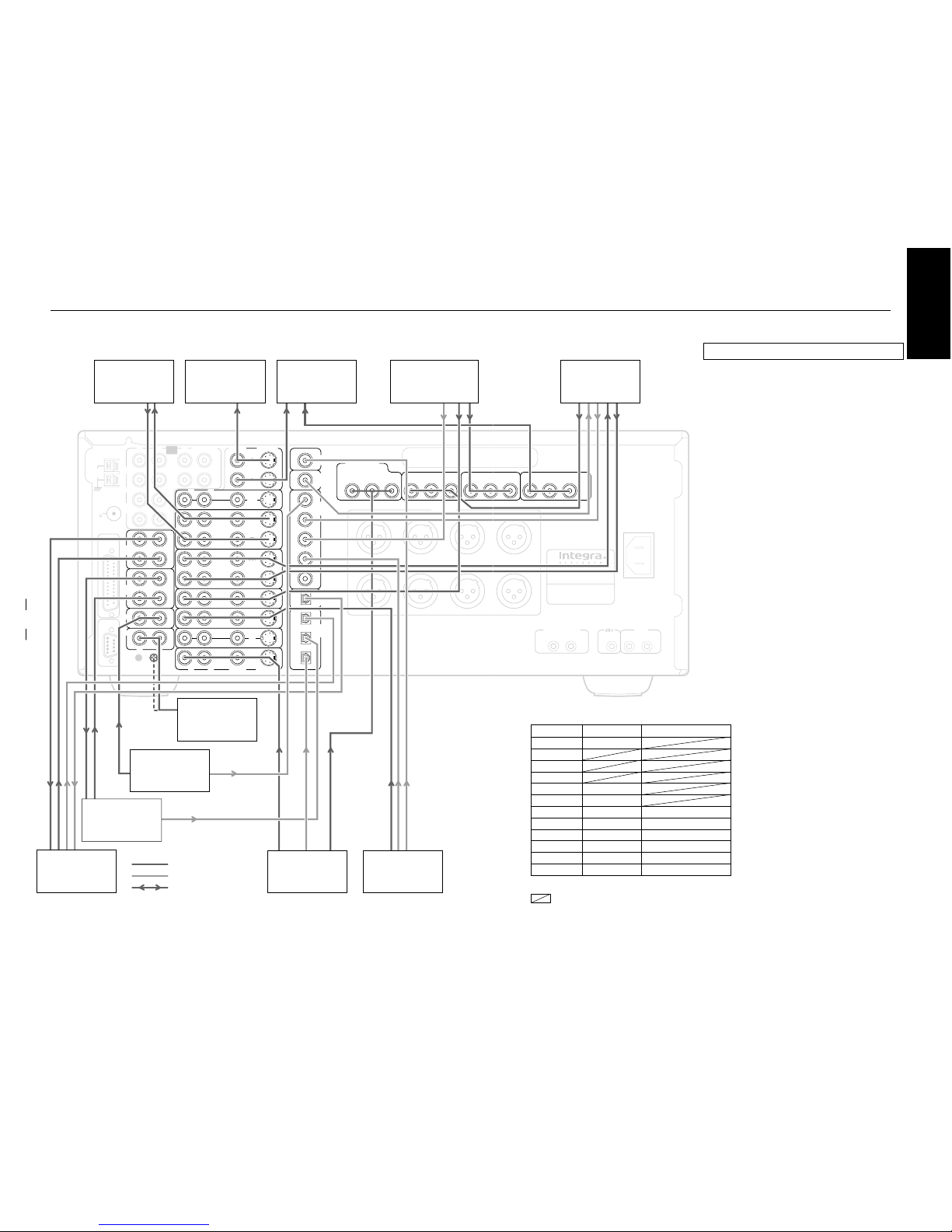
Example of how to connect your equipment
VCR
(VIDEO 1)
TV monitor
(MONITOR OUT 1)
Projector
(MONITOR OUT 2)
Cable/Satellite
(Set top box, VIDEO 3)
DAT deck, CD-R,
MD recorder
(TAPE 1)
Tape deck, DAT,
MD recorder, CD-R
(TAPE 2)
CD player
(CD)
Turntable
(PHONO)
DVD player
(DVD)
LD player
(VIDEO 4)
Analog signal
Digital signal
flow
IR IN
AC
INLET
MAIN ZONE 2
T
3
P
R
OUTPUT
P
BPR
Y
SUBWOOFER
SUBWOOFER
SURROUND BACKSURROUND BACK
LEFTLEFT
AV CONTROLLER
MODEL NO. RDC-7
12V TRIGGER
AB
Default setting
Input source Digital input Component video
CD COAXIAL 1
PHONO
FM
AM
TAPE 1 OPTICAL 1
TAPE 2 OPTICAL 2
DVD OPTICAL 3
COMPONENT VIDEO 1
VIDEO 1 ---- ----
VIDEO 2 COAXIAL 2
COMPONENT VIDEO 2
VIDEO 3 COAXIAL 3
COMPONENT VIDEO 3
VIDEO 4 COAXIAL 4 ----
VIDEO 5 COAXIAL 5 ----
DVD recorder
or other digital video
recording device
----
: No setting
: No applicable
Standard connections
Here is explanation of how to connect the main
components to the RDC-7 in the standard manner.
There are many ways that any one component can be
connected, and it is up to you to decide which method
best fits your situation. The directions given here are
only one option and should only be thought of as such.
It is best to fully understand the nature of each
connector and terminal as well as each of your
components and their features to ascertain which
method of connection is best.
¥ Be sure to always refer to the instruction manual that
came with the component that you are connecting.
¥ Do not plug in the power cord until all connections
have been made.
¥ For input jacks, red connectors (marked R) are used
for the right channel, white connectors (marked L)
are used for the left channel, and yellow connectors
(marked V) are used for video connection.
¥ Insert all plugs and connectors securely. Improper
connections can result in noise, poor performance,
or damage to the equipment.
¥ Do not bind audio connection cables with power
cords and speaker cables. Doing so may adversely
affect the sound quality.
Connecting power amplifiers:
Speaker configuration and placement:
Radio antenna:
Enjoying the RDC-7 from a remote room (Zone 2):
Page 9

RDC-7
9
Example of how to connect your equipment
Connecting your audio components
Below is an example of how you can connect your
audio components to the RDC-7.
1. Connecting a turntable
Using an RCA-type audio connection cable, connect
the output terminal on the turntable to the PHONO IN
jacks on the RDC-7. Make sure that you properly connect the left channel to the L jack and the right channel to the R jack.
Note:
The RDC-7 is designed for use with moving magnet cartridges. For proper operation, connect a ground (or
earth) wire to the GND terminal. For some turntables,
however, connecting the ground wire may cause increased noise, and in such a case, a ground wire is not
necessary and should not be connected.
2. Connecting a compact disc player
Using an RCA-type audio connection cable, connect
the output terminal on the compact disc player to the
CD IN jacks on the RDC-7. Make sure that you properly
connect the left channel to the L jack and the right
channel to the R jack.
If the compact disc player has a digital output jack as
well, be sure to also connect it to either a DIGITAL INPUT
(COAXIAL) or DIGITAL INPUT (OPTICAL) jack on the
RDC-7 depending on the type of connector on the
compact disc player.
With the initial settings of the RDC-7, the CD input
source is set for digital input at the COAXIAL 1 jack. If
the digital connection is made at a different jack, this
must be changed at the OSD Menu: Input Setup
Digital Setup Digital Input .
3. Connecting a cassette tape deck, MD
recorder, DAT deck, or CD recorder
Using an RCA-type audio connection cable, connect
the output terminals (PLAY) of the device to the TAPE 2
IN jacks on the RDC-7 and the input terminals (REC) to
the TAPE 2 OUT jacks. Make sure that you properly connect the left channel to the L jack and the right channel to the R jack.
If the device has a digital output jack as well, be sure to
also connect it to either a DIGITAL INPUT (COAXIAL) or
DIGITAL INPUT (OPTICAL) jack on the RDC-7 depending
on the type of connector on the device.
With the initial settings of the RDC-7, the TAPE 2 input
source is set for digital input at the OPTICAL 2 jack. If the
digital connection is made at a different jack, this must
be changed at the OSD Menu: Input Setup Digital
Setup Digital Input .
If the device also has a digital input jack, it can be connected to the DIGITAL OUTPUT (COAXIAL) or DIGITAL
OUTPUT (OPTICAL) jack on the RDC-7 for recording of
the signal from the input source selected at the RDC-7.
4. Connecting an MD recorder, DAT deck, or CD
recorder
Using an RCA-type audio connection cable, connect
the output terminals (PLAY) of the device to the TAPE 1
IN jacks on the RDC-7 and the input terminals (REC) to
the TAPE 1 OUT jacks. Make sure that you properly connect the left channel to the L jack and the right channel to the R jack.
If the device has a digital output jack as well, be sure to
also connect it to either a DIGITAL INPUT (COAXIAL) or
DIGITAL INPUT (OPTICAL) jack on the RDC-7 depending
on the type of connector on the device.
With the initial settings of the RDC-7, the TAPE 1 input
source is set for digital input at the OPTICAL 1 jack. If the
digital connection is made at a different jack, this must
be changed at the OSD Menu: Input Setup
Digital
Setup Digital Input.
If the device also has a digital input jack, it can be connected to the DIGITAL OUTPUT (COAXIAL) or DIGITAL
OUTPUT (OPTICAL) jack on the RDC-7 for recording of
the signal from the input source selected at the RDC-7.
Connecting your video components
Below is an example of how you can connect your
video components to the RDC-7.
The flow of the video signals is as follows: the signal that
comes in from VIDEO IN is sent to VIDEO OUT, the signal
that comes in from S-VIDEO IN is sent to S-VIDEO OUT
and VIDEO OUT, and the signal that comes in from
COMPONENT VIDEO IN is sent to COMPONENT VIDEO
OUT.
If only the video connection for the MONITOR OUT is
made, even if the input from each source component
is through a component video connection, the picture
will not appear. If only the S-video connection for the
MONITOR OUT is made, the picture will not appear.
5. Connecting a DVD player
Using an RCA-type video connection cable, connect
the video output terminal (composite) on the DVD
player to the DVD VIDEO IN jack on the RDC-7. If there is
an S-video output terminal on the DVD player, connect
it to the DVD S VIDEO IN jack using an S-video cable. If
the DVD player has component video outputs, connect them to one of the COMPONENT VIDEO INPUT
jacks.
Using an RCA-type audio connection cable, connect
the audio output terminal on the DVD player to the audio DVD IN jacks on the RDC-7. Make sure that you
properly connect the left channel to the L jack and the
right channel to the R jack.
If the DVD player has a digital output jack as well, be
sure to also connect it to either a DIGITAL INPUT (COAXIAL) or DIGITAL INPUT (OPTICAL) jack on the RDC-7
depending on the type of connector on the DVD
player.
With the initial settings of the RDC-7, the DVD input
source is set for digital input at the OPTICAL 3 jack. If the
digital connection is made at a different jack, this must
be changed at the OSD Menu: Input Setup Digital
Setup Digital Input .
9. Connecting a DVD recorder or other digital
video recording device
Using an RCA-type video connection cable, connect
the video output terminal (composite) on the device to
the VIDEO 2 IN jacks on the RDC-7 and video input terminal to the VIDEO 1 OUT jacks. If there is an S-video
input/output terminal on the device, connect it to the S
VIDEO 2 IN/OUT jack using an S-video cable. If the device has component video outputs, connect them to
one of the COMPONENT VIDEO INPUT jacks.
Using an RCA-type audio connection cable, connect
the audio output terminal on the device to the same
VIDEO 2 IN audio jacks on the RDC-7 and audio input
terminal to the VIDEO 1 OUT audio jacks. Make sure
that you properly connect the left channel to the L jack
and the right channel to the R jack.
If the device has a digital output jack as well, be sure to
also connect it to either a DIGITAL INPUT (COAXIAL) or
DIGITAL INPUT (OPTICAL) jack on the RDC-7 depending
on the type of connector on the device.
With the initial settings of the RDC-7, the VIDEO 2 input
source is set for digital input at the COAXIAL 2 jack. If
the digital connection is made at a jack different from
the initial settings, this must be changed at the OSD
Menu: Input Setup Digital Setup Digital Input.
If the device also has a digital input jack, it can be connected to the DIGITAL OUTPUT (COAXIAL) or DIGITAL
OUTPUT (OPTICAL) jack on the RDC-7 for recording of
the signal from the input source selected at the RDC-7.
10. Connecting a television monitor or projector
Using an RCA-type video connection cable, connect
the video input terminal (composite) on the monitor to
one of the MONITOR OUT jacks on the RDC-7. If there is
an S-video input terminal on the monitor, connect it to
the S VIDEO MONITOR OUT jack using an S-video cable.
If the device has component video inputs, connect
them to the COMPONENT VIDEO OUTPUT jacks.
Note that the OSD Menu will not be displayed on the
monitor connected to MONITOR OUT 2. This allows you
to connect large screens or projectors to MONITOR OUT
2 and use a smaller television connected to MONITOR
OUT 1 just to make settings in the OSD Menu.
6. Connecting a LD player
Using an RCA-type video connection cable, connect
the video output terminal (composite) on the LD player
to the VIDEO 4 IN jack on the RDC-7. If there is an Svideo output terminal on the LD player, connect it to
the S VIDEO 4 IN jack using an S-video cable.
If the LD player has an AC-3RF output, connect it to the
AC-3RF jack on the RDC-7. If this connection is made,
ÒAC-3RFÓ must be set in the OSD Menu: Input Setup
Digital Setup Digital Format.
Using an RCA-type audio connection cable, connect
the audio output terminal on the LD player to the audio
VIDEO 4 IN jacks on the RDC-7. Make sure that you
properly connect the left channel to the L jack and the
right channel to the R jack.
If the LD player has a digital output jack as well, be sure
to also connect it to either a DIGITAL INPUT (COAXIAL)
or DIGITAL INPUT (OPTICAL) jack on the RDC-7 depending on the type of connector on the LD player.
With the initial settings of the RDC-7, the VIDEO 4 input
source is set for digital input at the COAXIAL 4 jack. If
the digital connection is made at a different jack, this
must be changed at the OSD Menu: Input Setup
Digital Setup Digital Input.
7. Connecting a video cassette recorder
Using an RCA-type video connection cable, connect
the video output terminal (composite) on the video
cassette recorder to the VIDEO 1 IN jacks on the RDC-7
and video input terminal to the VIDEO 1 OUT jacks. If
there is an S-video input/output terminal on the video
cassette recorder, connect it to the S VIDEO 1 IN/OUT
jack using an S-video cable. If the video cassette recorder has component video outputs, connect them
to one of the COMPONENT VIDEO INPUT jacks.
Using an RCA-type audio connection cable, connect
the audio output terminal on the video cassette recorder to the same VIDEO 1 IN audio jacks on the RDC7 and audio input terminal to the VIDEO 1 OUT audio
jacks. Make sure that you properly connect the left
channel to the L jack and the right channel to the R
jack.
8. Connecting a satellite tuner or television
Using an RCA-type video connection cable, connect
the video output terminal (composite) on the satellite
tuner or television to the VIDEO 3 IN jacks on the RDC-7.
If there is an S-video output terminal on the satellite
tuner or television, connect it to the S VIDEO 3 IN jack
using an S-video cable. If the satellite tuner or television
has component video outputs, connect them to one of
the COMPONENT VIDEO INPUT jacks.
Using an RCA-type audio connection cable, connect
the audio output terminal on the satellite tuner or television to the same VIDEO 3 IN audio jacks on the RDC-7.
Make sure that you properly connect the left channel
to the L jack and the right channel to the R jack.
If the satellite tuner or television has a digital output
jack as well, be sure to also connect it to either a DIGITAL INPUT (COAXIAL) or DIGITAL INPUT (OPTICAL) jack
on the RDC-7 depending on the type of connector on
the set top box or television.
With the initial settings of the RDC-7, the VIDEO 3 input
source is set for digital input at the COAXIAL 3 jack. If
the digital connection is made at a jack different from
the initial settings, this must be changed at the OSD
Menu: Input Setup Digital Setup Digital Input.
Page 10
RDC-7
10
AC
INLET
AM
ANT.
FM
ANT.
75
MULTI
CHANNEL
INPUT
RS232
GND
VIDEO
S VIDEO
DVD
VIDEO
5
VIDEO
4
VIDEO
3
MONITOR
OUT
VIDEO
1
VIDEO
2
OUT
IN
IN
IN
IN
IN
IN
OUT
R
L
VIDEO
S VIDEO
C
D
TAPE
2
TAPE
1
I N
I
N
I
N
I
N
OUT
OUT
L
R
PHONO
3
2
1
3
2
5
4
1
DIGITAL
OUTPUT
(
COAXIAL
)
AC-3
RF
DIGITAL
INPUT
(
COAXIAL
)
DIGITAL
OUTPUT
(
OPTICAL
)
DIGITAL
INPUT
(
OPTICAL
)
INPUT 2
P
BPR
Y
INPUT 3
PBPRY
OUTPUT
PBPRY
COMPONENT
VIDEO
INPUT 1
P
BPR
Y
1
2
IR IN
MAIN ZONE 2
12V TRIGGER
AB
ZONE 2
R
L
OUT
C
FRONT
R
L
SURR
BACK
SURR
SUBWOOFER
1212121
2
PRE
OUT
RIGHT CENTER SUBWOOFER
SURROUND
RIGHT
SURROUND
LEFT
SURROUND BACK
RIGHT
SURROUND BACK
LEFT
LEFT
PRE OUT
AV CONTROLLER
MODEL NO.
RDC-7
RIGHT CENTER SUBWOOFER
SURROUND
RIGHT
SURROUND
LEFT
SURROUND BACK
RIGHT
SURROUND BACK
LEFT
LEFT
PRE OUT
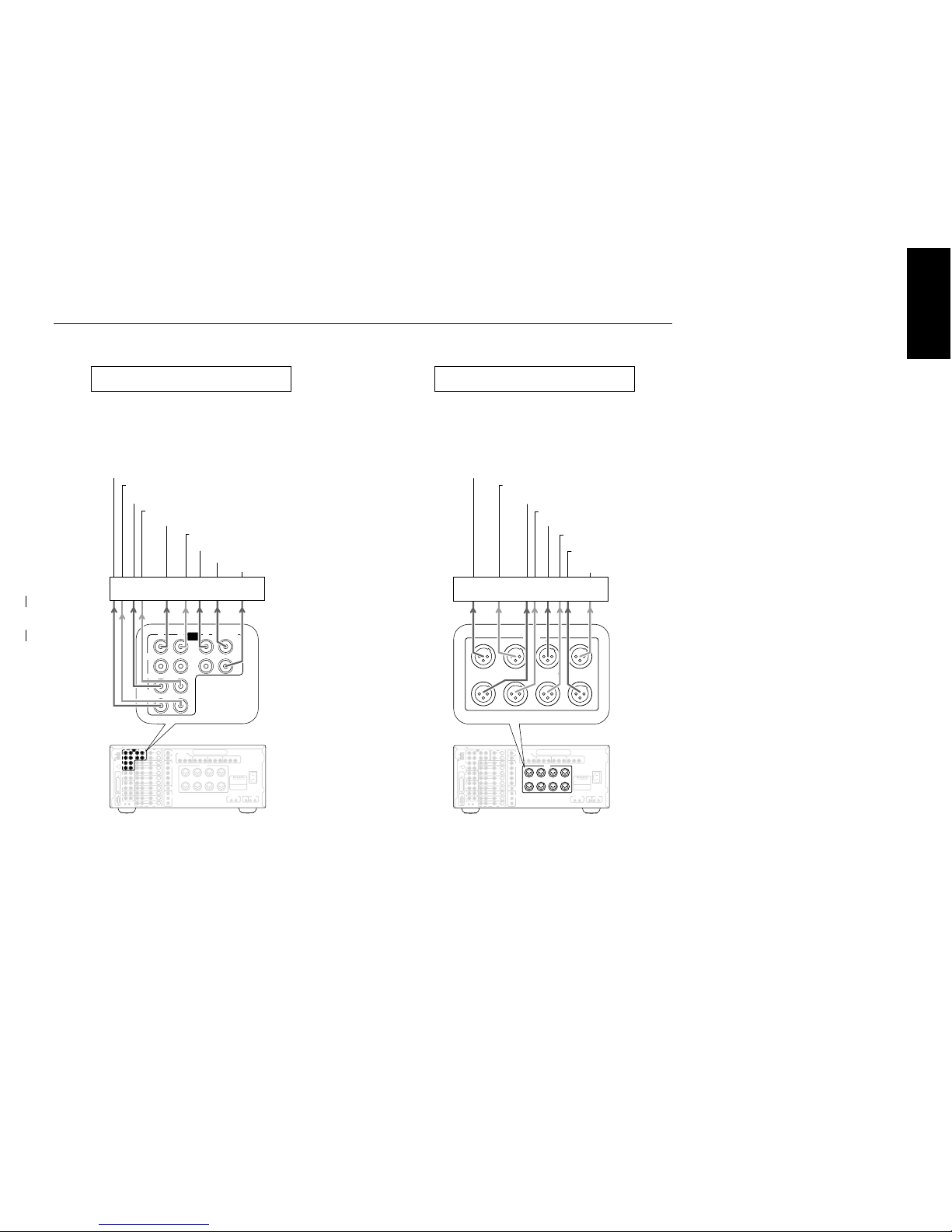
Connecting power amplifier s
Connecting power amplifiers with RCA type
connector
Connect your power amplifier to the PRE OUT jacks on
the RDC-7. If the jacks on your power amplifier are RCA
type jacks, connect them to the jacks shown in the
diagram given below. Two terminals are provided for
each of the front left, center, and right channels. The
same signal is output from both terminals 1 and 2.
Connecting power amplifiers with XLR type
connector
Connect your power amplifier to the PRE OUT jacks on
the RDC-7. If the jacks on your power amplifier are XLR
(balanced) type jacks, connect them to the jacks
shown in the diagram given below.
AC
INLET
AM
ANT.
FM
ANT.
75
MULTI
CHANNEL
INPUT
RS232
GND
VIDEO
S VIDEO
DVD
VIDEO
5
VIDEO
4
VIDEO
3
MONITOR
OUT
VIDEO
1
VIDEO
2
OUT
IN
IN
IN
IN
IN
IN
OUT
R
L
VIDEO
S VIDEO
C
D
TAPE
2
TAPE
1
I N
I
N
I
N
I
N
OUT
OUT
L
R
PHONO
3
2
1
3
2
5
4
1
DIGITAL
OUTPUT
(
COAXIAL
)
AC-3
RF
DIGITAL
INPUT
(
COAXIAL
)
DIGITAL
OUTPUT
(
OPTICAL
)
DIGITAL
INPUT
(
OPTICAL
)
INPUT 2
P
BPR
Y
INPUT 3
PBPRY
OUTPUT
PBPRY
COMPONENT
VIDEO
INPUT 1
P
BPR
Y
1
2
IR IN
MAIN ZONE 2
12V TRIGGER
AB
ZONE 2
R
L
OUT
C
FRONT
R
L
SURR
BACK
SURR
SUBWOOFER
1212121
2
PRE
OUT
RIGHT CENTER SUBWOOFER
SURROUND
RIGHT
SURROUND
LEFT
SURROUND BACK
RIGHT
SURROUND BACK
LEFT
LEFT
PRE OUT
AV CONTROLLER
MODEL NO.
RDC-7
C
FRONT
R
L
SURR
BACK
SURR
1212121
2
SUBWOOFER
PRE
OUT
Power amplifier
Front right speaker
Front left speaker
Subwoofer
Center speaker
Surround right speaker
Surround left speaker
Surround back right speaker
Surround back left speaker
RDC-7
Subwoofer
Center speaker
Surround back right
speaker
Subwoofer
Surround back left
speaker
Surround right speaker
Surround left speaker
Front right speaker
Front left speaker
Power amplifier
Page 11
RDC-7
11
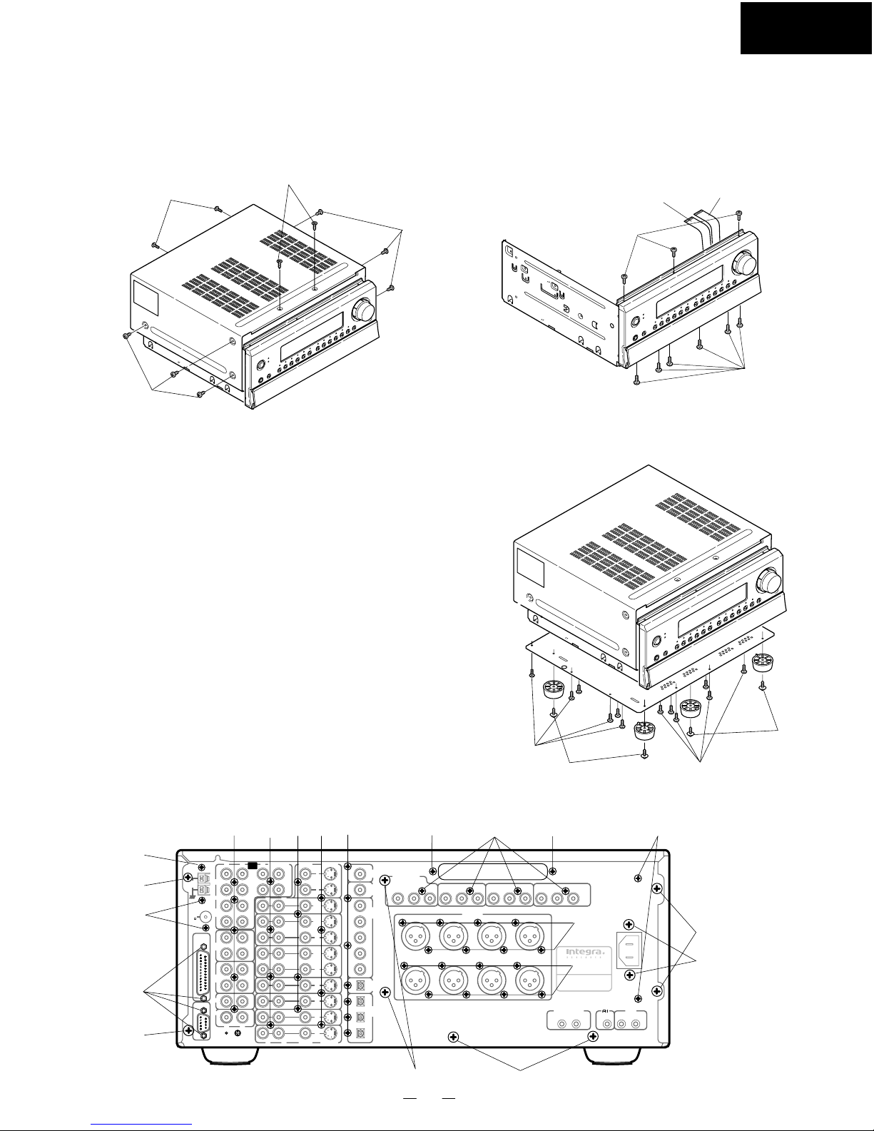
DISASSEMBLING PROCEDURES
Remove two screws A holding the top cover and bracket.
Remove six screws B holding the top cover and chassis.
Remove two screws C holding the top cover and the rear panel.
Lift up the top cover and remove it.
1. Top cover
2. Front panel assembly
Remove the top cover.
Disconnect two FFCs on the sockets of P7201B and P7202A.
Remove three screws D holding the front panel and chassis
from the top side.
Remove six screws E holding the front panel and chassis
from the bottom side.
3. Bottom board
Remove four screws F holding the leg and chassis.
Remove twelve screws G holding the bottom board and chassis.
4. Rear panel
When PC board assembly are removed, remove the rear panel.
Remove the 8 screws
A
holding the rear panel and the chassis.
Remove the four special screws C.
Remove the 46 screws D to K.
Remove the two screws N.
A
B
C
D
E
F
G
H
I
J
K
L
M
N
: ATTB+8C(BC) (Part No.838440089) x 8 Chassis
: 3TTB+6B(BC) (Part No.838440068) x 3 Tuner unit
: Special screw (This screw is included to Terminal)
x 4 Multi channel input PC board
: 3TTB+8B(BC) (Part No.838430088) x 5 Input selector PC board
: 3TTB+8B(BC) (Part No.838430088) x 4 Input/Output terminal PC board
: 3TTB+8B(BC) (Part No.838430088) x 4 Video terminal PC board
: 3TTB+8B(BC) (Part No.838430088) x 4 S Video terminal PC board
: 3TTB+8B(BC) (Part No.838430088) x 7 DSP circuit terminal PC board
: 3TTB+8B(BC) (Part No.838430088) x 8 XLR jack PC board (1)
: 3TTB+8B(BC) (Part No.838430088) x 8 XLR jack PC board (2)
: 3TTB+8B(BC) (Part No.838430088) x 2 Primary circuit PC board
: 3TTB+8B(BC) (Part No.838430088) x 4 Component video PC board
: 3TTB+8B(BC) (Part No.838430088) x 2 Cover
: 3TTB+8B(BC) (Part No.838430088) x 2 Primary circuit PC board
C
B
A
B
D
E
P7202
P7201
F
F
G
G
DVD
VIDEO
5
VIDEO
4
VIDEO
3
ZONE 2
MONITOR
OUT
VIDEO
1
VIDEO
2
R
L
R
L
C
SUBWOOFER
IR IN
MAIN ZONE 2
VIDEO
S VIDEO
VIDEO
S VIDEO
INPUT 2
P
BPR
Y
INPUT 3
PBP
R
Y
OUTPUT
PBP
R
Y
OUT
OUT
IN
IN
IN
IN
IN
IN
AC
INLET
OUT
1
2
FM
ANT.
75
AM
ANT.
C D
GND
MULTI
CHANNEL
INPUT
RS 232
TAPE
2
TAPE
1
FRONT
3
2
1
3
2
5
4
1
I N
I
N
I
N
I
N
OUT
OUT
L
R
L
1212121
2
R
COMPONENT
VIDEO
INPUT 1
P
BPR
Y
DIGITAL
OUTPUT
(
COAXIAL
)
AC-3
RF
DIGITAL
INPUT
(
COAXIAL
)
DIGITAL
OUTPUT
(
OPTICAL
)
DIGITAL
INPUT
(
OPTICAL
)
PHONO
SURR
BACK
SURR
PRE
OUT
RIGHT CENTER SUBWOOFER
SURROUND
RIGHT
SURROUND
LEFT
SURROUND BACK
RIGHT
SURROUND BACK
LEFT
LEFT
PRE OUT
AV CONTROLLER
MODEL NO.
RDC-7
12V TRIGGER
AB
N
EFGH
L
I
J
K
MM
A
A
A
A
C
A
B
B
D
Page 12
RDC-7
12
2
3
1
4
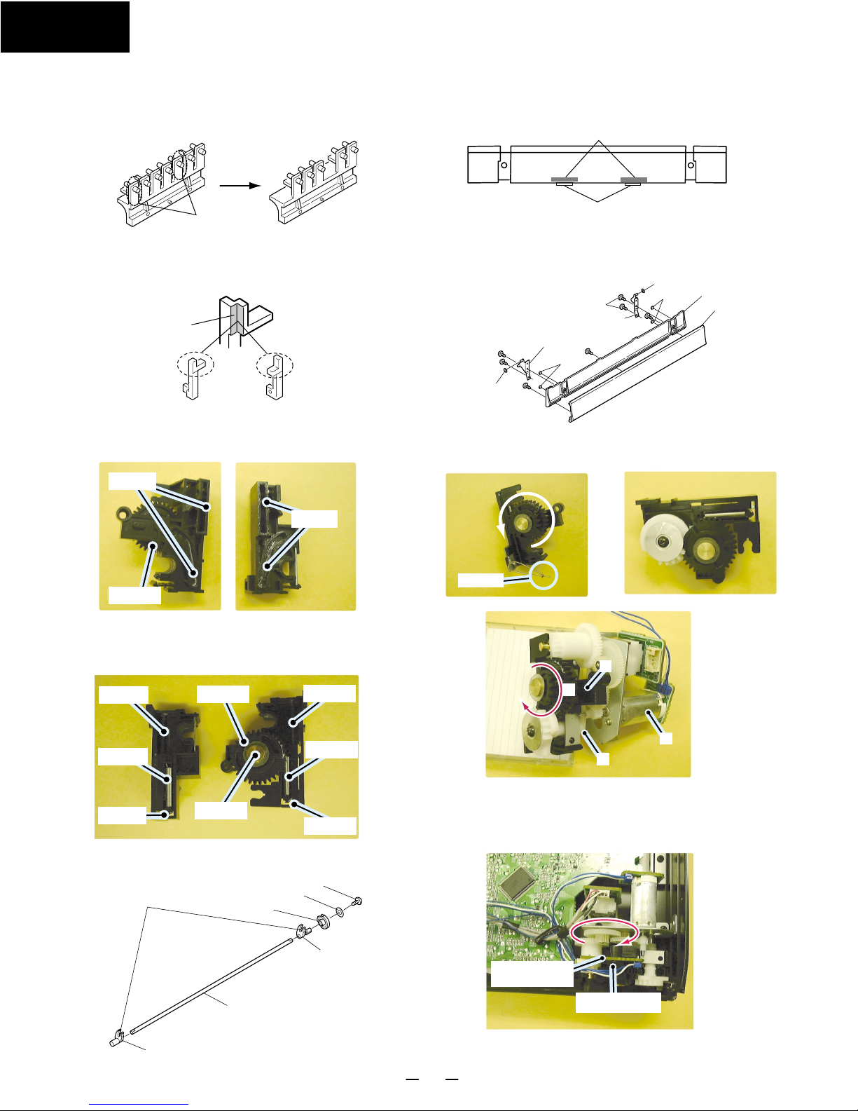
4. Attachment of shaft assembly
Apply Floil on the groove of holders.
Hang the spring from the down side of lever.
Attach the gear A to the holder R, and insert the
shaft A to fix the gear A.
Holder R Holder L
Gear A
Groove
Attach the gear S as shown
below.
Holder R
Spring
Lever
Shaft A
Gear A
Holder L
Spring
Lever
Insert the shaft to the shaft L and the shaft R.
Turn Gear A counter clockwise
fully.
Cross
1. Insert the retainer S.
2. Turn the gear A clockwise fully.
3. Insert the headphone jack to the front panel
4. Attach the motor assembly.
5. Attach the part above on the front panel.
Turn the gear clockwise fully and insert
the PC board ass'y (NAETC-6835)
Fix the PC board ass'y by the plastic rivet.
Plastic rivet
PC board ass'y
NAETC-6833
Groove
Shaft L
Shaft
Shaft R
Gear S
Retainer W
2.6TTS+6B(BC)
Apply floil
ASSEMBLING PROCEDURES
1. Attachment of door knob
When you replace the door knob assembly of lef side, cut the
two knobs below.
Cut
3. Attachment of door
Put the cushions according to the center of rib.
Inlay the door base to the door.
Put the five cushions on the door base.
Attach the stay L and stay R.
Put the spacers on the stay L and the stay R.
Cushion
Rib
3. Attachment of holders
Lever L
Lever R
Apply the floil G-902S (Part No.260447) on the lever
L and the lever R.
2
3
1
4
Cushion
Stay R
Spacer
Door
Door base
Cushion
Stay L
Spacer
53
53 : 2.6TTS+6B(BC)
Floil
Gear A
Groove
Holder R
Spring
Lever
Shaft A
Gear A
Holder L
Spring
Lever
Cross
Plastic rivet
PC board ass'y
NAETC-6833
Groove
Page 13
RDC-7
Pin No.
12, 25, 51
63, 75, 89
100
1, 11, 23, 38
49, 64, 77, 88
74
50
52
24
26
76
4
5
6
28
30
Pin Descriptions
Q8704 : XCS05XL-4VQ100C
20
Page 14
RDC-7
21
Pin No.
36
2, 27,
54, 79
21, 48,
73, 99
80
72
30
73
Pin Descriptions
Page 15
RDC-7
25
Pin Function
A
0
to A
17
Address Inputs
DQ
0
to DQ
7
Data Inputs/Outputs
CE
Chip Enable
OE
Output Enable
WE
Write Enable
RY/BY
Ready/Busy Output
RESET
Hardware Reset Pin/Temporary Sector
Unprotection
N.C. No Internal Connection
V
SS
Device Ground
V
CC
Device Power Supply
18
A0 to A17
WE
OE
CE
DQ 0 to DQ 7
8
RESET
RY/BY
VSS
VCC
WE
CE
A
0 to A17
OE
Erase Voltage
Generator
DQ 0 to DQ 7
State
Control
Command
Register
Program Voltage
Generator
Low V
CC Detector
Address
Latch
X-Decoder
Y-Decoder
Cell Matrix
Y-Gating
Chip Enable
Output Enable
Logic
Data Latch
Input/Output
Buffers
STB
STB
Timer for
Program/Erase
RESET
RY/BY
Buffer
RY/BY
DESCRIPTION
BLOCK DIAGRAM
Q728,Q768: MBM29LV002/004TC-910PTN (Flash memory)
Page 16

RDC-7
29
Q8701 : CC1536E (MASTER CLOCK MODULE)
3
1
1
2
L1
C15
.1uF
TP1
+16VIN
R11
1
C7
4.7uF
20%
16V
C6
0.047uF
16V
VCOREGEN
MIC5205BM5
U5
1
3
2
5
4
OUT
ADJ
IN
GND
EN
R20
464
1% 1/10W
R22
3.92k
1% 1/10W
C24
0.047uF
20% 16V
C21
4.7uF
20% 16V
+11VOUT
+5V VCO
R19
4.99k
1% 1/10W
C22
1.0uF
20V
C20
0.01uF
R21
4.99k
1% 1/10W
PHASEADJ
GNDA
R16
3.92k
1% 1/10W
4
3
5
1
2
OPA237
C13
0.022uF
C14
0.22uF
C16
.1uF
16V
+11VOUT
VCO CTL
GNDA
C25
5600pF
R17
2.21k
1%
C19
.1uF
16V
CR4
BBY42
16V
0.27uH
4
3
1
7
852
6
VREF
TANK
OUT
VEE1
VEE2
AGC
VCC2
VCC1
U3
MC121480
C18
.1uF
16V
C17
4.7uF
20% 16V
C11
.01uF
R9
22
1/8W
R18
100
1% 1/8W
Q3
BFT93
VCOOUT
C12
.01uF
GNDA
+5VD
R23
18
1/2W
C9
4.7uF
20% 16V
C10
.01uF
C8
.047uF
16V
R12
464
1% 1/10W
R14
1.37k
1% 1/10W
+5V VCO
U2
1
2
3
5
4
OUT
ADJ
IN
GND
EN
11VREGEN
CR3
BAV99LT1
1
3
2
CR3
BAV99LT1
1
3
2
R13
19.1k
1% 1/10W
Q1
BSS84ZXC
Q2
BSS138ZX
R15
100k
1%
C26
.1uF
16V
5050
UP-
R10
100k
1%
DOWN
NOT ON PC BOARD
+5VD
GNDD
P1:S
P1:T
P1:U
P1:V
P1:W
P1:X
P1:Y
P1:Z
P1:AA
P1:AB
P1:AC
P1:AD
P1:AE
P1:AF
P1:AG
P1:AH
P1:AI
P1:AK
CLOCKON
LOCKOK
FSXOUT
WC IN
WC INN
FS0
FS1
FS2
O/E
+16VIN
GNDA
+11VOUT
PROGTDO
PROTCK
PROGTMS
PROGTDI
19
20
21
22
23
24
25
26
27
28
29
30
31
32
33
34
35
36
11VREGEN
VCOREGEN
1FS
WDCLK
P1:R
P1:Q
256/384FSYP1:P
P1:O
P1:N
P1:M
P1:L
P1:K
P1:J
P1:I
P1:H
P1:G
P1:F
P1:E
P1:D
P1:C
P1:B
P1:A
128/192FSY
GNDD
256FSB
128FSB
64FS
32FS
P1:P
2FS
1FS
05FS
FS4
WC INV
VCO CTL
GNDA
PHASEADJ
+5V VCO
18
17
16
15
14
13
12
11
10
9
8
7
6
5
4
3
2
1
PHADJGND
MCLKx2
MCLK
BITCLKx4
BITCLKx2
BITCLK
BITCLK:2
WDCLK
WDCLK:2
BITCLK:2
KEY
+5V VCO
R6
1.3k 1/10W
R5
1.3k 1/10WR71.3k 1/10W
DOWN
UP-
5050
VCOOUT
44
43
42
41
40
39
38
37
36
35
34
I/O
I/O
I/O
VCC
INPUT/OE2(GCLK2)
INPUT/GCLRn
INPUT/OE1n
INPUT/GCLK1
GND
I/O
I/O
I/O
I/O
IVCC
I/O
I/O(TMS)
I/O
I/O
GND
I/O
I/O
I/O(TDI)
I/O
GND
I/O
I/O(TCK)
I/O
I/O
VCC
I/O
I/O
I/O(TDO)
I/O
I/O
I/O
I/O
I/O
GND
VCC
I/O
I/O
I/O
I/O
I/O
12
13
14
15
16
17
18
19
20
21
22
2324252627282930313233
1110987654321
EPM7064STC44-10
U1
+5VD
+5VD
+5VD
(1024/1536FSBUF)
(512/736FSBUF)
+5VD
C23
1uF
25V
16V
.047uF
C1
+5VD
+5VD
R1
1.3k 1/10W
R2
1.3k 1/10W
R3
1.3k 1/10W
R4
1.3k 1/10W
R8
220k 1/10W
PROGTCK
PROGTDO
PROGTMS
PROGTDI
All resistors are thick film or metal film.
All capacitor dilelectrics are X7R.
All capacitor values are in microfarads, 50V, 10%.
All resistor values are in ohms, 1/8W, 5%.
NOTE: Unless otherwise specified.
Page 17

31
32
RDC-7
RG RG RG RG RG
P7202A
P7201A
P7482A
P7451A
Red
Black
Red
Yellow
Paple
Yellow
Brown
White
Yellow
White
Blue
Gray
Blue
Brown
Brown
Orange
Green
Orange
NAAF-6814
P4711A
P3062B
P3061B
NAAF-6862
J4722B
NAAF-6861
J4723B
NAVD-6848
P2011
P2024
P2013
P2012
NAVD-6849
P2524
P2523
P2011
P2012
P2013
NAVD-6850
JL2711B
NAPS-6863
P9012
NADG-6860
P8006A
P9012A
P8005A
JL8002
JL9222B
JL9221B
NASW-6864
P9007C
NASW-6833
JL7601B
P7601B
NADIS-6832
P7451B
NAETC-6835
NAETC-6836
P7452B
P7452A
P2511A
JL2711A
P2011A
P2512AP2513A
P2013AP2012A
P9212AP9312A
P7201B
P7202A
NAAF-6813
P3011B
P3012B
P3013B
P3011B
P8005
P8006
J3015B
J4273A
J4722A
P4711B
NAAF-6815
P7921B
J3015A
NAPS-6838
NAPS-6839
P9211A
P9212
P9311A
P9312
J8002B
JL9221B
JL9222B
Q9202
D9201
Q9301
Q9304
Q9322
Q9303
D9301
P705
P704
P703
P702
P701
NADG-6830
NAAR-6837
P7002AP7001A
P7003A P7006A P7007A
P3002A
P3001A
P4002AP4003AP4004A P4001A
P1201A
P7921A
NAETC-6834
TUNER UNIT
P9011A
P9011A
T9001
POWER
TRANSFORMER
SUBWOOFER
1
2
ZONE 2
VIDEO1
VIDEO2
VIDEO 3
VIDEO 4
VIDEO 5
DVD
RIGHTLEFTCENTERSUBWOOFER
SURROUND
BACK
LEFT
SURROUND
BACK
RIGHT
SURROUND
LEFT
SURROUND
RIGHT
FRONT
SURROUND
SURROUND
BACK
TAPE 1
TAPE 2
CD
PHONO
MULTI
CHANNEL
INPUT
RS232C
AM ANT
FM ANT
POWER
ON/OFF
AC INLET
T9002
MONITOR
ZONE2
VIDEO
1
VIDEO5VIDEO
4
VIDEO3VIDEO
2
DVD
MONITOR
ZONE2
VIDEO
1
VIDEO5VIDEO4VIDEO3VIDEO
2
DVD
VIDEO
S VIDEO
AC-3
RF
DIGITAL
OUTPUT
DIGITAL
INPUT
(COAXIAL)
DIGITAL
INPUT
DIGITAL
OUTPUT
12V TRIGGER
AB
RIIR IN
MAIN
ZONE 2
PRE OUT
PRE OUT
COMPONENT VIDEO
INPUT 1INPUT 2INPUT 3OUTPUT
P772
P772A
Yellow
White
White
Brown
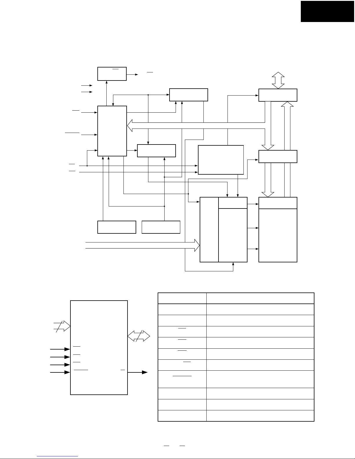
WIRING VIEW
INPUT/OUTPUT
SELECTOR PC BOARD
INPUT OUTPUT
TERMINAL PC BOARD
MULTI CHANNEL
INPUT TERMINAL
PC BOARD
DSP CIRCUIT PC BOARD
DISPLAY & SUB MICROPROCESSOR PC BOARD
CONTROL SWITCH
PC BOARD
HEADPHONE JACK
PC BOARD
DOOR MOTOR DRIVER
PC BOARD
DOOR MOTOR
PC BOARD
MAIN MICROPROCESSOR PC BOARD
CONSTANT
VOLTAGE
CIRCUIT
PC BOARD
RECTIFIER
CIRCUIT
PC BOARD
VIDEO CIRCUIT
PC BOARD
S VIDEO TERMINAL
PC BOARD
COMPONENT VIDEO
TERMINAL PC BOARD
D/A CONVERTER PC BOARD
XLR JACK PC BOARD(1)
XLR JACK PC BOARD(2)
PRIMARY CIRCUIT
PC BOARD
POWER SWITCH
PC BOARD
Phones
U10
U13
U16
U15
U2
U1
U18
U17
U3
U9
U8
U7
U6
U5
U19
U12
U11
U20
U4
U14
U22
Page 18

33
34
RDC-7
RDC-7
CHASSIS EXPLODED VIEW
The special screw (Ref.No.85) is included
in the socket assembly.
97
50
86
83
83
53
9
9
9
20
16
17
72
72
9
95
49
74
80
79
48
45
76
55
54
65
64
66
69
53
68
70
18
18
70
56
46
46
26
82
81
81
81
77
71
77
77
77
26
26
9
9
96
52
51
18
58
59
U8
63
62
61
60
56
U9
U7
U5
U11
U12
U3
U1
U2
U13
U14
U4
U15
U22
U10
U6
P7201
P7202
P1201
18
18
84
3
3
18
9
19
19
19
15
78
44
39
9
9
37
38
9
9
40
39
39
40
40
U7
19
18
43
42
41
44
44
42
T9001
4
4
1
2
6
6
5
5
9
9
9
38
9
14
14
8
8
10
88
90
90
87
90
91
9
11
13
12
12
9
91
9
9
21
21
22
P2525
22
92
98
85
27
19
9
9
9
9
19
110
P3005
P3005a
93
87
101
90
9
9
5
P3006
3
5
5
23
U18
U17
7
25
23
F9004
F9002
F9001
U19
P772
5
38
38
U16
9
3
47
47
57
18
72
67
53
9
53
102
103
104
44
Page 19

35
36
RDC-7
REF. NO.
1
2
3
4
5
6
7
8
9
10
11
12
13
14
15
16
17
18
19
20
21
22
23
25
26
27
37
38
39
40
41
42
43
44
46
47
48
49
50
51
52
53
54
55
56
57
58
59
60
61
62
63
64
65
66
67
68
69
70
71
72
PART NO.
27100319-2
28170070
27255004
27190813
29110083
28141421
28141423
27130778
838430088
27115259-1
27160462-1
838430107
27190009
27190902
27130779E
27190938
27300833
82143006
838440089
27130832-1A
27130837-1
28141095
27190369
27190470
82143010
838430068
27170309
838130088
27175317
831430088
27130780-1
28170071
260208
830440089
28198903
28141432
28125375
28125376
28148435
28183002A
28183003A
834426068
27191094A
28335065A
27180577
27191095A
27141758A
27180579
28335066A
27301943
27260364
880011
27260363
27260365A
27260366A
27270218
27301942
27141759
27141752
24804045B
28141426
DESCRIPTION
Chassis
Bushing
CS-1, Clip
KGPS-10RF, Holder
Adhesive tape 16u
t8*10*30, Cushion
t16*20*30, Cushion
Bracket P
3TTB+8B(BC), Self tapping screw
Side bracket
Heat sink S
3TTB+10S(BC), Self tapping screw
KGLS-4S, Holder
KGPS-16S, Holder
Bracket Shield
KGPS-8S, Holder
WS-2NS, Clamp
3P+6FN(BC), Pan head screw
4TTB+8C(BC), Self tapping screw
Bracket F
Bracket U
Cushion
Holder
KGLS-18S, Holder
3P+10FN(BC), Pan head screw
3TTB+6B(BC), Self tapping screw
Bottom board
TTB+8B(BC), Self tapping screw
Leg
3TTW+8B(BC), Self tapping screw
Bracket PT
Bushing
Wire tie
4TTC+8C(BC), Self tapping screw
Facet
t1.5*12*4, Cushion
End cap, SL
End cap, SR
Door base
Stay L
Stay R
2.6TTS+6B(BC), Self tapping screw
Holder L
Lever L
Spring
Holder R
Retainer SP
Spring, door
Lever R
Gear A
Shaft A
NRP-355, Plastic rivet
Shaft
Shaft L
Shaft R
Spacer
Gear
Retainer W
Retainer S
Motor
t1.5*25*5, Cushion
CHASSIS EXPLODED VIEW PARTS LIST
<UDD>
<UDT>
<UPT>
<UPP>
<UGT>
<UJJ>
NOTE:
120V model only
Asian model only for 120V
Asian model only for 230V
European model only
220V model only
Japanese model only
REF. NO.
73
74
76
77
78
79
80
81
82
83
84
86
87
88
90
91
92
93
95
96
97
98
101
102
103
104
110
F9001
F9002
F9004
P1201
P2525
P3005
P3005a
P3006
P7201
P7202
P772
P9001
T9001
PART NO.
28141430
28191883A
28325748
28325746
28325751
27268016A
27130838
28325723A
27141755
28140860
27190926
28325754
28184776A
28141422
838240089
801599
28184772
28141441
27212194
27212195
27262646
27262647
28148439
27122714C
27122715A
27122726A
27122716A
29362591
29360778
29362686
29095880
25055959
252163
252074
252164
2047152512
2047261022
25060151
87643010
27262657
2047242512
2047242512
2044110142
253301HIT
253302HIT
253303HIT
2301456A
2301457A
2301458A
2301455A
DESCRIPTION
Cushion
Clear plate
Knob AS(ST)
Knob AS(SEL)
Knob AS(POWER)
Guide (VOL AS)
Bracket, volume
Knob, door
Bracket, knob
Cushion
KGPS-18RF, Holder
Knob (VOL)AS
Top cover
t12x15x30, Cushion
4TTB+8C(NI), Self tapping screw
Special screw (HFC)
Cover
Cushion
Front panel <UDD,UDT,UPT,UGT,UJJ>
Front panel <UPP>
Plate L <UDD,UDT,UPT,UGT,UJJ>
Plate L <UPP>
Door
Rear panel <UDD,UDT>
Rear panel <UPP,UPT>
Rear panel <UGT>
Rear panel <UJJ>
Label
Label flash <UDD>
Label, door
0.515*900*900 Sheet,
NPLG-1P912 Shorted plug
4A-UL/T-237, Fuse <UDD, UDT>
2A-SE-EAK, Fuse <UPP,UPT, UGT>
5A-UL/T-237, Fuse <UJJ>
NCFC7-152512, Flexible flat cable
NCFC7-261022, Flexible flat cable
Ground terminal
W3*10F(BC), Flat washer
Shield plate
NCFC7-242512, Flexible flat cable
NCFC7-242512, Flexible flat cable
NCFC4-110142, Flexible flat cable
AS-UC-2, Power supply cord <UDD,UDT>
AS-CEE-3, Power supply cord <UPP,UGT,UPT>
AS-JA Power supply vord <UJJ>
NPT-1392D, Power transformer <UDD,UDT>
NPT-1392P, Power transformer <UPP,UPT>
NPT-1392G, Power transformer <UGT>
NPT-1392J, Power transformer <UJJ>
NOTE: THE COMPONENTS IDENTIFIED BY MARK ARE
CRITICAL FOR RISK OF FIRE AND ELECTRIC SHOCK.
REPLACE ONLY WITH PART NUMBER SPECIFIED.
REF. NO.
U1
U2
U3
U4
U5
U6
U7
U8
U9
U10
U11
U12
U13
U14
U15
U16
U17
U18
U19
U20
U22
PART NO.
1A871513-1F
1A871513-1G
1A871514-1F
1A871514-1G
1A871515-1F
1A871515-1G
1A871530-2
1A871532-1F
1A871532-1G
1A871532-1H
1A871532-1I
1A871533-1F
1A871533-1G
1A871533-1H
1A871533-1I
1A871534-1F
1A871534-1G
1A871534-1H
1A871534-1I
1A871535-1F
1A871535-1G
1A871535-1H
1A871535-1I
1A871536-1F
1A871536-1G
1A871536-1H
1A871536-1I
1A871537-1F
1A871537-1G
1A871537-1H
1A871538-1F
1A871538-1G
1A871538-1H
1A871539-1F
1A871539-1G
1A871539-1H
1A871548-1F
1A871548-1G
1A871549-1F
1A871549-1G
1A871550-1F
1A871550-1G
1A871560-2
1A871561-2F
1A871561-2G
1A871561-2H
1A871561-2I
1A871562-2F
1A871562-2G
1A871562-2H
1A871562-2I
1A871563-2F
1A871563-2G
1A871563-2H
1A871563-2I
1A871564-2F
1A871564-2G
1A871564-2H
1A871564-2I
240134
240135
240133
DESCRIPTION
NAAF-6813-1F, Input /output selector PC board ass'y board ass'y <UDD,UDT,UJJ>
NAAF-6813-1G, Input /output selector PC board ass'y board ass'y <UPP,UPT,UGT>
NAAF-6814-1F, Input /output terminal PC board ass'y board ass'y <UDD,UDT,UJJ>
NAAF-6814-1G, Input /output terminal PC board ass'y board ass'y <UPP,UPT,UGT>
NAAF-6815-1F, Multi channel input terminal PC board ass'y <UDD,UDT,UJJ>
NAAF-6815-1G, Multi channel input terminal PC board ass'y <UPP,UPT,UGT>
NADG-6830-2, DSP circuit PC board ass'y
NADIS-6832-1F, Display & Sub-microprocessor PC board ass'y <UDD>
NADIS-6832-1G, Display & Sub-microprocessor PC board ass'y <UPP>
NADIS-6832-1H, Display & Sub-microprocessor PC board ass'y <UPT,UDT,UGT>
NADIS-6832-1I, Display & Sub-microprocessor PC board ass'y <UJJ>
NASW-6833-1F, Operation switch PC board ass'y <UDD>
NASW-6833-1G, Operation switch PC board ass'y <UPP>
NASW-6833-1H, Operation switch PC board ass'y <UPT,UDT,UGT>
NASW-6833-1I, Operation switch PC board ass'y <UJJ>
NAETC-6834-1F, Headphone jack PC board ass'y <UDD>
NAETC-6834-1G, Headphone jack PC board ass'y <UPP>
NAETC-6834-1H, Headphone jack PC board ass'y <UPT,UDT,UGT>
NAETC-6834-1I, Headphone jack PC board ass'y <UJJ>
NAETC-6835-1F, Door motor drive PC board ass'y <UDD>
NAETC-6835-1G, Door motor drive PC board ass'y <UPP>
NAETC-6835-1H, Door motor drive PC board ass'y <UPT,UDT,UGT>
NAETC-6835-1I, Door motor drive PC board ass'y <UJJ>
NAETC-6836-1F, Door motor PC board ass'y <UDD>
NAETC-6836-1G, Door motor PC board ass'y <UPP>
NAETC-6836-1H, Door motor PC board ass'y <UPT,UDT,UGT>
NAETC-6836-1I, Door motor PC board ass'y <UJJ>
NAAR-6837-1F, Main microprocessor PC board ass'y <UDD>
NAAR-6837-1G, Main microprocessor PC board ass'y <UPP>
NAAR-6837-1H, Main microprocessor PC board ass'y <UPT,UDT,UGT,UJJ>
NAPS-6838-1F, Rectifier circuit PC board ass'y <UDD>
NAPS-6838-1G, Rectifier circuit PC board ass'y <UPP>
NAPS-6838-1H, Rectifier circuit PC board ass'y <UPT,UDT,UGT,UJJ>
NAPS-6839-1F, Constant voltage circuit PC board ass'y <UDD>
NAPS-6839-1G, Constant voltage circuit PC board ass'y <UPP>
NAPS-6839-1H, Constant voltage circuit PC board ass'y <UPT,UDT,UGT,UJJ>
NAVD-6848-1F, Video circuit PC board ass'y <UDD,UJJ>
NAVD-6848-1G, Video circuit PC board ass'y <UDT,UPP,UPT,UGT>
NAVD-6849-1F, S Video terminal PC board ass'y <UDD,UJJ>
NAVD-6849-1G, S Video terminal PC board ass'y <UDT,UPP,UPT,UGT>
NAVD-6850-1F, Component video terminal PC board ass'y <UDD,UJJ>
NAVD-6850-1G, Component video terminal PC board ass'y <UDT,UPP,UPT,UGT>
NADG-6860-2, D/A Converter circuit PC board ass'y
NAAF-6861-2F, XLR jack PC board ass'y (1) <UDD,UDT>
NAAF-6861-2G, XLR jack PC board ass'y (1) <UPP,UPT>
NAAF-6861-2H, XLR jack PC board ass'y (1) <UGT>
NAAF-6861-2I, XLR jack PC board ass'y (1) <UJJ>
NAAF-6862-2F, XLR jack PC board ass'y (2) <UDD,UDT>
NAAF-6862-2G, XLR jack PC board ass'y (2) <UPP,UPT>
NAAF-6862-2H, XLR jack PC board ass'y (2) <UGT>
NAAF-6862-2I, XLR jack PC board ass'y (2) <UJJ>
NAPS-6863-2F, Primary circuit PC board ass'y <UDD,UDT>
NAPS-6863-2G, Primary circuit PC board ass'y <UPP,UPT>
NAPS-6863-2H, Primary circuit PC board ass'y <UGT>
NAPS-6863-2I, Primary circuit PC board ass'y <UJJ>
NASW-6864-2F, Power switch PC board ass'y <UDD,UDT>
NASW-6864-2G, Power switch PC board ass'y <UPP,UPT>
NASW-6864-2H, Power switch PC board ass'y <UGT>
NASW-6864-2I, Power switch PC board ass'y <UJJ>
TFCE1U114A, Tuner unit <UDD>
TFCE1E512A, Tuner unit <UPP, UDT, UPT,UGT>
TFCE1J114A,Tuner unit <UJJ>
Page 20

37
38
RDC-7
RDC-7
123456789
101112131415161718192021222324252627282930
100
99
98
97
96
95
94
93
92
91
90
89
88
87
86
85
84
83
82
81
31
32
33
34
35
36
37
38
39
40
41
42
43
44
45
46
47
48
49
50
8079787776757473727170696867666564636261605958575655545352
51
TUNER UNIT
+5V
+5V
X7001
16MHz OSC
Q7002
SYSTEM
RESET
POWER
FAILURE
DET
AC IN
+5V
+5V
U1
U22
U5
U16
U16
U4
U16
U7 U1,U17,18
Q4214
TC9482F
Q4216
TC9482F
16 STB
15 DATA
14 CK
16 STB
15 DATA
14 CK
16 STB
15 DATA
14 CK
16 STB
15 DATA
14 CK
Q4210
TC9482F
Q4212
TC9482F
FRONT L/R
SURROUND L/R
SURROUND BACK L/R
CENTER/SUBWOOFER
Q1502
BU1923F
13
15
16
13
15
16
Q4010
TC9163AF
Q4020
TC9163AF
Q3220
TC9274AF-008
Q3030
TC9163AF
Q3040
TC9164AF
INPUT SELECTOR
(VIDEO/DVD)
INPUT SELECTOR
(TAPE)
INPUT SELECTOR
(PHONO,CD)
23 FUNC
21 CL
22 DATA
13 STB
15 CL
16 DATA
13 STB
15 CL
16 DATA
20 CS
23 CLK
22 DI
20 CS
23 CLK
22 DI
Q4320
NJU7306G
Q4326
NJU7306G
TONE CONTROL
(FRONT L/R)
TONE CONTROL
(CENTER/SUBWOOFER))
Q9501
Q9502
RL9001
FDATA
FCLK
CFSTB
TDATA
TCLK
~TCS1
~TCS2
VSS
VSS
VPDATA
VPCLK
~RESET
XOUT
VSS
XIN
VCC
VSTB
~RDSSCK
~POFF
PLLCE
RDSDATA
RDSSIG
~STEREO
~SD
DIGSO
DIGSI
DIGSCK
~INTRQ1
~INTRQ2
2NDPLLCS
2NDPLLLOCK
~AD/DIR
~SUBREQ
MAINSO
SUBSO
MAINSCK
~MAINREQ
XSTATE
ERROR
CSFLAG
~RFDIRRST
RFSYNC
~DARST
~ADRST
DFS
APGLOCK
F0
IPSTB
VCC
VREF
SUBRESET
VSS
RES1
RES2
SUBPOFF
RES4
9k/10k
ADR2915
MPOWER
DIGCS
AUTO
AUDIO
~CSSRAM
~CSFLASH
IEEEMOD1CLK
DSPMOD
IEEEMOD2
IEEEMOD1
~DSPRST1
~DSPRST2
~DACCS
~DIRCS
2NDPLLCLK
~DSPCS1
~DSPCS2
ADR3016
ADR3015
ADR3017
ADR2918
ADR2917
ADR2916
VSS
PRTCTV
VCC
~PRTCTTHM
~TRG12B
~TRG12A
POWERL
SPRL
AMUT
HPMUT
MRMUT
TUMUT
F2
F1
Q721
CS493002
DSP
Q761
CS493002
DSP
Q701
LC89055W
Q7001
M30624FGFP
MAIN MICROPROCESSOR
T9001
POWER
TRANSFORMER
12V
TRIGGER
A
B
Q3410-Q3413
ZONE MUTE
SWITCH
Q4803-Q4806
HEADPHONE
MUTE SW
AUDIO
MUTING
SWITCH
(POST PROCESSING)
3836353780
122423
Q7201 M30624F
#34 SUBREQ
#35 MAINSO
#36 MAINSI
#37 MAINSCK
#38 MAINREQ
79
78
#97 SUBRESET
#95 RES1
#94 RES2
#93 SUBOFF
#92 RES4
FRONT L
FRONT R
Q8001
PCM1704
Q8032
PCM1704
Q8031
PCM1704
Q8002
PCM1704
Q8101
AD1853JRS
Q8101
AD1853JRS
Q8101
AD1853JRS
Q8701
CC1536
22 LOCKOK
Q8776
TC9246F
REF 1
CKO 10
15 LOCK
Q8702
74HCT7007
Q8705
SM5847AF
1 DATA
2 BCLK
7 WCLK
1 DATA
2 BCLK
7 WCLK
1 DATA
2 BCLK
7 WCLK
1 DATA
2 BCLK
7 WCLK
2 MCLK
24 RST
25 L/R CLK
26 BCLK
27 SDATA
2 MCLK
24 RST
25 L/R CLK
26 BCLK
27 SDATA
2 MCLK
24 RST
25 L/R CLK
26 BCLK
27 SDATA
I/09 9
Q8704
XCS05XL
LA O 61
LA O 65
LRCLKO 62
LBO 56
RAO 57
RBO 55
LRCLKOUT 8
SCLOCKO 7
DBOUT 40
DC OUT 42
DD OUT 44
78 F0
71 F1
68 F2
#50 F0
#51 F1
#52 F2
Q8776
TC9246F
2ND PLL
MI 11
LOCK 15
Q7702
QUAD 4-CH
MULTIPLEXER
A 14
XSTATE 17
ERROR 34
CSFLAG 25
QUAL 1
RDATA 2
CLK 16
Q131
PM4007A
RESET 3
MUTO 66
Q103
AK5394VS
RESET 10
CMODE 18
SCD IN 6
SCCLK 7
SCDIO/SCDOUT 19
ABOOT/INTREQ 20
CS 18
SCD IN 6
SCCLK 7
SCDIO/SCDOUT 19
ABOOT/INTREQ 20
CS 18
Q821
TC74VHC245
OCTAL BUS
TRANSCEIVER
Q822
TC74VHC245
#28 DIGSCK
#26 DIGSO
Q823
TC74HCT7007
HEX BUFFER
#48 DFS
#47 ADRST
#43 RFDIRRST
#44 RFSYNC
#27 DIG SI
DO 35
DI 36
#26 DIGSO
APGLOCK
APOGEE MASTER
CLOCK MODULE
SURROUND L
SURROUND R
SURROUND
BACK L
SURROUND
BACK R
CENTER
SUBWOOFER
#31 2ND PLL CS
#32 2ND PLL LOCK
Q174 74HC595F
8-BIT SHIFT
REGISTER/LATCH
Q172 74HC151F
Q173 74HC151F
#82 CSFLASH
#83 CSRAM
#29 INTREQ1
#30 INTREQ2
Q727
MPD442000
STATIC RAM
Q728
FLASH
MEMORY
Q767
MD442000
STATIC RAM
Q768
FLASH
MEMORY
Q7701
#88 ADR2918
#81 IEEE MODCLK
+5V
Q7721
TC74ACT153F
Q7723
TC74ACT153F
Q7722
TC74ACT153F
#73 2ND PLL CLK
S2 14
#71 DSPCS2
#72 DSPCS1
#77 DSPRST2
#76 DSPRST1
RESET 36
RESET 36
#78 IEEE MODE1
AUDIO 24
AUTO 32
#86 DIGCS
TC74HCT125FT
4-CHANNEL
MULTIPLEXER
4-CHANNEL
MULTIPLEXER
#85 AUTO
#84 AUDIO
OCTAL BUS
TRANSCEIVER
ELECTRONIC VOLUME
ELECTRONIC VOLUME
ELECTRONIC VOLUME
ELECTRONIC VOLUME
RDS DECODER
AUDIO SELECTOR
AUDIO SELECTOR
POWER
SWITCH
RELAY
SUB MICROPROCESSOR
INITIALIZING
D/A CONVERTER
D/A CONVERTER
D/A CONVERTER
D/A CONVERTER
D/A CONVERTER
D/A CONVERTER
D/A CONVERTER
DIGITAL FILTER
DIR
(Digital interface
receiver)
AC3 RF
DEMODULATOR
A/D CONVERTER
2ND PLL
MAIN MICROPROCESSOR CONNECTION DIAGRAM
Page 21

39
1
2
3
4
5
6
7
8
9
10
11
12
13
14
15
16
18
19
20
21
22
23
24
25
26
27
28
29
30
31
32
33
34
35
36
37
38
39
40
41
42
43
44
45
46
47
48
49
50
FDATA
FCLK
CFSTB
TDATA
TCLK
~TCS1
~TCS2
VSS
VSS
VPDATA
VPCLK
~RESET
XOUT
VSS
XIN
VCC
VSTB
~RDSSCK
~POFF
PLLCE
RDSDATA
RDSSIG
~STEREO
~SD
DIGSO
DIGSI
DIGSCK
~INTRQ1
~INTRQ2
2NDPLLCS
2NDPLLLOCK
~AD/DIR
~SUBREQ
MAINSO
MAINSI
MAINSCK
~MAINREQ
XSTATE
ERROR
CSFLAG
~RFDIRRST
RFSYNC
~DARST
~ADRST
DFS
APGLOCK
F0
O
O
O
O
O
O
O
I
I
O
O
I
O
I
I
I
O
I
I
O
I
I
I
I
O
I
O
I
I
O
I
O
I
O
I
O
O
I
I
I
O
I
O
O
O
I
O
H
CLK
H
H
CLK
L
L
H
CLK
H
CLK
L
H
H
H
L
L
H
H
CLK
L
L
H
H
H
L
H
H
CLK
L
H
H
H
L
H
L
L
H
H
H
Serial data output terminal of function switch for input and configuration.
Serial clock output terminal of function switch for input and configuration.
Serial clock output terminal of function switch for configuration.
Serial data output terminal of tone control IC.
Serial clock output terminal of tone control IC.
Chip select output terminal of tone control IC for front channel.
Serial data output terminal of tone control IC for center and sub woofer.
Input terminal to switch the bus width of external data. Connect to the ground.
Input terminal to switch processor mode. Connect to the ground.
Serial data output terminal of electrical volume and PLL ICs.
Serial clock output terminal of electrical volume and PLL ICs.
System reset input terminal.
Oscillator circuit output terminal of main clock.
Power supply terminal. Connect to the ground.
Oscillator circuit input terminal of main clock.
Power supply terminal. Connect to +5V.
Strobe output terminal of electrical volume.
Clock input terminal from RDS modulator IC.
Input terminal for power failure detection.
Strobe output terminal of PLL IC.
DATA input terminal from RDS modulator IC.
Signal strength detection terminal of tuner.
FM stereo broadcast detection terminal.
Signal strength detection terminal of tuner.
Serial data output terminal to DSP ICs.
Serial data input terminal from DSP and DIR ICs.
Serial clock output terminal to DSP ICs.
INTRQ input terminal from DSP2.
INTRQ input terminal from DSP1.
Serial chip select output terminal of second PLL IC.
Lock detection input terminal from second PLL IC
ADC/DIR select output terminal
Request input terminal from sub microprocessor
Serial data output terminal of sub microprocessor
Serial data input terminal from sub microprocessor
Serial clock output terminal of sub microprocessor
Request output terminal from sub microprocessor
Source clock change monitor input terminal (DIR)
Flag input terminal for PLL lock error or data error.
Port of flash memory rewriting (DIR)
Update flag input terminal of head 40 bits of channel status
DIR/AC-3 RF RESET output terminal (common)
Synchronizing input terminal for AC-3 RF
Reset signal output terminal for DAC
Port of flash memory rewriting (DIR)
Reset signal output terminal for ADC
Sampling frequency control output terminal for ADC/DAC
Lock ok signal detection terminal of apgee master clock unit.
Sampling frequency control output terminal for Gate array (Q8704)
No. Function I/O Act. Description
MAIN MICROPROCESSOR TERMINAL DESCRIPTION
Q7001 : M30624FGFP
Page 22

40
RDC-7
51
52
53
54
55
56
57
58
59
60
61
62
63
64
65
66
67
68
69
70
71
72
73
74
75
76
77
78
79
80
81
82
83
84
85
86
87
88
91
92
93
94
95
96
97
98
99
100
F1
F2
TUMUT
MRMUT
HPMUT
AMUT
SPRL
POWERL
~TRG12A
~TRG12B
~PRTCTTHM
VCC
PRTCTV
VSS
ADR2916
ADR2917
ADR2918
ADR3017
ADR3015
ADR3016
~DSPCS2
~DSPCS1
2NDPLLCLK
~DIRCS
~DACCS
~DSPRST2
~DSPRST1
IEEEMOD1
IEEEMOD2
DSPMOD
IEEEMOD1CLK
~CSFLASH
~CSSRAM
~AUDIO
AUTO
DIGCS
MPOWER
ADR2915
9k/~10k
MSPORT4
~SUBPOFF
MSPORT2
MSPORT1
VSS
~SUBRESET
VREF
VCC
IPSTB
O
O
O
O
O
O
O
O
O
O
I
I
I
I
O
O
O
O
O
O
O
O
O
O
O
O
O
O
O
O
O
O
O
I
I
O
O
O
I
O
O
O
O
I
O
I
I
O
H
H
H
H
H
H
H
H
L
L
L
H
H
H
H
H
H
H
L
L
CLK
L
L
L
L
H
H
H
H
L
L
L
H
H
L
H
H
H
L
H
H
L
H
Sampling frequency control output terminal for Gate array (Q8704)
Sampling frequency control output terminal for Gate array (Q8704)
Muting control output terminal for tuner section.
Muting control output terminal for zone 2.
Muting control output terminal for headphone.
Muting control output terminal for analog section.
Speaker relay control output terminal.
Power relay control output terminal.
12V trigger output terminal.
12v trigger output terminal.
Thermal protection detection input terminal
Power supply terminal. +5V.
Current/Voltage detection input terminal of protection circuit
Power supply terminal. Connect to the ground.
Control output terminal for address 16 of flash memory IC Q728
Control output terminal for address 17 of flash memory IC Q728
Control output terminal for address 18 of flash memory IC Q728
Control output terminal for address 17 of flash memory IC Q768
Control output terminal for address 15 of flash memory IC Q768
Control output terminal for address 16 of flash memory IC Q768
Chip select output terminal to DSP IC 2
Chip select output terminal to DSP IC 1
Serial clock output terminal to second PLL IC
Chip select output terminal to DIR IC
Chip select output terminal to DAC
Reset output terminal to DSP IC 2
Reset output terminal to DSP IC 1
IEEE mode select output terminal. High level when clock of two lines and data of a line.
IEEE mode select output terminal. High level when clock of two lines and data of four lines.
High level when DSP 1.
Select output terminal of clock master or slave.
Chip select output terminal of flash memory ICs.
Chip select output terminal of SRAM ICs
Audio detect input terminal of DIR IC
Auto detect input terminal of DIR IC
Chip select output terminal of digital input switch
Initializing of power amplifier.
Address 15 control output terminal of flash memory
Initializing input terminal for band step of AM
Not used.
Signal control output terminal for power off of sub microprocessor
Not used.
Not used.
Power supply terminal for AD converter
Reset control terminal for sub microprocessor
Reference voltage input terminal for A/D converter
Power supply terminal for A/D converter. Connect to 5V.
Strobe output terminal for function switch
No. Function I/O Act. Description
Page 23

41
42
RDC-7
RDC-7
123456789
101112131415161718192021222324252627282930
0
VCC
VREF
KEY0
VSS
KEY1
KEY2
KEY3
SEL_NTSC
SEL_12V
SEL_AMP
SEL_RDS
DOOR_CL
DOOR_OP
FLRST
PWR_LED
ISVDET
RZSVDET
SYNCDET
HPIN
100
99
98
97
96
95
94
93
92
91
90
89
88
87
86
85
84
83
82
81
31
32
33
34
35
36
37
38
39
40
41
42
43
44
45
46
47
48
49
50
FLS0/OSDSO
FLSCK/OSDSCK
FLCS2
FLCS1
OSDCS
~REMIN
~ZRIN
VSS
VSS
VDSO
VDCLK
~RESET
XOUT
VSS
XIN
VCC
NMI
VOLENC2
VOLENC1
VSYNC
MOT_OP
MOT_CL
RESERVE2
RESERVE1
~SYSOUT
~R232RTS
~R232CTS
0
R232RX
R232TX
1394DOUT
I1394DIN
I1394CLK
1394CS
SUBSO
SUBSI
SUBCLK
~SUBREQ
LED_RED
LED_GREEN
~EPM
VD5_RZLED
VD4_RZLED
VD3_RZLED
VD2_RZLED
~CE
VD1_RZLED
DVD_RZLED
CD_RZLED
TP2_RZLED
8079787776757473727170696867666564636261605958575655545352
51
~MAINREQ
~TEIDEN
RESERVE4
AREA2
AREA1
SYSIN
00PHO_SLED
AM_SLED
FM_SLED
TP1_SLED
TP2_SLED
CD_SLED
DVD_SLED
VD1_SLED
VSS
VDST
VCC
VD2_SLED
VD3_SLED
VD4_SLED
VD5_SLED
0
STBY/RECV
0
PHO_RZLED
AM_RZLED
FM_RZLED
TP1_RZLED
Q7202
SYSTEM
RESET
Q7401
FL TUBE
30-BT-03G
Q7402
FL TUBE DRIVER
M66004FP
Q7403
FL TUBE DRIVER
M66004FP
Segment
Digit
Segment
Digit
X7201
16MHz
OSC.
U7201
REMOTE
CONTROL
SENSOR
M
Q7202
BUFFER
Q7451
DOOR MOTOR
DRIVER TA7291S
Q7533,Q7535
GATE CIRCUIT
Q7534,Q7536
GATE CIRCUIT
Q7461,Q7462
DOOR OPEN/
CLOSE DETECTOR
Q7571,Q7572
GATE CIRCUIT
Q2201
ON-SCREEN
DISPLAY CONTROL
LC74761-9189
Q2951
VIDEO
SELECTOR
SW TC9163AF
Q2952
VIDEO
SELECTOR
SW TC9164AF
+5V
+5V
Q2901
VIDEO CONTROL
SWITCH
TC9162AF
Q7001
MAIN MICROPROCESSOR
Q2181,Q2182
S VIDEO
DETECTOR
CIRCUIT
Q2191,Q2192
S VIDEO
DETECTOR
CIRCUIT
INPUT
RECORDING
P7481
HEADPHONE
SWITCH
S7461
MASTER
VOLUME
Phono AM FM Tape 1 Tape 2 CD
WAVEFORM
SHAPRER
WAVEFORM
SHAPRER
RI
INPUT/OUTPUT
IR INPUT
MAIN
IR INPUT
ZONE2
Standby Exit RIGHT LEFT Enter DOWN UP Menu
Open/Close CD PHONO FM AM Tape 2 Tape 1 Memory
FM Mode Preset > Preset< Video 5 Video 4 Video 3 VIideo 2 Vodeo 1 DVD
Tuning > Tinning < PTY/TP DSP > DSP < Zone2 Off Rec Out Display
D7516
POWER ON
+5V
+5V
INITIALIZING
INITIALIZING
Q7001
MAIN
MICROPROCESSOR
DVD Video 1 Video 2 Video 3 Video 4 Video 5
Standby
+5V
Phono AM FM Tape 1 Tape 2 CD
DVD Video 1 Video 2 Video 3 Video 4 Video 5
P7901
RS-232C
Q7901
BUFFER
+5V
SUB MICROPROCESSOR
CONNECTION DIAGRAM
Q7201
SUB MICROPROCESSOR
M30624F
+5V
Q7203
U10
U13
U16
U8
U3
Zone2/Rec Out INDICATOR
INPUT SOURCE INDICATOR
INPUT SOURCE INDICATOR
U13
U10
U7
Page 24

43
1
2
3
4
5
6
7
8
9
10
11
12
13
14
15
16
17
18
19
20
21
22
23
24
25
26
27
28
29
30
31
32
33
34
35
36
37
38
39
40
41
42
43
44
45
46
47
48
49
50
FLS0/OSDSO
FLSCK/OSDSCK
FLCS2
FLCS1
OSDCS
~REMIN
~ZRIN
VSS
VSS
VDSO
VDCLK
~RESET
XOUT
VSS
XIN
VCC
NMI
VOLENC2
VOLENC1
VSYNC
MOT_OP
MOT_CL
RESERVE2
RESERVE1
~SYSOUT
~R232RTS
~R232CTS
R232RX
R232TX
I1394DOUT
I1394DIN
I1394CLK
SUBSO
SUBSI
SUBCLK
~SUBREQ
LED_RED
LED_GREEN
~EPM
VD5_RZLED
VD4_RZLED
VD3_RZLED
VD2_RZLED
~CE
VD1_RZLED
DVD_RZLED
CD_RZLED
TP2_RZLED
O
O
O
O
O
I
I
O
O
I
I
I
I
O
O
O
O
O
O
I
O
I
O
O
I
O
O
O
I
O
O
O
O
O
O
O
O
O
O
O
O
O
O
H
CLK
H
H
H
L
L
H
CLK
H
H
H
H
H
H
H
H
L
L
L
0
H
H
H
H
CLK
0
L
L
CLK
L
H
H
L
H
H
H
H
L
H
H
H
H
Serial data output terminal for FL tube driver and on-screen ICs.
Serial clock output terminal for FL tube driver and on-screen ICs.
Chip selection output for FL tube driver IC 2.
Chip selection output for FL tube driver IC 1.
Chip selection output for on-screen IC.
Signal input terminal from remote control
Signal input terminal from remote control for zone 2
Switch input terminal for external data bus. Connect to ground terminal.
Switch input terminal for processor mode. Connect to ground terminal.
Serial data output terminal for video function switch IC.
Serial clock output terminal for video function switch IC.
Reset input terminal of microprocessor
Oscillator output terminal of main clock.
Power supply terminal. Connect to ground terminal.
Oscillator input terminal of main clock.
Power supply terminal. Connect to +5V.
Connect to 5V.
Input B terminal from rotary encoder for main volume.
Input A terminal from rotary encoder for main volume.
Video vertical synchronizing signal input terminal to judge synchronizing
Control output terminal to open the door.
Control output terminal to close the door.
Transfer request output terminal for main microprocessor.
Transfer request output terminal for main microprocessor.
RI code output terminal
Transfer request output terminal for RS232C.
Transfer data output terminal for RS232C.
Not used.
Receiving input terminal for RS232C
Transfer output terminal for RS232C.
Serial data output terminal for main microprocessor.
Serial data input terminal for main microprocessor.
Serial clock output terminal for main microprocessor.
Not used.
Serial data output terminal to main microprocessor.
Serial data input terminal from main microprocessor.
Serial clock input terminal from main microprocessor
Request signal output terminal to main microprocessor.
Output terminal to light up the red LED.
Output terminal to light up green LED.
EPM input terminal to write program.
Control output terminal for Video 5 recording or Zone 2 LED.
Control output terminal for Video 4 recording or Zone 2 LED.
Control output terminal for Video 3 recording or Zone 2 LED.
Control output terminal for Video 2 recording or Zone 2 LED.
Chip enable input terminal to write program.
Control output terminal for Video 1 recording or Zone 2 LED.
Control output terminal for DVD recording or Zone 2 LED.
Control output terminal for CD recording or Zone 2 LED.
Control output terminal for Tape 2 recording or Zone 2 LED.
No. Function I/O Act. Description
SUB MICROPROCESSOR TERMINAL DESCRIPTION
Q7201 : M30624FGFP
Page 25

44
RDC-7
51
52
53
54
55
56
57
58
59
60
61
62
63
64
65
66
67
68
69
70
71
72
73
74
75
76
77
78
79
80
81
82
83
84
85
86
87
88
89
90
91
92
93
94
95
96
97
98
99
100
TP1_RZLED
FM_RZLED
AM_RZLED
PHO_RZLED
STBY/RECV
VD5_SLED
VD4_SLED
VD3_SLED
VD2_SLED
VCC
VDST
VSS
VD1_SLED
DVD_SLED
CD_SLED
TP2_SLED
TP1_SLED
FM_SLED
AM_SLED
PHO_SLED
SYSIN
AREA1
AREA2
RESERVE4
~TEIDEN
~MAINREQ
HPIN
SYNCDET
RZSVDET
ISVDET
PWR_LED
FLRST
DOOR_OP
DOOR_CL
SEL_RDS
SEL_AMP
SEL_12V
SEL_NTSC
KEY3
KEY2
KEY1
VSS
KEY0
VREF
VCC
O
O
O
O
O
O
O
O
O
O
O
O
O
O
O
O
O
O
O
O
O
O
I
I
I
I
I
I
I
I
I
I
O
O
I
I
I
I
I
I
I
I
I
I
O
H
H
H
H
0
L
0
H
H
H
H
H
H
H
H
H
H
H
H
H
H
H
H
H
L
L
H
H
H
H
H
L
L
L
H
H
H
H
0
Control output terminal for Tape 1 recording or Zone 2 LED.
Control output terminal for FM recording or Zone 2 LED.
Control output terminal for AM recording or Zone 2 LED.
Control output terminal for Phono recording or Zone 2 LED.
Not used.
Control output terminal for Standby/Received indicator.
Not used.
Control output pin for Video 5 indicator.
Control output terminal for Video 4 indicator.
Control output terminal for Video 3 indicator.
Control output terminal for Video 2 indicator.
Power supply terminal. Connect to 5V.
Chip selection output terminal for video function switch.
Ground terminal.
Control output terminal for Video 1 indicator.
Control output terminal for DVD indicator.
Control output terminal for CD indicator.
Control output terminal for Tape 2 indicator.
Control output terminal for Tape 1 indicator.
Control output terminal for Video -1 indicator.
Control output terminal for Video -1 indicator.
Control output terminal for Video -1 indicator.
Not used.
Not used.
Input terminal for RI code.
Initializing input terminal 1 for tuner band
Initializing input terminal 2 for tuner band
Transfer request input terminal for main microprocessor.
Detection input terminal of power failure from main microprocessor.
transfer request input terminal for main microprocessor.
It is impression KEY input terminal (A/D input of 0) as for 0V.
External synchronizing signal input terminal for On-screen IC.
S video signal detection input terminal for recording signal.
S video signal detection input terminal for input signal.
Control output terminal for Power LED.
Reset terminal for FL tube driver IC
Detection input terminal to open the door.
Detection input terminal to close the door.
Initializing input terminal for RDS broadcast
Initializing input terminal for main amplifier
Initializing input terminal for 12V trigger
Initializing input terminal for NTSC.
Operation key 1 connection input terminal
Operation key 2 connection input terminal
Operation key 3 connection input terminal
Power supply terminal for AD converter. Connect to ground terminal.
Operation key 0 connection input terminal
Reference voltage input terminal for AD converter.
Power supply terminal for AD converter.
Not used.
No. Function I/O Act. Description
Page 26

45
46
RDC-7
RDC-7
1
2
3
4
5
ABCDEFG
H
MCL
GND
MCL
MCR
MCSW
GND
MCSL
MCSR
MCSBL
GND
MCSBR
+5S
GND
232RX
232RTS
232TX
232CTS
GND
LBP
AGND
RBP
-15V
MUTA
+15V
CBP
AGND
SWBP
MCL
AGND
MCC
MCR
MCSW
+15V
-15V
MCSL
MCSR
MCSBL
AGND
MCSBR
+5V
232CGND
232RX
232RTS
232TX
232CTS
GND
RI
RES4
RES3
MAINREQ
SYNCDET
RZSS
ISS
OSDCS
REMIN
Z2RIN
VDDA
VDCL
SUBRES
VSYNC
RES2
RES1
OUT1
OUT2
GND
OUT1
OUT2
GND
SLBP
AGND
SRBP
-15V
MUTA
+15V
SBLBP
AGND
SBRBP
SLBP
AGND
SRBP
-15V
MUTA
+15V
SBLBP
AGND
SBRBP
LBP
AGND
RBP
-15V
MUTA
+15V
CBP
AGND
SWBP
PLLSTB
VPDATA
VPCLNCGND
+5VTU
+12VTU
RDS
TUL
TUGND
TUR
TU MUTSDSTEREO
PLLSTB
VPDATA
VPCLNCGND
+5VTU
+12VTU
RDS
TUL
TUGND
TUR
TU MUTSDSTEREO
TUNER R
TUNER L
AGND
RZ2R
RZ2L
AGND
IL
AGND
IR
AGND
TUR
TUL
AGND
RZ2R
RZ2L
AGND
IL
AGND
IR
AGND
FAC2
FAC1
-VP
+5V
GND
GND
GND
+22V
+5.6S
FLOSDDA
FLOSDCL
1394DI
1394DO
1394CL
232CTS
232TX
232RX
232RTS
1394CS
+5V
CNVSS
HPR
HPE
HPL
FAC2
FAC1
-VP
+5V
GND
GND
GND
+22V
+5.6S
FLOSDDA
FLOSDCL
1394DI
1394DO
1394CL
232CTS
232TX
232RX
232RTS
1394CS
+5V
CNVSS
HPR
HPE
HPL
RI
RES4
RES3
MAINREQ
SYNCDET
RZSS
ISS
OSDCS
REMIN
Z2RIN
VDDA
VDCL
SUBRES
VSYNC
RES2
RES1
-15V
-15V
15S GND
15S GND
15S GND
SC GND
SC GND
SC GND
SC GND
+22V
+22V
+22V
-VPAC
FAC2
FAC1
12VDSP
5VDSP
5VDSP
-5VDSP
DSP GND
DSP GND
DSP GND
DSP GND
5V DAC
5V DAC
5S GND
5S GND
5S GND
-5V
-5V
AMUT
ISTB
FCL
FDATA
RBP
LBP
TDATA
TCL
T1STB
T2STB
VSTB
VPDATA
VPCL
+15V
15VGND
-15V
CFSTB
DL
AGND
DR
AGND
DLS
AGND
DRS
AGND
DSBL
AGND
DSBR
DC
DSW
DL
AGND
DR
AGND
DLS
AGND
DRS
AGND
DSBL
AGND
DSBR
DC
DSW
MUTZ2
FCL
ISTB
FDATA
-15V
GND
+15V
RZ2R
RZ2L
AGND
IL
AGND
IR
AGND
RZ2R
RZ2L
AGND
IL
AGND
IR
AGND
Z2MUT
FCL
ISTB
FDATA
-15V
15VGND
+15V
CA
CB
COFF
VGND
+5V
-5V
CA
CB
COFF
VGND
+5V
-5V
VCS
VDATA
VCK
+15V
15VGND
-15V
GND
SYNCVDOSDCS
OSDDA
OSDCL
DGND
+15V
DGND
RZSS
ISS
GND
VAR
VBR
VCR
-5V
GND
+5V
VCI
VBI
VAI
SYNCVDOSDCS
OSDDA
OSDCL
DGND
+15V
DGND
RZSS
ISS
VCS
VDATA
VCK
+15V
15VGND
-15V
GND
GND
VCR
VBR
VAR
-5V
GND
+5V
VCI
VBI
VAI
VGND
VAR
VBR
VCR
-5V
VGND
+5V
VCI
VBI
VAI
1394DI
1394DO
1394CL
1394CS
1394 GND
+13V
+13V
+13V
+13V
1394 GND
GND
GND
GND
GND
+22V
+22V
+22V
+22VNCNC
VGND
VAR
VBR
VCR
-5V
VGND
+5V
VCI
VBI
VAI
1394DO
1394CL
1394CS
1394 GND
+13V
+13V
+13V
+13V
1394 GND
GND
GND
GND
GND
+22V
+22V
+22V
+22VNCNC
AUDIO
DGCE
AUTO
RFSYNC
RESET
XSTATE
CSFLAG
ERROR
DIRCE
PLLCE
AD/DIR
M/S
EX1
+5VDSP
+5VDSP
GND
GND
GND
-5VDSP
DSPRST1
ADR2917
ADR2916
ADR2915
DSPCS1
DSPRST2
DIGSO
DIGCL
ADR3016
ADR3017
ADR3015
CSSRAM
CSFLASH
DSPCS2
ADR2918
DIGSI
INTRQ1
INTRQ2
DSPMOD
EX2
2PLCS
2PLLOCK
ADRST
DFS
DACCS
DARST
+5VDAC
-15V
+15V
DAGND
DAGND
15VGNDIR15VGND
15VGND
IL
DSW
AGNDDCAGND
DSBR
AGND
DSBR
AGND
DRS
AGND
DLS
AGND
DRS
AGND
DLS
GND
DOL
GND
DOR
DOLS
AD1853GND
DORS
AD1853GND
DOSBL
AD1853GND
DOSBR
AD1853GND
DOC
AD1853GND
DOSW
-15V
-15V
15S GND
15S GND
15S GND
SC GND
SC GND
SC GND
SC GND
+22V
+22V
+22V
-VPAC
FAC2
FAC1
12VDSP
5VDSP
5VDSP
-5VDSP
DSP GND
DSP GND
DSP GND
DSP GND
5V DAC
5V DAC
5S GND
5S GND
5S GND
-5V
-5V
+12V
TRGA
TRGB+BIR GAIN
F2F1F0
APG LOCK
PROVTRISPRL
PROT
+13V
REMIN
+22V
POWER
GND
MPOWER
12VDSP
12VTRGA
12VTRGB
+5.6V
Z2RIN
F2F1F0
APG LOCK
GND
DOL
GND
DOR
DOLS
AD1853GND
DORS
AD1853GND
DOSBL
AD1853GND
DOSBR
AD1853GND
DOC
AD1853GND
DOSW
POWER
STOPK3K0
GND
POWER
STOPK3K0
GND
GND
+5V
DCL
DOP
OUT1
OUT2
GND
+5V
DCL
DOP
OUT1
OUT2
GND
+5V
DCL
DOP
OUT1
OUT2
GND
+5V
DCL
DOP
OUT1
OUT2
+13V
+13V
POW
DGND
DGND
DGND
DGND
+13V
+13V
POW
DGND
DGND
DGND
DGND
SRED
SREA
SREC
SV2B
SV3A
SV3B
SM1A
SM1B
SM1C
SM1D
SREB
SV2A
REC-Y
GND
REC-C
SM2A
GND
Y-INP
C-INP
GND
GND
C-REC
GND
OSD-O
Y-REC
GND
SRED
SREA
SREC
SV2B
SV3A
SV3B
SM1A
SM1B
SM1C
SM1D
SREB
SV2A
REC-Y
GND
REC-C
SM2A
GND
Y-INP
C-INP
GND
GND
C-REC
GND
OSD-O
Y-REC
GND
GNDSWGND
CENTER
GNDSWGND
CENTER
NC
NC
1394DI
AMUT
ISTB
FCL
FDATA
RBP
LBP
TDATA
TCL
T1STB
T2STB
VSTB
VPDATA
VPCL
+15V
15VGND
-15V
CFSTB
S2A
SCGND
S2B
FAC2
FAC1
S3A
DSPGND
S3B
PROVTRISPRL
PROT
+13V
REMIN
+22V
POWER
GND
MPOWER
NAAF-6814
P4711A
P3062B
P3061B
NAAF-6862
J4722B
NAAF-6861
J4723B
NAVD-6848
P2011
P2024
P2013
P2012
NAVD-6849
P2524
P2011P2012 P2013
NAVD-6850
JL2711B
NAPS-6863
P9012
NADG-6860
P8006A
P9012A
P8005A
JL8002
JL9222B
JL9221B
NASW-6864
P9007C
NASW-6833
JL7601B
P7601B
NADIS-6832
P7451B
NAETC-6835
NAETC-6836
P7452B
P7452A
P2511A
JL2711A
P2011A
P2512A
P2513A
P2013A
P2012A
P7201B
P7202A
NAAF-6813
P3011B
P3012B
P3013B
P3011B
P8005
P8006
J3015B
J4273A
J4722A
P4711B
NAAF-6815
P7921B
J3015A
NAPS-6838
NAPS-6839
P9211A
P9212
P9311A
P9311A
P9212A
P9312A
J8002B
JL9221B
JL9222B
P705 P704 P703 P702 P701
NADG-6830
NAAR-6837
P7002A
P7001A
P7003AP7006AP7007A
P3002A
P3001A
P4002A
P4003A
P4004A
P4001A
P1201A
P7921A
NAETC-6834
TUNER UNIT
P9011A
P9011A
P7451A
P7452B
P7201A
P7202B
P7452A
AC4
GND
AC4
AC5
GND
AC5
P9007A
P9007B
T9001
PC BOARD CONNECTION VIEW
INPUT/OUTPUT
SELECTOR PC BOARD
INPUT / OUTPUT
TERMINAL PC BOARD
MULTI CHANNEL
INPUT TERMINAL
PC BOARD
DSP CIRCUIT PC BOARD
DISPLAY & SUB MICROPROCESSOR
PC BOARD
OPERATION SWITCH
PC BOARD
HEAD PHONE JACK
PC BOARD
DOOR MOTOR DRIVER
PC BOARD
DOOR MOTOR
PC BOARD
MAIN MICROPROCESSOR PC BOARD
RECTIFIER CIRCUIT
PC BOARD
CONSTANT
VOLTAGE CIRCUIT
PC BOARD
VIDEO CIRCUIT
PC BOARD
S VIDEO TERMINAL
PC BOARD
COMPONENT VIDEO
TERMINAL PC BOARD
D/A CONVERTER
PC BOARD
XLR JACK
PC BOARD(1)
XLR JACK
PC BOARD(2)
PRIMARY CIRCUIT
PC BOARD
POWER SWITCH
PC BOARD
POWER
TRANSFOMER
U10
U13
U16
U15
U2
U1
U18 U17
U3
U9
U8U7
U6
U5
U19
U12
U11
U20
U4
U14
Page 27

47
48
1
2
3
4
5
ABCDEFG
H
BLOCK DIAGRAM
Page 28

RDC-7
49
INPUT/OUTPUT SELECTOR PC BOARD (NAAF-6813-1F/1G)
CIRCUIT NO.
Q3000 ,Q3020
Q3022 ,Q3024 ,Q4002
Q3030 ,Q4010
Q3040 ,Q4020
Q4000 ,Q4006
Q4200 ,Q4202
Q4204 ,Q4206
Q4210 ,Q4212
Q4214 ,Q4216
Q4300 ,Q4306
Q4310 ,Q4316
Q4320 ,Q4326
Q4500 -Q4507
Q4510 -Q4517
D4700
C3000 C3001
C3002,C3003
C3006 ,C3007
C3008,C3009
C3010,C3011
C3012 ,C3013
C3020 -C3025
C3026 ,C3027
C3028 -C3031
C3110 -C3113
C3116,C3117
C4000 -C4003,C4006
C4007-C4357
C4100 ,C4101
C4110 -C4111
C4114 -C4115
C4120,C4121
C4122 -C4123
C4126 -C4127
C4200 ,C4201
C4202 -C4205
C4206 ,C4207
C4210 ,C4211
C4212 -C4215
C4216 ,C4217
C4220 ,C4221
C4222 -C4225
C4226,C4227
C4230 ,C4231
C4232 -C4235
C4236 ,C4237
C4240 -C4246
C4247
C4300 ,C4301
C4306 ,C4307
C4350 ,C4351,C4356
C4360,C4361,C4366
C4370 -C4371,C4376
C4380,C4381,C4386
PART NO.
ICs
22241448R2
22241448R2
22240943R2
22241221R2
22241472R2
22241472R2
22241472R2
22241444R2
22241444R2
22241450R2
22241449R2 or
22241409R2
22241451R9
Transistors
2213631 or
2213632
2213631 or
2213632
Diode
224490510R2
Capacitors
374721015
393384707
393381017
374726824
374721824
393384707
374721015
393884707
393384707
393344707
393344717
363153304
374721024
393884707
355744709
355744709
393384707
355744709
393384707
393884707
393384707
393884707
393884707
393384707
393884707
393880227
393380227
393880227
393884707
393384707
393884707
363151002
374722224
393884707
393884707
363153304
393341007
374721044
374724724
DESCRIPTION
NJM4580M-D
NJM4580M-D
TC9163AF
TC9164AF
NJM2114M-D
NJM2114M-D
NJM2114M-D
TC9482F
TC9482F
NJM2082M-D
NJM5532M-D or
BA15532F
NJU7306G
RN1241-A or
RN1241-B
RN1241-A or
RN1241-B
UDZ5.1B
100 pF 10 %, 50 V, Plastic
47 F, 50 V, Elect.
100 F, 50 V, Elect.
6800 pF 5 %, 50 V, Plastic
1800 pF 5 %, 50 V, Plastic
47 F, 50 V, Elect.
100 pF 10 %, 50 V, Plastic
47 F, 50 V, Elect.
47 F, 50 V, Elect.
47 F, 16 V, Elect.
47 F, 16 V, Elect.
33 pF 5 %, 500 V, Plastic
33 pF 5 %, 500 V, Plastic
47 F, 50 V, Elect.
47 F, 16 V, Elect.
47 F, 16V, Elect.
47 F, 50 V, Elect.
47 F, 16V, Elect.
47 F, 50 V, Elect.
47 F, 50 V, Elect.
47 F, 50 V, Elect.
47 F, 50 V, Elect.
47 F, 50 V, Elect.
47 F, 50 V, Elect.
47 F, 50 V, Elect.
2.2 F, 50 V, Elect.
2.2 F, 50 V, Elect.
2.2 F, 50 V, Elect.
47 F, 50 V, Elect.
47 F, 50 V, Elect.
47 F, 50 V, Elect.
10 pF 5 %, 500 V, Plastic
2200 pF 5 %, 50 V, Plastic
47 F, 50 V, Elect.
47 F, 50 V, Elect.
33 pF 5 %, 500 V, Plastic
10 F, 16 V, Elect.
0.1 F 5 %, 50 V, Plastic
4700 pF 5 %, 50 V, Plastic
INPUT/OUTPUT TERMINAL PC BOARD
(NAAF-6814-1F/1G)
CIRCUIT NO.
Q3200 ,Q3202 ,Q3204
Q3206 ,Q3208
Q3210 ,Q3400
Q3220
Q3410 -Q3413
C3200 -C3211
C3212 ,C3213
C3214 -C3223
C3310 ,C3311
C3314 ,C3315
C3400 -C3403
C3404 ,C3405
C4516
C4517
J4711A
P3061B, P3062B
P3201-P3203
P3204
PART NO.
ICs
22241448R2
22241448R2
22241448R2
22240829
Transistor
2213631 or
2213632
Capacitors
374721015
393884707
393384707
393344707
393344707
393384707
374721024
374723324
374721044
Sockets
25051109
25050675
Jacks
25045318 or
25045618
25045613 or
25045614
DESCRIPTION
NJM4580M-D
NJM4580M-D
NJM4580M-D
TC9274N-008
RN1241-A or
RN1241-B
100pF 10 %, 50 V, Plastic
47 F, 50 V, Elect.
47 F, 50 V, Elect.
47 F, 16 V, Elect.
47 F, 16 V, Elect.
47 F, 50 V, Elect.
1000 pF 5 %, 50 V, Plastic
3300 pF 5 %, 50 V, Plastic
0.1 F 5 %, 50 V, Plastic
NSCT-5P896
NSCT-7P479
NPJ-6PDBL175 or
NPJ-6PDRW425
NPJ-4PDB420 or
NPJ-4PDB421
PRINTED CIRCUIT BOARD PARTS LIST
NOTE:
<UDD>
<UDT>
<UPT>
<UPP>
<UGT>
<UJJ>
120 V model only
Asian model only for 120 V
Asian model only for 230 V
European model only
220 V model only
Japanese model only
U1
CIRCUIT NO.
C4500 ,C4501
C4502 -C4505
C4506 ,C4507
C4510 -C4515
C4608
C4700
P3011B ,P3012B ,P3013B
J3015B
J4711B
J4722A
J4723A
P8005
P8006
P3001
P3002
P3003
P3004
P3031,P3611
P4031,P4033 ,P4035
P4032,P4034
P3120
P8011,P8012
PART NO.
393884707
393384707
393884707
374723324
393362217
354721019
Sockets
25050678
25051096
25050282
Socket AS
2009990615
2009990616
2009990595
2009990642
Jacks
25045615
25045618 or
25045318
25045616 or
25045491
25045623
Bus bars
27141754
27141753
27141754
Clamps
27301394
260224
DESCRIPTION
47 F, 50 V, Elect.
47 F, 50 V, Elect.
47 F, 50 V, Elect.
3300 pF 5 %,
50 V, Plastic
220 F, 35 V, Elect.
100 F, 6.3 V, Elect.
NSCT-10P482
NSCT-12P883
NSCT-5P110
NSAS-18P0840
NSAS-19P0841
NSAS-8P0808
NSAS-22P0888
NPJ-4PDRW422
NPJ-6PDRW425 or
NPJ-6PDBL175
NPJ-4PDRW423 or
NPJ-4PDBL308
NPJ-6PDRW430
BBL60
BBL60
BBL60
HL-18-0
CP-1S
U2
NOTE: THE COMPONENTS IDENTIFIED BY MARK ARE
CRITICAL FOR RISK OF FIRE AND ELECTRIC SHOCK.
REPLACE ONLY WITH PART NUMBER SPECIFIED.
Page 29

RDC-7
50
U1
INPUT/OUTPUT SELECTOR SCHEMATIC DIAGRAM
(NAAF-6813)
1
2
3
4
5
ABCD
SCHEMATIC DIAGRAM 1
Page 30

51
52
RDC-7
RDC-7
1
2
3
4
5
ABCDEFG
H
U1
INPUT/OUTPUT SELECTOR SCHEMATIC DIAGRAM (NAAF-6813)
SCHEMATIC DIAGRAM 2
Page 31

Page 32

Page 33

59
60
RDC-7
RDC-7
1
2
3
4
5
ABCDEFG
H
U4
SCHEMATIC DIAGRAM 5
DSP CIRCUIT
SCHEMATIC DIAGRAM
(NADG-6830)
AC-3 RF
COAX.5
COAX.4
COAX.3
COAX.2
COAX.1
REC.OUT
P171
P172
P173
Page 34

61
62
RDC-7
1
2
3
4
5
ABCDEFG
H
DSP CIRCUIT PC BOARD (NADG-6830-2)
CIRCUIT NO.
U171
U172-U174
Q101,Q102
Q103
Q131
Q132
Q134
Q138
Q171 ,Q820
Q172,Q173
Q174
Q701
Q721
Q722 ,Q762
Q723
Q724-Q726
Q727 ,Q767
Q728 ,Q768
Q751
Q764-Q766
Q768
Q7701
Q7702
Q7721 -Q7723
Q817
PART NO.
Photo couplers
24120079
24120078
ICs
22241409R2 or
22241449R2
22241452R2
22241107R3
22241207R2 or
22240985R2 or
22241108R2 or
22241208R9 or
22241543R9
22241443R2
22241383R2
22274004HR2TO
222741515R2TO
222745955R2
22241454R3
22241456R9
22241468R2
22274245ER2TO
22274574ER2TO
22241459R3
22241530R3 or
22241457R3
22278033ER2NEC
22274574ER2TO
22241458R3
22274125ER2TO
22274153ER2TO
22274153AR2TO
22240928R2
DESCRIPTION
GP1F38T2, Photo interrupter
GP1F38T2, Photo interrupter
BA15532F or
NJM5532M-D
AK5393VS
PM4007A
M5M5256DPF-55L or
TC55257DFL-85 or
M5M5256DFP-70L or
LH52266CN-70LL or
MPD43256BGU-70LL
TK15420M
NJM4565M-D
TC74VHCU04FT
TC74HC151F
74HC595F
LC89055W-RA8
CS493002-CL
LM2937IMP-2.5
TC74VHC245AFT
TC74VHC574FT
MPD442000LGU-B70X
MBM29LV008TA-90PTN or
MBM29LV004TC-90PTN
MPC29M33T
TC74VHC574FT
MBM29LV002TC-90PTN
TC74VHC125FT
TC74VHC153FT
TC74ACT153F
TC9246F
U4
CIRCUIT NO. PART NO. DESCRIPTION
X132
X701
C101,C102,C115
C103, C104
C109, C110
C113 ,C114
C120 ,C121,C193
C140 -C142
C199
C704 ,C722
C738 ,C778
C767 ,C768
C8803 ,C8814,C8816
P171,P172
P173
P701-P704
P705
P771A,P772A, P774A
Crystals
3010279R2
3010323R2
Capacitors
356724709R2
356741009R2
356741009R2
373022234R2
356724709R2
356721019R2
354721019
356724709R2
354724719S
356724709R2
356724709R2
Jacks
25045624
25045477
Sockets
25050683
25050678
25052439R2
XTL-18.432M
HC-49/U03C 12.288MHz
47 F, 6.3 V, Elect.
10 F, 16 V, Elect.
10 F, 16 V, Elect.
0.022 F 5 %, 50 V, Plastic
47 F, 6.3 V, Elect.
100 F, 6.3 V, Elect.
100 F, 6.3 V, Elect.
47 F, 6.3 V, Elect.
470 F, 6.3 V, Elect.
47 F, 6.3 V, Elect.
47 F, 6.3 V, Elect.
NPJ-3PDO431
NPJ-1PDBL295
NSCT-15P487
NSCT-10P482
NSCT-11P2336
Q818
Q819
Q821 ,Q822
Q823
Q133 ,Q135
Q136,Q137
Q139 ,Q140
D101-D108
D131
X131
L101,L721,L761
L102 L178,L701
L131 -L133
L134
L171, L725
L172
L179
L702 -L704
L705 ,L710 ,R169
L706,L709 ,L722
L707 ,L708
L711-L720
L723 -L763
L724,L726
L762,L771
L772-L777
L803 ,L804
L806,L807,L808
222780053R2JR
22274000GR2TO
22274245ER2TO
222740077R2TO
Transistors
2213145R2
2214375R2
2213145R2
Diodes
223234R2
223236R2
Ceramic filter
3010263
Coils
231237M022R2
231237K470R2
230949R2
233493K680S
230955R2
232136
233454K220
230955R2
230956R2
230949R2
230955R2
230955R2
231237K220R2
230958R1
230949R2
230959R1
231237K470R2
230949R2
NJM78L05UA
TC74VHCT00AFT
TC74VHC245AFT
TC74HCT7007AF
2SC2712-GR
2SA1162-GR
2SC2712-GR
1SS352
KV1851-TL
SBP-4930
NCH-1471, Choke coil
NCH-1479, Choke coil
BLM21P221SG Choke coil
NCH-1487 680K, Choke coil
BK1608HS102-T, EMI filter
NSRF-2046, MPX coil
NCH-1452 220K, Choke coil
BK1608HS102-T, EMI filter
BK1608LM252-T, EMI filter
BLM21P221SG, choke coil
BK1608HS102-T, EMI filter
BK1608HS102-T, EMI filter
NCH-1477, choke coil
BK1608LM182-T,EMI filter
BLM21P221SG, Choke coil
BK1608LL241-T,EMI filter
NCH-1479, Choke coil
BLM21P221SG, choke coil
CIRCUIT NO. PART NO. DESCRIPTION
U4
DSP CIRCUIT PC BOARD (NADG-6830)
PRINTED CIRCUIT BOARD VIEW 4
*
Page 35

63
64
RDC-7
RDC-7
1
2
3
4
5
ABCDEFG
H
U5
SCHEMATIC DIAGRAM 6
DISPLAY & SUB-MICROPROCESSOR
SCHEMATIC DIAGRAM
(NADIS-6832)
U7
U8
U9
U6
OPERATION SWITCH
SCHEMATIC DIAGRAM
(NASW-6833)
HEADPHONE JACK
SCHEMATIC DIAGRAM
(NAETC-6834)
DOOR MOTOR DRIVE
SCHEMATIC DIAGRAM
(NAETC-6835)
DOOR MOTOR
SCHEMATIC
DIAGRAM
(NAETC-6836)
Page 36

RDC-7
67
DISPLAY & SUB MICROPROCESSOR PC BOARD
(NADIS-6832-1F/1G/1H/1I)
CIRCUIT NO.
Q7401
U7201
Q7201
Q7402
Q7403
Q7451
Q7202,Q7203
Q7501-Q7512
Q7521-Q7532,Q7572
Q7533 ,Q7534
Q7535,Q7536 ,Q7571
Q7551
D7201,D7202
D7203
D7401
D7501-D7512 ,D7517
D7521-D7532
D7551,D7552,D7571
L7201
L7202
R7201,R7202
X7201
C7201,C7202
C7203,C7204,C7410
C7205 ,C7207
C7403
C7409,C7451
C7412 -C7414
R7504
R7404, R7405
PART NO.
FL tube
212208
Remote sensor
241329
ICs
22241363S989
22241512S989
22240685R9
22240685R9
22240239
Transistors
2214540R2
2214470R2
2214470R2
2214490R2
2214540R2
2213631 or
2215410R2
Diodes
223234R2
224490510R2
224491300R2
225374
225375
223269R2 or
223234R2
Coils
231237M022R2
231237K220R2
230921R2
Oscillator
3010322
Capacitors
355721019
375524744
355721019
355781009
355721019
375524744
Resistors
453530474
49163103415
DESCRIPTION
30-BT-03G
PIC-26043TH2
M30624FGFP or
M30624FGAFP
M66004FP
M66004FP
TA7291S
RN2403
RN1402
RN1402
RN1404
RN2403
RN1241-A or
RN1441
1SS352
UDZ5.1B, Zener diode
UDZ13B, Zener diode
SEL2E10C, LED
SML1216C, LED
1SS355 or
1SS352
NCH-1471, Choke coil
NCH-1477, Choke coil
BLM21B222SPT, Choke coil
CST16.00MXW0C1
100 F, 6.3 V, Elect.
0.47 F 5 %, 50V, MMT
100 F, 6.3 V, Elect.
10 F, 50 V, Elect.
100 F, 6.3 V, Elect.
0.47 F 5 %, 50V, MMT
4.7 5 %, 1/2 W, Metal oxide
RM1/10IJ-10Kx15, Array
OPERATION SWITCH PC BOARD
(NASW-6833-1F/1G/1H/1I)
CIRCUIT NO.
D7516
D7517
S7601,S7636 - S7639
JL7601B
PART NO.
LEDs
225290
225374
Switches
25035699
Holder
25051089
DESCRIPTION
SEL4110R, LED
SEL2E10C, LED <UDD>
NPS-111-S662
NSCT -5P876, W ire holder
HEAD PHONE JACK PC BOARD
(NAETC-6834-1F/1G/1H/1I)
CIRCUIT NO.
P7481
P7482B
PART NO.
25045385
25055369
DESCRIPTION
YKB26-5153, Phones
NPLG-5P352, plug
DOOR MOTOR DRIVER CIRCUIT PC BOARD
(NAETC-6835-1F/1G/1H/1I)
CIRCUIT NO.
Q7461,Q7462
P7451B
P7452
PART NO.
24120081
25055370
200EE390615
DESCRIPTION
GP1S93, Photo coupler
NPLG-6P353, plug
NSAS-6P0795, socket AS
U5
U6
U7
U8
PART NO.
Socket AS
2002E391215
2009990587UL
Switches
25035699
25035699
25035699
25035699
Rotary encoder
25065596
Sockets
25051089
25052220
FL holder
27190987
CIRCUIT NO.
P7451A
P7482A
S7602 -S7608
S7611-S7618
S7621-S7629
S7631-S7635
S7641
JL7601A
P7201,P7202
Q7401A
DESCRIPTION
NSAS-12P0796
NSAS-10P0798
NPS-111-S662
NPS-111-S662
NPS-111-S662
NPS-111-S662
EC16B36C25
NSCT -5P876, W ire holder
NSCT-24P2117
Holder
S7601
S7638
S7636
S7637
S7639
D7517
D7516
JL7601B
NCSW-6833
25136833
1
R7637
R7638
R7639
25TH_JAN
STANDBY
DISPLAY
REC
ZONE2
OFF
LED
LED
GND
K0
K3
LED_S
LED_P
STANDBY
POWER
U6
OPERATION SWITCH PC BOARD (NASW-6833)
Component side
Soldering side
S7601
S7638S7636S7637
S7639
D7517
D7516
JL7601B
NCSW-6833
25136833
1
25TH_JAN_2000
STABBY
DISPLAY
ZONE2
REC
OFF
Page 37

RDC-7
68
MAIN MICROPROCESSOR PC BOARD (NAAR-6837-1F/1G/1H)
CIRCUIT NO.
Q1502
Q1701
Q1702
Q2901
Q4801
Q4821
Q7001
Q9203
Q9231
Q9232,Q9323
Q1501,Q7102
Q4803-Q4806
Q7002
Q7101,Q7103,Q7105
Q7106
Q9221
D7001,D7002,D7004
D7003
D7005,D7006
D9221,D9222
D9223
D9231 -D9233
D9251-D9254
L1501,L7001
X1501
X7001
C1503
C1505
C1512,C7025
C1521,C1702,C1704
C4801-C4808
C7001-C7002
C7007
C7009
C7010
C7012
C7101-C7103
C9213
C9221,C9222
C9223,C9224
C9234,C9235,C9251
C9301,C9302
C9326
R2904
R9207,R9306 ,R9321
R9211,R9309,R9324
R9222
R9232,R9233
R9303,R9203
P1201A
P7201,P7202
JL2711A
PART NO.
ICs
22241297R2
222780125JRCW
222780053JRC
22240981R2
22241383R2
22241449R2 or
22241409R2
22241363M989
22241512M989
222780155MIT
222780565JRC
222780055JRC
Transistors
2213143R2
2215410R2
2214490R2
2214530R2
2213143R2
2211644 or
2211643
Diodes
223234R2
223269R2
224490620R2
223269R2
223234R2
22380035
22380260
224493300R2
22380035
22380260
223269R2
223234R2
Coils
231237M022R2
Oscillators
3010321
3010322
Capacitors
355721019
354721019
354780339
354741009
354741009
354721019
354780109
3000078
375524744
354722219
354741009
353741009
354781019
354780229
354741019
374723344S
353780229
Resistors
49163103406
452730394F
453532294
453530824
443522204
452730394F
Sockets
25052211
25052220
25051090
RECTIFIER CIRCUIT PC BOARD
(NAPS-6838-1F/1G/1H)
CIRCUIT NO.
Q9202
D9201
C9201,C9202
C9205-C9211
C9214
C9216
C9231
R9201,R9202
R9208,R9210
R9221
R9231
R9401
P9211
P9212
PART NO.
IC
222790155MI
Diode
22380022F or
22380285F
Capacitors
374723344S
394062227S
353780229
353741009
354751029S
Thermistor
4000197
Resistors
452730394F
453530824
453532294
453530224
Plug
25055177
Socket
25050683
CONSTANT VOLTAGE CIRCUIT PC BOARD
(NAPS-6839-1F/1G/1H)
CIRCUIT NO.
Q9302
Q9303,Q9322
Q9304
Q9301
D9301
C9305-C9309
C9311,C9314
C9312,C9323
C9316,C9325
R9301-R9302
R9305
R9307
R9322
P9311
P9312
PART NO.
ICs
222780053JRC
222790055JRC
222780055JRC
Transistor
2202176
Diode
22380022F or
22380285F
Capacitors
394043327S
353741009
353780229
353741009
Thermistor
4000197
Resistors
453530474
453532294
452730394F
Plug
25055175
Socket
25050683
U10
U11
U12
DESCRIPTION
NJM78L05A
NJM79M05FA
NJM78M05FA
2SB1370-F
RBV402 or
RS403M
3300 F, 16 V, Elect.
10 F, 16 V, Elect.
2.2 F, 50 V, Elect.
10 F, 16 V, Elect.
RUE700
4.7 5 %, 1/2W, Meal oxide
0.22 5 %, 1/2W, Meal oxide
3.9 5 %, 2W, Meal oxide
NPLG-3P159
NSCT-15P487
DESCRIPTION
M5F79M15L
RBV402 or
RS403M
0.33 F 5%, 50 V, Plastic
2200 F, 35 V, Elect.
2.2 F, 50 V, Elect.
10 F, 16 V, Elect.
1000 F, 25 V, Elect.
RUE700
3.9 5 %, 2 W, Meal oxide
8.2 5 %, 1/2 W, Meal oxide
0.22 5 %, 1/2 W, Meal oxide
2.2 5 %, 1/2 W, Meal oxide
NPLG-5P161
NSCT-15P487
CIRCUIT NO.
JL8002B
JL9221B
JL9222B
P2011A,P2013A
P2012A,P3001A
P2511A-P2513A
P4001A-P4003A,P7007A
P7001A-P7003A
P7006A,P9212A,P9312A
P7101A,P7102A
Q9203A
Q9231A
Q9323A
Q9203B,Q9323B
Q9231B,Q9232B
PART NO.
Plugs
25055625
25055626
25055631
25055412
25055409
25055412
25055412
25055417
25055417
25055704
Radiators
27160466
27160357
27160209
Screws
82143010
838430088
DESCRIPTION
NPLG-4P587
NPLG-5P588
NPLG-10P593
NPLG-10P394
NPLG-7P391
NPLG-10P394
NPLG-10P394
NPLG-15P399
NPLG-15P399
NPLG-8P660
RAD-136
S3, Radiator
RAD-67
3P+10FN(BC)
3B+8B(BC)
DESCRIPTION
BU1923F <UPP>
NJM78M12FA
NJM78L05A
TC9162AF
NJM4565M-D
NJM5532M-D or
BA15532F
M30624FGFP or
M30624FGAFP
M5F78M15L
NJM78M56FA
NJM78M05FA
2SC2712-O <UPP>
RN1441
RN1404
RN2402
2SC2712-O
2SA965-Y or
2SA965-O
1SS352
1SS355
UDZ6.2B
1SS355
1SS352
GP104003E
RL1N4003
UDZ33B
GP104003E
RL1N4003
1SS355
1SS352
NCH-1471 <UPP>
HC-49/U034.332MHz <UPP>
CS16.00MXW0C1
100 F, 6.3 V, Elect.<UPP
100 F, 6.3 V, Elect. <UPP>
3.3 F, 50 V, Elect.
10 F, 16 V, Elect.
10 F, 16 V, Elect.
100 F, 6.3 V, Elect.
1 F, 50 V, Elect.
DX-5R5L104, Super capacitor
0.47 F 5 %, 50 V, MM
220 F, 6.3 V, Elect.
10 F, 16 V, Elect.
10 F, 16 V, Elect.
100 F, 50 V, Elect.
2.2 F, 50 V, Elect.
100 F, 16 V, Elect.
0.33 F 5 %, 50 V, Plastic
2.2 F, 50V, Elect.
RM1/10IJ-10k x 6, Array
3.9 5 %, 2 W, Meal oxide
0.22 5 %, 1/2 W, Meal oxide
8.2 5 %, 1/2 W, Meal oxide
22 5 %, 1/2 W, Meal oxide
3.9 5 %, 2 W, Meal oxide
NSCT-15P2108
NSCT-24P2117
NSCT -6P877, W ire holder
Page 38

69
70
RDC-7
RDC-7
1
2
3
4
5
ABCDEFG
H
U10
SCHEMATIC DIAGRAM 7
MAIN MICROPROCESSOR
SCHEMATIC DIAGRAM
(NAAR-6837)
U12
U11
RECTIFIER CIRCUIT
PC BOARD
(NAPS-6838)
CONSTANT VOLTAGE
CIRCUIT PC BOARD
(NAPS-6839)
Page 39

DESCRIPTION
74HC4051AF
MAX4016ESA
MAX4016ESA
LC74761-9189
74HC4052AF
TC9163AF
TC9164AF
2SC2712-GR
2SA1162-GR
RN1444-A or
RN1444-B
RN1444-A or
RN1444-B
RN1444-A or
RN1444-B
RN1444-A or
RN1444-B
2SC2712-GR
2SA1162-GR
2SC2712-GR
RN1404
2SC2712-GR
2SC2712-GR
2SA1162-GR
RN1444-A or
RN1444-B
2SC2712-GR
RN1444-A or
RN1444-B
RN1444-A or
RN1444-B
1SS352
1SS352
1SS352
1SS352
1SS352
1SS352
1SS352
1SS352
1SS352
NCH-1471, Choke coil
NCH-1572, Choke coil
XTL-14.32M
XTL-17.73M <UPP,UPT,UGT>
470 F, 16 V, Elect.
100 F, 16 V, Elect.
100 F, 16 V, Elect.
100 F, 16 V, Elect.
100 F, 16 V, Elect.
10 F, 16 V, Elect.
2.2 F, 50 V, Elect.
0.47 F, 50 V, Elect.
1 F, 50 V, Elect.
0.33 F, 50 V, Elect.
6800 pF 5%, 50 V, Plastic
0.022 F 5%, 50 V, Plastic
100 F, 16 V, Elect.
0.47 F 5%, 50 V, MMT
100 F, 16 V, Elect.
470 F, 16 V, Elect.
100 F, 16 V, Elect.
10 F, 16 V, Elect.
RDC-7
74
U13
U14
DESCRIPTION
NPJ-4PDYE381
NPJ-3PDYE208
NSCT-10P482
NSCT-7P479
NSCT-26P2156
PART NO.
Jacks
25045566
25045363
25050678
25050675
25052259
CIRCUIT NO.
P2001,P2002
P2003
P2011,P2013,P2521
P2012
P2024
VIDEO CIRCUIT PC BOARD (NAVD-6848-1F/1G)
CIRCUIT NO.
Q2001,Q2002
Q2011,Q2111,Q2151
Q2171, Q2521
Q2201
Q2202
Q2951
Q2952
Q2012,Q2022,Q2101
Q2013,Q2023,Q2113
Q2041-Q2046
Q2053-Q2056
Q2061-Q2064
Q2071-Q2074
Q2112,Q2121,Q2132
Q2133,Q2253,Q2513
Q2141,Q2161,Q2181
Q2182,Q2192
Q2191,Q2203,Q2252
Q2512,Q2522,Q2612
Q2523,Q2613,Q2623
Q2571,Q2572
Q2622
Q2641-Q2643
Q2652,Q2653
D2011,D2012
D2021,D2022
D2111,D2112
D2131,D2132
D2181,D2182
D2191,D2192
D2201,D2251,D2252
D2521,D2522
D2621,D2622
L2201
L2202
X2201
X2202
C2011,C2021
C2024
C2111,C2113,C2114
C2131,C2151,C2171
C2173,C2174,C2212
C2181,C2191,C2804
C2182,C2192
C2183,C2193,C2220
C2209,C2216
C2214
C2215
C2217
C2221,C2223,C2226
C2222
C2251,C2253,C2254
C2521,C2621
C2523,C2524
C2951,C2952,C2023
PART NO.
ICs
222740515R2
22241441R2
22241441R2
22241037
222740525R2
22240943R2
22241221R2
Transistors
2213145R2
2214375R2
2216031R2 or
2216032R2
2216031R2 or
2216032R2
2216031R2 or
2216032R2
2216031R2 or
2216032R2
2213145R2
2214375R2
2213145R2
2214490R2
2213145R2
2213145R2
2214375R2
2216031R2 or
2216032R2
2213145R2
2216031R2 or
2216032R2
2216031R2 or
2216032R2
Diodes
223234R2
223234R2
223234R2
223234R2
223234R2
223234R2
223234R2
223234R2
223234R2
Coils
231237K022R2
231292J056R2
Crystals
3010167
3010238
Capacitors
354744719
354741019
354741019
354741019
354741019
354741009
354780229
354784799
354780109
354783399
374726824
374722234
354741019
375524744
354741019
354744719
354741019
354741009
S VIDEO TERMINAL PC BOARD
(NAVD-6849-1F/1G)
CIRCUIT NO.
Q2501,Q2502
Q2511
Q2601,Q2602
Q2541-Q2543
Q2552,Q2553
Q2561,Q2562
Q2661,Q2662
Q2671,Q2672
D2511,D2512
D2611,D2612
C2501,C2502
C2511,C2611
C2513,C2514
C2613,C2614
P2501-P2503
P2504
P2511,P2522
P2523
P2524
PART NO.
ICs
222740515R2
22241441R2
222740515R2
Transistors
2216031R2 or
2216032R2
2216031R2 or
2216032R2
2216031R2 or
2216032R2
2216031R2 or
2216032R2
2216031R2 or
2216032R2
Diodes
223234R2
223234R2
Capacitors
354741019
354744719
354741019
354741019
Sockets
25051957
25051956
25050678
25052253
25052259
DESCRIPTION
74HC4051AF
MAX4016ESA
74HC4051AF
RN1444-A or
RN1444-B
RN1444-A or
RN1444-B
RN1444-A or
RN1444-B
RN1444-A or
RN1444-B
RN1444-A or
RN1444-B
1SS352
1SS352
100 F, 16 V, Elect.
470 F, 16 V, Elect.
100 F, 16 V, Elect.
100 F, 16 V, Elect.
NSCT-12P1744
NSCT-8P1743
NSCT-10P482
NSCT-20P2150
NSCT-26P2156
Page 40

75
76
RDC-7
RDC-7
1
2
3
4
5
ABCDEFG
H
U13
SCHEMATIC DIAGRAM 8
VIDEO CIRCUIT
SCHEMATIC DIAGRAM
(NAVD-6848)
NAVD-6848
U14
NAVD6849
S VIDEO TERMINAL
SCHEMATIC
DIAGRAM
(NAVD-6849)
Page 41

79
80
RDC-7
RDC-7
1
2
3
4
5
ABCDEFG
H
COMPONENT VIDEO TERMINAL PC BOARD (NAVD-6850-1F/1G)
CIRCUIT NO.
Q2801,Q2811
Q2802
Q2803,Q2813,Q2823
C2803,C2807
C2808,C2817,C2818
JL2711B
P2801-P2804
PART NO.
ICs
222740525R2
22241442R2
Transistors
2216031R2 or
2216032R2
Capacitors
354741009
354741009
Plugs
25055627
25045607
DESCRIPTION
74HC4052AF
MAX4218ESD
RN1444-A or
RN1444-B
10 F, 16 V, Elect.
10 F, 16 V, Elect.
NPLG-6P589
NPJ-3PDGLR414
U15
U15
SCHEMATIC DIAGRAM 9
COMPONENT VIDEO TERMINAL
SCHEMATIC DIAGRAM
(NAVD-6850)
PRINTED CIRCUIT BOARD VIEW 9
U15
COMPONENT VIDEO TERMINAL PC BOARD (NAVD-6850)
Page 42

81
D / A CONVERTER CIRCUIT PC BOARD (NAVD-6860-2)
CIRCUIT NO.
Q6201,Q6211
Q8001,Q8002
Q8003,Q8033
Q8004,Q8008
Q8031,Q8032
Q8034,Q8038
Q8101,Q8301,Q8501
Q8102,Q8103
Q8104,Q8304,Q8504
Q8302,Q8303
Q8491
Q8502,Q8503
Q8591,Q8691
Q8701
Q8704
Q8709
Q8710
Q8775
Q8776
Q6202,Q6203
Q6212,Q6213
Q6231-Q6241
Q6232,Q6242
Q8005-Q8007
Q8035-Q8037
Q8091,Q8291
Q8092,Q8292
Q8191,Q8391
Q8192,Q8392
Q8706 -Q8708
Q8995 -Q8998
D6201
D6921,D6922
D6931,D6932
D8091,D8191
D8092,D8292
D8291,D8391
L8001,L8002
L8101,L8102
L8701 -L8704
L8705
L8775,L8776
L8777
R8703,R8737,R8738
R8731,R8741
R8754,R8755
R8761-R8766
PART NO.
Photocouplers
24120080 or
24120043
ICs
22241460R2
22241488R2
22241472R2
22241460R2
22241472R2
22241489R2
22241488R2
22241472R2
22241488R2
222780155JRC
22241488R2
222780055JRC
2213631 or
222740077R2TO
2213631 or
22241490R3
22278033ER2NEC
22241534
222780053R2JR
22240928R2
Transistors
2214230 or
2213290
2214230 or
2213290
2212853 or
2212855
2214230 or
2213290
2213631
2213631
2211255
2203480
2211455
2203470
2213510
2211945
Diodes
223163 or
223205 or
223222
22380046 or
22380260 or
22380035
22380046 or
22380260 or
22380035
224470562
22380285F or
22380022F
224471503
Coils
231237M022R2
231237M022R2
231237M022R2
230959R1
231237K470R2
230958R1
230959R1
230955R2
230955R2
230955R2
DESCRIPTION
ON313 or
ON313
PCM1704
OPA2604AU
NJM2114M-D
PCM1704
NJM2114M-D
AD1853JRS
OPA2604AU
NJM2114M-D
OPA2604AU
NJM78M15FA
OPA2604AU
NJM78M05FA
RN1241-A or
TC74HCT7007AF
RN1241-A or
SM5847AF
MPC29M33T
XC17S05XLPD8C
NJM78L05UA
TC9246F
RN1202 or
DTC114ES
RN1202 or
DTC114ES
2SB1068-K or
2SB1068-U
RN1202 or
DTC114ES
RN1241-A
RN1241-A
2SC1815-GR
2SB1642
2SA1015-GR
2SD2531
DTA114ES
2SK246-GR
1SS133 or
1SS270A or
WG713A
AM01Z or
RL1N4003 or
GP104003E
AM01Z or
RL1N4003 or
GP104003E
MTZJ5.6B, Zener diode
RS403M or
RBV402
MTZJ5.6B, Zener diode
NCH-1471, Choke coil
NCH-1471, Choke coil
NCH-1471, Choke coil
BK1608HS102-T, EMI filter
NCH-1479, Choke coil
BK1608HS102-T, EMI filter
BK1608HS102-T, EMI filter
BK1608HS102-T, EMI filter
BK1608HS102-T, EMI filter
BK1608HS102-T, EMI filter
CIRCUIT NO.
C6201,C6211,C6921
C6202
C6231,C6241
C6941,C6942,C8095
C8001,C8002
C8003, C8033
C8004,,C8005
C8006,C8036
C8007.C8037
C8008,C8038
C8009,C8039
C8011,C8012
C8014,C8019
C8015,C8020
C8016-C8018
C8021,C8023,C8025
C8027,C8029
C8031,C8032
C8034,C8035
C8041,C8042
C8044,C8051
C8045,C8050
C8046-C8049
C8053,C8055
C8057,C8059,C8115
C8091,C8191
C8092,C8192
C8093,C8193
C8101,C8110, C8111
C8104-C8107
C8108,C8109
C8121,C8123
C8125,C8127,C8215
C8195,C8295,C8395
C8201,C8210,C8211
C8204-C8207
C8208,C8209
C8291,C8391
C8292,C8392
C8293,C8393
C8301,C8310,C8311
C8304-C8307
C8308,C8309
C8315,C8321
C8323,C8325,C8327
C8401,C8410,C8411
C8404-C8407
C8408,C8409
C8415,C8515
C8491,C8591,C8691
C8501,C8510,C8511
C8504-C8507
C8508,C8509
C8521,C8523,C8525
C8527,C8593
C8601,C8610 ,C8611
C8604-C8607
C8608,C8609
C8615,C8693
C8701,C8703
C8711C8713,C8493
C8721,C8776
C8777,C8781
U16
PART NO.
Capacitors
374722234
393321017
393380107
374722234
374721515
374723315
374722724
374724724
374723924
374728214
374728224
393344707
393342207
393341017
393344707
393344707
393344707
374721515
374722724
393344707
393342207
393341017
393344707
393344707
393344707
393341027S
393342217
393344727S
374722215
374723315
374721024
393344707
393344707
374722244
374722215
374723315
374721024
393341027S
393342217
393363327S
374722215
374723315
374721024
393344707
393344707
374722215
374723315
374721024
393344707
393341007
374722215
374723315
374721024
393344707
393344707
374722215
374723315
374721024
393344707
393344707
393344707
354724709
354724709
DESCRIPTION
0.022 F 5 %, 50 V, Plastic
100 F, 6.3 V, Elect.
1 F, 50 V, Elect.
0.022 F 5 %, 50 V, Plastic
150 pF 10 %, 50 V, Plastic
330 pF 10 %, 50 V, Plastic
2700 pF 5 %, 50 V, Plastic
4700 pF 5 %, 50 V, Plastic
3900 pF 5 %, 50V, Plastic
820 pF 5 %, 50 V, Plastic
8200 pF 5 %, 50 V, Plastic
47 F, 16 V, Elect.
22 F, 16 V, Elect.
100 F, 16 V, Elect.
47 F, 16 V, Elect.
47 F, 16 V, Elect.
47 F, 16 V, Elect.
150 pF 10 %, 50 V, Plastic
2700 pF 5 %, 50 V, Plastic
47 F, 16 V, Elect.
22 F, 16 V, Elect.
100 F, 16 V, Elect.
47 F, 16 V, Elect.
47 F, 16 V, Elect.
47 F, 16 V, Elect.
1000 F, 16 V, Elect.
220 F, 16 V, Elect.
4700 F, 16 V, Elect.
220 pF 10 %, 50 V, Plastic
330 pF 10 %, 50 V, Plastic
1000 pF 5 %, 50 V, Plastic
47 F, 16 V, Elect.
47 F, 16 V, Elect.
0.22 F 5 %, 50 V, Plastic
220 pF 10 %, 50 V, Plastic
330 pF 10 %, 50 V, Plastic
1000 pF 5 %, 50 V, Plastic
1000 F, 16 V, Elect.
220 F, 16 V, Elect.
3300 F, 35 V, Elect.
220 pF 10 %, 50 V, Plastic
330 pF 10 %, 50 V, Plastic
1000 pF 5 %, 50 V, Plastic
47 F, 16 V, Elect.
47 F, 16 V, Elect.
220 pF 10 %, 50 V, Plastic
330 pF 10 %, 50 V, Plastic
1000 pF 5 %, 50 V, Plastic
47 F, 16 V, Elect.
10 F, 16 V, Elect.
220 pF 10 %, 50 V, Plastic
330 pF 10 %, 50 V, Plastic
1000 pF 5 %, 50 V, Plastic
47 F, 16 V, Elect.
47 F, 16 V, Elect.
220 pF 10 %, 50 V, Plastic
330 pF 10 %, 50 V, Plastic
1000 pF 5 %, 50 V, Plastic
47 F, 16 V, Elect.
47 F, 16 V, Elect.
47 F, 16 V, Elect.
47 F, 6.3 V, Elect.
47 F, 6.3 V, Elect.
Page 43

82
RDC-7
CIRCUIT NO.
R6233-R6243
R8095 ,R8195
R8295, R8395
R8091,R8191,R8291
R8096,R8196
R8296,R8396
R8391,R8595,R8695
R8495
JL8002A
JL9221A
P772A
JL9222A
P6201,P6211,P6221
P6231,P6241
P8001
P8005A
P8006A
P8010A
P8718
P9011A
P9012A
Q8092A,Q8192A,Q8691A
Q8292A,Q8392A
P8009
A6001
Q8092B,Q8192B,Q8292B
Q8392B,Q8691B
PART NO.
Thermistors
4000195
4000200
4000200
Resistors
453530224
453530474
443521204
453530224
443522704
Sockets
25051088
25051089
25052439R2
25051094
Jacks
25045204
25045204
Plugs
25055152
25055141
25055134
25055165
25055038
25055169
25055409
Radiators
27160461
27160179
Bus bar
27141754
Cushion
28141443
Screws
82143010
82143010
DESCRIPTION
RXE030
RXE030
RXE030
2.2 5 %, 1/2 W, Metal oxide
4.7 5 %, 1/2 W, Metal oxide
12 5 %, 1/2 W, Metal oxide
2.2 5 %, 1/2 W, Metal oxide
27 5 %, 1/2 W, Metal oxide
NSCT -4P875, W ire holder
NSCT -5P876, W ire holder
NSCT -11P2336, W ire holder
NSCT -10P881, W ire holder
HSJ0847-01-010
HSJ0847-01-010
NPLG-8P136
NPLG-11P125
NPLG-4P118
NPLG-2P149
NPLG-2P29
NPLG-6P153
NPLG-7P391
RAD-132
BBL60
DAC
3P+10FN(BC)
3P+10FN(BC)
Page 44

83
84
RDC-7
RDC-7
1
2
3
4
5
ABCDEFG
H
F2
F1
F0
+12V
TRGA
TRGB
+B
IR MAIN
ZONE2
IR
IR IN
MAIN
RI
12V
A
12V
B
ZONE2
U16
SCHEMATIC DIAGRAM 10
D/A CONVERTER CIRCUIT
SCHEMATIC DIAGRAM
(NADG-6860)
Page 45

RDC-7
88
XLR JACK PC BOARD(1) (NAAF-6861-2F/2G/2H/2I)
CIRCUIT NO.
Q5802-Q5805
Q5811-Q5815
Q5822-Q5825
Q5832-Q5835
Q5842-Q5845
C5802-C5805
C5812-C5815
C5822-C5825
C5832-C5835
C5842-C5845
C5852-C5855
C5862-C5865
C5872-C5875
C5892-C5895
C5902-C5905
P4723A
P5802-P5805
PART NO.
ICs
22241472R2
Transistors
2213632 or
2213631
2213632 or
2213631
2213632 or
2213631
2213632 or
2213631
Capacitors
363153304
393884707
363153304
393884707
393884707
374721024
374721024
374724714
393344707
393344707
Plugs
25055140
25056026
XLR JACK PC BOARD (2) (NAAF-6862-2F/2G/2H/2I)
CIRCUIT NO.
Q5800,Q5801
Q5806,Q5807
Q5810, Q5816 ,Q5817
Q5820 ,Q5821
Q5826 ,Q5827
Q5830 ,Q5831
Q5836 ,Q5837
Q5840 ,Q5841
Q5846 ,Q5847
C5800,C5801
C5806 ,C5807
C5810,C5811
C5816,C5817
C5820 ,C5821
C5826,C5827
C5830,C5831
C5836,C5837
C5840,C5841
C5846,C5847
C5850 ,C5851,C5855
C5857,C5860 ,C5861
C5866,C5867
C5870 ,C5871
C5876,C5877
C5890,C5891
C5896,C5897
C5900,C5901
C5906,C5907
R5800-R5807
R5810-R5817
R5820-R5827
R5830-R5837
R5840-R5847
R5850-R5857
R5860-R5867
R5870-R5877
R5880-R5887
R5890-R5897
R5900-R5907
R5910-R5917
P4722A
P5800,P5801
P5806,P5807
PART NO.
ICs
22241472R2
22241472R2
Transistors
2213631 or
2213632
2213632 or
2213631
2213631 or
2213632
2213632 or
2213631
2213631 or
2213632
2213632 or
2213631
2213632 or
2213631
Capacitors
363153304
363153304
393884707
393884707
363153304
363153304
393884707
393884707
393884707
393884707
374721024
374721024
374721024
374724714
374724714
393344707
393344707
393344707
393344707
Resistors
443622714
443622234
443621034
443621034
443622714
443622714
443621014
443621014
443622234
443622234
443621014
443621014
Plugs
25055139
25056026
25056026
PRIMARY CIRCUIT PC BOARD
(NAPS-6863-2F/2G/2H/2I)
CIRCUIT NO.
Q9501
Q9502
D9401-D9404
D9501
T9002
C9403
C9002
R9001
R9401
R9002
RL9001
P9001A
P9007
P9011A
P9012
F9001A
F9002A
F9004A
PART NO.
ICs
221282 or
2213560
2213284 or
2212115
Diodes
22380035 or
22380260
223234R2 or
223269R2
Transformer
2300670A
2300671A
2300672A
2301238
Capacitors
393362217
3500196S
Resistors
431533355
453532294
Thermistor
4000147
Relay
25065583
25065584
Plug
25055880
25055960
Socket AS
2009990606
Plug
25055675
Socket
25050675
Fuse holders
25050065
25050065
25050065
POWER SWITCH PC BOARD
(NAPS-6864-2F/2G/2H/2I)
CIRCUIT NO.
C9001
S9001
P9007C
PART NO.
Capacitor
3500196S
Push switch
25035550
Plug
CNVC
DESCRIPTION
RE275V-103M, IS capacitor
NPS-111-L512P,
power switch
NPLG-2P632
DESCRIPTION
DTC144ES or
RN1204
2SC1740S-R or
2SC2458-GR
GP104003E or
RL1N4003
1SS352 or
1SS355
NPT-1111D <UDD,UDT>
NPT-1111P <UPP,UPT>
NPT-1111DG <UGT>
NPT-1111 <UJJ>
220 µF, 35 V, Elect.
RE275V-103M, IS capacitor
RC1/2GFKUL-3.3M, Solid <UDD,UDT>
0.22 Ω 5 %, 1/2 W, Metal oxide
S5R114 <UPP,UPT,UGT>
NRL-1P5A-DC12-139 <UGT,UPP,UPT>
NRL-1P10A-DC12-140 <UDD,UDT,UJJ>
NPLG-3P836, AC Inlet <UJJ>
NPLG-2P913, AC Inlet
<UDD,UDT,UPP,UPT,UGT>
NSAS-4P0820
NPLG-2P631
NSCT-7P479, Socket
YSH403T, Fuse holder <UDD,UDT>
YSH403T, Fuse holder <UPP,UPT,UGT>
YSH403T, Fuse holder <UJJ>
U17
U18
U19
U20
DESCRIPTION
NJM2114M-D
RN1241-B or
RN1241-A
RN1241-B or
RN1241-A
RN1241-B or
RN1241-A
RN1241-B or
RN1241-A
330 pF 5 %, 50 V, MI
47 µF, 50 V, Elect.
330 pF 5 %, 50 V, MI
47 µF, 50 V, Elect.
47 µF, 50 V, Elect.
1000 pF 5 %, 50 V, Plastic
1000 pF 5 %, 50 V, Plastic
470 pF 5 %, 50 V, Plastic
47 µF, 16 V, Elect.
47 µF, 16 V, Elect.
NPLG-10P124
NPLG-3P976
DESCRIPTION
NJM2114M-D
NJM2114M-D
RN1241-A or
RN1241-B
RN1241-B or
RN1241-A
RN1241-A or
RN1241-B
RN1241-B or
RN1241-A
RN1241-A or
RN1241-B
RN1241-B or
RN1241-A
RN1241-B or
RN1241-A
330 pF 5 %, 500 V, MI capacitor
330 pF 5 %, 500 V, MI capacitor
47 µF ,50 V, Elect.
47 µF ,50 V, Elect.
330 pF 5 %, 500 V, MI capacitor
330 pF 5 %, 500 V, MI capacitor
47 µF ,50 V, Elect.
47 µF ,50 V, Elect.
47 µF ,50 V, Elect.
47 µF ,50 V, Elect.
1000 pF 5 %, 50 V, Plastic
1000 pF 5 %, 50 V, Plastic
1000 pF 5 %, 50 V, Plastic
470 pF 5 %, 50 V, Plastic
470 pF 5 %, 50 V, Plastic
47 µF, 16 V, Elect.
47 µF, 16 V, Elect.
47 µF, 16 V, Elect.
47 µF, 16 V, Elect.
270 Ω 5 %, 1 W, Metal oxide
22 kΩ 5 %, 1 W, Metal oxide
10 kΩ 5 %, 1 W, Metal oxide
10 kΩ 5 %, 1 W, Metal oxide
270 Ω 5 %, 1 W, Metal oxide
270 Ω 5 %, 1 W, Metal oxide
100 Ω 5 %, 1 W, Metal oxide
100 Ω 5 %, 1 W, Metal oxide
22 kΩ 5 %, 1 W, Metal oxide
22 kΩ 5 %, 1 W, Metal oxide
100 Ω 5 %, 1 W, Metal oxide
100 Ω 5 %, 1 W, Metal oxide
NPLG-9P123
NPLG-3P976
NPLG-3P976
Page 46

89
90
RDC-7
RDC-7
1
2
3
4
5
ABCDEFG
H
U18
SCHEMATIC DIAGRAM 11
XLR JACK
SCHEMATIC DIAGRAM
(NAAF-6862)
U17
XLR JACK
SCHEMATIC DIAGRAM
(NAAF-6861)
Page 47

95
CONFIRMATION
1.TEST MODE
TEST - 1
00
TEST - 1
01
TEST - 3
00
TEST - 3
13
TEST - 2
00
TEST - 2
25
######
$$$$$$
TEST - 1
00
DVD
Clear
FL tube turned off
1. Turn POWER switch to set the the unit to standby state.
2. Press STANDBY/ON button to turn on the unit.
The STANDBY indicator will light up.
The display will light up and the STANDBY indicator will turn off.
3. Press and hold down CD button, then press DISPLAY and STANDBY/ON buttons at the same time.
During "
Test - 1 00
" on the FL tube light on.
4. Press the OPEN/CLOSE button to open the front door.
5. Press the CD,VIDEO 1, VIDEO 2, or VIDEO 3 button to set the unit to the test mode shown below.
Press
CD
button
Press
VIDEO 3
button
Press
VIDEO 2
button
Press
VIDEO 1
button
Press
Rec Out button
Press
Zone2 button
All segments light on.
The segments of
even number light on.
The segments of
odd number light on.
32109876543210
09876543210987
"Good bye"
" AA BB CC DD EE"
Press
Rec Out
button
Press
Zone2
button
TEST-1
Protect /Tuner
test mode
Item
: 00, 01
TEST-2
Audio test mode
Item
: 00 to 25
TEST-3
Audio test mode
Item
: 00 to 13
DSP Read check
waiting . . .
After 10 seconds.
After confirmation, turn the STANDBY/ON switch to OFF to reset the unit.
Version of Q728
Version of Q768
2. CONFIRMATION OF READING AND WRITING OPERATION OF FLASH MEMORY
How to set the unit to the test mode "test 1-00".
During "
TEST 1-00
" on the FL tube light on, press VIDEO 4 button to set the unit confirmation mode of this item.
Confirm the display on FL tube.
AA
:
power amplifier function
"
AM
" with power amplifier " "without power amplifier
BB
: Video mode
"
PL
" PAL available, "
NS
" NTSC
CC
: 12V trigger function
"
TR
" Available " "No available
DD
: RDS function
"
RD
" Available " " No available
EE
: Region
"
EU
" Europe, "
SA
" Asia, "
US
" USA, "
JP
" Japan
Item
Ex. European model "
PL TR RD EU"
Page 48

96
RDC-7
1-1 2-1 3-1 4-1 5-1
1-6 2-6 3-6 4-6 5-6
1-5 2-5 3-5 4-5 5-5
1-4 2-4 3-4 4-4 5-4
1-3 2-3 3-3 4-3 5-3
1-2 2-2 3-2 4-2 5-2
1-7 2-7 3-7 4-7 5-7
DOLBY DIGITAL
MPEG
DTS
DOLBY PRO LOGIC
STEREO
SOURCE DIRECT
MIDNIGHT THEATER
HIGH LOW
16G
14G 13G 12G 11G 10G 9G 8G 7G 6G 5G 4G 3G 2G 1G
SLEEP
TAPE-2 MONITOR
INPUT
DIGITAL
ANALOG
15G
AC-3RF IEEE1394
OPTICAL 1 2 3 4
COAXIAL 1 2 3 4
VIDEO
1 2 3 4 5 6 7
COMPONENT
1 2 3
DVD IEEE1394
30G 29G 28G 27G 26G 25G 24G 23G 22G 21G 20G 19G 18G 17G
S1
S2
S3
VIDEO
S4
(15G)
AC-3RF
IEEE1394
OPTICAL
1
2
3
4
COAXIAL
1
2
3
4
1
2
3
4
5
6
7
DVD
IEEE1394
COMPONENT
1
2
3
DOLBY DIGITAL
MPEG
DTS
DOLBY PRO LOGIC
STEREO
SOURCE DIRECT
MIDNIGHT THEATER
HIGH
LOW
P1
P2
P3
P4
P5
P6
P7
P8
P9
P10
P11
P12
P13
P14
P15
P16
P17
P18
P19
P20
P21
P22
P23
P24
P25
P26
P27
P28
P29
P30
P31
P32
P33
P34
P35
P36
P37
P38
P39
P40
P41
P42
P43
P44
P45
P46
P47
P48
P49
P50
P51
P52
P53
P54
P55
P56
P57
P58
P59
P60
P61
P62
P63
P64
P65
P66
P67
P68
P69
P70
SLEEP
TAPE-2 MONITOR
INPUT
DIGITAL
ANALOG
1-1
2-1
3-1
4-1
5-1
1-2
2-2
3-2
4-2
5-2
1-3
2-3
3-3
4-3
5-3
1-4
2-4
3-4
4-4
5-4
1-5
2-5
3-5
4-5
5-5
1-6
2-6
3-6
4-6
5-6
1-7
2-7
3-7
4-7
5-7
1-1
2-1
3-1
4-1
5-1
1-2
2-2
3-2
4-2
5-2
1-3
2-3
3-3
4-3
5-3
1-4
2-4
3-4
4-4
5-4
1-5
2-5
3-5
4-5
5-5
1-6
2-6
3-6
4-6
5-6
1-7
2-7
3-7
4-7
5-7
16G 15G 16G 15G
(DOLBY DIGITAL)
(MPEG)
(DTS)
(COMPONENT)
(COMPONENT)
(COMPONENT)
(VIDEO)
(VIDEO)
(VIDEO)
(VIDEO)
(VIDEO)
(VIDEO)
(VIDEO)
(COAXIAL)
(COAXIAL)
(COAXIAL)
(COAXIAL)
(OPTICAL)
(OPTICAL)
(OPTICAL)
(OPTICAL)
S1
S2
S3
S4
Q7401 : 30-BT-03G
FL TUBE VIEW
Page 49

97
98
RDC-7
RDC-7
PN 0M3653 N0103 Printed in Japan
Integra Division of
ONKYO CORPORATION
Sales & Product Planning Div. :
2-1, Nisshin-cho, Neyagawa-shi, OSAKA 572-8540, JAPAN
Tel: 072-831-8111 Fax: 072-833-5222 http://www.onkyo.co.jp/
Integra Division of
ONKYO U.S.A. CORPORATION
18 Park Way, Upper Saddle River, NJ 07458, U.S.A.
Tel: 201-785-2600 Fax: 201-785-2650 E-mail: onkyo@onkyousa.com
ONKYO EUROPE ELECTRONICS GmpH
Indutriestrasse 20,82110 Germering GERMANY
Tel:089-849-320 Fax:089-849-3265 E-mail:info@onkyo.de
ONKYO CHINA LMITED
Units 2102-2107.Metroplaza Tower l,223 Hing Fong Road,Kwai Chung,
N.T.,HONG KONG Tel:852-2429-3118 Fax:852-2428-9039
PACKING VIEW
Rear panel
side
Cellophane tape
29110149
Cellophane tape
29110149
Label, door
29362686
Adhesive tape
29110151
720*1020, Polybag
29100035-1
900*900,Protection sheet
29095880
Staple
282301 x 2
Staple
282301 x 8
Case, accessory
29091910
Tape PP
29110141
Tape PP
29110141
29362608
29362607
Label UPC <UD>
Label EAN <UPP,UDT,UPT,UGT>
29053572
29053573
Carton box
<UDD,UDT,UPP,UPT,UGT>
Carton box <UPP>
Pad assembly
29091916A
UDD
UPP
UPT/UDT/UGT
Printed matters
Sheet Integra
Warranty card
Instruction manual E DIG
Instruction manual E
29095865
29365086
29342895
29342886A
Cellophane tape
29110149
Polybag
350*250
29100097-1A
29342886A
29342887
29342888
29342889
29342890
29342891
29342892
29342895
Instruction manual E
Instruction manual F
Instruction manual S
Instruction manual G
Instruction manual D
Instruction manual SW
Instruction manual I
Instruction manual E DIG
29342886A
29342893
29342895
Instruction manual E
Instruction manual T
Instruction manual E DIG
AM loop antenna
232140
T-shaped FM antenna x 1
Remote controller x 1
Batteries
(AA, R6, or UM-3) x 2
Power cord x 1
DB-25
2010386
RCA6ch cable x 1
Antenna adaptor x1
Accessary
RC-418M
24140418A
292142 (UDD)
292116 (Other models)
AS-UC-2 253301HIT (UDD, UDT)
AS-CEE-3 253302 (UPP,UPT,UGT)
!
Polybag
350*250
29100097-1A
3010054
Cellophane tape
29110149
25065462 (UPT,UDT,UGT)
x 1
RC-4
1
8
M
 Loading...