

INOVC IA8251-PDW28C, IA8251-PDW28I, IA8251-PLC28C, IA8251-PLC28I Datasheet
Page 1 of 4
IA8251 Advanced Information Sheet
Programmable Communication Interface
FEATURES
• Form, Fit, and Function Compatible with the Intel 8251A
• Packaging options available: 28 Pin Plastic Dip or 28 Pin Plastic Leaded
Chip Carrier
• Synchronous and Asynchronous Operation
• Full Duplex, Double-Buffered Transmitter and Receiver
• Programmable Word Length, Stop Bits, and Parity
• Offers Divide-by-1, -16, or –64 Mode
• Includes:
- Error Detection
- False Start Detection
- Automatic Break Detection and Handling
- Internal and External Sync Character Detection
The IA8251 uses innovASIC’s innovative new f 3 Program to provide industry with parts that
other vendors have declared obsolete. By specifying parts through this program a customer is
assured of never having a component become obsolete again. This advanced information sheet
assumes the original part has been designed in, and so provides a summary of capabilities only. For
new designs contact innovASIC for more detailed information.
Intel is a registered trademark of Intel Corporation
D2
D3
RXD
GND
D4
D5
D6
D7
RXRDY
(1)
(2)
(3)
(4)
(5)
(6)
(7)
(8)
(9)TXC_n
(10)WR_n
(11)CS_n
(12)CD_n
(13)RD_n
(14)
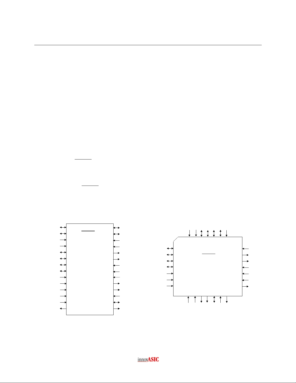
IA8251
28 Pin DIP
(28)
(27)
(26)
(25)
(24)
(23)
(22)
(21)
(20)
(19)
(18)
(17)
(16)
(15)
Package Pinout
D1
D0
VCC
RXC_n
DTR_n
RTS_n
DSR_n
RESET
CLK
TXD
TXEMPTY
CTS_n
SYNDET_BD
TXRDY
TXC_n
WR_n
CS_n
D6
D7
(5)D4
(6)D5
(7)
(8)
(9)
(10)
(11)
RXD
GND
(4)
(3)
28 Pin LCC
(12)
(13)
CD_n
RD_n
D2
D3
(2)
(1)
IA8251
(14)
(15)
TXRDY
RXRDY
VCC
D0
D1
(28)
(27)
(26)
(16)
(17)
(18)
CTS_n
TXEMPTY
SYNDET_BD
(25)
(24)
(23)
(22)
(21)
(20)
(19)
RXC_n
DTR_n
RTS_n
DSR_n
RESET
CLK
TXD
Copyright 1999, InnovASIC Inc.
Customer Specific IC Solutions
Page 2 of 4
IA8251 Advanced Information Sheet
Programmable Communication Interface
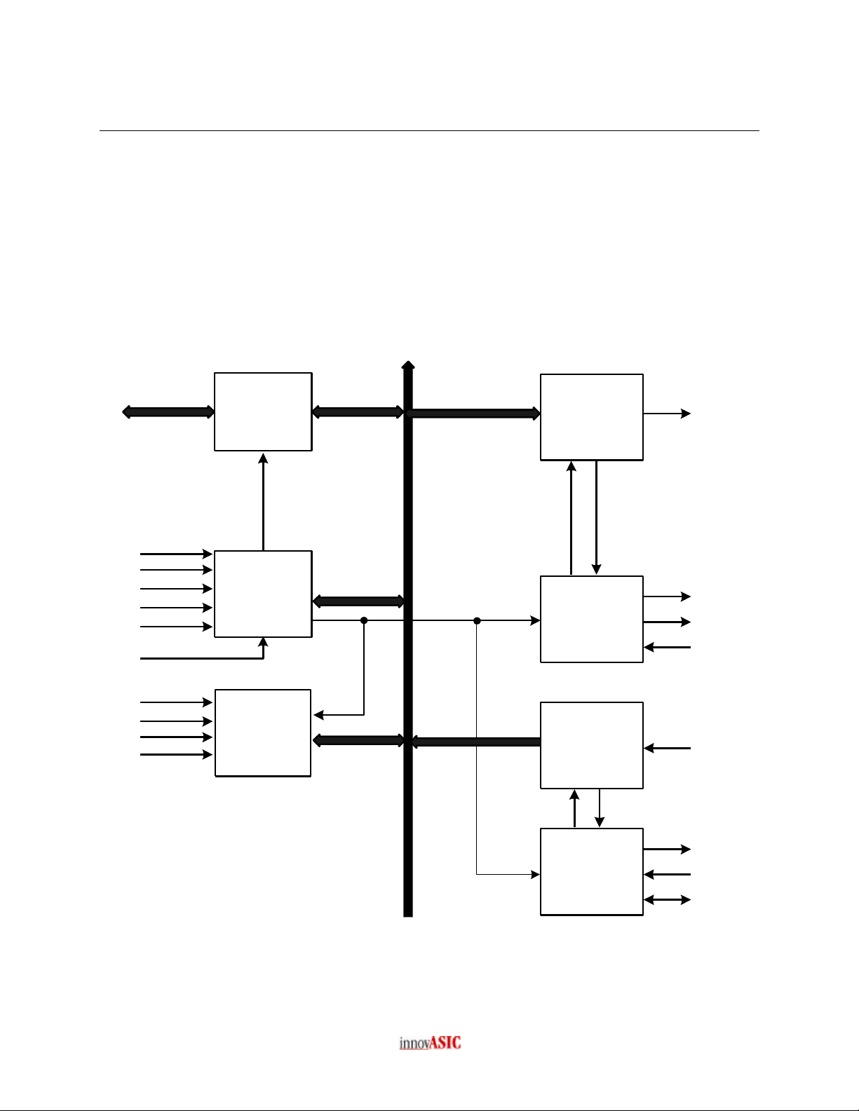
The IA8251 provides an interface between a microprocessor and a serial communications channel.
The IA8251 receives and transmits data in a variety of configurations including 7- or 8-bit data
words, with odd, even , or no parity, and 1 or 2 stop bits. The transmitter and receiver can be
designed for synchronous or asynchronous operation.
A block diagram is shown in Figure 1.
Functional Block Diagram
Figure 1
INTERNAL DATA
BUS
D7:D0
RESET
CLK
CD_n
RD_n
WR_n
CS_n
DSR_n
DTR_n
CTS_n
RTS_n
DATA BUS
BUFFER
READ/WRITE
CONTROL
LOGIC
MODEM
CONTROL
GROUP A
PORT A
(8)
GROUP A
PORT C
UPPER (4)
GROUP B
PORT C
LOWER
(4)
TXD
TXRDY
TXEMPTY
TXC_n
RXD
Copyright 1999, InnovASIC Inc.
Customer Specific IC Solutions
GROUP B
PORT B
(8)
RXRDY
RXC_n
SYNDET_BD
 Loading...