

INOVC IA82510-PDW28I-01, IA82510-PLC28I-01 Datasheet
IA82510 Data Sheet
ASYNCHRONOUS SERIAL CONTROLLER As of Production Ver. 01
FEATURES
• Form, Fit, and Function Compatible with the Intel 82510
• Packaging options available: 28 Pin Plastic or Ceramic DIP, 28 Pin Plastic
Leaded Chip Carrier, 28 Pin Ceramic Leadless Chip Carrier
• Asynchronous Serial Channel Operation
• Separate Transmit and Receive FIFOs with Programmable Threshold
• Programmable Baud Rate Generators up to 288K Baud
• Special Protocol Features
- Control Character Recognition
- Auto Echo and Loopback Modes
- 9-Bit Protocol Support
- 5 to 9 Bit Character Format
The IA82510 is a "plug-and-play" drop-in replacement for the original IC. innovASIC produces replacement ICs
using its MILESTM, or Managed IC Lifetime Extension System, cloning technology. This technology produces
replacement ICs far more complex than "emulation" while ensuring they are compatible with the original IC.
MILESTM captures the design of a clone so it can be produced even as silicon technology advances. MILESTM
also verifies the clone against the original IC so that even the "undocumented features" are duplicated. This data
sheet documents all necessary engineering information about the IA82510 including functional and I/O
descriptions, electrical characteristics, and applicable timing.
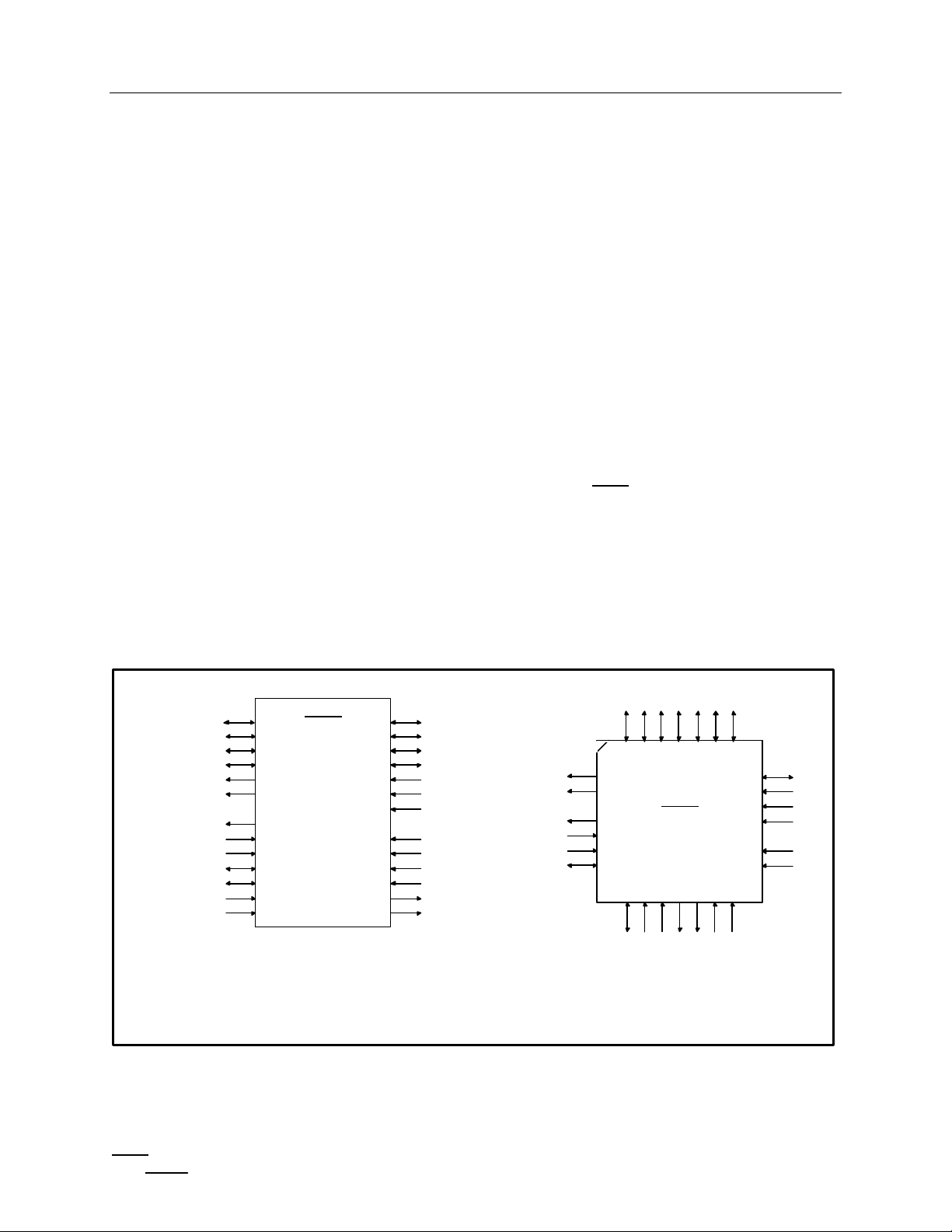
Package Pinout
(16)
RTSn
(17)
D1
(18)
RESET
CSn
(25)
(24)
(23)
(22)
(21)
(20)
(19)
D0
A2
A1
A0
VDD
RDn
WRn
IA82510
(1)D4
(2)D5
28 Pin DIP
(3)D6
(4)D7
(5)INT
(6)TXD
(7)VSS
(8)X2 or OUT2n
(9)X1 or CLK
(10)SCLK or RIn
(11)DSRn or TA or OUT0n
(12)DCDn or ICLK or OUT1n
(13)RXD
(14)CTSn
(28) D3
(27) D2
(26) D1
(25) D0
(24) A2
(23) A1
(22) A0
(21) VDD
(20) RDn
(19) WRn
(18) CSn
(17) RESET
(16) RTSn
(15) DTRn or TB
(4)D7(3)D6(2)D5(1)D4(28)D3(27)D2(26)
(5)INT
(6)TXD
(7)VSS
(8)X2 or OUT2n
(9)X1 or CLK
(10)SCLK or RIn
(11)DSRn or TA or OUT0n
IA82510
28 Pin LCC
(15)
(14)
(13)
(12)
RXD
CTSn
DTRn or TB
DCDn or ICLK or OUT1n
Copyright 2001 ENG211001219-01 www.innovasic.com
innovASIC Customer Support:
The End of Obsolescence Page 1 of 14 1-888-824-4184
IA82510 Data Sheet
CONFIG., STATUS, RXDATA
TIMING
(Baud Rate
PIN
RECEIVER
MODEM
X2 or OUT2n
RTSn
DSRn or TA or OUT0n
RDn
INT
ASYNCHRONOUS SERIAL CONTROLLER As of Production Ver. 01
DESCRIPTION
The IA82510 is an asynchronous serial controller that provides a CPU interface to one transmit
and one receive channel. It is Form, Fit, and Function compatible with the Intel 82510.
Configuration registers are used to control the serial channel, interrupts, and modes of operation.
The CPU controls this device via address and data lines with read/write control. The CPU also
uses this interface to read and write data to receive and transmit data through the serial channel.
FIFOs and various serial modes can be used to help off-load the CPU from transmitting and
receiving data. An interrupt line provides an indication to the CPU that the device requires
servicing. The device can be configured for 8250A/16450 compatibility.
Functional Block Diagram
IA82510
A(2:0)
D(7:0)
WRn
CSn
BUS INTERFACE
(Reset Logic,
Registers,
Interrupt Generation,
TRANSMITTER
TXD
RESET
Generators A & B,
Clocking
RXD
CTSn
CONFIGURATION
DCDn or ICLK or OUT1n
DTRn or TB
X1 or CLK
SCLK or RIn
Copyright 2001 ENG211001219-01 www.innovasic.com
innovASIC Customer Support:
The End of Obsolescence Page 2 of 14 1-888-824-4184

IA82510 Data Sheet
ASYNCHRONOUS SERIAL CONTROLLER As of Production Ver. 01
Functional Overview
Transmitter
The Transmit function consists of a 4 × 11 bit FIFO, and a Transmit Engine. The 4 × 11 FIFO is
configurable as any depth between one and four words inclusive. The transmit engine is
responsible for reading the data out of the FIFO and placing it in the proper order on the TXD pin.
The transmit engine is highly configurable to be compatible with numerous formats, including
16450 and 8250 modes of communication. Transmit Communication parameters that can be
programmed include:
• Parity modes
• Stop Bits
• Character Length
• FIFO Depth
• Clocking Options
• RTS and CTS modes
See the Register Description for more details.
Receiver
The Receiver function consists of a 4 × 11 configurable FIFO and a Receive Engine. The receive
engine is responsible for sampling the data on the RXD input pin, formatting the data, and placing
the data in the FIFO. The receive engine is highly configurable with parameters that include:
• Parity modes
• Stop Bits
• Character Length
• FIFO Depth
• Clocking Options
• Address Matching Options
• Control Character Detection
• RTS and CTS modes
See the Register Description for more details.
Bus Interface
The Bus Interface is a simple interface that allows a micro-processor or micro-controller to read
and write the IA82510 Registers. It consists of the following I/O lines:
• A0, A1, A2 : 3 Bit Address
• D0-D7 : 8 Bit Data
• RDn: Active Low Read Enable
• WRn: Active Low Write Enable
• CSn: Active Low Chip Select
• INT: Interrupt Output
• RESET: Chip Reset
Copyright 2001 ENG211001219-01 www.innovasic.com
innovASIC Customer Support:
The End of Obsolescence Page 3 of 14 1-888-824-4184
IA82510 Data Sheet
ASYNCHRONOUS SERIAL CONTROLLER As of Production Ver. 01
Register Description
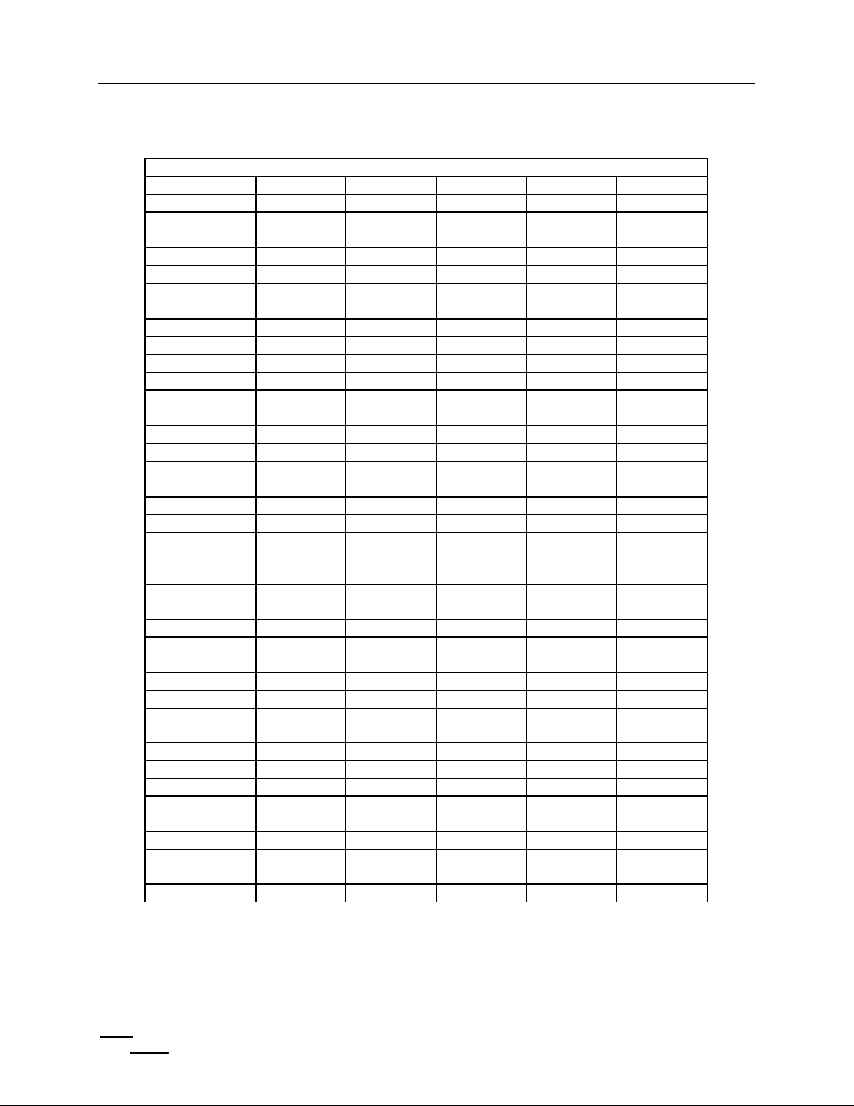
Table 1 – IA82510 Register Summary
Register ADDR Bank DLAB Mode Default
ACR0 111 00 X R/W 00000000
ACR1 101 10 X R/W 00000000
BACF 001 11 0 R/W 00000100
BAH 001 00 1 R/W 00000000
BAL 000 00 1 R/W 00000010
BANK 010 X X W 00000000
BBCF 011 11 X R/W 10000100
BBH 001 11 1 R/W 00000000
BBL 000 11 1 R/W 00000101
CLCF 000 11 0 R/W 00000000
FLR 100 01 X R 00000000
FMD 001 10 X R/W 00000000
GER 001 00 0 R/W 00000000
GIR_BANK 010 X X R 00000001
GSR 111 01 X R 00010010
ICM 111 01 X W N/A
IMD 100 10 X R/W 00001100
LCR 011 00 X R/W 00000000
LSR 101 00 X R/W 01100000
MCR 100
100
MIE 101 11 X R/W 00001111
MSR 110
110
PMD 100 11 X R/W 11111100
RCM 101 01 X W N/A
RIE 110 10 X R/W 00011110
RMD 111 10 X R/W 00000000
RST 101 01 X R 00000000
RXDATA 000
RXF 001 01 X R Unknown
TCM 110 01 X W N/A
TMCR 011 01 X W N/A
TMD 011 10 X R/W 00000000
TMIE 110 11 X R/W 00000000
TMST 011 01 X R 00110000
TXDATA 000
TXF 001 01 X W N/A
00
01
00
01
00
01
00
01
X
X
X
X
0
X
0
X
R/W
W
R/W
R
R Unknown
W N/A
00000000
00000000
Copyright 2001 ENG211001219-01 www.innovasic.com
innovASIC Customer Support:
The End of Obsolescence Page 4 of 14 1-888-824-4184

IA82510 Data Sheet
ASYNCHRONOUS SERIAL CONTROLLER As of Production Ver. 01
AC/DC Parameters
Absolute maximum ratings:
Supply Voltage, VDD…………………………….…-0.3V to +6.0V
Input Voltage, VIN…………………………………-0.3V to VDD +0.3V
Input Pin Current, IIN…………………………….±10 mA, 25° C
Operating Temperature Range……………………..-40° C to +85°C
Ambient temperature under bias........................……..-40°C to +85°C *
Storage temperature.......................................…........….- 55°C to +150°C
Lead Temperature………………………………….+300°C, 10 sec.
Power dissipation..............................................................155 mW, 125°C, 25MHz, 15% Toggle
Stresses beyond those listed under “absolute maximum ratings” may cause permanent damage to the device. Operating the device beyond the conditions
indicated in the “recommended operating conditions” section is not recommended. Operation at the “absolute maximum ratings” may adversely affect
device reliability.
* The input and output parametric values in section VII-B, parts 1, 2, and 3, are directly related to ambient
temperature and DC supply voltage. A temperature or supply voltage range other than those specified in the
Operating Conditions above will affect these values and part performance is not guaranteed by innovASIC.
Copyright 2001 ENG211001219-01 www.innovasic.com
innovASIC Customer Support:
The End of Obsolescence Page 5 of 14 1-888-824-4184
 Loading...