

INOVC IA64250-PLC68M Datasheet
IA64250 Data Sheet
Histogram/Hough Transform Processor As of Production Ver. 01
FEATURES
• Histogram and Hough Transform Calculation
• Four 512 X 9 Look-up Tables Provided to Perform User-defined Point -wise
Transformations
• Real-time Histogram Equalization
• High Data Rates
• 512 X 24 Accumulation RAM
• Pixel Location Function
The IA64250 is a "plug -and -play" drop -in replacement for the original LSI L64250. This replacement IC
has been developed using innovASIC’s MILESTM, or Managed IC Lifetime Extension System, cloning
technology. This technology produces replacement ICs far more complex than "emulation" while ensuring
they are compatible with the original IC. MILESTM captures the design of a clone so it can be produced even
as silicon technology advances. MILESTM also verifies the clone against the original IC so that even the
"undocumented features" are duplicated. This data sheet documents all necessary engineering information
about the IA64250 including functional and I/O descriptions, electrical characteristics, and applicable timing.
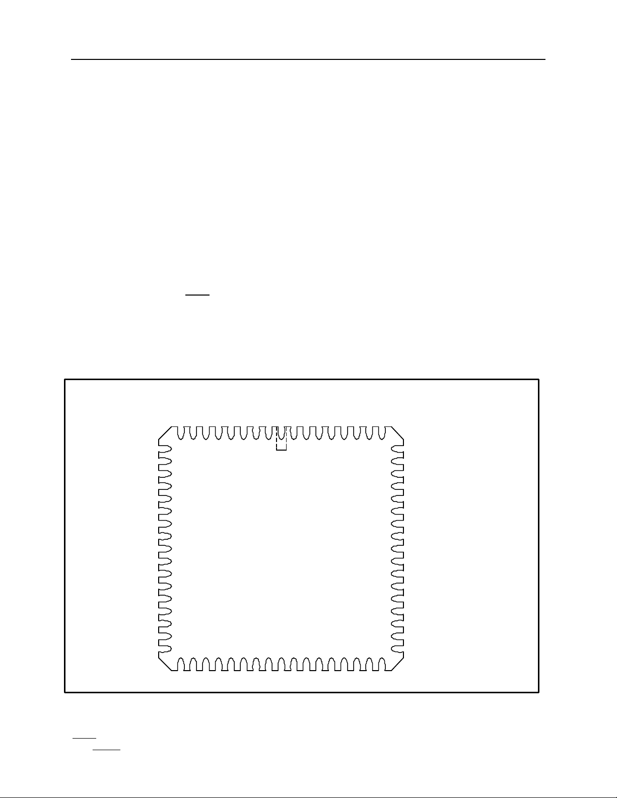
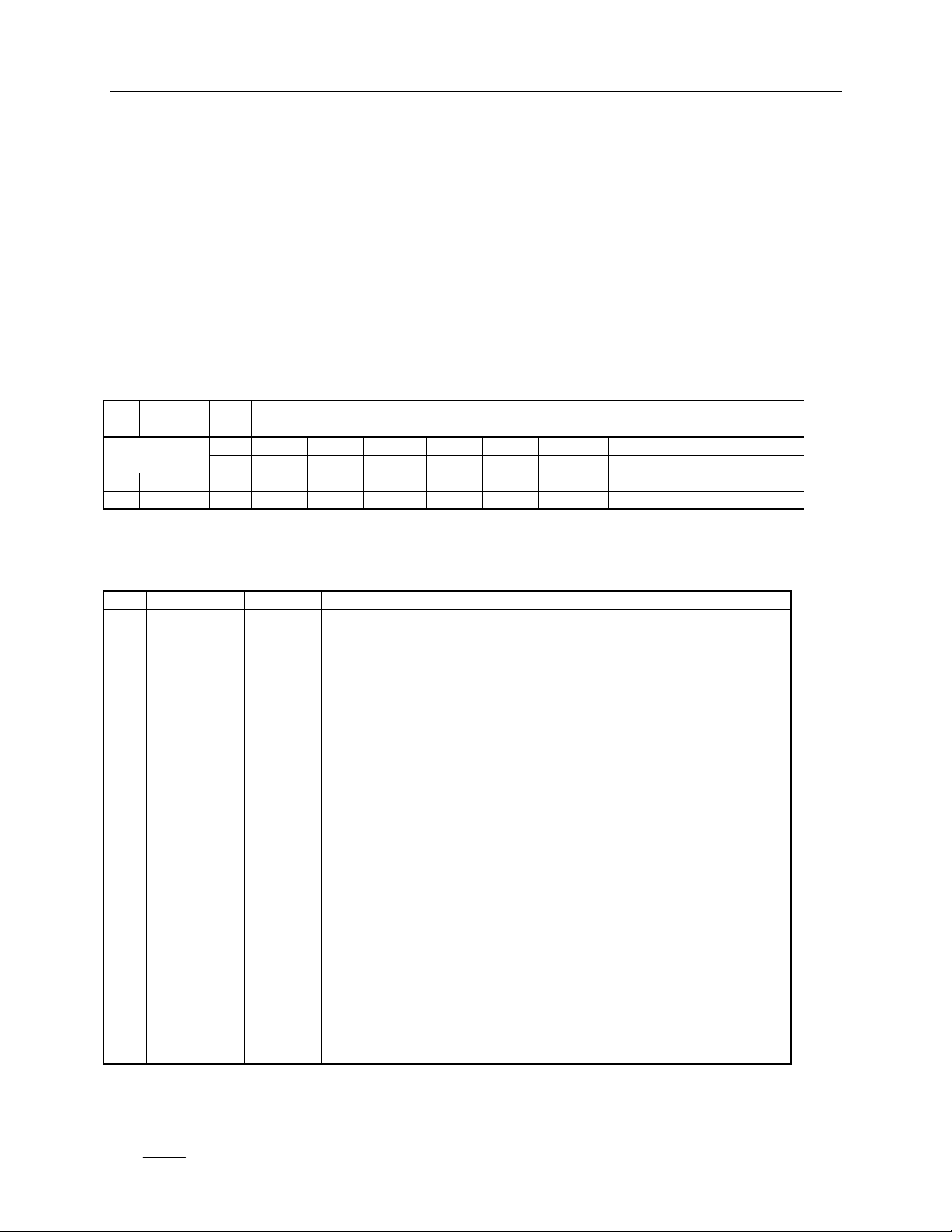
Package Pinout for 68 PLCC PACKAGE:
10
11
12
13
14
15
16
17
18
19
20
21
22
23
24
25
26
27 28 29 30 31 32 33 34 35 36 37 38 39 40 41 42 43
123456789
6162636465666768
60
59
58
57
56
55
54
53
52
51
50
49
48
47
46
45
44
Copyright 2000 ENG211001219-01 www.innovasic.com
innovASIC Customer Support:
The End of Obsolescence Page 1 of 21 1-888-824-4184
IA64250 Data Sheet
GRID #
Histogram/Hough Transform Processor As of Production Ver. 01
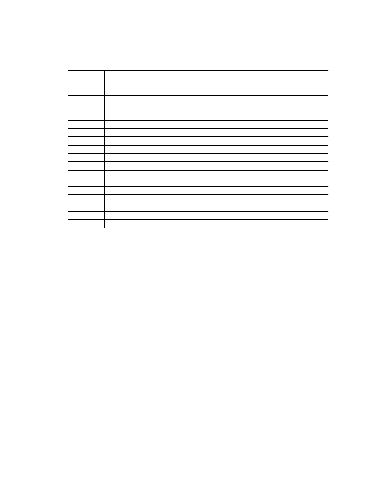
PIN DESIGNATOR:
PIN
NAME GRID #
GND 1 GND 18 GND 35 DO.5 52
CI.5 2 VDD 19 STARTIO 36 DO.6 53
CI.4 3 VDO.6 20 VDD 37 DO.7 54
CI.3 4 VDO.5 21 CLK2 38 DO.8 55
CI.2 5 VDO.4 22 PO 39 DI.0 56
CI.1 6 VDO.3 23 IODV 40 DI.1 57
CI.0 7 VDO.2 24 DV 41 DI.2 58
WE 8 VDO.1 25 AT 42 DI.3 59
REGADR.5 9 VDO.0 26 GND 43 DI.4 60
VDD 10 VDD 27 VDD 44 VDD 61
REGADR.4 11 RESET FP 28 DO.0 45 DI.5 62
REGADR.3 12 GND 29 DO.1 46 DI.6 63
REGADR.2 13 RY 30 DO.2 47 DI.7 64
REGADR.1 14 CY 31 DO.3 48 DI.8 65
REGADR.0 15 RX 32 DO.4 49 CI.8 66
VDO.8 16 CX 33 VDD 50 CI.7 67
VDO.7 17 CLK1 34 GND 51 CI.6 68
PIN
NAME
GRID #
PIN
NAME
PIN
NAME
GRID #
Copyright 2000 ENG211001219-01 www.innovasic.com
innovASIC Customer Support:
The End of Obsolescence Page 2 of 21 1-888-824-4184
IA64250 Data Sheet
Histogram/Hough Transform Processor As of Production Ver. 01
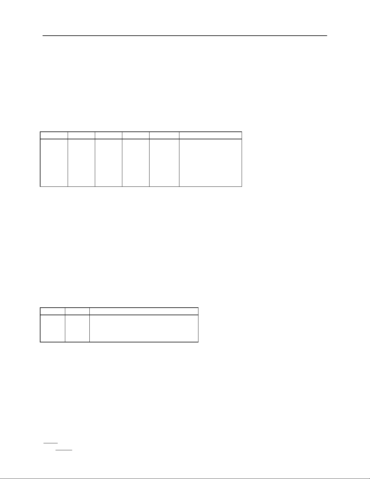
BLOCK DIAGRAM:
Figure 1
AT
REGADR
6
STARTIO_N
RESETFP
DI
9
CLOCK
IODV
CI
9
CONTROLLER
RAMADDR
RAMDATA
HCLR
SAT
SEL
LUT
LUTADDR
LUTDATA
OUT_SEL
2
MOD_RAMDATA
9
24
2
4
2
9
9
CY
CLOCK
RY
24
ACC RAM
512 X 24
LUT RAM
4 X 512 X 9
Y
COUNTER
24
CLOCK
CLOCK
LUTOUT
9
Y
SYNC
ADDER SYNC SHIFT
24
DV
ADDER SHIFT
9
10
24
9
DO
9
OUT_SEL
9
VDO
RESET
CLOCK
COUNTER
FP
9
FP
CX
CLOCK
RX
CI
AT
REGADR
X
COUNTER
MARKER
MEMORY
WE_N
X
9
MODE
Copyright 2000 ENG211001219-01 www.innovasic.com
innovASIC Customer Support:
The End of Obsolescence Page 3 of 21 1-888-824-4184

IA64250 Data Sheet
Histogram/Hough Transform Processor As of Production Ver. 01
Description
The IA64250 performs three separate tasks, histogram generation, modified Hough transforms, and
pixel location. There are three modes of operation for the IA64250: computation, I/O, and
initialization.
The controller block in the block diagram decodes the instructions and contains the mode registers.
After decoding the mode, the controller generates all of the control signals to the rest of the part.
These control signals include the addresses and input data for the LUT and ACC RAMs, the select
lines for both the output mux and the shifter, and the reset for the FP counter. This block also
controls the clearing of the ACC RAM.
The ACC RAM stores the video data that is to be output during the I/O mode. This data can be
modified, depending on mode, by several methods prior to being output. These methods are
described in the computation mode section.
The LUT RAM can store up to four different data modifying functions. These functions are used to
modify the video data coming in and access the appropriate data in the ACC RAM through the ACC
RAM address. This data is then sent out on the DO output.
During the initialization mode, the functions to be performed are defined. This is accomplished by
setting the values in the mode registers contained in the controller block.
During the computation mode, the histogram, Hough transform, or pixel location data is computed.
Data equalization also occurs during this mode if desired. The controller block controls the adders
and shifters during this mode to ensure correct data manipulation. This is accomplished through the
data stored in the mode registers as well as the DV input. The controller block also generates the
addresses to both the RAMs.
The I/O mode allows data to be transferred to the Accumulation RAM (ACC RAM) and/or to and
from the Look Up Table RAM (LUT RAM). The user can also update the marker memory during
the I/O mode. The marker memory is used to quickly find points of interest on the histogram,
Hough transform, or accumulated histogram curves. Up to seven points of interest can be specified
on the grey level axis or parameter axis. The corresponding value on the accumulation axis will then
be available. The reverse is also true, where the user can specify accumulation values of interest and
obtain the corresponding grey values. The memory map located in the I/O mode description shows
the configuration of the data stored in the memory. The transfer of data from an external source to
either of the RAMs is done through either the CI or DI input bus. The controller block takes in the
data and passes it along to the appropriate RAM. The controller block also supplies the RAM with
the address and control signals needed to write the data. During a data transfer from one RAM to
the other, the controller block performs a similar task, overseeing the transfer and supplying the
necessary control signals and address.
Copyright 2000 ENG211001219-01 www.innovasic.com
innovASIC Customer Support:
The End of Obsolescence Page 4 of 21 1-888-824-4184
IA64250 Data Sheet
Selects marker and maximum registers when HIGH or mode latches when LOW.
Histogram/Hough Transform Processor As of Production Ver. 01
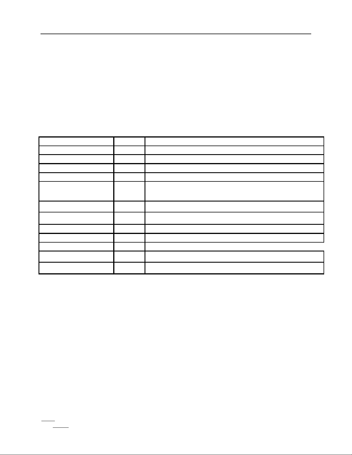
I/O SIGNAL DESCRIPTION:
The diagram below describes the I/O characteristics for each signal on the IC. The signal
names correspond to the signal names on the pinout diagrams provide.
I/O Characteristics:
IODV O When HIGH, ACC RAM or LUT RAM data on the DO bus is valid.
VDO.0 - VDO.8 O
CIO.0 - CIO.8 I
WE I Used to strobe data into mode latches when LOW.
REGADR.0 - REGADR.5 I Selects mode latch, marker or maximum registers.
LUT RAM data output (uses CLK1).
Control register and LUT input data bus.
AT I
CLK1 I
CLK2 I
AT must be LOW to access the LUT or ACC RAMs via the DO bus.
Pixel clock active at rising edge.
User I/O clock (may be connected to CLK1)
STARTIO I Initiates RAM I/O at HIGH to LOW transition.
CX,CY I Used to increment X or Y counters when HIGH.
RX,RY I
RESET FP I
PO O
Resets X or Y counters(overrides CX, CY) when HIGH.
Resets FP counter when HIGH.
Test pin should be left unconnected.
Copyright 2000 ENG211001219-01 www.innovasic.com
innovASIC Customer Support:
The End of Obsolescence Page 5 of 21 1-888-824-4184
IA64250 Data Sheet
Histogram/Hough Transform Processor As of Production Ver. 01
INITIALIZATION MODE:
Initialization defines the operation of the IA64250. The mode and marker memories store
66 nine-bit words that define the operation of the part and contain marker information. The
REGADR input is used to select the proper register. Data is written over the CI bus and
read on the DO bus. The AT pin controls whether data is a mode word or a marker. When
AT is low, the data written is mode information, which is stored in the mode registers
contained in the controller block. When AT is high, the data is a marker, and is stored in the
marker memory. To prevent erroneous operation STARTIOn should be high, and IODV
and DV should be low during initialization.
Mode Register Table:
AT REGA
DR
0 0 W sel0 sel1 sel2 sel3 lut0 lut1 sh1 sat TESTn
0 1 W fn0 fn1 Eq io0 io1 hclr0 hclr1 func pdwn
Marker Memory Table:
AT REGADR R/W CONTENTS
1
0
1
1
1
2
1
3
1
16
1
17
1
18
1
19
1
32
1
33
1
34
1
35
1
36
1
37
1
38
1
39
1
56
1
57
1
58
1
59
*ACC COUNT BIT 18-23 APPEARS ON BIT LOCATION 0-5 RESPECTIVELY
R/W BIT LOCATION
W ci0 ci1 ci2 ci3 ci4 ci5 ci6 ci7 ci8
R do0 do1 do2 do3 do4 do5 do6 do7 do8
R
R
R
R
W
W
W
W
R/W
R/W
R/W
R/W
R/W
R/W
R/W
R/W
R/W
R/W
R/W
R/W
GREY LEVEL OF MAXIMUM ACC COUNT BITS 0-8
MAXIMUM ACC COUNT BITS 0-8
MAXIMUM ACC COUNT BITS 9-17
MAXIMUM ACC COUNT BITS 18-23*
TEST MODE, DO NOT ACCESS
TEST MODE, DO NOT ACCESS
TEST MODE, DO NOT ACCESS
TEST MODE, DO NOT ACCESS
R/W MARKER 0 GREY LEVEL BITS 0-8
R/W MARKER 0 ACC COUNT BITS 0-8
R/W MARKER 0 ACC COUNT BITS 9-17
R/W MARKER 0 ACC COUNT BITS 18-23*
R/W MARKER 1 GREY LEVEL BITS 0-8
R/W MARKER 1 ACC COUNT BITS 0-8
R/W MARKER 1 ACC COUNT BITS 9-17
R/W MARKER 1 ACC COUNT BITS 18-23*
.
.
.
R/W MARKER 6 GREY LEVEL BITS 0-8
R/W MARKER 6 ACC COUNT BITS 0-8
R/W MARKER 6 ACC COUNT BITS 9-17
R/W MARKER 6 ACC COUNT BITS 18-23*
Copyright 2000 ENG211001219-01 www.innovasic.com
innovASIC Customer Support:
The End of Obsolescence Page 6 of 21 1-888-824-4184
IA64250 Data Sheet
Histogram/Hough Transform Processor As of Production Ver. 01
Mode Definition:
The controller block decodes the instructions brought in to the IA64250 on the CI bus, with
the REGADR input determining which instructions are being read in. The Mode Memory
table shows the configuration of the CI bus encoded instruction depending on the state of
REGADR. A brief description of the instruction bits follows:
sel(3:0) selects the nine bits of the ACC RAM to be transferred to the DO output or to the LUT
RAM.
sel0 sel1 sel2 sel3 Sel window
0
1
0
1
0
…
1
lut(1:0) defines one of the four 512 X 9 LUTs as active.
sh1 When low, the least significant nine bits of the 10 bit LUT and Y count sum will address the
sat When high, the nine bits selected from the 24 bit ACC RAM output will be forced to 511
test Used for testing when low. Should be high for normal operation.
fn(1:0) Determines the operation performed during the computational mode.
fn0 fn1 FUNCTION
0
0
1
1
eq When high, causes the output of the ACC RAM to be accumulated as it is read. This is
0
0
1
1
0
1
0
0
0
0
1
1
0
0
0
0
0
1
0
1
2
3
4
15
select bits 0-8
select bits 1-9
select bits 2-10
select bits 3-11
select bits 4-12
select bits 15-23
ACC RAM. When high, the nine most significant bits of the sum will be used.
(111111111) if the 24 bit ACC RAM output contains a 1 in the range of bits from the sel + 9
to 23. Otherwise the nine bits selected from the ACC RAM output will be unchanged.
0
1
0
1
modified Hough transform computation
undefined
histogram computation
pixel location
commonly used to compute the histogram equalization transfer function. When low, the
ACC RAM output is not modified.
Copyright 2000 ENG211001219-01 www.innovasic.com
innovASIC Customer Support:
The End of Obsolescence Page 7 of 21 1-888-824-4184
 Loading...