

INOVC IA16450-PDW40C, IA16450-PDW40I, IA16450-PLC44C, IA16450-PLC44I Datasheet
Page 1 of 10
IA16450 Preliminary Data Sheet
Universal Asynchronous Receiver/Transmitter
FEATURES
• Form, Fit, and Function Compatible with the National NS16450
• Packaging options available: 40 Pin Plastic or 44 Pin Plastic Leaded Chip
Carrier
• Programmable Word Length, Stop Bits, and Parity
• Full Duplex Operation
• Programmable Baud Rate Generator
- Division of any input clock by 1 to (216 –1)
- Generates Internal 16 x clock
• Programmable Serial-Interface
- 5-, 6-, 7- or 8-bit characters
- Even, Odd, or No-Parity Bit Generation and Detection
- 1-, 1 ½-, or 2-Stop Bit Generation
- Baud Generation of DC to 56k
• Prioritized Interrupt Control
• Internal Diagnostic/Loopback Capabilities
The IA16450 uses innovASIC’s innovative new f 3 Program to provide industry with parts that
other vendors have declared obsolete. By specifying parts through this program a customer is
assured of never having a component become obsolete again. This advanced information sheet
assumes the original part has been designed in, and so provides a summary of capabilities only. For
new designs contact innovASIC for more detailed information.
National is a copyright trademark of National Semiconductor Corporation
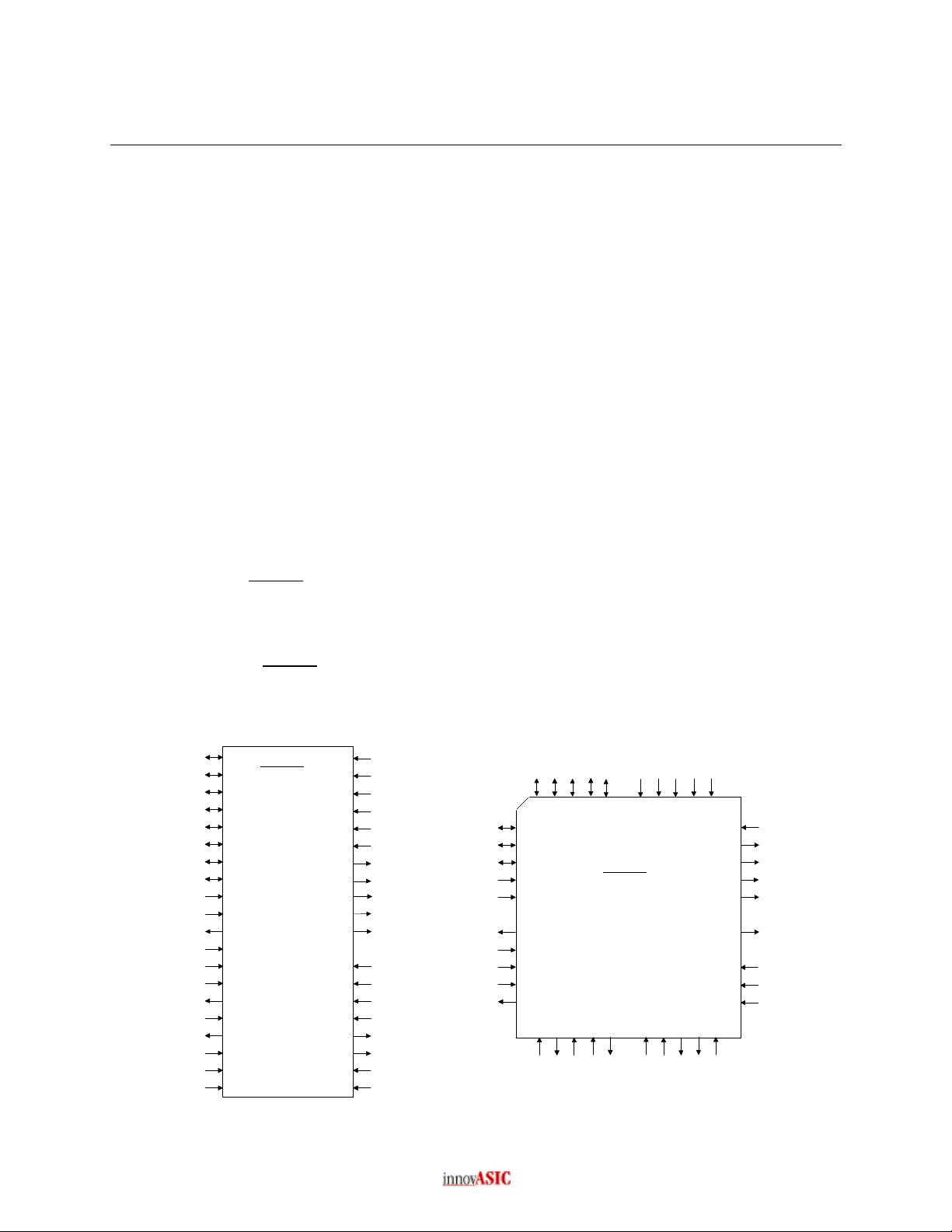
Package Pinout
D0
D1
D2
D3
D4
D5
D6
D7
CS2_n
(1)
(2)
(3)
(4)
(5)
(6)
(7)
(8)
(9)RCLK
(10)SIN
(11)SOUT
(12)CS0
(13)CS1
(14)
(15)BAUDOUT_n
(16)XIN
(17)XOUT
(18)WR_n
(19)WR
(20)VSS
IA16450
40 Pin DIP
(40)
(39)
(38)
(37)
(36)
(35)
(34)
(33)
(32)
(31)
(30)
(29)
(28)
(27)
(26)
(25)
(24)
(23)
(22)
(21)
VCC
RI_n
DCD_n
DSR_n
CTS_n
MR
OUT1_n
DTR_n
RTS_n
OUT2_n
INTR
N. C.
A0
A1
A2
ADS_n
CSOUT
DDIS
RD
RD_n
D3
D4
D2
D1
(6)
(5)
(4)
(19)
XOUT
(3)
44 Pin LCC
(20)
(21)
WR
WR_n
(7)D5
(8)D6
(9)D7
(10)RCLK
(11)SIN
(12)N. C.
(13)SOUT
(14)CS0
(15)CS1
(16)CS2_n
(17)BAUDOUT_n
(18)
XIN
D0
N. C.
(2)
(1)
IA16450
(22)
(23)
VSS
N. C.
VCC
(44)
(24)
RD_n
RI_n
(43)
(25)
RD
(42) DCD_n
(41) DSR_n
(26)
DDIS
(40) CTS_n
(39)
(38)
(37)
(36)
(35)
(34)
(33)
(32)
(31)
(30)
(29)
(27)
(28)
ADS_n
CSOUT
MR
OUT1_n
DTR_n
RTS_n
OUT2_n
N. C.
INTR
N. C.
A0
A1
A2
Copyright 1999, InnovASIC Inc.
Customer Specific IC Solutions
Page 2 of 10
IA16450 Preliminary Data Sheet
Universal Asynchronous Receiver/Transmitter
The IA16450 is a form, fit and function compatible part to the National NS16450 Univeral
Asynchronous Receiver/Transmitter. The IA16450 function receives and transmits data in a variety
of configurations including 5, 6, 7 or 8 bit data words, odd, even or no parity, and 1, 1.5, and 2 stop
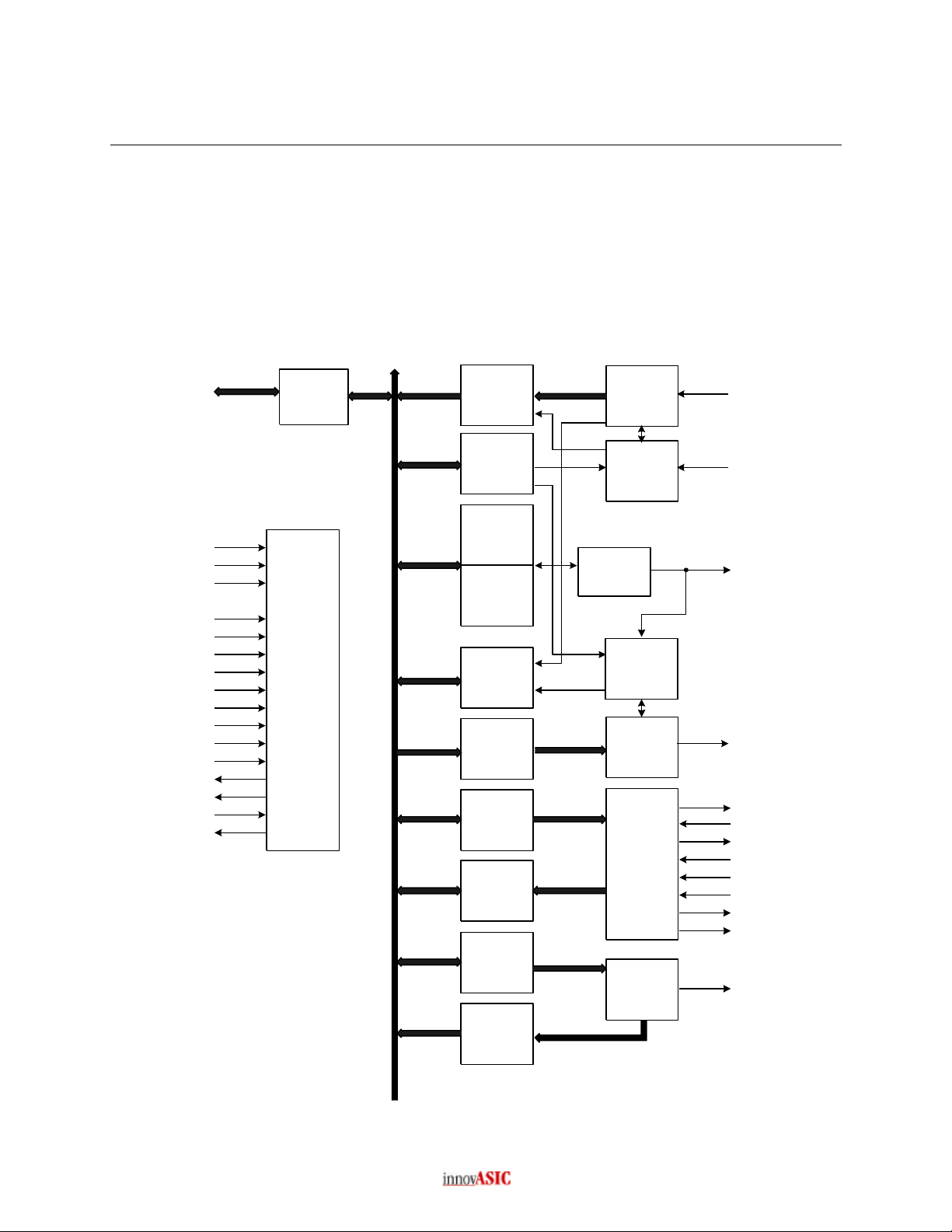
bits. This megafunction includes an internal Baud Rate Generator and Interrupt Control. A block
diagram is shown in Figure 1.
Functional Block Diagram
Figure 1
INTERNAL DATA
BUS
D7:D0
DATA BUS
BUFFER
RECEIVER
BUFFER
REGISTER
RECEIVER
SHIFT
REGISTER
SIN
A0
A1
A2
CS0
CS1
CS2_n
ADS_n
MR
RD
RD_n
WR
WR_n
DDIS
CSOUT
XIN
XOUT
DECODE
AND
CONTROL
LOGIC
LINE CONTROL
REGISTER
DIVISOR LATCH
(LSB)
DIVISOR LATCH
(MSB)
LINE STATUS
REGISTER
TRANSMITTER
HOLDING
REGISTER
MODEM
CONTROL
REGISTER
MODEM STATUS
REGISTER
RECEIVER
CONTROL
BAUD
GENERATOR
TRANSMITTER
TIMING
CONTROL
TRANSMITTER
REGISTER
MODEM
CONTROL
TIMING
&
&
SHIFT
LOGIC
RCLK
BAUDOUT_n
SOUT
RTS_n
CTS_n
DTR_n
DSR_n
DCD_n
RI
OUT1_n
OUT2_n
INTERRUPT
ENABLE
REGISTER
INTERRUPT ID
REGISTER
Copyright 1999, InnovASIC Inc.
Customer Specific IC Solutions
INTERRUPT
CONTROL
LOGIC
INTR
Page 3 of 10
IA16450 Preliminary Data Sheet
Universal Asynchronous Receiver/Transmitter
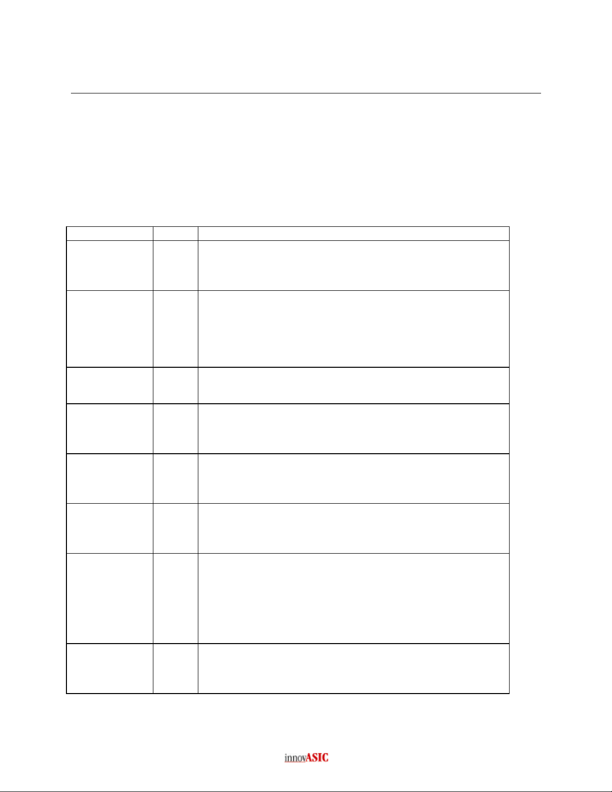
I/O Signal Description
Table 1 below describes the I/O characteristics for each signal on the IC. The signal names
correspond to the signal names on the pinout diagrams provided. Table 2 refers to the address
register map. Table 3 refers to the Preliminary A. C. Characteristics. Figure 2 illustrates the
Preliminary Timing Waveforms for this device. Environmental/Qualification Levels are listed in
Table 4.
Table 1
Name Type Description
MR I Master Reset - Active high - Clears all registers (except the
receiver buffer, transmitter holding and divisor latches) to their
initial state. Resets internal control logic to its initial state
A(2:0) I Register Address - Active high - This bus selects one of the
internal UART registers (refer to table 1). Note the state of the
divisor latch access bit (DLAB - the msb of the line control
register) must be set high to access the divisor latches and low
to access the receiver buffer or the interrupt enable register.
DIN(7:0) I Data Input Bus - Active high - Serves as input data when
writing to internal UART registers.
CS0 I Chip Select 0 - Active high - When CS0, CS1 and CS2 are active
the megafunction is selected. Read and write transactions to
internal UART registers are then possible.
CS1 I Chip Select 1 - Active high - When CS0, CS1 and CS2 are active
the megafunction is selected. Read and write transactions to
internal UART registers are then possible.
CS2_n I Chip Select 2 - Active low - When CS0, CS1 and CS2 are active
the megafunction is selected. Read and write transactions to
internal UART registers are then possible.
ADS_n I Address Strobe - Active low - Gating signal to the Address
input latch. The positive edge of ADS_n latches the state of the
register address bus into the Address input latch. If address
signals are guaranteed to be stable for the duration of a read or
write cycle, ADS_n may be tied low thus forcing the Address
input latch to be transparent.
RD I Read Control - Active High - when RD is high or RD_n is low
and the UART is selected, read transactions from internal
UART registers are possible.
Copyright 1999, InnovASIC Inc.
Customer Specific IC Solutions
 Loading...