

Page 1
PRODUCT SPECIFICATION
Customer:
Doc. Number:
□ Tentative Specification
□ Preliminary Specification
▓ Approval Specification
MODEL NO.: N140BGE
SUFFIX: P23
APPROVED BY SIGNATURE
Name / Title
Note
Please return 1 copy for your confirmation with your
signature and comments.
Approved By Checked By Prepared By
楊竣傑
楊竣傑
楊竣傑楊竣傑
2013-06-08
15:50:37 CST
曹文彬
曹文彬
曹文彬曹文彬
2013-05-30
17:24:27 CST
王淑玲
王淑玲
王淑玲王淑玲
2013-05-29
19:00:47 CST
Version 2.0 11 June 2013 1 / 28
The copyright belongs to InnoLux. Any unauthorized use is prohibited.
Page 2

PRODUCT SPECIFICATION
CONTENTS
1. GENERAL DESCRIPTION.........................................................................................................4
1.1 OVERVIEW ................................................................................................................................4
1.2 GENERAL SPECIFICATI0NS ...................................................................................................4
2. MECHANICAL SPECIFICATIONS .............................................................................................4
2.1 CONNECTOR TYPE..................................................................................................................4
2.1.2 LED Light-Bar Connector....................................................................................................5
3. ABSOLUTE MAXIMUM RATINGS .............................................................................................6
3.1 ABSOLUTE RATINGS OF ENVIRONMENT ..........................................................................6
3.2 ABSOLUTE RATINGS OF ENVIRONMENT(OPEN CELL) ..................................................6
3.3 ELECTRICAL ABSOLUTE RATINGS(OPEN CELL) .............................................................7
3.3.1 TFT LCD MODULE............................................................................................................7
4. ELECTRICAL SPECIFICATIONS...............................................................................................8
4.1 FUNCTION BLOCK DIAGRAM...............................................................................................8
4.2. INTERFACE CONNECTIONS .................................................................................................8
4.3 ELECTRICAL CHARACTERISTICS......................................................................................10
4.3.1 LCD ELETRONICS SPECIFICATION.............................................................................10
4.3.2 LED CONVERTER SPECIFICATION..............................................................................12
4.4 LVDS INPUT SIGNAL TIMING SPECIFICATIONS .........................................................14
4.4.1 LVDS DC SPECIFICATIONS ...........................................................................................14
4.4.2 LVDS DATA FORMAT......................................................................................................14
4.4.3 COLOR DATA INPUT ASSIGNMENT ............................................................................15
4.5 DISPLAY TIMING SPECIFICATIONS ...................................................................................16
4.6 POWER ON/OFF SEQUENCE ................................................................................................17
5. OPTICAL CHARACTERISTICS ...............................................................................................18
5.1 TEST CONDITIONS.................................................................................................................18
5.2 OPTICAL SPECIFICATIONS ..................................................................................................18
6. PACKING..................................................................................................................................22
6.1 INNOLUX OPEN CELL LABEL.............................................................................................22
6.2 CARTON...................................................................................................................................23
6.3 PALLET.....................................................................................................................................24
6.4 UNPACKING ............................................................................................................................25
7. PRECAUTIONS........................................................................................................................26
7.1 HANDLING PRECAUTIONS..................................................................................................26
7.2 STORAGE PRECAUTIONS ....................................................................................................26
7.3 OPERATION PRECAUTIONS.................................................................................................26
Appendix. OUTLINE DRAWING..................................................................................................27
Version 2.0 11 June 2013 2 / 28
The copyright belongs to InnoLux. Any unauthorized use is prohibited.
Page 3
REVISION HISTORY
PRODUCT SPECIFICATION
Version
2.0 May. 22, 2013
Date Page Description
All Approval Spec Ver.2.0 was first issued.
Version 2.0 11 June 2013 3 / 28
The copyright belongs to InnoLux. Any unauthorized use is prohibited.
Page 4
PRODUCT SPECIFICATION
Pin1 Pin40
1. GENERAL DESCRIPTION
1.1 OVERVIEW
N140BGE-P23 is a 14.0” (14.0” diagonal) TFT Liquid Crystal Display module with LED Backlight unit
and 40 pins LVDS interface. This module supports 1366 x 768 HD mode and can display 262,144
colors. The optimum viewing angle is at 6 o’clock direction.
1.2 GENERAL SPECIFICATI0NS
Item Specification Unit Note
Screen Size 14.0” diagonal
Driver Element a-si TFT active matrix - Pixel Number 1366 x R.G.B. x 768 pixel Pixel Pitch 0.2265 (H) x 0.2265 (V) mm Pixel Arrangement RGB vertical stripe - Display Colors 262,144 color Transmissive Mode Normally white - Surface Treatment Hard coating (3H), Glare - -
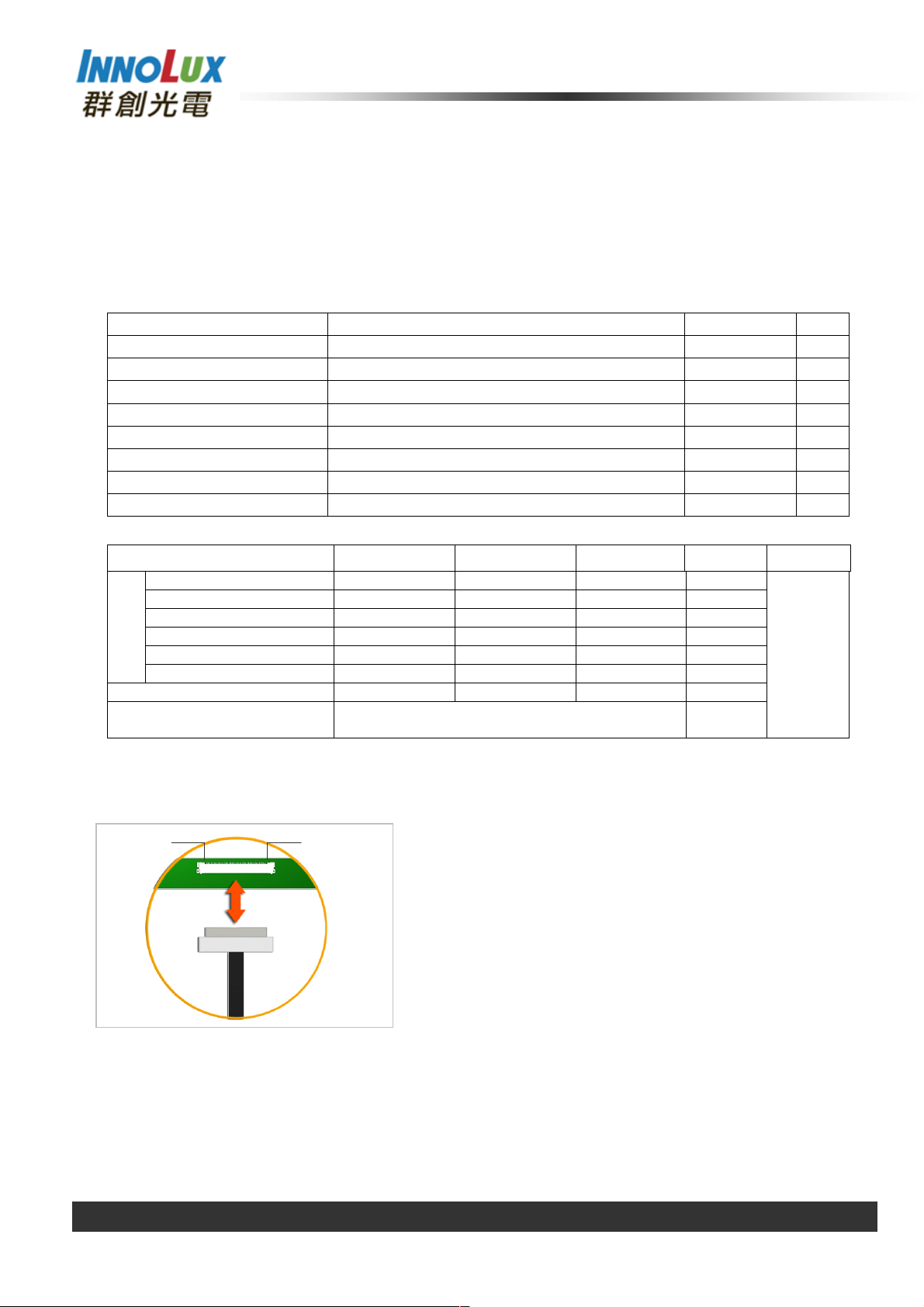
2. MECHANICAL SPECIFICATIONS
item Min. Typ. Max. Unit Note
Horizontal (H) with PCB 318.39 318.49 318.59 mm
Horizontal (H) w/o PCB 318.39 318.49 318.59 mm
Vertical (V) with PCB 223.65 224.65 225.65 mm
Size
Vertical (V) w/o PCB 182.75 182.85 182.95 mm
Thickness (T) with PCB - - 1.65 mm
Thickness (T) w/o PCB 1.21 1.27 1.33 mm
Weight - 170 180 -
I/F connector mounting position
Note (1) Please refer to the attached drawings for more information of front and back outline dimensions.
The mounting inclination of the connector makes
the screen center within ±0.5mm as the horizontal.
(1) (2)
g
(2) Connector mounting position
2.1 CONNECTOR TYPE
Please refer Appendix Outline Drawing for detail design.
Connector Part No.: IPEX-20455-040E-12 or TYCO 5-2069716-3.
User’s connector Part No: IPEX-20453-040T-01.
Version 2.0 11 June 2013 4 / 28
The copyright belongs to InnoLux. Any unauthorized use is prohibited.
Page 5
PRODUCT SPECIFICATION
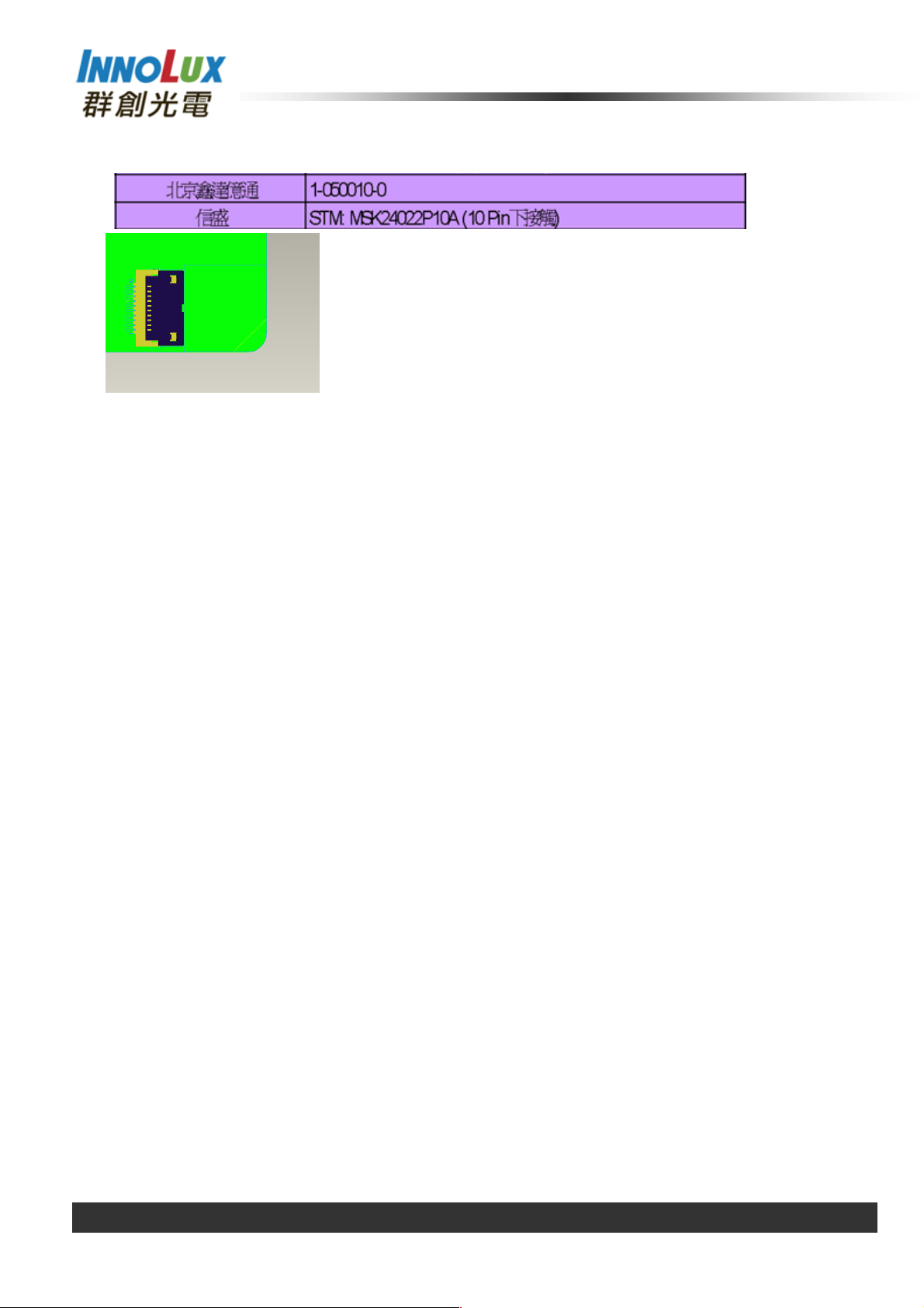
2.1.2 LED Light-Bar Connector
Version 2.0 11 June 2013 5 / 28
The copyright belongs to InnoLux. Any unauthorized use is prohibited.
Page 6
PRODUCT SPECIFICATION
3. ABSOLUTE MAXIMUM RATINGS
3.1 ABSOLUTE RATINGS OF ENVIRONMENT
Item Symbol
Min. Max.
Storage Temperature TST -20 +60 ºC (1)
Operating Ambient Temperature TOP 0 +50 ºC (1), (2)
Note (1) (a) 90 %RH Max. (Ta <= 40 ºC).
(b) Wet-bulb temperature should be 39 ºC Max. (Ta > 40 ºC).
(c) No condensation.
Note (2) The temperature of panel surface should be 0 ºC min. and 60 ºC max.
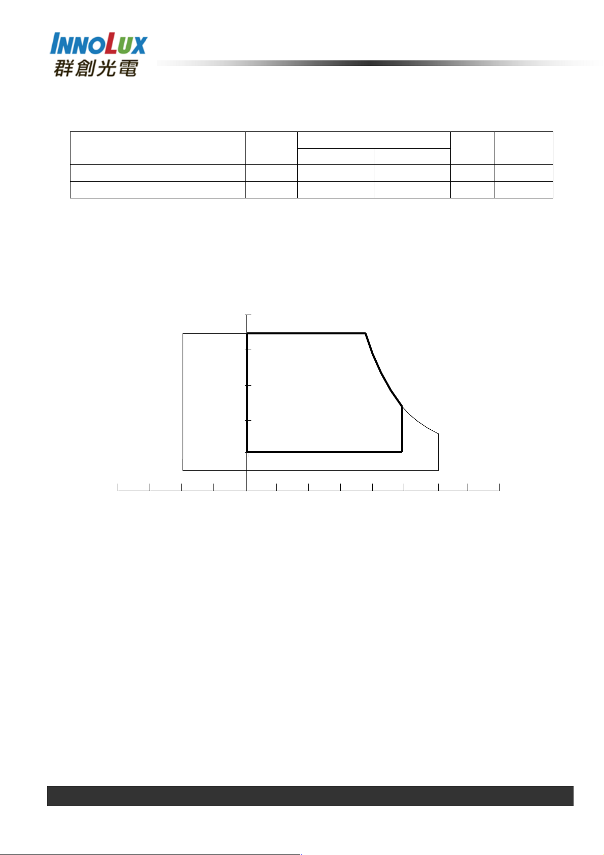
Relative Humidity (%RH)
100
90
80
Value
Unit Note
60
Operating Range
40
20
10
Storage Range
80 60 -20 40 0 20 -40
Temperature (ºC)
3.2 ABSOLUTE RATINGS OF ENVIRONMENT(OPEN CELL)
High temperature or humidity may reduce the performance of panel. Please store LCD panel within
the specified storage conditions.
Storage Condition: With packing.
Storage temperature range: 25±5 ºC.
Storage humidity range: 50±10%RH.
Shelf life: 30days
Version 2.0 11 June 2013 6 / 28
The copyright belongs to InnoLux. Any unauthorized use is prohibited.
Page 7
PRODUCT SPECIFICATION
3.3 ELECTRICAL ABSOLUTE RATINGS(OPEN CELL)
3.3.1 TFT LCD MODULE
Item Symbol
Power Supply Voltage VCCS -0.3 +4.0 V
Logic Input Voltage VIN -0.3 VCCS+0.3
Converter Input Voltage
Converter Control Signal Voltage
Converter Control Signal Voltage
Note (1) Stresses beyond those listed in above “ELECTRICAL ABSOLUTE RATINGS” may cause
permanent damage to the device. Normal operation should be restricted to the conditions
described in “ELECTRICAL CHARACTERISTICS”.
LED_VCCS
LED_PWM,
LED_EN
Value
Min. Max.
-0.3 26.0 V (1)
-0.3 5.0 V (1)
-0.3 5.0 V (1)
Unit Note
(1)
V
Version 2.0 11 June 2013 7 / 28
The copyright belongs to InnoLux. Any unauthorized use is prohibited.
Page 8
PRODUCT SPECIFICATION
DC/DC CONVERTER &
INPUT CONNECTOR
EDID
EEPROM
SCAN DRIV
ING CIRCUIT
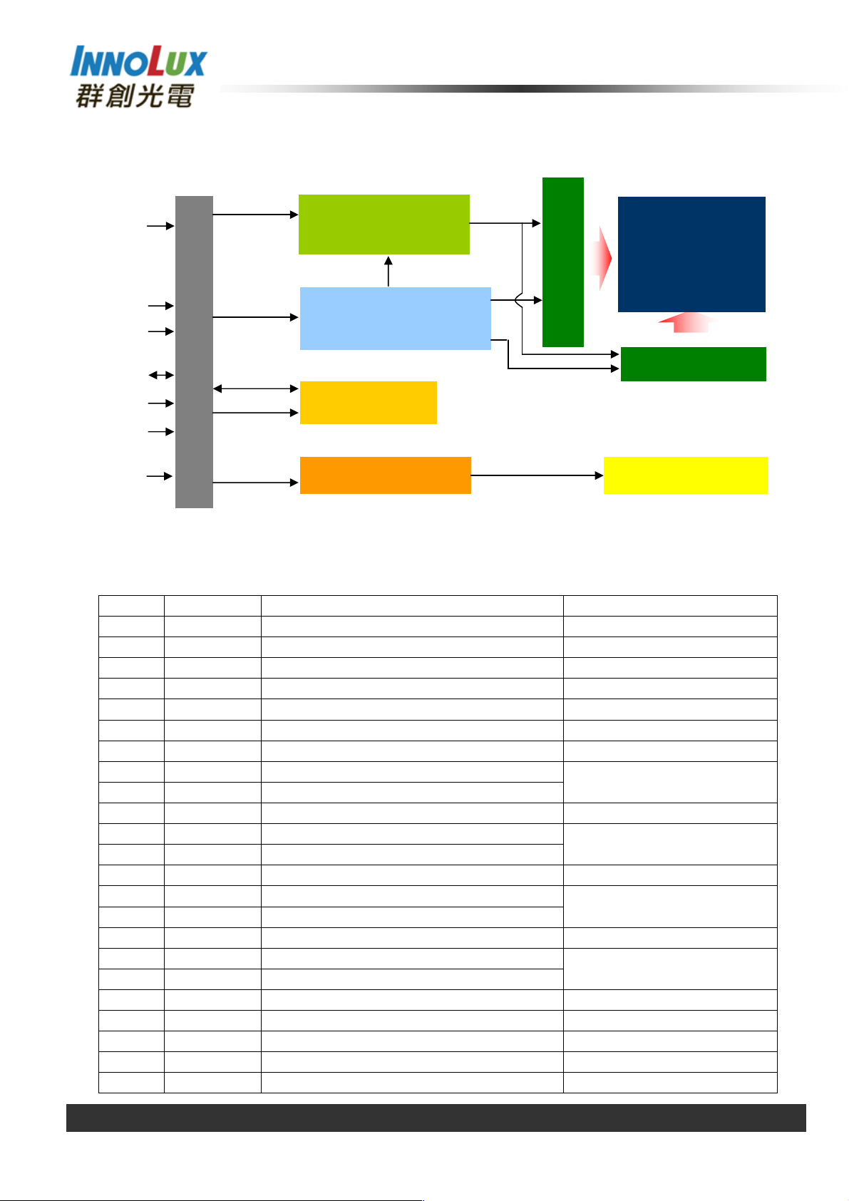
4. ELECTRICAL SPECIFICATIONS
4.1 FUNCTION BLOCK DIAGRAM
VCCS
GND
Data
EDID
CLK
EDID
V
EDID
Converter
Input Signals
REFERENCE VOLTAGE
LED CONVERTER BACKLIGHT UNIT
TIMING
CONTROLLER
GENERATOR
TFT LCD
PANEL
DATA DRIVER IC
4.2. INTERFACE CONNECTIONS
PIN ASSIGNMENT
Pin Symbol Description Remark
1 NC No Connection (Reserve)
2 VCCS Power Supply (3.3V typ.)
3 VCCS Power Supply (3.3V typ.)
4 VEDID DDC 3.3V power
5 NC No Connection (Reserved for INNOLUX test)
6 CLKEDID DDC clock
7 DATAEDID DDC data
8 Rxin0- LVDS differential data input
9 Rxin0+ LVDS differential data input
10 VSS Ground
11 Rxin1- LVDS differential data input
12 Rxin1+ LVDS differential data input
13 VSS Ground
14 Rxin2- LVDS Differential Data Input
15 Rxin2+ LVDS Differential Data Input
16 VSS Ground
17 RxCLK- LVDS differential clock input
18 RxCLK+ LVDS differential clock input
19 VSS Ground
20 NC No Connection (Reserve)
21 NC No Connection (Reserve)
22 VSS Ground
23 NC No Connection (Reserve)
R0-R5, G0
G1~G5, B0, B1
B2-B5,HS,VS, DE
LVDS CLK
Version 2.0 11 June 2013 8 / 28
The copyright belongs to InnoLux. Any unauthorized use is prohibited.
Page 9
PRODUCT SPECIFICATION
Pitch
24 NC No Connection (Reserve)
25 VSS Ground
26 NC No Connection (Reserve)
27 NC No Connection (Reserve)
28 VSS Ground
29 NC No Connection (Reserve)
30 NC No Connection (Reserve)
31 LED_GND LED Ground
32 LED_GND LED Ground
33 LED_GND LED Ground
34 NC No Connection (Reserve)
35 LED_PWM PWM Control Signal of LED Converter
36 LED_EN Enable Control Signal of LED Converter
37 NC No Connection (Reserve)
38 LED_VCCS LED Power Supply
39 LED_VCCS LED Power Supply
40 LED_VCCS LED Power Supply
Note (1) The first pixel is odd as shown in the following figure.
1,1
(odd)
2,1
1,2
(even)
2,2
1,3
(odd)
1,4
(even)
1,Xmax
3,1
Pitch
Ymax,1
Ymax,
Xmax
Version 2.0 11 June 2013 9 / 28
The copyright belongs to InnoLux. Any unauthorized use is prohibited.
Page 10

PRODUCT SPECIFICATION
4.3 ELECTRICAL CHARACTERISTICS
4.3.1 LCD ELETRONICS SPECIFICATION
Parameter Symbol
Min. Typ. Max.
Power Supply Voltage VCCS 3.0 3.3 3.6 V (1)
Ripple Voltage VRP - 50 - mV (1)
Value
Unit Note
Inrush Current I
- - 1.5 A (1),(2)
RUSH
Mosaic - 206 224 mA (3)a
Power Supply Current
Black
lcc
- 201 219 mA (3)
Note (1) The ambient temperature is Ta = 25 ± 2 ºC.
Note (2) I
: the maximum current when VCCS is rising
RUSH
IIS: the maximum current of the first 100ms after power-on
Measurement Conditions: Shown as the following figure. Test pattern: black.
+3.3V
Q1 2SK1475
VR1
R1
47K
47K
R2
1K
0.01uF
Q2
2SK1470
C2
(High to Low)
(Control Signal)
SW
+12V
C1
1uF
FUSE
C3
1uF
VCCS
(LCD Module Input)
VCCS rising time is 0.5ms
Version 2.0 11 June 2013 10 / 28
The copyright belongs to InnoLux. Any unauthorized use is prohibited.
Page 11

PRODUCT SPECIFICATION
Note (3) The specified power supply current is under the conditions at VCCS = 3.3 V, Ta = 25 ± 2 ºC, DC
Current and fv = 60 Hz, whereas a specified power dissipation check pattern is displayed
a. Mosaic Pattern
Active Area
Version 2.0 11 June 2013 11 / 28
The copyright belongs to InnoLux. Any unauthorized use is prohibited.
Page 12

PRODUCT SPECIFICATION
PWM Control Permissive Ripple
C2
4.3.2 LED CONVERTER SPECIFICATION
Parameter Symbol
Value
Unit Note
Min. Typ. Max.
Converter Input power supply voltage
Converter Inrush Current
LED_Vccs
ILED
RUSH
5.0 12.0 21.0 V
- - 1.5 A (1)
Backlight On 2.2 - 3.6 V
EN Control Level
Backlight Off
PWM High Level
PWM Control Level
PWM Low Level
0 - 0.6 V
2.2 - 3.6 V
0 - 0.6 V
PWM Control Duty Ratio 5 - 100 %
Voltage
PWM Control Frequency f
LED Power Current LED_VCCS =Typ.
Note (1) ILED
: the maximum current when LED_VCCS is rising,
RUSH
VPWM_pp
190 - 2K Hz (2)
PWM
ILED - 175 202 mA (3)
- - 100 mV
ILEDIS: the maximum current of the first 100ms after power-on,
Measurement Conditions: Shown as the following figure. LED_VCCS = Typ, Ta = 25 ± 2 ºC, f
= 200 Hz, Duty=100%.
PWM
LED_VCCS(Typ)
Q1 IRL3303
VR1
R1
47K
47K
R2
1K
0.01uF
Q2
IRL3303
(High to Low)
(Control Signal)
SW=24V
LED_VCCS(Typ)
C1
1uF
FUSE
C3
1uF
(LED Converter Input)
Version 2.0 11 June 2013 12 / 28
The copyright belongs to InnoLux. Any unauthorized use is prohibited.
Page 13

PRODUCT SPECIFICATION
≤∗+
∗+≤
LED_VCC
LED_PWM
LED_EN
ILED
0V
0V
0V
ILED
VLED rising time is 0.5ms
0.5ms
90%
10%
Rush
100ms
ILED
IS
Note (2) If PWM control frequency is applied in the range less than 1KHz, the “waterfall” phenomenon on
the screen may be found. To avoid the issue, it’s a suggestion that PWM control frequency should
follow the criterion as below.
PWM control frequency f
fN )33.0( f
should be in the range
PWM
fN
PWM
)66.0(
N : Integer )3(≥N
f : Frame rate
Note (3) The specified LED power supply current is under the conditions at “LED_VCCS = Typ.”, Ta = 25
± 2 ºC, f
= 200 Hz, Duty=100%.
PWM
Version 2.0 11 June 2013 13 / 28
The copyright belongs to InnoLux. Any unauthorized use is prohibited.
Page 14

PRODUCT SPECIFICATION
0V
VCM
|VID|
0V
|VID|
V
V
4.4 LVDS INPUT SIGNAL TIMING SPECIFICATIONS
4.4.1 LVDS DC SPECIFICATIONS
Parameter Symbol
Min. Typ. Max.
LVDS Differential Input High Threshold V
LVDS Differential Input Low Threshold V
LVDS Common Mode Voltage VCM 1.125 - 1.375 V (1)
LVDS Differential Input Voltage |VID| 100 - 600 mV (1)
LVDS Terminating Resistor RT 100 Ohm
Note (1) The parameters of LVDS signals are defined as the following figures.
Single Ended
TH(LVDS)
-100 - - mV
TL(LVDS)
- - +100 mV
Value
Unit Note
(1),
VCM=1.2V
(1)
VCM=1.2V
-
Differential
4.4.2 LVDS DATA FORMAT
CLK+
Rxin2
Rxin1
Rxin0
T/7
IN20 IN19 IN18 IN17 IN16 IN15 IN14
DE B5 B4 B3 B2 Vsync Hsync
IN13 IN12 IN11 IN10 IN9 IN8 IN7
B1 G4 G3 G2 G1 B0 G5
IN6
G0 R3 R2
IN5 IN4 IN3 IN2 IN1 IN0
R5
R4
Signal for 1 DCLK Cycle (T)
R1
R0
Version 2.0 11 June 2013 14 / 28
The copyright belongs to InnoLux. Any unauthorized use is prohibited.
Page 15

PRODUCT SPECIFICATION
4.4.3 COLOR DATA INPUT ASSIGNMENT
The brightness of each primary color (red, green and blue) is based on the 6-bit gray scale data input
for the color. The higher the binary input the brighter the color. The table below provides the assignment
of color versus data input.
Data Signal
Color
R5 R4 R3 R2 R1 R0 G5 G4 G3 G2 G1 G0 B5 B4 B3 B2 B1 B0
Black
Red
Green
Basic
Colors
Gray
Scale
Of
Red
Gray
Scale
Of
Green
Gray
Scale
Of
Blue
Note (1) 0: Low Level Voltage, 1: High Level Voltage
Blue
Cyan
Magenta
Yellow
White
Red(0)/Dark
Red(1)
Red(2)
:
:
Red(61)
Red(62)
Red(63)
Green(0)/Dark
Green(1)
Green(2)
:
:
Green(61)
Green(62)
Green(63)
Blue(0)/Dark
Blue(1)
Blue(2)
:
:
Blue(61)
Blue(62)
Blue(63)
0
1
0
0
0
1
1
1
0
0
0
:
:
1
1
1
0
0
0
:
:
0
0
0
0
0
0
:
:
0
0
0
Red Green Blue
0
0
0
0
0
0
0
0
0
0
0
0
1
1
1
1
1
0
0
0
0
0
0
0
0
0
0
0
0
1
1
1
1
1
1
0
0
0
0
0
0
0
0
0
0
0
0
1
0
0
0
0
0
1
1
1
1
1
1
1
1
1
1
1
1
0
0
0
0
0
0
1
1
1
1
1
1
1
1
1
1
1
1
0
1
1
1
1
1
1
1
1
1
1
1
1
0
0
0
0
0
0
0
0
0
0
0
0
0
0
0
0
1
0
0
0
0
0
0
0
0
0
0
1
0
0
0
0
0
0
0
0
:
:
:
:
:
:
:
:
:
:
:
:
:
:
:
:
:
:
:
:
:
:
:
:
1
1
1
0
1
0
0
0
0
0
0
0
1
1
1
1
0
0
0
0
0
0
0
0
1
1
1
1
1
0
0
0
0
0
0
0
0
0
0
0
0
0
0
0
0
0
0
0
0
0
0
0
0
0
0
0
0
0
1
0
0
0
0
0
0
0
0
0
0
1
0
0
:
:
:
:
:
:
:
:
:
:
:
:
:
:
:
:
:
:
:
:
:
:
:
:
0
0
0
0
0
1
1
1
1
0
1
0
0
0
0
0
0
1
1
1
1
1
0
0
0
0
0
0
0
1
1
1
1
1
1
0
0
0
0
0
0
0
0
0
0
0
0
0
0
0
0
0
0
0
0
0
0
0
0
0
0
0
0
0
0
0
0
0
0
0
0
0
:
:
:
:
:
:
:
:
:
:
:
:
:
:
:
:
:
:
:
:
:
:
:
:
0
0
0
0
0
0
0
0
0
0
0
1
0
0
0
0
0
0
0
0
0
0
0
1
0
0
0
0
0
0
0
0
0
0
0
1
0
0
0
0
0
0
0
0
0
0
0
0
1
1
1
1
1
1
1
1
1
1
1
1
0
0
0
0
1
1
1
1
0
0
0
0
0
0
0
0
0
0
0
0
:
:
:
:
:
:
:
:
0
0
0
0
0
0
0
0
0
0
0
0
0
0
0
0
0
0
0
0
0
0
0
0
:
:
:
:
:
:
:
:
0
0
0
0
0
0
0
0
0
0
0
0
0
0
0
0
0
0
0
0
0
0
0
1
:
:
:
:
:
:
:
:
1
1
1
0
1
1
1
1
1
1
1
1
0
0
0
1
1
1
0
1
0
0
0
:
:
0
0
0
0
0
0
:
:
0
0
0
0
1
0
:
:
1
0
1
Version 2.0 11 June 2013 15 / 28
The copyright belongs to InnoLux. Any unauthorized use is prohibited.
Page 16

PRODUCT SPECIFICATION
4.5 DISPLAY TIMING SPECIFICATIONS
The input signal timing specifications are shown as the following table and timing diagram.
Signal Item Symbol Min. Typ. Max.
DCLK Frequency 1/Tc 72.6 76.42 80.24 MHz -
Vertical Total Time TV 775 800 808 TH -
Vertical Active Display Period TVD 768 768 768 TH -
DE
Note (1) Because this module is operated by DE only mode, Hsync and Vsync are ignored.
DE
Vertical Active Blanking Period TVB TV-TVD 32 TV-TVD TH -
Horizontal Total Time TH 1466 1592 1648
Horizontal Active Display Period THD 1366 1366 1366
Horizontal Active Blanking Period THB
INPUT SIGNAL TIMING DIAGRAM
TH-THD
226
TH-THD
Unit Note
Tc Tc Tc -
DCLK
DE
DATA
TC
THD
Version 2.0 11 June 2013 16 / 28
The copyright belongs to InnoLux. Any unauthorized use is prohibited.
Page 17

PRODUCT SPECIFICATION
-
-
-
-
-
4.6 POWER ON/OFF SEQUENCE
The power sequence specifications are shown as the following table and diagram.
Symbol
Min. Typ. Max.
t1 0.5 - 10 ms
t2 0 - 50 ms
t3 0 - 50 ms
t4 500 - - ms
t5 200 - - ms
t6 200 - - ms
t7 0.5 - 10 ms
tA 0.5 - 10 ms
tB 0 10 ms
tC 1 - - ms
tD 1 - - ms
tE 1 - - ms
tF 1 - - ms
Value
Unit Note
Power Supply
for LCD, VCCS
Interface Signal
(LVDS Signal of
Transmitter), VI
Power Supply for
LED Converter,
LED_VCCS
LED Converter
Dimming Signal,
LED_PWM
LED Converter
Enable Signal,
LED_EN
0V
0V
0V
0V
0V
Power On Power Off
10%
90%
t1
t2
10%
90%
Valid Data
tA
tC
PWM Signal
tE tF
tD
90%
t3
t6 t5
90%
10%
tB
t7
10%
10%
t4
Note (1) Please don’t plug or unplug the interface cable when system is turned on.
Note (2) Please avoid floating state of the interface signal during signal invalid period.
Note (3) It is recommended that the backlight power must be turned on after the power supply for LCD and the
interface signal is valid.
Version 2.0 11 June 2013 17 / 28
The copyright belongs to InnoLux. Any unauthorized use is prohibited.
Page 18

PRODUCT SPECIFICATION
(5) , (8)
5. OPTICAL CHARACTERISTICS
5.1 TEST CONDITIONS
Item Symbol Value Unit
Ambient Temperature Ta
Ambient Humidity Ha
Supply Voltage VCC 3.3 V
Input Signal According to typical value in "3. ELECTRICAL CHARACTERISTICS"
The measurement methods of optical characteristics are shown in Section 5.2. The following items
should be measured under the test conditions described in Section 5.1 and stable environment shown in
Note (5).
5.2 OPTICAL SPECIFICATIONS
Item Symbol
Center Transmittance T% 6.0 7.1 (1) ,
Contrast Ratio CR
Transmittance uniformity
Response Time
Red
Color
Chromaticity
Green
Blue
White
Horizontal
Viewing Angle
Vertical
δT%
TR - 3 8 ms
TF
Rcx
Rcy
Gcx
Gcy
Bcx
Bcy
Wcx 0.304
Wcy
θ
+
x
θ
-
x
θ
+
Y
θ
-
Y
Condition Min. Typ. Max. Unit
θ
=0°, θY =0°
x
CS-1000T, INNOLUX
BLU
θ
=0°, θY =0°
x
BM-5A
θ
=0°, θY =0°
x
θ
=0°, θY =0°
x
CS-1000T
Standard light source
“C”
CR≥10
BM-5A
25±2
50±10
%RH
350 500 (1) ,(3) , (5)
1.25
- 7 13 ms
0.599
0.332
0.289
Typ.-
0.03
0.542
0.145
Typ.+
0.03
0.202
0.357
40 45 40 45 15 20 -
Deg. (1),(3),(5)
40 45 -
o
C
Note
(1) , (5) , (7)
(4)
-
-
-
-
-
(0), (5)
-
-
-
Note (0) Light source is the standard light source “C” which is defined by CIE and driving voltages are
based on suitable gamma voltages. The calculating method is as following:
1. Measure Module’s and BLU’s spectrums. White is without signal input and R, G, B are with
signal input. BLU is supplied by INNOLUX.
2. Calculate cell’s spectrum.
3. Calculate cell’s chromaticity by using the spectrum of standard light source “C”
Version 2.0 11 June 2013 18 / 28
The copyright belongs to InnoLux. Any unauthorized use is prohibited.
Page 19

PRODUCT SPECIFICATION
direction
θ
y
-
= 90º
θx−
θx+
θ
x = θy = 0º
T
ime
66.67 ms
66.67 ms
Note (1) Light source is the BLU which is supplied by INNOLUX and driving voltages are based on
suitable gamma voltages. White is without signal input and R, G, B are with signal input. SPEC
is judged by INNOLUX’s golden sample.
Note (2) Definition of Viewing Angle (θx, θy):
θX- =
6 o’clock
Note (3) Definition of Contrast Ratio (CR):
The contrast ratio can be calculated by the following expression.
Contrast Ratio (CR) = L63 / L0
L63: Luminance of gray level 63
L 0: Luminance of gray level 0
y-
x-
Normal
θy- θy+
y+
12 o’clock
x+
θX+ = 90º
CR = CR (1)
CR (X) is corresponding to the Contrast Ratio of the point X at Figure in Note (6).
Note (4) Definition of Response Time (TR, TF):
100%
90%
Optical
Response
10%
0%
TR
TF
Version 2.0 11 June 2013 19 / 28
The copyright belongs to InnoLux. Any unauthorized use is prohibited.
Page 20

PRODUCT SPECIFICATION
Light Shield Room
( Ambient
L
uminance < 2
l u x)
Note (5) Measurement Setup:
The LCD module should be stabilized at given temperature for 20 minutes to avoid abrupt
temperature change during measuring. In order to stabilize the luminance, the measurement
should be executed after lighting Backlight for 20 minutes in a windless room.
LCD M odule
LCD P anel
USB2000
or equivalent
Center of the S creen
500 mm
Note (6) Definition of Transmittance Variation (δT%):
Measure the transmittance at 5 points
δT% =
Maximum [T%(1), T%(2), … T%(5)]
Minimum [T%(1), T%(2), … T%(5)]
or equivalent
CS - 2000T
Note (7) Definition of Transmittance (T%):
Module is without signal input.
BLU is supplied by INNOLUX.
Transmittance =
Luminance of LCD module
* 100%
Luminance of backlight
Version 2.0 11 June 2013 20 / 28
The copyright belongs to InnoLux. Any unauthorized use is prohibited.
Page 21

PRODUCT SPECIFICATION
W
Horizontal Line
D
D/4 D/2 3D/4
W/4
1 2
W/2
5
Vertical Line
3W/4
3
4
: Test Point
X
X=1 to 5
Active Area
Note (8) The listed optical specifications refer to the initial value of manufacture, but the condition of
the specifications after long-term operation will not be warranted.
Version 2.0 11 June 2013 21 / 28
The copyright belongs to InnoLux. Any unauthorized use is prohibited.
Page 22

PRODUCT SPECIFICATION
6. PACKING
6.1 INNOLUX OPEN CELL LABEL
The barcode nameplate is pasted on each OPEN CELL as illustration for INNOLUX internal control.
Made in XXXX
N140BGE-P23
XXXXXXXYMDLNNNN
(a) Model Name: N140BGE - P23
(b) Revision: Rev. XX, for example: C1, C2 …etc.
(c) Serial ID: X X X X X X X Y M D L N N N N
(d) Production Location: MADE IN XXXX.
Rev. XX
Rev. XX
Serial No.
Product Line
Year, Month, Date
INX Internal Use
Revision
INX Internal Use
(e) UL/CB logo: XXXX is UL factory ID.
Serial ID includes the information as below:
(a) Manufactured Date: Year: 0~9, for 2010~2019
Month: 1~9, A~C, for Jan. ~ Dec.
Day: 1~9, A~Y, for 1st to 31st, exclude I , O and U
(b) Revision Code: cover all the change
(c) Serial No.: Manufacturing sequence of product
(d) Product Line: 1 -> Line1, 2 -> Line 2, …etc.
Version 2.0 11 June 2013 22 / 28
The copyright belongs to InnoLux. Any unauthorized use is prohibited.
Page 23

PRODUCT SPECIFICATION
6.2 CARTON
(2) 27 LCD Cells+PCB/Carton
Tray
Carton
Carton Label
Figure. 6-2 Packing method
Version 2.0 11 June 2013 23 / 28
The copyright belongs to InnoLux. Any unauthorized use is prohibited.
Page 24

6.3 PALLET
PRODUCT SPECIFICATION
Figure. 6-3 Packing method
Version 2.0 11 June 2013 24 / 28
The copyright belongs to InnoLux. Any unauthorized use is prohibited.
Page 25

6.4 UNPACKING
PRODUCT SPECIFICATION
Figure. 6-4 Unpacking method
Version 2.0 11 June 2013 25 / 28
The copyright belongs to InnoLux. Any unauthorized use is prohibited.
Page 26

PRODUCT SPECIFICATION
7. PRECAUTIONS
7.1 HANDLING PRECAUTIONS
(1) The module should be assembled into the system firmly by using every mounting hole. Be careful
not to twist or bend the module.
(2) While assembling or installing modules, it can only be in the clean area. The dust and oil may cause
electrical short or damage the polarizer.
(3) Use fingerstalls or soft gloves in order to keep display clean during the incoming inspection and
assembly process.
(4) Do not press or scratch the surface harder than a HB pencil lead on the panel because the polarizer
is very soft and easily scratched.
(5) If the surface of the polarizer is dirty, please clean it by some absorbent cotton or soft cloth. Do not
use Ketone type materials (ex. Acetone), Ethyl alcohol, Toluene, Ethyl acid or Methyl chloride. It
might permanently damage the polarizer due to chemical reaction.
(6) Wipe off water droplets or oil immediately. Staining and discoloration may occur if they left on panel
for a long time.
(7) If the liquid crystal material leaks from the panel, it should be kept away from the eyes or mouth. In
case of contacting with hands, legs or clothes, it must be washed away thoroughly with soap.
(8) Protect the module from static electricity, it may cause damage to the C-MOS Gate Array IC.
(9) Do not disassemble the module.
(10) Do not pull or fold the LED wire.
(11) Pins of I/F connector should not be touched directly with bare hands.
7.2 STORAGE PRECAUTIONS
(1) High temperature or humidity may reduce the performance of module. Please store LCD module
within the specified storage conditions.
(2) It is dangerous that moisture come into or contacted the LCD module, because the moisture may
damage LCD module when it is operating.
(3) It may reduce the display quality if the ambient temperature is lower than 10 ºC. For example, the
response time will become slowly, and the starting voltage of LED will be higher than the room
temperature.
7.3 OPERATION PRECAUTIONS
(1) Do not pull the I/F connector in or out while the module is operating.
(2) Always follow the correct power on/off sequence when LCD module is connecting and operating.
This can prevent the INXS LSI chips from damage during latch-up.
(3) The startup voltage of Backlight is approximately 1000 Volts. It may cause electrical shock while
assembling with converter. Do not disassemble the module or insert anything into the Backlight unit.
Version 2.0 11 June 2013 26 / 28
The copyright belongs to InnoLux. Any unauthorized use is prohibited.
Page 27

PRODUCT SPECIFICATION
Appendix. OUTLINE DRAWING
Version 2.0 11 June 2013 27 / 28
The copyright belongs to InnoLux. Any unauthorized use is prohibited.
Page 28

PRODUCT SPECIFICATION
Version 2.0 11 June 2013 28 / 28
The copyright belongs to InnoLux. Any unauthorized use is prohibited.
 Loading...