

Page 1
www.jxlcd.com
www.jxlcd.com
Page 2
InnoLux copyright
Record of Revision
Version Revise Date Page Content
1.0 2009/05/21
2.0 2009/7/26 5 NTSC Update (From 68% to 70%)
2009/7/26 5 TCO 5.0 Compliance Update
2009/7/26 15
Pre Spec.
All rights reserved,
Copying forbidden.
2009/7/26 16
www.jxlcd.com
www.jxlcd.com
Page 3
Contents:
A. General Specification
B. Electrical Specifications
SPEC NO.
PAGE
MT230DW01 V.2
4/25
1. Pin Assignment
2. Absolute Maximum Ratings
3. Electrical Characteristics
a. Typical Operating Conditions
b. Display Color vs. Input Data Signals
c. Input Signal Timing
d. Display Position
e. Backlight Unit
C. Optical Specifications
www.jxlcd.com
D. Reliability Test Items
www.jxlcd.com
E. Safety
F. Display Quality
G. Handling Precaution
H. Label
I. Mechanical Drawings
Appendix
Page 4
SPEC NO.
PAGE
MT230DW01 V.2
5/25
A. General Specification
NO. Item Specification Remark
1 Display resolution (pixel)
2 Active area (mm)
3 Screen size (inch)
4 Pixel pitch (mm)
5 Color configuration
6 Overall dimension (mm)
7 Weight (g)
8 Surface treatment
9 Input color signal
10 Display colors
11 Color Saturation
12 Optimum viewing direction
1,920(H) X 1,080(V), Full HD
509.184(H) x 286.416(V)
23 inches diagonal
0.2652(H) X 0.2652(V)
R, G, B vertical stripe
533.2(H) x 312.0 (V) x9.8(D) (Typ.)
1900 (Max.)
Anti-Glare, Haze=25%, Hard coating (3H)
8 bit LVDS
16.7M (6 bit with Hi-FRC)
70% NTSC
6 o’clock
Note 1
13 Backlight
14 RoHS & Halogen Free
15 TCO 5.0
Note 1: Glare Option available.
Note 2:Only Anti-Glare can meet TCO 5.0.
www.jxlcd.com
www.jxlcd.com
Side-light bar (White LED)
RoHS & Halogen Free compliance
TCO 5.0 Compliance
Note 2
Page 5
B. Electrical Specifications
1. Pin Assignment
1.1. LVDS Connector
Foxconn GS23302-0011R-7F or mechanical interface equivalent connector.
No Symbol Description
1 RxO0- LVDS Differential data input Channel 0(-)
2 RxO0+ LVDS Differential data input Channel 0(+)
3 RxO1- LVDS Differential data input Channel 1(-)
4 RxO1+ LVDS Differential data input Channel 1(+)
5 RxO2- LVDS Differential data input Channel 2(-)
6 RxO2+ LVDS Differential data input Channel 2(+)
7 GND Ground
8 RxOC- LVDS Differential Clock input (-)
SPEC NO.
PAGE
MT230DW01 V.2
6/25
9 RxOC+ LVDS Differential Clock input (+)
10 RxO3- LVDS Differential data input Channel 3(-)
11 RxO3+ LVDS Differential data input Channel 3(+)
12 RxE0- LVDS Differential data input Channel 0(-)
13 RxE0+ LVDS Differential data input Channel 0(+)
14 GND Ground
www.jxlcd.com
www.jxlcd.com
15 RxE1- LVDS Differential data input Channel 1(-)
16 RxE1+ LVDS Differential data input Channel 1(+)
17 GND Ground
18 RxE2- LVDS Differential data input Channel 2(-)
19 RxE2+ LVDS Differential data input Channel 2(+)
20 RxEC- LVDS Differential Clock input (-)
21 RxEC+ LVDS Differential Clock input (+)
22 RxE3- LVDS Differential data input Channel 3(-)
23 RxE3+ LVDS Differential data input Channel 3(+)
24 GND Ground
25 NC No Connection
26 NC No Connection
27 NC No Connection
28 VCC Power supply (+5.0V)
29 VCC Power supply (+5.0V)
30 VCC Power supply (+5.0V)
Page 6
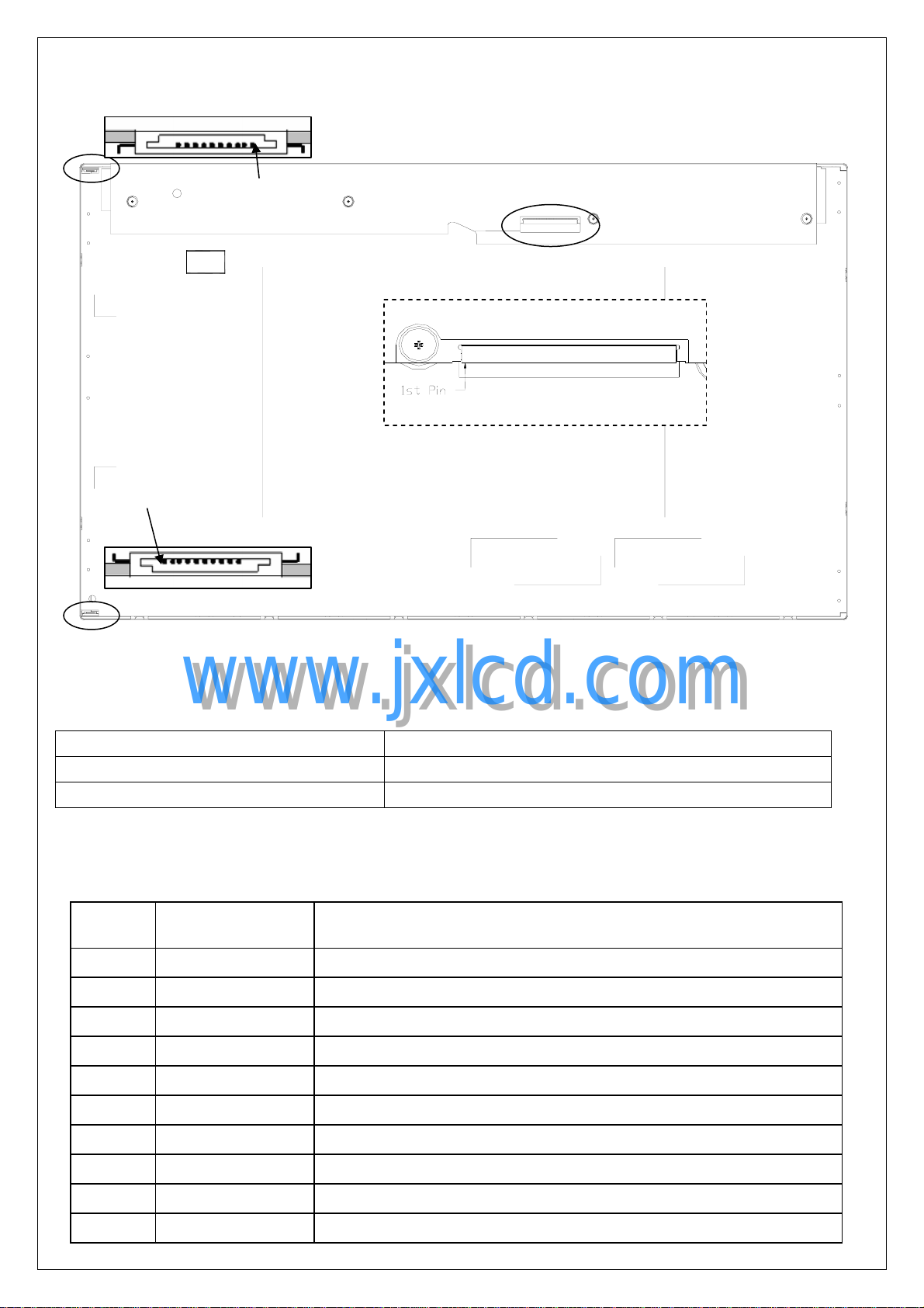
First pin
First pin
SPEC NO.
PAGE
MT230DW01 V.2
7/25
Rear View of LCM
1.2 Recommend Connector for Backlight Unit
This connector is mounted on the monitor system board for LED light-bar FFC mating.
Connector Name/Designation Match Connector
Manufacturer Entery INDUSTRIAL CO.,LTD
Mating type part number 7080-Q10N-00R
1.3 LED Light Bar Connector
Upper Connector Pin Assignment:
Pin No Symbol Description
1 IRLED1 LED current sense for string 1
2 IRLED1 LED current sense for string 1
3 IRLED2 LED current sense for string 2
4 VLED LED power supply
5 VLED LED power supply
www.jxlcd.com
www.jxlcd.com
6 VLED LED power supply
7 VLED LED power supply
8 IRLED2 LED current sense for string 2
9 IRLED3 LED current sense for string 3
10 IRLED3 LED current sense for string 3
Page 7
SPEC NO.
PAGE
Lower Connector Pin Assignment:
Pin No Symbol Description
1 IRLED1 LED current sense for string 1
2 IRLED1 LED current sense for string 1
3 IRLED2 LED current sense for string 2
4 VLED LED power supply
5 VLED LED power supply
6 VLED LED power supply
7 VLED LED power supply
8 IRLED2 LED current sense for string 2
9 IRLED3 LED current sense for string 3
10 IRLED3 LED current sense for string 3
MT230DW01 V.2
8/25
www.jxlcd.com
www.jxlcd.com
Page 8

2. Absolute Maximum Ratings
Parameter Symbol
SPEC NO.
Values
Min. Typ. Max.
PAGE
MT230DW01 V.2
9/25
Unit Remark
Power voltage Vcc
Input signal voltage VLH
Operating temperature Top
Storage temperature TST
Operating Humidity Hop 20 - 90 %RH Note 1
Storage Humidity HST 10 - 90 %RH Note 1
Note 1: The relative humidity must not exceed 90% non-condensing at temperatures of 40°C or less.
At temperatures greater than 40°C, the wet bulb temperature must not exceed 39°C.
Note 2: The unit should not be exposed to corrosive chemicals.
www.jxlcd.com
www.jxlcd.com
-0.3 -
-0.3 -
0 -
-20 -
6.0
4.3
50
60
V
V
°C Note 1
°C Note 2
At 25℃
At 25℃
Page 9

3. Electrical Characteristics
a. Typical operating conditions
Item Symbol Min. Typ. Max. Unit Remark
SPEC NO.
PAGE
MT230DW01 V.2
10/25
Input Voltage
Permissive Power Input Ripple
Black
Input Current
Rush Current
Logic Input
Voltage
LVD S:
IN+, IN-
Note 1: The specified current is under the Vcc =5V, 25 °C, fv=60Hz (frame frequency) condition
whereas black pattern is displayed.
Note 2: The specified current is under the Vcc =5V, 25 °C, fv=60Hz (frame frequency) condition
whereas white pattern is displayed.
Note 3: The specified current is under the Vcc =5V, 25 °C, fv=60Hz (frame frequency) condition
Common Mode Voltage
Differential Input Voltage
Threshold Voltage (High)
Threshold Voltage (Low)
www.jxlcd.com
www.jxlcd.com
White
Mosaic
V
4.5 5 5.5
cc
V
- -
RF
Icc - 1000 -
Icc - 800 -
I
- 950 -
cc
I
- 1.6 3
Rush
VCM - 1.2 -
VID 100 - 600
VTH - - 100
VTL -100 - -
400
V
mVp-p
mA
A Note 4
V
mV
mV Note 5, 6
mV Note 5, 6
Note 1
Note 2
Note 3
whereas mosaic pattern (black & white [8*6]) is displayed.
White: 255 Gray
Black: 0 Gray
Page 10

Note 4: Test condition:
SPEC NO.
PAGE
MT230DW01 V.2
11/25
(1). V
= 5 V, V
DD
rising time = 470 µs ± 10%
DD
(2). Pattern: Mosaic pattern
90%
(3) Test circuit
CONTROL SIGNAL
(HIGH to LOW)
12V
www.jxlcd.com
www.jxlcd.com
Note 5: LVDS signal definition
V
5 V
C3
1uF
DD
R1
47K
R3
47K
Ton=470 μs ± 10%
M1
2SK1059
R2
1K
M2
2SK1399
C2
10000pF
FUSE
VDD (LCD INPUT)
C1
1uF
VIN+ = Positive differential DATA & CLK Input
VIN- = Negative differential DATA & CLK Input
VID = VIN+ – VIN- ,
∆VCM =|VCM
∆VID =|VID
VID+ =|VIH
VID- =|VIL
VCM = (VIN
VCM+ = (VIH
VCM- = (VIL
–VCM-|,
+
–VID-|,
+
–VIH-|,
+
–VIL-|,
+
+VIN-)/2,
+
+VIH-)/2,
+
+VIL-)/2,
+
Page 11

SPEC NO.
PAGE
MT230DW01 V.2
12/25
Note 6: Power on sequence for LCD V
T1
Panel Power
Supply V
DC
90%
10%
90% 90%
Interface
Signals
T2
Backlight Power
Supply
DD
Valid Interface Data
90%
90%
90%
T5
T6
10%
T7
10%
T3 T4
www.jxlcd.com
www.jxlcd.com
Parameter Value Unit
Min Typ. Max ms
T1 0.1 - 10 ms
T2 0 30 50 ms
T3 200 250 - ms
T4 100 250 - ms
T5 0 20 50 ms
T6 0.1 - 10 ms
T7 1000 - - ms
Page 12

SPEC NO.
PAGE
MT230DW01 V.2
13/25
b. Display Color vs. Input Data Signals
The brightness of each primary color (red, green and blue) is based on the 8-bit gray scale data input
for the color; the higher the binary input, the brighter the color. The table below provides a reference for
color versus data input.
Basic
colors
Red
Green
Blue
Color
Black
Red(255)
Green(255)
Blue(255)
Cyan
Magenta
Yellow
White
Red(000) dark
Red(001)
Red(002)
:
Red(253)
Red(254)
Red(255) bright
www.jxlcd.com
www.jxlcd.com
Green(000)dark
Green(001)
Green(002)
:
Green(253)
Green(254)
Green(255)
Blue(000) dark
Blue(001)
Blue(002)
:
Blue(253)
Blue(254)
Blue(255) bright
MSB LSB MSB LSB MSB LSB
R7 R6 R5 R4 R3 R2 R1 R0
0
0
1
1
0
0
0
0
0
0
1
1
1
1
1
1
0
0
0
0
0
0
:
:
1
1
1
1
1
1
0
0
0
0
0
0
:
:
0
0
0
0
bright
0
0
0
0
0
0
0
0
:
:
0
0
0
0
0
0
Red Green Blue
0
0
0
0
0
0
1
1
1
1
1
1
0
0
0
0
0
0
0
0
0
0
0
0
0
0
0
0
0
0
1
1
1
1
1
1
1
1
1
1
1
1
1
1
1
1
1
1
0
0
0
0
0
0
0
0
0
0
0
0
0
:
:
:
1
1
1
1
1
1
1
1
1
1
1
1
0
0
0
0
0
0
0
0
0
0
0
0
:
:
:
0
0
0
0
0
0
0
0
0
0
0
0
0
0
0
0
0
0
0
0
0
0
0
0
:
:
:
0
0
0
0
0
0
0
0
0
0
0
0
0
0
1
1
0
:
:
:
:
:
0
1
1
0
1
1
0
0
0
0
0
0
:
:
0
0
0
0
0
0
0
0
0
0
0
0
:
:
0
0
0
0
0
0
Input color data
G7 G6 G5 G4 G3 G2 G1 G0
0
0
0
0
0
0
0
0
0
0
1
1
1
1
1
0
0
0
0
0
1
1
1
1
1
0
0
0
0
0
1
1
1
1
1
1
1
1
1
1
0
0
0
0
0
0
0
0
0
0
0
0
:
:
:
:
0
0
0
0
0
0
0
0
0
0
0
0
0
0
0
0
0
0
0
0
0
0
0
0
:
:
:
:
1
1
1
1
1
1
1
1
1
1
1
1
0
0
0
0
0
0
0
0
0
0
0
0
:
:
:
:
0
0
0
0
0
0
0
0
0
0
0
0
0
0
0
0
1
1
0
0
1
1
0
0
1
1
1
1
0
0
0
0
0
0
0
0
0
1
1
1
0
0
0
0
0
0
0
0
0
0
0
0
:
:
:
:
:
0
0
0
0
0
0
0
0
0
0
1
0
:
:
0
1
1
1
1
1
0
0
0
0
0
0
:
:
0
0
0
0
0
0
B7 B6 B5 B4 B3 B2 B1 B0
0
0
0
0
0
0
0
0
0
1
0
1
0
1
1
0
0
0
:
0
0
0
0
1
0
:
1
0
1
0
0
0
:
0
0
0
0
0
0
0
1
1
1
1
1
1
1
1
1
0
0
0
1
1
1
0
0
0
0
0
0
0
0
0
:
:
:
0
0
0
0
0
0
0
0
0
0
0
0
0
0
0
0
0
0
:
:
:
0
0
0
0
0
0
0
0
0
0
0
0
0
0
0
0
0
0
:
:
:
1
1
1
1
1
1
1
1
1
0
0
0
0
0
0
0
1
1
1
1
1
1
1
1
1
0
0
0
1
1
1
0
0
0
0
0
0
0
0
0
:
:
:
0
0
0
0
0
0
0
0
0
0
0
0
0
0
0
0
0
0
:
:
:
0
0
0
0
0
0
0
0
0
0
0
0
0
0
0
0
0
0
:
:
:
1
1
1
1
1
1
1
1
1
0
0
0
0
0
0
1
1
1
1
1
1
0
0
1
1
0
0
0
0
0
0
:
:
0
0
0
0
0
0
0
0
0
0
0
0
:
:
0
0
0
0
0
0
0
0
0
1
0
1
:
:
1
0
0
1
1
1
Page 13

c. Input Signal Timing
Support Input Timing Table
Item Description Min. Typ. Max. Unit
SPEC NO.
PAGE
MT230DW01 V.2
14/25
Clock Dclk
T
Vertical
Horizontal
Note: Because this module is operated by DE mode only, Hsync and Vsync input signals should be set to
low Logic level or ground. Otherwise, this module would operate abnormally.
T
T
H_TOTAL
T
V total line number 1090 1100 1160 T
V_TOTAL
Data duration 1080 1080 1080 T
V_DATA
TVB V-blank 10 20 80 T
f
frequency 50 60 75 Hz
V
H total pixel number 1000 1088 1120 DClk
Data duration 960 960 960 DClk
H_DATA
H-blank 40 128 160 DClk
T
HB
INPUT SIGNAL TIMING DIAGRAM
period 11.43 13.89 16.7 nS
frequency 60 72 87.5 MHz
H_TOTAL
H_TOTAL
H_TOTAL
www.jxlcd.com
www.jxlcd.com
Tv
Tvd Tvb
DE
DCLK
Tc
Thb Thd
DE
Page 14

d. Display Position
D(1,1) D(2,1) … … D(960,1) … … D(1919,1) D(1920,1)
D(1,2) D(2,2) … … D(960,2) … … D(1919,2) D(1920,2)
.
.
.
D(1,540) D(2,540) … … D(960,540) … … D(1919,540) D(1920,540)
.
.
.
D(1,1079) D(2,1079) … … D(960,1079) … … D(1919,1079) D(1920,1979)
D(1,1080) D(2,1080) … … D(960,1080) … … D(1919,1080) D(1920,1080)
e. Backlight Unit
SPEC NO.
.
.
.
.
… …
… …
.
.
.
.
.
.
PAGE
… …
… …
MT230DW01 V.2
15/25
.
.
.
.
.
.
.
.
.
.
.
.
Parameter Symbol
Light Bar Input Voltage VLED 39.6 40.8 VDC (Duty 100%)
Light Bar Input Current ILED 360 mADC Note 1, 2, 3
Power Consumption PLED 14.67 W Note 4
LED Life Time LBL --- 30000 --- Hrs Note 5
Note 1: There are two Light Bars, and the specified current is input LED chip 100% duty current.
Note 2: The sensing current of each string is 60mA.
Note 3: Each light bar have three current sensing strings, so that each light bar input current is
180mA.
www.jxlcd.com
www.jxlcd.com
Note 4: PLED = ILED × VLED.
Note 5: The life time is determined as the time at which luminance of the LED becomes 50% of the
initial brightness or not normal lighting at the current I
operating at 25±2°C.
Min. Typ. Max.
Value
Unit Note
=360mA on condition of continuous
LED
Page 15

C. Optical Specifications
SPEC NO.
PAGE
MT230DW01 V.2
16/25
Item Symbol Condition
Tr
Response time
Contrast ratio CR
Viewing angle
Brightness (Center) YL
Tf
Tr+Tf
Top
Bottom
Left
Right
Wx 0.313
Wy 0.329
θ= 0∘
θ= 0∘
CR≧10
CR≧10
CR≧10
CR≧10
Specification
Min. Typ. Max.
- 1.5 3
- 3.5 7
- 5 10
700 1000 -
70 80 -
70 80 -
75 85 -
75 85 -
250 300 -
Unit Remark
ms Note 2
Note 1,3
deg. Note 1,3,5
nit Note 1,4
Rx 0.639
www.jxlcd.com
Color chromaticity(CIE)
White uniformity (9 points)
Note: Ambient temperature = 25°C.
To be measured in dark room after backlight warm up 10 minutes.
Note 1: To be measured with a viewing cone of 2°by Topcon luminance meter BM-5A.
Note 2: Definition of response time:
to “White” (falling time) and from “White” to “Black” (rising time), respectively. The response time
interval is between the 10% and 90% of amplitudes. Refer to figure as below.
www.jxlcd.com
Cross talk Ct
The output signals of BM-7 are measured when the input signals are changed from “Black”
Ry 0.345
Gx 0.324
Gy 0.621
Bx 0.150
By
δW
θ= 0∘
-0.03
0.059
0.7 0.75 -
- - 2%
+0.03
Note 1
Note 1,6
Note 7
Page 16

)
)
SPEC NO.
PAGE
MT230DW01 V.2
17/25
100%
S
i
90%
g
n
a
l
(
R
e
l
a
t
i
v
e
v
a
l
u
10%
e
)
0%
Note 3: Definition of contrast ratio:
Contrast ratio is calculated by the following formula.
Contrast ratio (CR
Note 4: Driving conditions for LED Light Bar: I
Note 5: Definition of viewing angle
Tr
Brightness on the "white" state
=
Brightness on the "black" state
"Black"
=360mA.
LED
"White""White"
Tf
www.jxlcd.com
www.jxlcd.com
Note 6: Definition white uniformity:
Luminance are measured at the following nine points (P1~P9).
δ
Minimum Brightness of nine points(P1~P9
=
Maximum Brightness of nine points (P1~P9)
Page 17

Note 7:
SPEC NO.
1/2
A
127 gray level 127 gray level
1/6
1/6
1/2
B
PAGE
2/3 1/3
A’
1/2
MT230DW01 V.2
18/25
1/6
1/6
1/3
1/2
B’
2/3
www.jxlcd.com
www.jxlcd.com
0 gray level
l L
l L
l / LA x 100%= 2% max., LA and LA’ are brightness at location A and A’
A-LA’
l / LB x 100%= 2% max., LB and LB’ are brightness at location B and B’
B-LB’
Note 10: Optical characteristic measurement setup.
Page 18

D. Reliability Test Items
Test Item Test Condition Judgment Remark
SPEC NO.
PAGE
MT230DW01 V.2
19/24
High temperature storage
Low temperature storage
High temperature & high
humidity operation
High temperature operation
Low temperature operation
Thermal Shock
(non-operation)
Electrostatic discharge (ESD)
(non-operation)
Vibration
(non-operation)
60°C, 240Hrs
-20°C, 240Hrs
40°C, 90%RH, 240Hrs
(No condensation)
50°C, 240Hrs
0°C, 240Hrs
-20°C~60°C
-20°C /1Hr, 60°C /1Hr, 100cycles
Contact:+/-8kV, 150pF(330ohms),
10 times/1 point, 1 time/1 sec, total 16 points
Air discharge:+/-15kV, 150pF(330ohms), 10
times/1 point, 1 time/1 sec, total 9 points
Vibration level : 1.5G
Bandwidth : 10-300Hz
Note 1 Note 2
Note 1 Note 2
Note 1 Note 2
Note 1 Note 2
Note 1 Note 2
Note 1 Note 2
Note 1 Note 2
Note 1 Note 2
Mechanical Shock
(non-operation)
MTBF Demonstration 30,000 hours with confidence level 90% Note 1 Note 3
Note 1: Pass: Normal display image with no obvious non-uniformity and no line defect.
Fail: No display image, obvious non-uniformity, or line defects.
Note 2: Evaluation should be tested after storage at room temperature for two hours.
www.jxlcd.com
www.jxlcd.com
Partial transformation of the module parts should be ignored.
Waveform : sine wave,
sweep rate : 10min
30 min for each direction X, Y, Z
(1.5 Hrs in total)
Shock level : 50G, 11ms
Waveform : Half sine wave
Direction : ±X, ±Y, ±Z
One time each direction
Note 1 Note 2
Note 3: The MTBF calculation is based on the assumption that the failure rate distribution meets the
Exponential Model.
Page 19

E. Safety
(1). Sharp Edge Requirements
There will be no sharp edges or corners on the display assembly that could cause injury.
(2). Materials
a. Toxicity
There will be no carcinogenic materials used anywhere in the display module. If toxic materials are
used, they will be reviewed and approved by the responsible InnoLux Toxicologist.
b. Flammability
All components including electrical components that do not meet the flammability grade UL94-V1 in
the module will complete the flammability rating exception approval process. The printed circuit
board will be made from material rated 94-V1 or better. The actual UL flammability rating will be
printed on the printed circuit board.
c. Capacitors
If any polarized capacitors are used in the display assembly, provisions will be made to keep them
SPEC NO.
PAGE
MT230DW01 V.2
20/24
from being inserted backwards.
F. Display Quality
The display quality of the color TFT-LCD module should be in compliance with the
Innolux’s Incoming inspection standard.
G. Handling Precaution
The Handling of the TFT-LCD should be in compliance with the Innolux’s handling principle
standard.
www.jxlcd.com
www.jxlcd.com
Page 20

H. Label
(1). Module Label
SPEC NO.
73 mm
PAGE
MT230DW01 V.2
21/24
18 mm
(a). Model Number: MT230DW01
(b). Version: V.2
(c). Serial ID I: Z
MT230DW01 V.2 AM2300001 2xx
Z1 Z2 Z3 Z4 Z
Z1 'Z2'-Z3' Z4'Z 5'Z 6'Z7'-Z8' - Z9 '- Z10 '- Z11' Z12'-Z13'-Z14' Z15' -Z16 '-Z17 'Z18' Z19' -Z20'Z21'Z22 ' Z
Z2 Z3 Z4 Z 5 Z 6 Z 7 Z8 Z
1
www.jxlcd.com
www.jxlcd.com
--Z 7--Z8 Z9 Z10 Z
5 Z 6
11 Z 12
MADE IN XXX
9 Z10
'
23
Z
Z
11
12
Serial No
Code of grade
INL internal use
INL internal use
Serial ID includes the information as below:
1. Manufactured Date: Year: 0~9, for 2000~2009
2. Month: 1~9 & A~C for Jan. ~ Dec.
3. Date: 1~9 & A~Z (exclude I, O, Q, U) for 1st~31th
4. Code of grade: 1, 2, 3, 5, E
5. Serial No: Module manufacture sequence no
(d). Serial ID II (INL internal use)
Year, Month, Date
INL internal use
Page 21

(2) Carton Label
SPEC NO.
PAGE
MT230DW01 V.2
22/24
(a). Model Number: MT230DW01
(b). Version: V.2
BOX ID :
60 mm
Model No. MT230DW01 V.2
AM2300001 2XX
Quantity : 7 PCS
MFG Date: 20XX/XX/XX
QC: Made in XXX
INNOLUX DISPLAY
Z1 Z2 Z3 Z4 --Z 5--Z6 Z7 Z8 Z 9
100 mm
(c). Packing quantity: 7 pcs
(d). Serial ID: Z
Serial ID includes the information as below:
(a). Manufactured Date: Year: 0~9, for 2000 ~2009
Month: 1~9 & A~C for Jan. ~ Dec.
Date: 1~9 & A~Z (exclude I, O, Q, U) for 1st~31th
(b). Code of grade: 1, 2, 3, 5, E
(c). Serial No: Module packing sequence no.
Z2 Z3 Z4 Z 5 Z6 Z
www.jxlcd.com
1
www.jxlcd.com
7 Z8
Z 9
Serial No
Code of grade
Year, Month, Date
INL internal use
Page 22

www.jxlcd.com
www.jxlcd.com
Page 23

www.jxlcd.com
www.jxlcd.com
 Loading...