

INNOLUX MT215DW01-VA SPEClFlCATlON

www.jxlcd.com
www.jxlcd.com

www.jxlcd.com
www.jxlcd.com

Record of Revision
Version: 1.0
InnoLux copyright
All rights reserved,
Copying forbidden.
Version Revise Date Pa g e
1.0 2009/11/15
First edition to all Final-Spec.
Content
www.jxlcd.com
www.jxlcd.com

Contents:
SPE C N O.
PAG E
M T 2 15 DW 0 1 V.A
4/24
A. General Specification
B. Electrical Specifications
1. Pin assignment 6
2. Absolute maximum ratings 8
3. Electrical characteristics 9
a. Typical operating conditions 9
b. Display color vs. input data signals 12
c. Inp ut sig nal timin g 13
d. Dis pla y p osition 14
e. Bac kli ght dr iving condit ions 14
5
6
C. Optical specifications
www.jxlcd.com
D. Reliability test items
E. Saf et y
F. Dis play q uality
G. Han dling precaution
H. Lab el
I. Mec hanical dra wings
www.jxlcd.com
16
19
20
20
20
21
23

A. General specification
NO. Item Specification Remark
SPE C N O.
PAG E
M T 2 15 DW 0 1 V.A
5/24
1 Display resolution (pixel)
2 Active area (mm)
3 Screen size (inch)
4 Pixel pitch (mm)
5 Color configuration
6 Overall dimension (mm)
7 Color Gamut
8 Weight (g)
9 Surface treatment
10 Input color signal
11 Display colors
12 Optimum viewing direction
1,920(H) X 1080(V), Full HD resolution
476.64(H) X268.11 (V)
21.53 inches diagonal
0.24825(H) X0.24825 (V)
R, G, B vertical stripe
495.6(W) X 292.2(H) X 16.35 (D) (typ.)
72% NTSC
2200 (Typical)
Anti-Glare, Hard coating (3H)
8 bit LVDS
16.7M (6 bit with Hi-FRC)
6 o’clock
Note 1
13 Backlight
14 Others
Note 1: Glare Option available.
www.jxlcd.com
www.jxlcd.com
4 CCFL
RoHS & Halogen Free compliance
SPE C N O.
PAG E
B. Electrical specifications
1. Pin assignment
Connector
FOXCONN GS23302-0011 R-7F or mechanical interface equivalent connector.
M T 2 15 DW 0 1 V.A
6/24
Pin No
Frame
1 RXinO0- -LVDS differential data input, Chan 0-Odd
2 RXinO0+ +LVDS differential data input, Chan 0-Odd
3 RXinO1- -LVDS differential data input, Chan 1-Odd
4 RXinO1+ +LVDS differential data input, Chan 1-Odd
5 RXinO2- -LVDS differential data input, Chan 2-Odd
6 RXinO2+ +LVDS differential data input, Chan 2-Odd
7 VSS Ground
8 RXOC- -LVDS differential Clock input (Odd)
9 RXOC+ +LVDS differential Clock input (Odd)
10 RXinO3- -LVDS differential data input, Chan 3-Odd
11 RXinO3+ +LVDS differential data input, Chan 3-Odd
12 RXinE0- -LVDS differential data input, Chan 0-Even
13 RXinE0+ +LVDS differential data input, Chan 0-Even
www.jxlcd.com
www.jxlcd.com
14 VSS Ground
Symbol Description
VSS Ground
15 RXinE1- -LVDS differential data input, Chan 1-Even
16 RXinE1+ +LVDS differential data input, Chan 1-Even
17 VSS Ground
18 RXinE2- -LVDS differential data input, Chan 2-Even
19 RXinE2+ +LVDS differential data input, Chan 2-Even
20 RXEC- -LVDS differential Clock input (Even)
21 RXEC+ +LVDS differential Clock input (Even)
22 RXinE3- -LVDS differential data input, Chan 3-Even
23 RXinE3+ +LVDS differential data input, Chan 3-Even
24 VSS Ground
25 NC No Connection
26 NC No Connection
27 NC No Connection
28 VCC +5.0V power supply
29 VCC +5.0V power supply
30 VCC +5.0V power supply
Frame VSS Ground

SPE C N O.
PAG E
M T 2 15 DW 0 1 V.A
7/24
#30
#1
#30
#1
www.jxlcd.com
www.jxlcd.com
#1
Rear view of LCM
#30
CCFL Current
ICFL
[mA]
Note 3
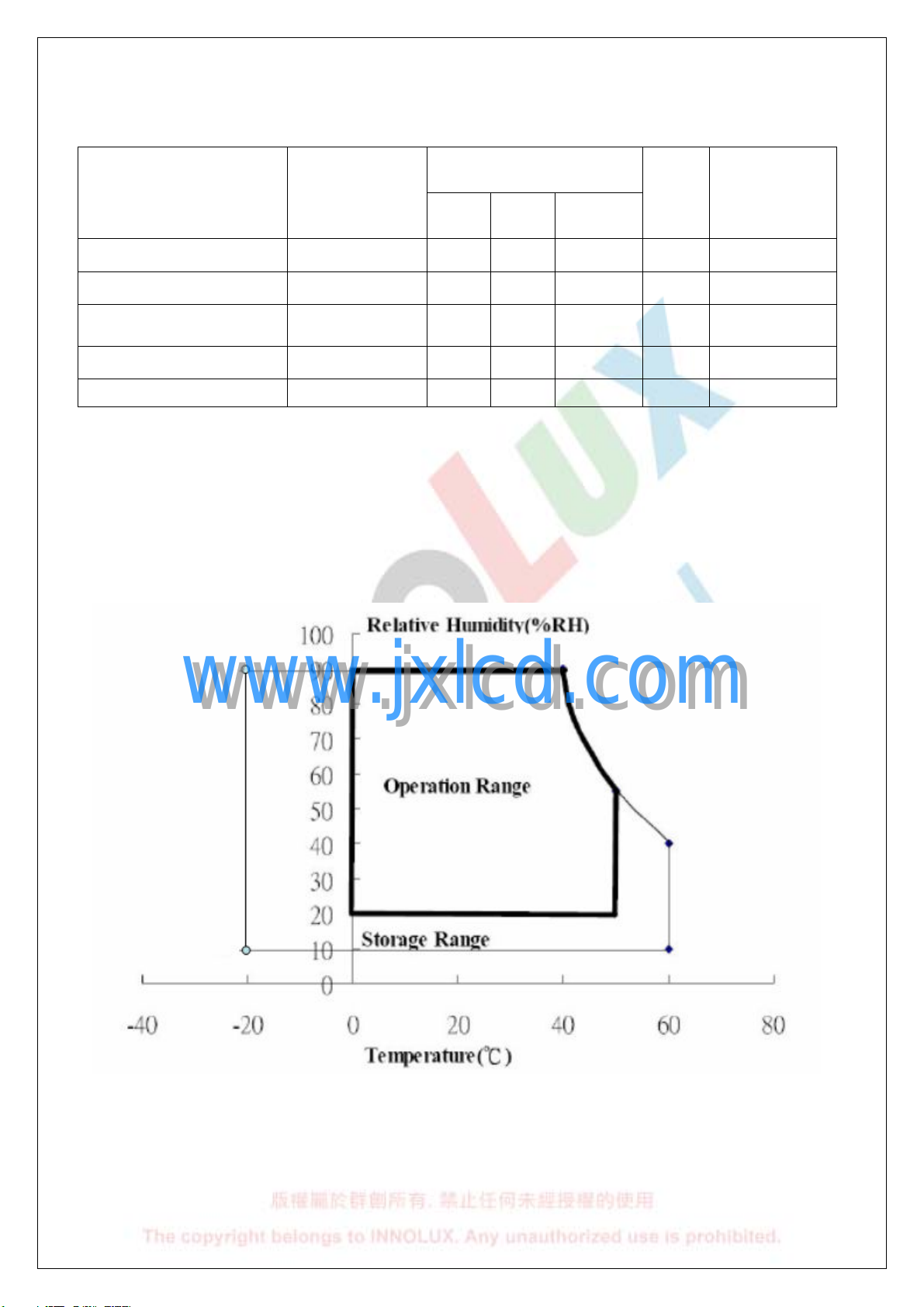
2. Absolute maximum ratings
SPE C N O.
PAG E
M T 2 15 DW 0 1 V.A
8/24
Parameter Symbol
Min.
Power voltage Vcc
Input signal voltage VLH
Operating temperature Top
Storage temperature TST
Note 1: The relative humidity must not exceed 90% non-condensing at temperatures of 40°C or less.
At temperatures greater than 40°C, the wet bulb temperature must not exceed 39°C.
Note 2: The unit should not be exposed to corrosive chemicals.
Note 3: Permanent damage to the device may occur if exceeding maximum values and within 25°C.
-0.3 -
-0.3 -
0 -
-20 -
3.0 - 8.0
Values
Typ.
Max.
6.0 V At 25°C
4.3 V At 25°C
50 °C Note 1
60 °C Note 2
Unit
Remark
www.jxlcd.com
www.jxlcd.com
 Loading...