

Page 1
Global LCD Panel Exchange Center
MODEL NO.: MT190EN02
www.panelook.com
PRODUCT SPECIFICATION
UDoc. Number : MT190EN02 V.W-DR4-26
ϭTentative Specification
ϭPreliminary Specification
ϮApproval Specification
SUFFIX: V.W
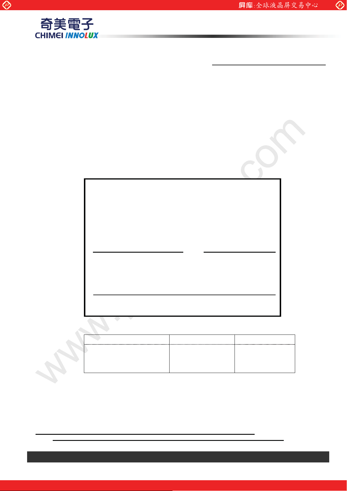
Customer:
APPROVED BY SIGNATURE
Name / Title
Note
Please return 1 copy for your confirmation with your
signature and comments.
Approved By Checked By Prepared By
UMT190EN02 V.W LCD MODULE SPECIFICATION
Version 3.4 17 February 2012 1 / 31
The copyright belongs to CHIMEI InnoLux. Any unauthorized use is prohibited.
One step solution for LCD / PDP / OLED panel application: Datasheet, inventory and accessory!
www.panelook.com
Page 2
Global LCD Panel Exchange Center
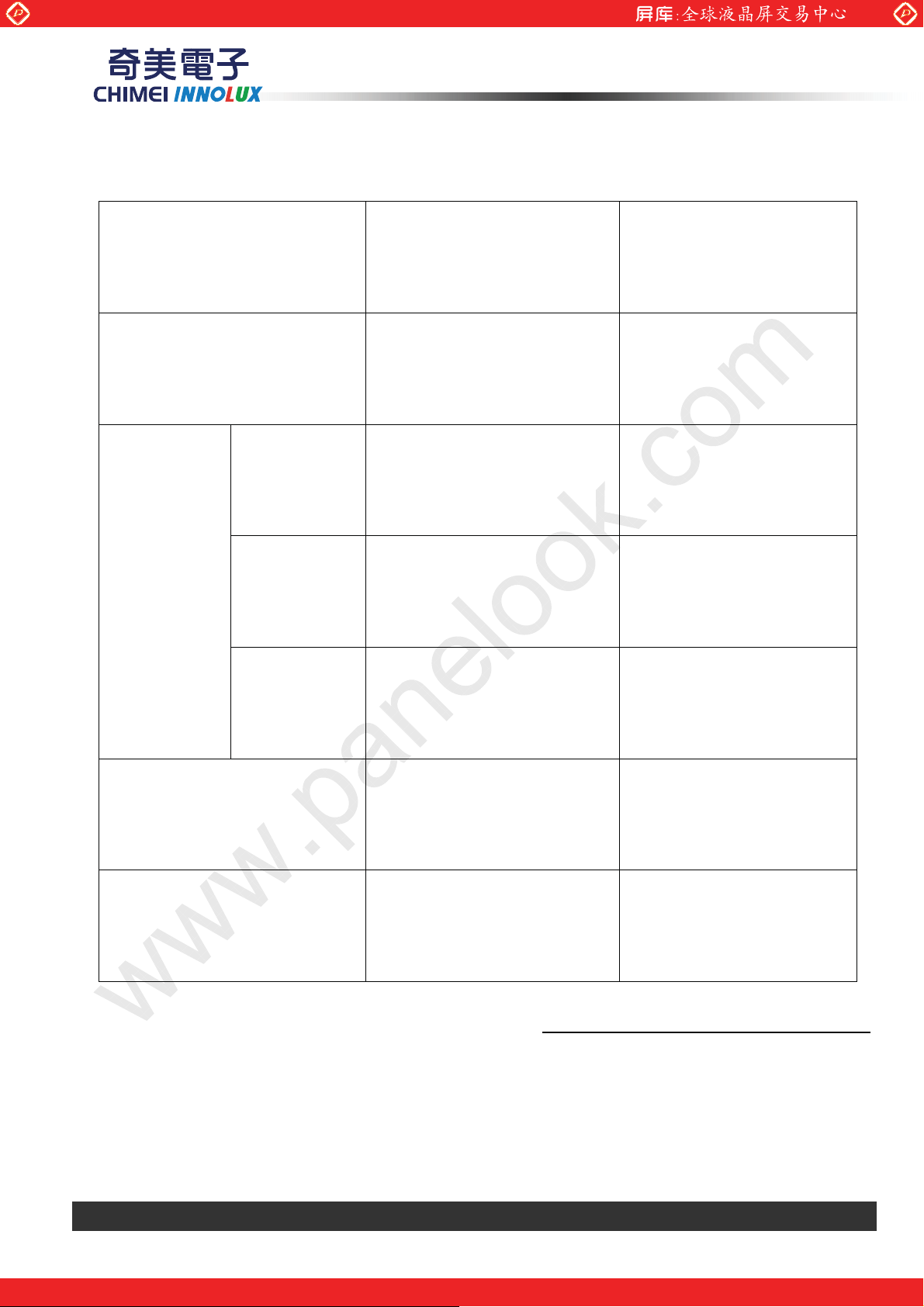
Department Prepared by Checked by
MKT
www.panelook.com
PRODUCT SPECIFICATION
PD
EE
ME
POFA
RA
PE
UDocument Number: MT190EN02 V.W-DR4-26
Version 3.4 17 February 2012 2 / 31
The copyright belongs to CHIMEI InnoLux. Any unauthorized use is prohibited.
One step solution for LCD / PDP / OLED panel application: Datasheet, inventory and accessory!
www.panelook.com
Page 3
Global LCD Panel Exchange Center
www.panelook.com
PRODUCT SPECIFICATION
UCONTENTS
1. GENERAL DESCRIPTION ......................................................................................................7
1.1 OVERVIEW .......................................................................................................................7
1.2 GENERAL SPECIFICATIONS ...........................................................................................7
2. 2. MECHANICAL SPECIFICATIONS ......................................................................................7
3. ABSOLUTE MAXIMUM RATINGS ..........................................................................................7
3.1 ABSOLUTE RATINGS OF ENVIRONMENT ...................................................................... 7
3.2 ELECTRICAL ABSOLUTE RATINGS ................................................................................8
3.2.1 TFT LCD MODULE .................................................................................................... 8
3.2.2 BACKLIGHT UNIT...................................................................................................... 8
4. ELECTRICAL SPECIFICATIONS ............................................................................................9
4.1 FUNCTION BLOCK DIAGRAM .........................................................................................9
4.2. INTERFACE CONNECTIONS .......................................................................................... 9
4.3 ELECTRICAL CHARACTERISTICS................................................................................ 11
4.3.1 LCD ELETRONICS SPECIFICATION .......................................................................11
4.3.2 Vcc Power Dip Condition.......................................................................................... 13
4.3.3 BACKLIGHT UNIT (LED matrix is 10S12P) ............................................................. 13
4.3.4 LIGHTBAR Connector Pin Assignment .................................................................... 14
4.4 LVDS INPUT SIGNAL SPECIFICATIONS ....................................................................... 15
4.4.1 LVDS DATA MAPPING TABLE ................................................................................. 15
4.4.2 COLOR DATA INPUT ASSIGNMENT....................................................................... 15
4.5 DISPLAY TIMING SPECIFICATIONS.............................................................................. 17
4.6 POWER ON/OFF SEQUENCE........................................................................................ 19
5. OPTICAL CHARACTERISTICS ............................................................................................ 20
5.1 TEST CONDITIONS ........................................................................................................ 20
5.2 OPTICAL SPECIFICATIONS ........................................................................................... 20
6. RELIABILITY TEST ITEM.................................................................................................. 23
7. PACKING...............................................................................................................................24
7.1 PACKING SPECIFICATIONS .......................................................................................... 24
7.2 PACKING METHOD ........................................................................................................ 24
7.3 PALLET............................................................................................................................25
8. CMI MODULE LABEL ........................................................................................................... 26
9. PRECAUTIONS .....................................................................................................................28
9.1 ASSEMBLY AND HANDLING PRECAUTIONS ...............................................................28
9.2 STORAGE PRECAUTIONS ............................................................................................28
9.3 OPERATION PRECAUTIONS ......................................................................................... 28
Version 3.4 17 February 2012 3 / 31
The copyright belongs to CHIMEI InnoLux. Any unauthorized use is prohibited.
One step solution for LCD / PDP / OLED panel application: Datasheet, inventory and accessory!
www.panelook.com
Page 4
Global LCD Panel Exchange Center
www.panelook.com
PRODUCT SPECIFICATION
9.4 SAFETY PRECAUTIONS................................................................................................ 28
9.5 SAFETY STANDARDS.................................................................................................... 29
9.6 OTHER ............................................................................................................................29
Appendix. OUTLINE DRAWING............................................................................................... 29
U
Version 3.4 17 February 2012 4 / 31
The copyright belongs to CHIMEI InnoLux. Any unauthorized use is prohibited.
One step solution for LCD / PDP / OLED panel application: Datasheet, inventory and accessory!
www.panelook.com
Page 5
Global LCD Panel Exchange Center
www.panelook.com
REVISION HISTORYU
Record of Revision
Version Revise Page Content
2.0 2010-8-27 All First edition to all Spec.
2.1 2010-10-15 17 The Value of timing specification T1=0.1 update to 0.5
Update altitude test operation:10000ft to 16400ft
21
Non-operation:30000ft to 40000ft,
PRODUCT SPECIFICATION
3.0 2011-5-11 12 Add a drawing about the Lightbar Connector
3.2.2
3.1 2011-12-21 7
To
10 4.3.1 Add Vic Min=1.0,Vin Max=1.4
4.3.3
12
To
5.1
19
3.2 2011-12-27 6
UToU
Add Color Gamut:
72% of NTSC(CIE1931),84% of NTSC(CIE 1976)
4.5 Change Vtotal Max =1150 to Max=1186,
16
Pixel clock Min = 45 to Min=40
V freq Max = 75 to Max=76
4.5 Add Note(4):
3.3 2012-1-5 17
Note (4) The DCLK range at last line of V-blanking should be set in 0 to
Hdisplay/2
18 4.6 Change T6 Max=50 to T6 Max=100
Version 3.4 17 February 2012 5 / 31
The copyright belongs to CHIMEI InnoLux. Any unauthorized use is prohibited.
One step solution for LCD / PDP / OLED panel application: Datasheet, inventory and accessory!
www.panelook.com
Page 6
Global LCD Panel Exchange Center
www.panelook.com
PRODUCT SPECIFICATION
3.4 2012-2-17 13 Update Note Ipin=44mA
30~31 Update 2D Drawing
Version 3.4 17 February 2012 6 / 31
The copyright belongs to CHIMEI InnoLux. Any unauthorized use is prohibited.
One step solution for LCD / PDP / OLED panel application: Datasheet, inventory and accessory!
www.panelook.com
Page 7
Global LCD Panel Exchange Center
www.panelook.com
PRODUCT SPECIFICATION
1. GENERAL DESCRIPTION
1.1 OVERVIEW
MT190EN02 V.W is a 19” TFT Liquid Crystal Display module with WLED Backlight unit and 30 pins 2ch-LVDS
interface. This module supports 1280 x 1024 SXGA mode and can display up to 16.7M colors. The converter
module for Backlight is not built in.
1.2 GENERAL SPECIFICATIONS
Item Specification Unit Note
Screen Size 19 inches diagonal
Driver Element a-si TFT active matrix - -
Pixel Number 1280(H) X 1024(V), SXGA resolution pixel -
Pixel Pitch 0.294(H) X 0.294(V) mm -
Pixel Arrangement R, G, B vertical stripe - -
Display Colors 16.7M (6 bit with Hi-FRC) color -
Transmissive Mode Normally white - -
Surface Treatment Anti-Glare, Haze=25%, Hard coating (3H) - -
Luminance, White 250nits(Typ.) Cd/m2
Color Gamut 72% of NTSC(CIE1931),84%of NTSC(CIE 1976) - -
ROHS,Halogen Free&TCO 5.2 ROHS, Halogen Free TCO 5.2 compliance - -
Power Consumption Total 12.68 W (Max.) @ cell 3.7W (Max.), BL8.98W (Max.) (1)
Note (1) The specified power consumption : Total= cell (reference 4.3.1)+BL (reference 4.3.3)
2. 2. MECHANICAL SPECIFICATIONS
Item Min. Typ. Max. Unit Note
Module
Size
Bezel Area
Active Area
Note (1) Please refer to the attached drawings for more information of front and back outline dimensions.
Horizontal (H) U395.5U U396U U396.5U mm
Vertical (V) U323.5U U324U U324.5U mm
Thickness (T) --Horizontal 380 380.3 380.6 mm
Vertical 304.7 305 305.3 mm
Horizontal --- 376.32 --- mm
Vertical --- 301.06 --- mm
Weight --- U1400U U1500U g
U10.5U U11U mm
3. ABSOLUTE MAXIMUM RATINGS
3.1 ABSOLUTE RATINGS OF ENVIRONMENT
Item Symbol
Min. Max.
Storage Temperature TST -20 60 ºC (1)
Operating Ambient Temperature TOP 0 50 ºC (1), (2)
Value
Unit Note
(1)
Note (1)
(a) 90 %RH Max. (Ta <= 40 ºC).
(b) Wet-bulb temperature should be 39 ºC Max. (Ta > 40 ºC).
Version 3.4 17 February 2012 7 / 31
The copyright belongs to CHIMEI InnoLux. Any unauthorized use is prohibited.
One step solution for LCD / PDP / OLED panel application: Datasheet, inventory and accessory!
www.panelook.com
Page 8
Global LCD Panel Exchange Center
www.panelook.com
PRODUCT SPECIFICATION
(c) No condensation.
Note (2) The temperature of panel surface should be 0 ºC min. and 60 ºC max.
3.2 ELECTRICAL ABSOLUTE RATINGS
3.2.1 TFT LCD MODULE
Item Symbol
Power Supply Voltage VCCS -0.3 6.0 V
Logic Input Voltage VB
B -0.3 2.8 V
IN
Value
Min. Max.
Unit Note
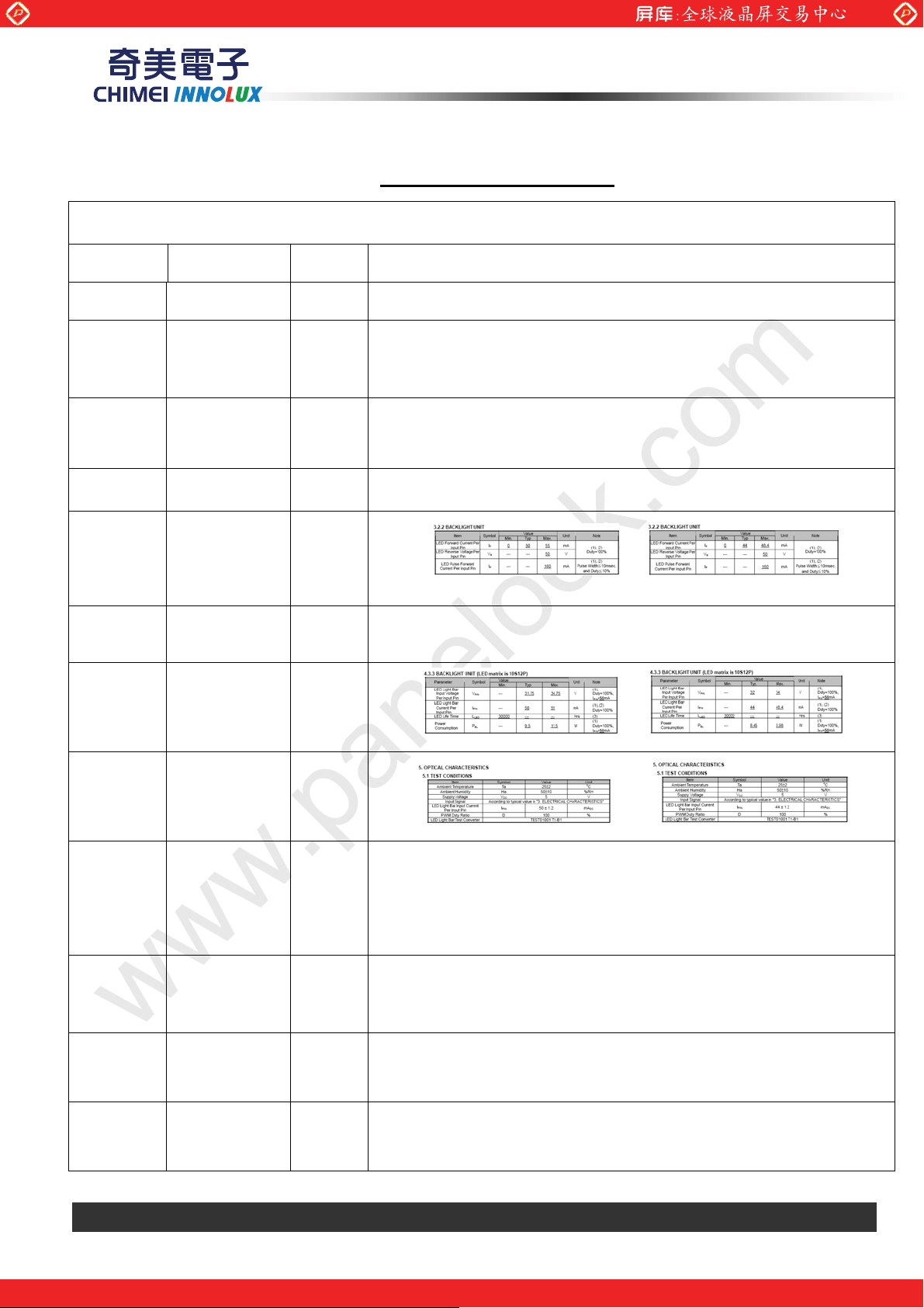
3.2.2 BACKLIGHT UNIT
Item Symbol
LED Forward Current Per
input Pin
LED Reverse Voltage Per
Input Pin
LED Pulse Forward
Current Per input Pin
B
B U0U U44U U48.4U mA
I
F
B
B --- --- U50U V
V
R
B
B --- --- U160U mA
I
P
Min. Typ Max.
Note (1) Permanent damage to the device may occur if maximum values are exceeded. Function operation
should be restricted to the conditions described under Normal Operating Conditions.
Value
Unit Note
(1), (2)
Duty=100%
(1), (2)
Pulse WidthЉ10msec.
and DutyЉ10%
(1)
Note (2) Specified values are for input pin of LED light bar at Ta=25±2°C (Refer to 4.3.3 and 4.3.4 for further
information).
Version 3.4 17 February 2012 8 / 31
The copyright belongs to CHIMEI InnoLux. Any unauthorized use is prohibited.
One step solution for LCD / PDP / OLED panel application: Datasheet, inventory and accessory!
www.panelook.com
Page 9
Global LCD Panel Exchange Center
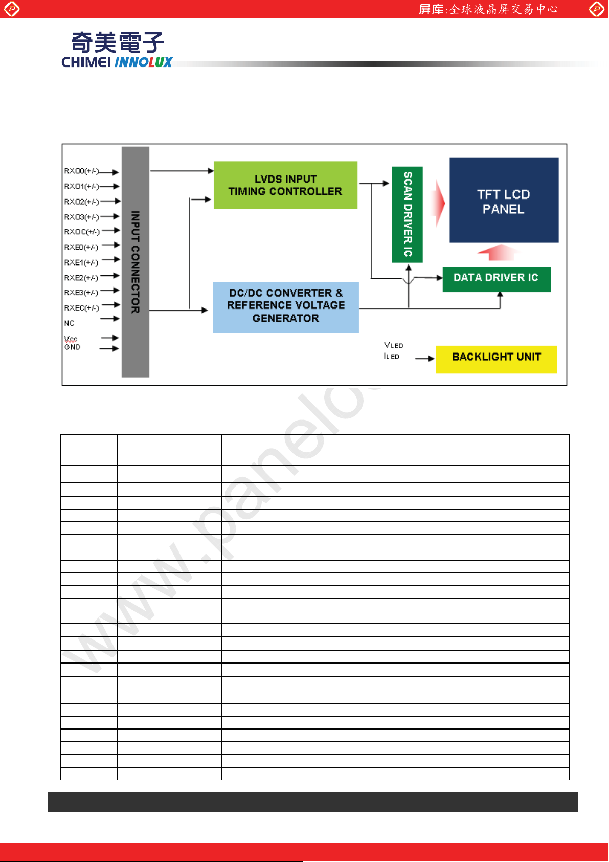
4. ELECTRICAL SPECIFICATIONS
4.1 FUNCTION BLOCK DIAGRAM
www.panelook.com
PRODUCT SPECIFICATION
4.2. INTERFACE CONNECTIONS
PIN ASSIGNMENT
Pin No Symbol Description
Frame VSS Ground
1 RXinO0- -LVDS differential data input, Chan 0-Odd
2 RXinO0+ +LVDS differential data input, Chan 0-Odd
3 RXinO1- -LVDS differential data input, Chan 1-Odd
4 RXinO1+ +LVDS differential data input, Chan 1-Odd
5 RXinO2- -LVDS differential data input, Chan 2-Odd
6 RXinO2+ +LVDS differential data input, Chan 2-Odd
7 VSS Ground
8 RXOC- -LVDS differential Clock input (Odd)
9 RXOC+ +LVDS differential Clock input (Odd)
10 RXinO3- -LVDS differential data input, Chan 3-Odd
11 RXinO3+ +LVDS differential data input, Chan 3-Odd
12 RXinE0- -LVDS differential data input, Chan 0-Even
13
14 VSS Ground
15 RXinE1- -LVDS differential data input, Chan 1-Even
16 RXinE1+ +LVDS differential data input, Chan 1-Even
17
18 RXinE2- -LVDS differential data input, Chan 2-Even
19 RXinE2+ +LVDS differential data input, Chan 2-Even
20 RXEC- -LVDS differential Clock input (Even)
21 RXEC+ +LVDS differential Clock input (Even)
22
23 RXinE3+ +LVDS differential data input, Chan 3-Even
RXinE0+ +LVDS differential data input, Chan 0-Even
VSS Ground
RXinE3- -LVDS differential data input, Chan 3-Even
Version 3.4 17 February 2012 9 / 31
The copyright belongs to CHIMEI InnoLux. Any unauthorized use is prohibited.
One step solution for LCD / PDP / OLED panel application: Datasheet, inventory and accessory!
www.panelook.com
Page 10
Global LCD Panel Exchange Center
24 VSS Ground
25 NC No Connection
26 NC No Connection
27 NC No Connection
28
29 VCC +5.0V power supply
30
Frame
Note (1) Connector Part No.:
GS23302-0311R-7H (Foxconn) or 187007-30091 (P-TWO) or equivalent
Note (2) The first pixel is odd.
Note (3) Input signal of even and odd clock should be the same timing.
VCC +5.0V power supply
VCC +5.0V power supply
VSS Ground
www.panelook.com
PRODUCT SPECIFICATION
1,1
(odd)
2,1
3,1
1,2
(even)
2,2
1,3
(odd)
1,4
(even)
1,Xmax
Pitch
Pitch
Ymax,1
Version 3.4 17 February 2012 10 / 31
The copyright belongs to CHIMEI InnoLux. Any unauthorized use is prohibited.
One step solution for LCD / PDP / OLED panel application: Datasheet, inventory and accessory!
Ymax,
Xmax
www.panelook.com
Page 11

Global LCD Panel Exchange Center
V
V
P
4.3 ELECTRICAL CHARACTERISTICS
4.3.1 LCD ELETRONICS SPECIFICATION
Parameter Symbol
Power Supply Voltage Vcc 4.5 5 5.5 V -
Ripple Voltage VB
Rush Current IB
Power Supply Current
Vertical Stripe
Power Consumption PLCD -- -- 3.7 Watt (4)
LVDS differential input voltage Vid 100 -- 600 mV
LVDS common input voltage Vic 1.0 1.2 1.4 V
Logic High Input Voltage VIH -- -- 100 mV
Logic Low Input Voltage VIL -100 -- -- mV
Note (1) The ambient temperature is Ta = 25 ± 2 ºC.
www.panelook.com
PRODUCT SPECIFICATION
Value
Min. Typ. Max.
B -- -- 150 mV -
RP
B -- 1.6 3 A (2)
RUSH
White -- 500 700 mA (3)a
Black -- 700 1000 mA (3)b
Icc
-- 700 1000 mA (3)c
Unit Note
Note (2) Measurement Conditions:
(High to Low)
(Control Signal)
+
+
UVcc rising time is 470
2SK1475
2SK1470
0.01uF
s±10%
FUS
(LCD Module Input)
1
Vcc
0.9Vcc
0.1Vcc
GND
Version 3.4 17 February 2012 11 / 31
The copyright belongs to CHIMEI InnoLux. Any unauthorized use is prohibited.
One step solution for LCD / PDP / OLED panel application: Datasheet, inventory and accessory!
www.panelook.com
Page 12

Global LCD Panel Exchange Center
Note (3) The specified power supply current is under the conditions at Vcc = 5.0 V, Ta = 25 ± 2 ºC,
Fr = 60Hz, whereas a power dissipation check pattern below is displayed.
www.panelook.com
PRODUCT SPECIFICATION
Note (4) The power consumption is specified at the pattern with the maximum current.
Note (5) VID waveform condition
Version 3.4 17 February 2012 12 / 31
The copyright belongs to CHIMEI InnoLux. Any unauthorized use is prohibited.
One step solution for LCD / PDP / OLED panel application: Datasheet, inventory and accessory!
www.panelook.com
Page 13

Global LCD Panel Exchange Center
4.3.2 Vcc Power Dip Condition
www.panelook.com
PRODUCT SPECIFICATION
4.0V
Td
4.3.3 BACKLIGHT UNIT (LED matrix is 10S12P)
Parameter Symbol
LED Light Bar
Input Voltage
Per Input Pin
LED Light Bar
Current Per
Input Pin
LED Life Time LB
Power
Consumption
B
B --- U32U U34U V
V
PIN
B
B --- U44U U48.4U mA
I
PIN
B U30000U U---U U---U Hrs (3)
LED
B
B --- U8.45U U8.98U W
P
BL
Min. Typ. Max.
Value
4.5V
Vcc
Unit Note
(1),
Duty=100%,
B
B=U44UmA
I
PIN
(1), (2)
Duty=100%
(1)
Duty=100%,
B
B=U44UmA
I
PIN
Note (1) LED light bar input voltage and current are measured by utilizing a true RMS multimeter as shown
below:
UNote (2) PUBUBLUBU = VUBU
PIN
UBU ×IUBU
UBU × ( 6 ) Feedback pins , LED light bar circuit is (10)Series, (12)Parallel.
PIN
Note (3) The lifetime of LED is defined as the time when LED packages continue to operate under the
conditions at Ta = 25 ±2 кand I= (
U22)mA (per chip) until the brightness becomes Љ50% of its
original value.
Light bar
IRLED
IRLED
ʳ
IRLED
ʳ
VLED
Connector
VLED
VLED
VLED
IRLED
ʳ
IRLED
ʳ
IRLED
ʳ
VLED
Version 3.4 17 February 2012 13 / 31
The copyright belongs to CHIMEI InnoLux. Any unauthorized use is prohibited.
One step solution for LCD / PDP / OLED panel application: Datasheet, inventory and accessory!
www.panelook.com
Page 14

Global LCD Panel Exchange Center
4.3.4 LIGHTBAR Connector Pin Assignment
UConnector: 7083K-F10N-01L (Entery) / FF04-404-103A (FCN) or Compatible
www.panelook.com
PRODUCT SPECIFICATION
CN1
Pin number Description
1
2
3
4
5
6
7
8
9
10
LED current sense for string 6
LED current sense for string 5
LED current sense for string 4
LED power supply
LED power supply
LED power supply
LED power supply
LED current sense for string 3
LED current sense for string 2
LED current sense for string 1
Version 3.4 17 February 2012 14 / 31
The copyright belongs to CHIMEI InnoLux. Any unauthorized use is prohibited.
One step solution for LCD / PDP / OLED panel application: Datasheet, inventory and accessory!
www.panelook.com
Page 15

Global LCD Panel Exchange Center
4.4 LVDS INPUT SIGNAL SPECIFICATIONS
Pin 1
www.panelook.com
PRODUCT SPECIFICATION
Pin 1
4.4.1 LVDS DATA MAPPING TABLE
LVDS Channel O0
LVDS Channel O1
LVDS Channel O2
LVDS Channel O3
LVDS Channel E0
LVDS Channel E1
LVDS Channel E2
LVDS Channel E3
LVDS output D7 D6 D4 D3 D2 D1 D0
Data order OG0 OR5 OR4 OR3 OR2 OR1 OR0
LVDS output D18 D15 D14 D13 D12 D9 D8
Data order OB1 OB0 OG5 OG4 OG3 OG2 OG1
LVDS output D26 D25 D24 D22 D21 D20 D19
Data order DE NA NA OB5 OB4 OB3 OB2
LVDS output D23 D17 D16 D11 D10 D5 D27
Data order NA OB7 OB6 OG7 OG6 OR7 OR6
LVDS output D7 D6 D4 D3 D2 D1 D0
Data order EG0 ER5 ER4 ER3 ER2 ER1 ER0
LVDS output D18 D15 D14 D13 D12 D9 D8
Data order EB1 EB0 EG5 EG4 EG3 EG2 EG1
LVDS output D26 D25 D24 D22 D21 D20 D19
Data order DE NA NA EB5 EB4 EB3 EB2
LVDS output D23 D17 D16 D11 D10 D5 D27
Data order NA EB7 EB6 EG7 EG6 ER7 ER6
4.4.2 COLOR DATA INPUT ASSIGNMENT
The brightness of each primary color (red, green and blue) is based on the 8-bit gray scale data input for the
color. The higher the binary input, the brighter the color. The table below provides the assignment of color
versus data input.
Note (1) 0: Low Level Voltage, 1: High Level Voltage
Version 3.4 17 February 2012 15 / 31
The copyright belongs to CHIMEI InnoLux. Any unauthorized use is prohibited.
One step solution for LCD / PDP / OLED panel application: Datasheet, inventory and accessory!
www.panelook.com
Page 16

Global LCD Panel Exchange Center
www.panelook.com
PRODUCT SPECIFICATION
Input color data
Basic
colors
Red
Green
Color
Black
Red(255)
Green(255)
Blue(255)
Cyan
Magenta
Yellow
White
Red(000) dark
Red(001)
Red(002)
:
Red(253)
Red(254)
Red(255) bright
Green(000)dark
Green(001)
G
reen(002)
:
Green(253)
Green(254)
Green(255)
bright
Red Green Blue
MSB LSB MSB LSB MSB LSB
R7 R6 R5 R4 R3 R2 R1 R0
0
0
0
0
0
0
0
1
1
1
1
1
1
1
0
0
0
0
0
0
0
0
0
0
0
0
0
0
0
0
0
0
0
0
0
1
1
1
1
1
1
1
1
1
1
1
1
1
1
1
1
1
1
1
1
1
0
0
0
0
0
0
0
0
0
0
0
0
0
0
0
:
:
:
:
1
1
1
1
1
1
1
1
1
1
1
1
1
1
1
0
0
0
0
0
0
0
0
:
:
0
0
0
0
0
0
0
0
0
0
0
0
0
:
:
0
0
0
0
0
0
0
0
0
0
0
0
0
1
0
:
:
:
:
0
1
1
1
1
1
0
0
0
0
0
0
:
:
0
0
0
0
0
0
G7 G6 G5 G4 G3 G2 G1 G0
0
0
0
0
0
0
0
0
1
1
0
0
0
1
0
0
1
1
1
1
1
0
1
0
:
1
0
1
0
0
0
:
0
0
0
0
1
1
0
0
1
1
0
0
1
1
1
1
0
0
0
0
0
0
0
0
0
:
:
:
0
0
0
0
0
0
0
0
0
0
0
0
0
0
0
0
0
0
:
:
:
1
1
1
1
1
1
1
1
1
0
0
0
0
1
1
1
0
0
0
1
1
1
0
0
0
1
1
1
1
1
1
0
0
0
0
0
0
0
0
0
:
:
:
0
0
0
0
0
0
0
0
0
0
0
0
0
0
0
0
0
0
:
:
:
1
1
1
1
1
1
1
1
1
B7 B6 B5 B4 B3 B2 B1 B0
0
0
0
0
0
0
0
0
0
1
1
1
0
0
1
1
1
1
0
0
0
1
1
1
1
1
0
0
0
0
0
0
0
0
0
:
:
:
0
0
0
0
0
0
0
0
0
0
0
0
0
1
0
1
0
0
:
:
:
0
1
0
1
0
0
1
1
0
0
0
0
0
0
0
0
1
1
1
1
1
1
1
1
1
0
0
0
1
1
1
0
0
0
0
0
0
0
0
0
:
:
:
0
0
0
0
0
0
0
0
0
0
0
0
0
0
0
0
0
0
:
:
:
0
0
0
0
0
0
0
0
0
0
0
0
0
0
0
0
0
0
0
0
0
1
1
1
1
1
1
1
1
1
1
1
1
0
0
0
0
1
1
1
1
0
0
0
0
0
0
0
0
0
:
:
:
0
0
0
0
0
0
0
0
0
0
0
0
0
0
0
0
0
0
:
:
:
0
0
0
0
0
0
0
0
0
0
0
0
:
0
0
0
0
0
0
:
0
0
0
0
Blue(000) dark
Blue(001)
Blue(002)
Blue
Blue(253)
Blue(254)
Blue(255) bright
0
0
0
0
0
0
0
0
0
0
0
0
0
0
0
:
:
:
:
:
0
0
0
0
0
0
0
0
0
0
0
0
0
0
0
0
0
0
0
0
0
:
:
0
0
0
0
0
0
0
0
0
0
0
0
0
0
:
:
:
:
0
0
0
0
0
0
0
0
0
0
0
0
0
0
0
0
0
0
:
:
0
0
0
0
0
0
0
0
0
0
0
0
0
:
0
0
0
0
0
0
0
0
0
0
0
0
0
0
0
0
0
0
0
0
0
0
0
0
0
0
0
0
:
:
:
:
:
:
:
:
0
0
1
1
1
1
1
1
0
0
1
1
1
1
1
1
0
0
1
1
1
1
1
1
1
0
0
1
:
:
:
1
0
0
1
1
1
Version 3.4 17 February 2012 16 / 31
The copyright belongs to CHIMEI InnoLux. Any unauthorized use is prohibited.
One step solution for LCD / PDP / OLED panel application: Datasheet, inventory and accessory!
www.panelook.com
Page 17

Global LCD Panel Exchange Center
4.5 DISPLAY TIMING SPECIFICATIONS
The input signal timing specifications are shown as the following table and timing diagram.
Signal Item Symbol Min. Typ. Max. Unit Note
LVDS Clock
Vertical Display Term
Horizontal Display Term
Note: Because this module is operated by DE only mode, Hsync and Vsync input signals should be set to
www.panelook.com
PRODUCT SPECIFICATION
Frequency Fc 40 54 68 MHz -
Period Tc 14.71 18.52 22.22 ns
Input cycle to
cycle jitter
Input Clock
to data skew
Spread
spectrum
modulation
range
Spread
spectrum
modulation
frequency
Frame Rate Fr 50 60 76 Hz Tv=Tvd+Tvb
Total Tv 1044 1066 1186 Th -
Active
Display
Blank Tvb 20 42 -- Th -
Total Th 790 844 880 Tc Th=Thd+Thb
Active
Display
Blank Thb 150 204 -- Tc -
B
B
T
rcl
TLVCCS
Fclkin_
mod
-0.02*TB
TB
-0.02*
0.97*FC
--
B
C
B
C
--
--
0.02*TB
0.02*TB
1.03*FC
ns (1)
B
C
(2)
B
C
MHz
(3)
B
B -- -- 100 KHz
F
SSM
Tvd -- 1024 -- Th -
Thd -- 640 -- Tc -
low Logic level or ground. Otherwise, this module would operate abnormally.
INPUT SIGNAL TIMING DIAGRAM
Version 3.4 17 February 2012 17 / 31
The copyright belongs to CHIMEI InnoLux. Any unauthorized use is prohibited.
One step solution for LCD / PDP / OLED panel application: Datasheet, inventory and accessory!
www.panelook.com
Page 18

Global LCD Panel Exchange Center
www.panelook.com
PRODUCT SPECIFICATION
Note (1) The input clock cycle-to-cycle jitter is defined as below figures. Trcl = I TB
Note (2) Input Clock to data skew is defined as below figures.
B – TI
1
Note (3) The SSCG (Spread spectrum clock generator) is defined as below figures.
Note (4) The DCLK range at last line of V-blanking should be set in 0 to Hdisplay/2.
Version 3.4 17 February 2012 18 / 31
The copyright belongs to CHIMEI InnoLux. Any unauthorized use is prohibited.
One step solution for LCD / PDP / OLED panel application: Datasheet, inventory and accessory!
www.panelook.com
Page 19

Global LCD Panel Exchange Center
4.6 POWER ON/OFF SEQUENCE
The power sequence specifications are shown as the following table and diagram.
www.panelook.com
PRODUCT SPECIFICATION
Timing Specifications:
Parameters
T1 0.5 -- 10 ms
T2 0 30 50 ms
T3 200 250 -- ms
T4 100 250 --- ms
T5 0 20 50 ms
T6 0.1 -- 100 ms
T7 1000 -- -- ms
Note (1) The supply voltage of the external system for the module input should be the same as the definition
of Vcc.
Note (2) When the backlight turns on before the LCD operation of the LCD turns off, the display may
momentarily become abnormal screen.
Note (3) In case of VCC = off level, please keep the level of input signals on the low or keep a high
impedance.
Note (4) T4 should be measured after the module has been fully discharged between power off and on
period.
Min Typ. Max
Valu es
Units
Note (5) Interface signal shall not be kept at high impedance when the power is on.
Version 3.4 17 February 2012 19 / 31
The copyright belongs to CHIMEI InnoLux. Any unauthorized use is prohibited.
One step solution for LCD / PDP / OLED panel application: Datasheet, inventory and accessory!
www.panelook.com
Page 20

Global LCD Panel Exchange Center
Note (6) CMI won’t take any responsibility for the products which are damaged by the customers not
following the Power Sequence.
Note (7) There might be slight electronic noise when LCD is turned off (even backlight unit is also off). To
avoid this symptom, we suggest "Vcc falling timing" to follow "t6 spec".
5. OPTICAL CHARACTERISTICS
5.1 TEST CONDITIONS
Item Symbol Value Unit
Ambient Temperature Ta
Ambient Humidity Ha
Supply Voltage VB
Input Signal According to typical value in "3. ELECTRICAL CHARACTERISTICS"
LED Light Bar Input Current
Per Input Pin
PWM Duty Ratio D 100 %
LED Light Bar Test Converter TEST01001 T1-B1
www.panelook.com
PRODUCT SPECIFICATION
PoP
25r2
50r10
B 5 V
CC
B
B 44 ± 1.2 mAB
I
PIN
C
%RH
DC
B
5.2 OPTICAL SPECIFICATIONS
The relative measurement methods of optical characteristics are shown in 5.2. The following items should be
measured under the test conditions described in 5.1 and stable environment shown in Note (5).
Item Symbol Condition Min. Typ. Max. Unit Note
Red
Color
Green
Chromaticity
(CIE 1931)
Blue
White
Center Luminance of White
(Center of Screen)
Contrast Ratio CR
Response Time
White uniformity
Horizontal
Viewing Angle
Vertical
Horizontal
Viewing Angle
Vertical
Rx 0.636
Ry 0.347
Gx 0.312
Gy 0.622
Bx 0.148
T
B
B=0q, TBYB =0q
By 0.053
x
Typ –
0.03
Typ +
0.03
- (1), (5)
Wx 0.313
Wy
B
B 200 250 --- cd/mP
L
C
0.329
2
P
700 1000 --- - (2), (5)
TB
B --- 1.5 4
R
BFB
T
GW T
Γ x- + Γ
x+
Γ y- + Γ
y+
Γ x- + Γ
x+
Γ y- + Γ
y+
TB
B=0q, TBYB =0q
x
B
B=0q, TBYB =0q
x
CRЊ10
CRЊ5
--- 3.5 6
0.75 --- --- - (5), (6)
150 170
140 160
160 178
150 170
----
----
---
---
ms (3)
Deg. (1), (5)
Deg. (1), (5)
(4), (5)
Version 3.4 17 February 2012 20 / 31
The copyright belongs to CHIMEI InnoLux. Any unauthorized use is prohibited.
One step solution for LCD / PDP / OLED panel application: Datasheet, inventory and accessory!
www.panelook.com
Page 21

Global LCD Panel Exchange Center
Note (1) Definition of Viewing Angle (Tx, Ty):
www.panelook.com
PRODUCT SPECIFICATION
Note (2) Definition of Contrast Ratio (CR):
The contrast ratio can be calculated by the following expression.
Contrast Ratio (CR) = L255 / L0
L255: Luminance of gray level 255
L 0: Luminance of gray level 0
CR = CR (5)
CR (X) is corresponding to the Contrast Ratio of the point X at Figure in Note (6).
Note (3) Definition of Response Time (T
B
R
B, TBFB):
Version 3.4 17 February 2012 21 / 31
The copyright belongs to CHIMEI InnoLux. Any unauthorized use is prohibited.
One step solution for LCD / PDP / OLED panel application: Datasheet, inventory and accessory!
www.panelook.com
Page 22

Global LCD Panel Exchange Center
www.panelook.com
PRODUCT SPECIFICATION
Note (4) Definition of Luminance of White (LB
B):
C
Measure the luminance of gray level 255 at center point
LB
B = L (5)
C
L (x) is corresponding to the luminance of the point X at Figure in Note (6).
Note (5) Measurement Setup:
The LCD module should be stabilized at given temperature for 10 minutes to avoid abrupt
temperature change during measuring. In order to stabilize the luminance, the measurement should
be executed after lighting Backlight for 10 minutes in a windless room.
Back-Light ON Condition
Measuring Instrument:TOPCON BM-5A,SR-3A
Field:2°
500 mm
500 mm
B
Note (6) Definition of White Variation (GW):
Measure the luminance of gray level 255 at 9 points
GW = Minimum [L (1) ~ L (9)] / Maximum [L (1) ~ L (9)]
Center of the screen
Center of the screen
LCD Module
LCD Module
Version 3.4 17 February 2012 22 / 31
The copyright belongs to CHIMEI InnoLux. Any unauthorized use is prohibited.
One step solution for LCD / PDP / OLED panel application: Datasheet, inventory and accessory!
www.panelook.com
Page 23

Global LCD Panel Exchange Center
6. RELIABILITY TEST ITEM
Items Required Condition Note
Temperature Humidity Bias (THB) 50°C , 80%RH, 240hours
High Temperature Operation
(HTO) 50°C, 240Hrs
Low Temperature Operation
(LTO)
High Temperature Storage (HTS) 60°C, 240Hrs
Low Temperature Storage (LTS) -20°C, 240Hrs
Vibration Test
(Non-operation)
Shock Test
(Non-operation)
Thermal Shock Test (TST)
On/Off Test
ESD (Electro Static Discharge)
Altitude Test
Note (1) criteria : Normal display image with no obvious non-uniformity and no line defect.
www.panelook.com
PRODUCT SPECIFICATION
0°C, 240Hrs
Acceleration: 1.5 Grms
Wave: Half-sine
Frequency: 10 - 300 Hz
Sweep: 30 Minutes each Axis (X, Y, Z)
Acceleration: 50 G
Wave: Half-sine
Active Time: 11 ms
Direction : ± X, ± Y, ± Z.(one time for
each Axis)
-20°C~60°C
1Hr, 1Hr, 100cycles
25°C ,On/10sec , Off /10sec , 30,000
cycles
Contact Discharge: ± 8KV,
150pF(330)
Air Discharge: ± 15KV, 150pF(330)
Operation:16,400 ft / 24hours
Non-Operation:40,000 ft / 12 hours
Note (2) Evaluation should be tested after storage at room temperature for more than two hour
Note (3) At testing Vibration and Shock, the fixture in holding the module has to be hard and rigid enough so
that the module would not be twisted or bent by the fixture.
The fixing condition is shown as below:
Version 3.4 17 February 2012 23 / 31
The copyright belongs to CHIMEI InnoLux. Any unauthorized use is prohibited.
One step solution for LCD / PDP / OLED panel application: Datasheet, inventory and accessory!
www.panelook.com
Page 24

Global LCD Panel Exchange Center
7. PACKING
7.1 PACKING SPECIFICATIONS
(1) 9 LCD modules / 1 Box
(2) Box dimensions: 470(L) X 282(W) X 442(H) mm
(3) Weight: approximately: 15.13Kg (9 modules per box)
7.2 PACKING METHOD
(1) Carton Packing should have no failure in the following reliability test items.
Test Item Test Conditions Note
Vibration
Dropping Test 1 Corner , 3 Edge, 6 Face, 60cm Non Operation
www.panelook.com
PRODUCT SPECIFICATION
ISTA STANDARD
1 . 5G, 1 0 t o 5 0 0 Hz , r a n d om , 30
mins for each axis X/Y/Z
Non Operation
Figure. 7-1 Packing method
Version 3.4 17 February 2012 24 / 31
The copyright belongs to CHIMEI InnoLux. Any unauthorized use is prohibited.
One step solution for LCD / PDP / OLED panel application: Datasheet, inventory and accessory!
www.panelook.com
Page 25

Global LCD Panel Exchange Center
7.3 PALLET
www.panelook.com
PRODUCT SPECIFICATION
Figure. 7-2 Packing method
Figure. 7-2 Packing method
Version 3.4 17 February 2012 25 / 31
The copyright belongs to CHIMEI InnoLux. Any unauthorized use is prohibited.
One step solution for LCD / PDP / OLED panel application: Datasheet, inventory and accessory!
www.panelook.com
Page 26

Global LCD Panel Exchange Center
8. CMI MODULE LABEL
(1) Module Label
MT190EN02 V.W AM1900003 WXX
www.panelook.com
PRODUCT SPECIFICATION
73
23
ZB
B 'ZB2B'-ZB3B' ZB4B'ZB 5B'ZB 6B'ZB7B'-ZB8B' - ZB9B '-B BZB10B '- ZB11B' ZB12B'-ZB13B'-ZB14B' ZB15B' -ZB16B '-ZB17B 'ZB18B' ZB19B' -ZB20B'ZB21B'ZB22B ' ZB
1
Z1 Z2 Z3 Z4 Z
5 Z 6
(a) Model Number: MT190EN02
(b) Version: V.W
(c) Serial ID I: Z
B
B ZB2B ZB3B ZB4B ZB 5B ZB 6B ZB 7B ZB8B ZB
1
--Z 7--Z8 Z9 Z10 Z
11 Z 12
MADE IN XXX
B '
23
9
BZB10B ZB
11
B ZB
12
B
Serial No
Code of grade
CMI internal use
CMI internal use
Year, Month, Date
CMI internal use
Serial ID includes the information as below:
1. Manufactured Date: Year: 0~9, for 2010~2019
2. Month: 1~9 & A~C for Jan.~Dec.
3. Date: 1~9 & A~Z (exclude I, O, Q, U) for 1st~31th
4. Code of grade: 1, 2, 3, 5, E
5. Serial No: Module manufacture sequence no
(d) Serial ID II (CMI internal use)
Version 3.4 17 February 2012 26 / 31
The copyright belongs to CHIMEI InnoLux. Any unauthorized use is prohibited.
One step solution for LCD / PDP / OLED panel application: Datasheet, inventory and accessory!
www.panelook.com
Page 27

Global LCD Panel Exchange Center
9
(2) Carton Label
www.panelook.com
PRODUCT SPECIFICATION
INNOLUX DISPLAY
60 mm
BOX ID :
Z1Z2Z3Z4--Z5--Z6Z7Z8Z
Model No. MT190EN02 V.W
AM1900003 WXX
Quantity : 9 PCS
MFG Date: 20XX/XX/XX
QC: Made in XXX
100 mm
(a) Model Number: MT190EN02
(b) Version: V.W
(c) Packing quantity:9 pcs
(d) Serial ID: Z
B
B ZB2B ZB3B ZB4B ZB 5B ZB6B ZB
1
Serial ID includes the information as below:
(a) Manufactured Date: Year: 0~9, for 2010~2019
Month: 1~9 & A~C for Jan.~Dec.
Date: 1~9 & A~Z (exclude I, O, Q, U) for 1st~31th
(b) Code of grade: 1,2, 3, 5, E
(c) Serial No: Module packing sequence no
BZB8B ZB 9B
7
Serial No
Code of grade
Year, Month, Date
CMI internal use
Version 3.4 17 February 2012 27 / 31
The copyright belongs to CHIMEI InnoLux. Any unauthorized use is prohibited.
One step solution for LCD / PDP / OLED panel application: Datasheet, inventory and accessory!
www.panelook.com
Page 28

Global LCD Panel Exchange Center
www.panelook.com
9. PRECAUTIONS
9.1 ASSEMBLY AND HANDLING PRECAUTIONS
(1) Do not apply rough force such as bending or twisting to the module during assembly.
(2) To assemble or install module into user’s system can be only in clean working areas. The dust and oil
may cause electrical short or worsen the polarizer.
(3) It’s not permitted to have pressure or impulse on the module because the LCD panel and Backlight will
be damaged.
(4) Always follow the correct power sequence when LCD module is connecting and operating. This can
prevent damage to the CMOS LSI chips during latch-up.
(5) Do not pull the I/F connector in or out while the module is operating.
(6) Do not disassemble the module.
PRODUCT SPECIFICATION
(7) Use a soft dry cloth without chemicals for cleaning, because the surface of polarizer is very soft and
easily scratched.
(8) It is dangerous that moisture come into or contacted the LCD module, because moisture may damage
LCD module when it is operating.
(9) High temperature or humidity may reduce the performance of module. Please store LCD module within
the specified storage conditions.
(10)When ambient temperature is lower than 10ºC may reduce the display quality. For example, the
response time will become slowly.
9.2 STORAGE PRECAUTIONS
(1) Do not leave the module in high temperature, and high humidity for a long time. It is highly recommended
to store the module with temperature from 0°C to 35°C and relative humidity of less than 70%
(2) Do not store the TFT – LCD module in direct sunlight
(3) The module should be stored in dark place. It is prohibited to apply sunlight or fluorescent light in storing
9.3 OPERATION PRECAUTIONS
(1) The LCD product should be operated under normal condition.
Normal condition is defined as below :
Temperature : 20±15°C
Humidity: 65±20%
Display pattern : continually changing pattern(Not stationary)
(2) If the product will be used in extreme conditions such as high temperature,high humidity,high
altitude ,display pattern or operation time etc…It is strongly recommended to contact CMO for application
engineering advice . Otherwise , Its reliability and function may not be guaranteed.
9.4 SAFETY PRECAUTIONS
(1) If the liquid crystal material leaks from the panel, it should be kept away from the eyes or mouth. In case
of contact with hands, skin or clothes, it has to be washed away thoroughly with soap.
(2) After the module’s end of life, it is not harmful in case of normal operation and storage.
Version 3.4 17 February 2012 28 / 31
The copyright belongs to CHIMEI InnoLux. Any unauthorized use is prohibited.
One step solution for LCD / PDP / OLED panel application: Datasheet, inventory and accessory!
www.panelook.com
Page 29

Global LCD Panel Exchange Center
9.5 SAFETY STANDARDS
The LCD module should be certified with safety regulations as follows:
(1) UL60950-1 or updated standard.
(2) IEC60950-1 or updated standard.
9.6 OTHER
When fixed patterns are displayed for a long time, remnant image is likely to occur.
Appendix. OUTLINE DRAWING
www.panelook.com
PRODUCT SPECIFICATION
Version 3.4 17 February 2012 29 / 31
The copyright belongs to CHIMEI InnoLux. Any unauthorized use is prohibited.
One step solution for LCD / PDP / OLED panel application: Datasheet, inventory and accessory!
www.panelook.com
Page 30

Global LCD Panel Exchange Center
www.panelook.com
IEMIHC
.
The copyright belongs to CHIMEI InnoLux. Any unauthorized use is prohibited.
One step solution for LCD / PDP / OLED panel application: Datasheet, inventory and accessory!
Version 3.4 17 February 2012 30 / 31
www.panelook.com
Page 31

Global LCD Panel Exchange Center
www.panelook.com
IEMIHC
.
The copyright belongs to CHIMEI InnoLux. Any unauthorized use is prohibited.
One step solution for LCD / PDP / OLED panel application: Datasheet, inventory and accessory!
Version 3.4 17 February 2012 31 / 31
www.panelook.com
 Loading...