

Page 1
INNOLUX DISPLAY CORPORATION
BT133HG03 V.0 LCD MODULE SPECIFIC ATION
( ) Preliminary Specification
(●) Final Specification
Customer Checked & Approved by
Approved by Checked by Prepared by
MKT PD PM
www.jxlcd.com
www.jxlcd.com
Innolux Display Corporation
No. 160 K esyu e Rd. , Chu -Nan Site , Hsi nchu Scie nce P ark,
Date: 2008/10/03
Chu - Nan 350, Miao - Li C ount y, Taiwan
Tel: 886- 3 7-58 6 000 Fa x: 88 6-37 -5860 60
Page 2
Version: 2
Weight (Max.) 360g changed into 365g (Max.) which includes
InnoLux copyright
All rights reserved,
Copying forbidden.
Record of Revision
Version Revise Date P a g e
0 2008-06-05
1 2008-08-07
2 2008-09-22
All First edition to all
4 Surface Treatment: AG Type changed into Hard coating type
4
17 Contrast Ratio 350:1 (Min.) changed into 500:1 (Min.)
15 Add EDID Code Content
23, 25 Add Label Defintion and Packing Form
26, 27 Mechanical Drawing Update
Content
inverter max, weight
www.jxlcd.com
www.jxlcd.com
Page 3

Contents: Page
SPEC NO.
PAGE
BT 1 33HG03 V. 0
1/28
1. General Specifications
2. Electrical Specifications
2-1 Pin Assignment
2-2 Absolute Maximum Ratings
2-3 Electrical Characteristics
3. Optical Specifications
4. Reliability Test Items
5. S afet y
6. D ispl a y Quality
7. H andling P recaution
8. L abel Defi nitio n
2
3
6
7
18
21
22
22
22
23
9. P ackin g Fo r m
10. Mech anical Draw ings
App e ndix
www.jxlcd.com
www.jxlcd.com
25
27
ALL RIGHTS S TRICTLY RESERVED. ANY PORTION OF THIS PRPER SHALL NOT BE REPRODUCED, COPIED, OR
TRANSFORMED TO ANY OTHER FORMS WITHOUT PERMISSION FROM INNOLUX DISPLAY CORPORATION.
Page 4
1. General Specifications
NO. Item Specification Remark
1 Display resolution (pixel) 1280(H) X 800(V), WXGA resolution
2 Active area (mm) 286.08(H) X 17 8 . 8 0 ( V)
3 Screen size (inch) 13.3 inches diagonal
4 Pixel pitch (mm) 0.2235(H) X 0.2235(V)
5 Color configuration R, G, B vertical stripe
SPEC NO.
PAGE
BT 1 33HG03 V. 0
2/28
6 Overall dimension (mm) 299.0(W ) X 195.0(H) X 5 . 5 ( D ) ( max)
7 Weight (g) 365 Max. with inverter
8 Surface treatment Hard coating-3H
9 Input color signal 6 bit LVDS
10 Display colors 262K (6 bit)
11 Optimum viewing direction
12 Backlight 1 CCFL
13 RoHS RoHS compliance
Note 1: Including inverter the overall dimension is 299.0(W) X 206.2(H) X 5.5 (D) (max.)
www.jxlcd.com
www.jxlcd.com
6 o’clock
Note1
ALL RIGHTS S TRICTLY RESERVED. ANY PORTION OF THIS PRPER SHALL NOT BE REPRODUCED, COPIED, OR
TRANSFORMED TO ANY OTHER FORMS WITHOUT PERMISSION FROM INNOLUX DISPLAY CORPORATION.
Page 5

2. Electrical Specifications
2-1 Pin Assignment
a. Panel connector
Connector Part No.: GS23302-0011R-7F or equivalent
Pin No Symbol Description Remark
1 GND Ground
2 VCC Power Supply (+3.3V)
3 VCC Power Supply (+3.3V)
SPEC NO.
PAGE
BT 1 33HG03 V. 0
3/28
4 V
5 NC No Connection Reserve for InnoLux test
6 Clk
7 DATA
8 Rxin0- Differential Data Input
9 Rxin0+ Differential Data Input
10 GND Ground
11 Rxin1- Differential Data Input
12 Rxin1+ Differential Data Input
13 GND Ground
14 Rxin2- Differential Data Input
www.jxlcd.com
15 Rxin2+ Differential Data Input
16 GND Ground
17 CLK- Differential Clock Input
18 CLK+ Differential Clock Input
19 GND Ground
www.jxlcd.com
DDC Power (+3.3V)
EDID
DDC Clock
EDID
DDC Data
EDID
B2~B5,DE,Hsync,Vsync
R0~R5,G0
G1~G5,B0,B1
20 GND Ground
21 NC No Connection Reserve for InnoLux test
22 NC No Connection Reserve for InnoLux test
23 NC No Connection Reserve for InnoLux test
24 NC No Connection Reserve for InnoLux test
25 NC No Connection Reserve for InnoLux test
26 NC No Connection Reserve for InnoLux test
27 NC No Connection Reserve for InnoLux test
28 NC No Connection Reserve for InnoLux test
29 NC No Connection Reserve for InnoLux test
30 NC No Connection Reserve for InnoLux test
ALL RIGHTS S TRICTLY RESERVED. ANY PORTION OF THIS PRPER SHALL NOT BE REPRODUCED, COPIED, OR
TRANSFORMED TO ANY OTHER FORMS WITHOUT PERMISSION FROM INNOLUX DISPLAY CORPORATION.
Page 6

b. Inverter connector
Connector Part No.: LVC-D20SFYG (HONDA)
Pin No Symbol Description
1 INV_SRC Supply Voltage 7.5V~ 21V
2 INV_SRC Supply Voltage 7.5V~ 21V
3 INV_SRC Supply Voltage 7.5V~ 21V
4 INV_SRC Supply Voltage 7.5V~ 21V
5 GND Ground
6 NC NC
7 5VALW Power Source from system side: 4.85V~5.2V
8 GND Ground
9 SMB_DAT SMBus interface for sending brightness information (Data pin)
10 SMB_CLK SMBus interface for sending brightness information (Clock pin)
SPEC NO.
PAGE
BT 1 33HG03 V. 0
4/28
11 GND Ground
12 INV_PWM System side PWM input signal for brightness control
13 GND Ground
14 NC NC
15 DIAG_LOOP Diag pin for Dell testing
16 GND Ground
www.jxlcd.com
17 5VALW Power Source from system side: 4.85V~5.2V
18 5VALW Power Source from system side: 4.85V~5.2V
19 NC NC
20 DIAG_LOOP Diag pin for testing
www.jxlcd.com
ALL RIGHTS S TRICTLY RESERVED. ANY PORTION OF THIS PRPER SHALL NOT BE REPRODUCED, COPIED, OR
TRANSFORMED TO ANY OTHER FORMS WITHOUT PERMISSION FROM INNOLUX DISPLAY CORPORATION.
Page 7

c. Backlight connector
Connector Part No.: JST BHSR-02VS-1 or equivalent
www.jxlcd.com
www.jxlcd.com
SPEC NO.
PAGE
BT 1 33HG03 V. 0
5/28
Pin no. Symbol Description Remark
1 VIH Lamp high voltage input Cable color: Pink
2 VIL Lamp low voltage input Cable color: Black
d. Inverter output connector
Connector Part No.: JST SM02B-BHSS-1-BT
Pin no. Symbol Description
1 OUT_H High-voltage output to the CCFL
2 OUT_L Low-voltage output to the CCFL
ALL RIGHTS S TRICTLY RESERVED. ANY PORTION OF THIS PRPER SHALL NOT BE REPRODUCED, COPIED, OR
TRANSFORMED TO ANY OTHER FORMS WITHOUT PERMISSION FROM INNOLUX DISPLAY CORPORATION.
Page 8
Values
Min.
Max.
Storage Range
2-2. Absolute Maximum Ratings
SPEC NO.
PAGE
BT 1 33HG03 V. 0
6/28
Parameter Symbol
Power input voltage VCC - 0.3 4.0 V At 25°C
Input signal voltage VIN - 0.3 4.0 V At 25°C
Operating temperature Top 0 50 °C Note 1
Storage temperature TST - 20 60 °C Note 2
Lamp current IL 2 7 mA
Lamp voltage VL - 2.5 KV
Re-screw - 5 Times
Assured torque at side mount - 2 kgf.cm
Note 1: The relative humidity must not exceed 90% non-condensing at temperatures of 40°C or
less. At temperatures greater than 40°C, the wet bulb temperature must not exceed 39°C.
Note 2: The unit should not be exposed to corrosive chemicals.
Relative Humidity (%RH)
-40 -20 0 20 40 60 80
www.jxlcd.com
www.jxlcd.com
100
90
80
70
60
50
40
30
20
10
Operation Range
0
Temperature (°C)
Unit
rms
Remark
ALL RIGHTS S TRICTLY RESERVED. ANY PORTION OF THIS PRPER SHALL NOT BE REPRODUCED, COPIED, OR
TRANSFORMED TO ANY OTHER FORMS WITHOUT PERMISSION FROM INNOLUX DISPLAY CORPORATION.
Page 9

Note 2
Note 2
2-3. Electrical Characteristics
a. Typical operating conditions
SPEC NO.
PAGE
BT 1 33HG03 V. 0
7/28
Item Symbol
Power input voltage
Permissive power input ripple
Power input current
Power consumption
Differential input high
threshold voltage
Differential input low
LVDS
interface
Note 1: The specified input current and power consumption are under the Vcc =3.3 V, 25 °C,
Note 2: LVDS waveform diagram
Rxin+/CLK+
Rxin-/CLK-
threshold voltage
Common input
voltage
Terminating resistor
Rush current
fV=60Hz (frame frequency) condition whereas black pattern is displayed.
www.jxlcd.com
www.jxlcd.com
V
3 3.3 3.6 V
CC
V
- - 0.1 V
RF
I
- 230 260 mA Note 1
CC
P
- 0.76 0.86 Watts Note 1
C
V
LVTH
V
-100 - - mV
LVTL
V
1.125 1.25 1.375 V Note 2
LVC
RT 90 100 110 ohm
I
- - 1.5 A Note 3
Rush
Min. Typ. Max. Unit Remark
- - +100 mV
V
V
LVC
LVC
V
V
LVTH
LVTL
=1.2V,
=1.2V,
V
LVC
GND
ALL RIGHTS S TRICTLY RESERVED. ANY PORTION OF THIS PRPER SHALL NOT BE REPRODUCED, COPIED, OR
TRANSFORMED TO ANY OTHER FORMS WITHOUT PERMISSION FROM INNOLUX DISPLAY CORPORATION.
Page 10

90%
10%
Ton=470µs±10%
V
Note 3: Test condition
(1) Pattern: Black pattern
(2) VCC = 3.3 V, VCC rising time = 470 μs ± 10%
SPEC NO.
PAGE
BT 1 33HG03 V. 0
8/28
Control signal
(High to low)
CC
(3) Test circuit
3.3 V
R1
47K
R2
www.jxlcd.com
www.jxlcd.com
12V
C3
1uF
1K
R3
47K
M1
2SK1059
C2
10000pF
M2
2SK1399
FUSE
C1
1uF
VCC ( LCD input)
ALL RIGHTS S TRICTLY RESERVED. ANY PORTION OF THIS PRPER SHALL NOT BE REPRODUCED, COPIED, OR
TRANSFORMED TO ANY OTHER FORMS WITHOUT PERMISSION FROM INNOLUX DISPLAY CORPORATION.
Page 11

b. Power sequence
SPEC NO.
PAGE
BT 1 33HG03 V. 0
9/28
Power supply for LCD, V
Interface data signal, Vi
(LVDS signal of transmitter)
Backlight on/off
Power sequence timing table
Parameter
T1 0.5 - 10 ms
CC
Min. Typ. Max.
0V
10%
90%
T
1
0V
Value
90%
10%
T
T
T
2
Valid Data
T
3
Lamp On OFF OFF
T
5
T
4
7
6
Units
T2 0 - 50 ms
T3 200 - - ms
T4 200 - - ms
www.jxlcd.com
T5 0 - 50 ms
www.jxlcd.com
T6 0 - 10 ms
T7 200 - - ms
ALL RIGHTS S TRICTLY RESERVED. ANY PORTION OF THIS PRPER SHALL NOT BE REPRODUCED, COPIED, OR
TRANSFORMED TO ANY OTHER FORMS WITHOUT PERMISSION FROM INNOLUX DISPLAY CORPORATION.
Page 12

pixel data. Each red pixel's brightness data
pixel data. Each green pixel's brightness
pixel data. Each blue pixel's brightness data
c. Display color vs. input data signals
Signal Name Description Remark
SPEC NO.
PAGE
BT 1 33HG03 V. 0
10/28
R5 Red Data 5 (MSB)
R4 Red Data 4
R3 Red Data 3
R2 Red Data 2
R1 Red Data 1
R0 Red Data 0 (LSB)
Red-pixel Data
G5 Green Data 5 (MSB)
G4 Green Data 4
G3 Green Data 3
G2 Green Data 2
G1 Green Data 1
G0 Green Data 0 (LSB)
Green-pixel Data
B5 Blue Data 5 (MSB)
B4 Blue Data 4
B3 Blue Data 3
B2 Blue Data 2
Redconsists of these 6 bits pixel data.
Greendata consists of these 6 bits pixel data.
Blueconsists of these 6 bits pixel data.
B1 Blue Data 1
B0 Blue Data 0 (LSB)
www.jxlcd.com
www.jxlcd.com
Blue-pixel Data
Signal for 1 DCLK cycle (t
)
CLK
ALL RIGHTS S TRICTLY RESERVED. ANY PORTION OF THIS PRPER SHALL NOT BE REPRODUCED, COPIED, OR
TRANSFORMED TO ANY OTHER FORMS WITHOUT PERMISSION FROM INNOLUX DISPLAY CORPORATION.
Page 13

d. Input signal timing
Timing table
Description Symbol Min Typ Max Unit
SPEC NO.
PAGE
BT 1 33HG03 V. 0
11/28
Cycle time t
Line cycle time tH 1360 1440 1800 t
Line width-active tHd 1280 1280 1280 t
Frame cycle time tV 810 823 950 tH
V width-Active tVd 800 800 800 tH
DE
DE
t
CLK
12.5 14.06 20 ns
CLK
t
V
t
Vd
t
H
t
Hd
CLK
CLK
DCLK
e. Display position
ALL RIGHTS S TRICTLY RESERVED. ANY PORTION OF THIS PRPER SHALL NOT BE REPRODUCED, COPIED, OR
TRANSFORMED TO ANY OTHER FORMS WITHOUT PERMISSION FROM INNOLUX DISPLAY CORPORATION.
www.jxlcd.com
www.jxlcd.com
D (1, 1) D (2, 1) …… D (640, 1) …… D (1279, 1) D (1280, 1)
D (1, 2) D (2, 2) …… D (640, 2) …… D (1279, 2) D (1280, 2)
.
.
.
D (1, 400) D (2, 400)
.
.
.
D (1, 799) D (2, 799)
D (1, 800) D (2, 800)
……
……
…… D (640, 400)
…… D (640, 799)
…… D (640, 800)
.
.
.
.
.
.
……
…… D (1279, 400) D (1280, 400)
……
…… D (1279, 799) D (1280, 799)
…… D (1279, 800) D (1280, 800)
.
.
.
.
.
.
.
.
.
.
.
.
Page 14

f. Backlight driving conditions
Parameter Symbol Min. Typ. Max. Unit Remark
SPEC NO.
PAGE
BT 1 33HG03 V. 0
12/28
Lamp voltage VL 590 640 825 V
Lamp operation current
Power consumption
Lamp starting voltage VLS
Frequency FL 50 55 60 KHz Note 4
Lamp life time 15,000 Hr Note 5
Note 1: The degrees of unbalance: less than 10%. (Please do not use the inverter, which has
unsymmetrical voltage and unsymmetrical current and spike wave.)
The ratio of wave height: less than ±10%
IL 2 6 7 mA
PL 1.65- 3.84 4.13 W Note 2,3,4
1300
1450 V
2
IP
I-P
IP: high side peak
I-P: low side peak
rms
Note 1
rms
V
rms
rms
T = 25°C, Note 2,3,4
T = 0°C, Note 2,3,4
Note 2: The voltage shown above should be applied to the lamp for more than 1 second after startup.
Note 3: Inverter should provide more than max. value, and then lamp could be completely turned
Note 4: Lamp frequency may produce interference with horizontal synchronous frequency and this
Note 5: Lamp life definition:
www.jxlcd.com
www.jxlcd.com
The degrees of unbalance = |IP-I-P| /I
The ratio of wave height = IP(or I-P)/I
Lamp should be completely turned on.
Otherwise, the lamp may not be turned on normally.
on.
may cause line flow on the display. Therefore lamp frequency shall be detached from the
horizontal synchronous frequency and its harmonics as far as possible in order to avoid
interference.
(A) Lamp current IL = 6 mA
(B) The brightness of lamp becomes 50% of the initial brightness or not normal lighting.
rms
RMS
RMS
*100(%)
ALL RIGHTS S TRICTLY RESERVED. ANY PORTION OF THIS PRPER SHALL NOT BE REPRODUCED, COPIED, OR
TRANSFORMED TO ANY OTHER FORMS WITHOUT PERMISSION FROM INNOLUX DISPLAY CORPORATION.
Page 15

g. Inverter characteristic ( with Maxic IC )
Electrical Characteristics: Vin = 7.5V ~ 21V
SPEC NO.
PAGE
BT 1 33HG03 V. 0
13/28
NO
1 Input Voltage INV_SRC
2 Input Voltage 5VALW - 4.85
3 Input Current Iin Vin=14V, SMBus=FFH
4 Input Power Pin Vin=14V, SMBus=FFH
5
6
7 Output Voltage Vout Max. output - 655 - Vrms
8 Output Current
9 Frequency Freq Max. output 44 55 65 KHz
10 Output Power Pout Vin=14V, SMBus=FFH
Brightness Adjust
(System side PWM input)
Item Symbol Condition Min. Typ. Max.
- 7.5 14.0 21.0
- 5.20
- 0.392
- - 5.7 W
SMBus Mode
DPST mode
SMB_DAT
PWM(Hz)
PWM
Voltage
Signal
intensity
Iout (Min)
Iout(Max)
Min. output: 00H
Max. output: FFH
- - 10 - KHz
-
-
Ta=25 ,℃
after running 30 min.
- - 5.7 W
3.135 3.30 3.465
00 - FF Hex
1.4 1.7 2.0 mArms
5.7 6.0 6.30 mArms
- 4.20
Unit
V
V
- A
V
- W
11 Burst Mode Frequency fB 200 210 220 Hz
12 Ambient Light input signal
www.jxlcd.com
13 Open Lamp Voltage Voprn No Load 1400
14 Striking Time TS No Load 0.6 1.0 1.4 Sec
15 Efficiency η
16 Start-up time - - 0.1 Sec
www.jxlcd.com
3 - 320 Lux
Vin=7.5V, Max. Output,
Load=100K
- 2000
- 75 - %
Vrms
ALL RIGHTS S TRICTLY RESERVED. ANY PORTION OF THIS PRPER SHALL NOT BE REPRODUCED, COPIED, OR
TRANSFORMED TO ANY OTHER FORMS WITHOUT PERMISSION FROM INNOLUX DISPLAY CORPORATION.
Page 16

Timing
Step
-
up regulator
oltage
EDID
SMBus
h. Module function block
Gate driver
TFT-LCD
Source driver
controller
www.jxlcd.com
www.jxlcd.com
& reference v
generator
LVDS connector
LVDS DATA BUS
RSDS & CONTROL BUS
POWER
I2C BUS
SPEC NO.
PAGE
EEPROM
BT 1 33HG03 V. 0
14/28
Backlight lamp
Inverter
ALL RIGHTS S TRICTLY RESERVED. ANY PORTION OF THIS PRPER SHALL NOT BE REPRODUCED, COPIED, OR
TRANSFORMED TO ANY OTHER FORMS WITHOUT PERMISSION FROM INNOLUX DISPLAY CORPORATION.
Page 17

i. EDID Code
Header
EDID Version
Vendor / Product
Display
Parameters
Panel Color
Coordinates
Timings
Established
Standard Timing ID
Byte Value
(hex)
0 Header
1 Header
2 Header
3 Header
4 Header
5 Header
6 Header
7 Header
8 EISA manufacture code = 3 Character ID
9 EISA manufacture code (Compressed ASCII)
0A Panel Supplier Reserved – Product Code
0B Panel Supplier Reserved – Product Code
0C LCD module Serial No - Preferred but Optional (“0” if not used)
0D LCD module Serial No - Preferred but Optional (“0” if not used)
0E LCD module Serial No - Preferred but Optional (“0” if not used)
0F LCD module Serial No - Preferred but Optional (“0” if not used)
10
11
12 EDID structure version # = 1
13 EDID revision # = 3
14 Video I/P definition = Digital I/P (80h)
15 Max H image size = (30 cm)
16 Max V image size = (20 cm)
17 Display gamma = (gamma ×100)-100 =
www.jxlcd.com
18 Feature support ( no DPMS, Active off, RGB, timing BLK 1)
www.jxlcd.com
19 Red/Green Low bit (Rx Ry /Gx Gy)
1A Blue/White Low bit (Bx By / Wx Wy)
1B Red x Rx=0.595
1C Red y Ry=0.345
1D Green x Gx=0.320
1E Green y Gy=0.555
1F Blue x Bx=0.155
20 Blue y By=0.145
21 White X Wx=0.313
22 White Y Wy=0.329
23 Established timings 1 (00h if not used)
24 Established timings 2 (00h if not used)
25 Manufacturer’s timings (00h if not used)
26 Standard timing ID1 (01h if not used)
27 Standard timing ID1 (01h if not used)
28 Standard timing ID2 (01h if not used)
29 Standard timing ID2 (01h if not used)
2A Standard timing ID3 (01h if not used)
2B Standard timing ID3 (01h if not used)
2C Standard timing ID4 (01h if not used)
2D Standard timing ID4 (01h if not used)
2E Standard timing ID5 (01h if not used)
2F Standard timing ID5 (01h if not used)
30 Standard timing ID6 (01h if not used)
31 Standard timing ID6 (01h if not used)
Week of manufacture 00
Year of manufacture – 1990 (ex. 2005-1990=15) -->2008 12
Field Name and Comments
SPEC NO.
PAGE
BT 1 33HG03 V. 0
15/28
(hex)
00
FF
FF
FF
FF
FF
FF
00
25
CC
00
00
00
00
00
00
01
03
80
1E
14
78
0A
50
C5
98
58
52
8E
27
25
50
54
00
00
00
01
01
01
01
01
01
01
01
01
01
01
01
ALL RIGHTS S TRICTLY RESERVED. ANY PORTION OF THIS PRPER SHALL NOT BE REPRODUCED, COPIED, OR
TRANSFORMED TO ANY OTHER FORMS WITHOUT PERMISSION FROM INNOLUX DISPLAY CORPORATION.
Page 18

Timing Descriptor #1
Timing Descriptor #2
information
Dell specific
Timing Descriptor #3
32 Standard timing ID7 (01h if not used)
33 Standard timing ID7 (01h if not used)
34 Standard timing ID8 (01h if not used)
35 Standard timing ID8 (01h if not used)
36 Pixel Clock/10,000 (Pixel Clock=72MHz) (LSB)
37 Pixel Clock/10,000 (Pixel Clock=72MHz) (MSB)
38 Horizontal Active = 1280 pixels (lower 8 bits)
39 Horizontal Blanking (Thbp) = 160 pixels (lower 8 bits)
3A Horizontal Active/Horizontal blanking (Thbp) (upper4:4 bits)
3B Vertical Active = 800 lines
3C Vertical Blanking (Tvbp) = 23 lines (DE Blanking typ. for DE only panels)
3D Vertical Active : Vertical Blanking (Tvbp) (upper4:4 bits)
3E Horizontal Sync, Offset (Thfp) = 48 pixels
3F Horizontal Sync, Pulse Width = 32 pixels
40 Vertical Sync, Offset (Tvfp) = xx lines Sync Width = xx lines
41 Horizontal Vertical Sync Offset/Width upper 2 bits
42 Horizontal Image Size =300 mm
43 Vertical image Size = 196 mm
44 Horizontal Image Size / Vertical image size
45 Horizontal Border = 0 (Zero for Notebook LCD)
46 Vertical Border = 0 (Zero for Notebook LCD)
47
48 Pixel Clock/10,000 (Pixel Clock=72MHz) (LSB)
49 Pixel Clock/10,000 (Pixel Clock=72MHz) (MSB)
www.jxlcd.com
www.jxlcd.com
4A Horizontal Active = 1280 pixels (lower 8 bits)
4B Horizontal Blanking (Thbp) = 160 pixels (lower 8 bits)
4C Horizontal Active/Horizontal blanking (Thbp) (upper4:4 bits)
4D Vertical Active = 800 lines
4E Vertical Blanking (Tvbp) = 23 lines (DE Blanking typ. for DE only panels)
4F Vertical Active : Vertical Blanking (Tvbp) (upper4:4 bits)
50 Horizontal Sync, Offset (Thfp) = 48 pixels
51 Horizontal Sync, Pulse Width = 32 pixels
52 Vertical Sync, Offset (Tvfp) = xx lines Sync Width = xx lines
53 Horizontal Vertical Sync Offset/Width upper 2 bits
54 Horizontal Image Size =300 mm
55 Vertical image Size = 196 mm
56 Horizontal Image Size / Vertical image size
57 Horizontal Border = 0 (Zero for Notebook LCD)
58 Vertical Border = 0 (Zero for Notebook LCD)
59 Module “A” Revision
5A Flag
5B Flag
5C Flag
5D Dummy Descriptor
5E Flag
5F Dell P/N 1st Character "T"
Non-interlaced, Normal, no stereo, Separate sync, H/V pol Negatives, DE only note:
LSB is set to “1” if panel is DE-timing only. H/V can be ignored.
SPEC NO.
PAGE
BT 1 33HG03 V. 0
16/28
01
01
01
01
20
1C
00
A0
50
20
17
30
30
20
36
00
2C
C4
10
00
00
1B
20
1C
00
A0
50
20
17
30
30
20
36
00
2C
C4
10
00
00
00
00
00
00
FE
00
54
ALL RIGHTS S TRICTLY RESERVED. ANY PORTION OF THIS PRPER SHALL NOT BE REPRODUCED, COPIED, OR
TRANSFORMED TO ANY OTHER FORMS WITHOUT PERMISSION FROM INNOLUX DISPLAY CORPORATION.
Page 19

Timing Descriptor #4
60 Dell P/N 2nd Character "8"
61 Dell P/N 3rd Character "5"
62 Dell P/N 4th Character "8"
63 Dell P/N 5th Character "K"
64 LCD Supplier EEDID Revision # A00
65 Manufacturer P/N"00"
66 Manufacturer P/N
67 Manufacturer P/N
68 Manufacturer P/N
69 Manufacturer P/N
6A Manufacturer P/N
6B Manufacturer P/N (If <13 char, then terminate with ASCII code 0Ah, set remaining char = 20h)
6C Flag
6D Flag
6E Flag
6F Data Type Tag:
70 Flag
71 SMBUS Value ,26h = 10 nits
72 SMBUS Value ,35h = 17 nits
73 SMBUS Value ,41h= 24nits
74 SMBUS Value ,49h= 30 nits
75 SMBUS Value ,69h= 60 nits
76 SMBUS Value ,86h= 100 nits
77 SMBUS Value B0h,= 160 nits
www.jxlcd.com
78 SMBUS Value FFh= 250 nits (max) (Typically = 00h, XXX nits)
www.jxlcd.com
79 Number of LVDS receiver chips = ‘01’ or ‘02’
7A BIST Enable: Yes = ‘01’ No = ‘00’
7B (If <13 char, then terminate with ASCII code 0Ah, set remaining char = 20h)
7C (If <13 char, then terminate with ASCII code 0Ah, set remaining char = 20h)
7D (If <13 char, then terminate with ASCII code 0Ah, set remaining char = 20h)
7E Extension flag (# of optional 128 EDID extension blocks to follow, Typ = 0) 00
SPEC NO.
PAGE
BT 1 33HG03 V. 0
17/28
38
35
38
4B
80
30
30
0A
20
20
20
20
00
00
00
00
00
2C
3E
4A
54
75
94
B7
FF
01
01
0A
20
20
Checksum
7F Checksum (The 1-byte sum of all 128 bytes in this EDID block shall = 0) DA
ALL RIGHTS S TRICTLY RESERVED. ANY PORTION OF THIS PRPER SHALL NOT BE REPRODUCED, COPIED, OR
TRANSFORMED TO ANY OTHER FORMS WITHOUT PERMISSION FROM INNOLUX DISPLAY CORPORATION.
Page 20

3. Optical specifications
SPEC NO.
PAGE
BT 1 33HG03 V. 0
18/28
Item Symbol Condition
Response time
Contrast ratio CR
Viewing angle
Brightness
(5 points average)
Color chromaticity (CIE)
Specification
Min. Typ. Max.
Tr+Tf θ= 0∘
θ= 0∘
Top
Bottom
Left
Right
YL 200 220 nit Note 3,6
Wx
Wy
Rx
Ry
Gx
CR≧10
CR≧10
CR≧10
CR≧10
θ= 0∘
500:1
15
30
40
40
-0.02
25 35 ms Note 4
Note 3,5
0.313
0.329
0.580
0.340
+0.02
0.310
Unit Remark
deg Note 3,5,7
Note 3
Gy
Bx
www.jxlcd.com
www.jxlcd.com
Color Gamut NTSC CIE1931 42 45 % -
White uniformity
(13 points)
Cross talk Ct 2% Note 9
Note 1: Ambient temperature = 25°C.
Note 2: To be measured in dark room after backlight warm up 30 minutes.
Note 3: To be measured with a viewing cone of 2°by Topcon luminance meter BM-5A.
Note 4: Definition of response time:
The output signals of BM-7 are measured when the input signals are changed from “Black” to
“White” (falling time) and from “White” to “Black” (rising time), respectively. The response time
interval is between 10% and 90% of amplitudes. Refer to figure as below.
By
δ
0.65 Note 3,8
W(13)
0.550
0.155
0.155
ALL RIGHTS S TRICTLY RESERVED. ANY PORTION OF THIS PRPER SHALL NOT BE REPRODUCED, COPIED, OR
TRANSFORMED TO ANY OTHER FORMS WITHOUT PERMISSION FROM INNOLUX DISPLAY CORPORATION.
Page 21

=
Minimum Brightness of
thirteen
points
Maximum Brightness of
thirteen
points
=
Minimum Brightness of
five
points
Maximum Brightness of
five
points
Contrast ratio (
Avg of 5pts
) =
SPEC NO.
PAGE
BT 1 33HG03 V. 0
19/28
100%
S
i
90%
g
n
a
l
(
R
e
l
a
t
i
v
e
v
a
l
u
10%
e
)
0%
Note 5: Definition of contrast ratio:
Contrast ratio is calculated with the following formula:
Note 6: Driving conditions for CCFL: IL= 6.0 mA
Luminance are measured at the following thirteen points (1~13):
YL = (Y5+Y10+Y11+Y12+Y13) / 5
Note 7: Definition of viewing angle
Tr
"Black"
L white (Avg of 5pts.)
L Black (Avg of 5pts.)
, 55 KHz Frequency.
rms
"White""White"
Tf
Note 8: Definition white uniformity:
www.jxlcd.com
www.jxlcd.com
Luminance are measured at the following thirteen points (1~13):
δ
δ
W(13)
W(5)
ALL RIGHTS S TRICTLY RESERVED. ANY PORTION OF THIS PRPER SHALL NOT BE REPRODUCED, COPIED, OR
TRANSFORMED TO ANY OTHER FORMS WITHOUT PERMISSION FROM INNOLUX DISPLAY CORPORATION.
Page 22

13 point measuring locations refer to the point 11, 22, 33, 44, 55, 66, 77, 88, 99, 73, 37, 91, 19.
5 point measuring locations refer to the point 33, 37, 55, 73 and 77.
SPEC NO.
PAGE
BT 1 33HG03 V. 0
20/28
Note 9:
A
1/2
www.jxlcd.com
www.jxlcd.com
1/6
1/6
2/3
A’
1/2
1/3
1/6
B
1/2
B’
32 gray level 32 gray level
1/6
1/3
1/2
2/3
Unit: percentage of dimension of display area
l LA-LA’ l / LA x 100%= 2% max., LA and LA’ are brightness at location A and A’
l LB-LB’ l / LB x 100%= 2% max., LB’ and LB’ are brightness at location B and B’
ALL RIGHTS S TRICTLY RESERVED. ANY PORTION OF THIS PRPER SHALL NOT BE REPRODUCED, COPIED, OR
TRANSFORMED TO ANY OTHER FORMS WITHOUT PERMISSION FROM INNOLUX DISPLAY CORPORATION.
0 gray level
Page 23

to
octave/minute; 0.5hr in each
one
4. Reliability test items
Test Item Test Condition Judgment Remark
SPEC NO.
PAGE
BT 1 33HG03 V. 0
21/28
High temperature storage
Low temperature storage
High temperature & high
humidity operation
High temperature operation
Low temperature operation
Thermal Shock
(Non-operation)
Electrostatic discharge (ESD)
Vibration
(Sine wave, non-operation)
Mechanical shock
(Non-operation)
60°C, 240 hours
-20°C, 240 hours
40°C, 90%RH, 240 hours
(No condensation)
50°C, 240 hours
0°C, 240 hours
-25°C/30 mins ~ 65°C/30 mins
100 cycles
150 pF, 330Ω,
Contact: ±8kV, Air: ±15kV
Sinusoidal vibration, 3G zero-to-peak, 5
150 Hz, 0.37
perpendicular axes.
200G/2ms, Half sine wave, ±X, ±Y, ±Z
time for each direction
Note 1 Note 2
Note 1 Note 2
Note 1 Note 2
Note 1 Note 2
Note 1 Note 2
Note 1 Note 2
Note 1
Note 1 Note 2
Note 1 Note 2
Note 1: Pass: Normal display image with no obvious non-uniformity and no line defect.
Fail: No display image, obvious non-uniformity, or line defects.
Note 2: Evaluation should be tested after storage at room temperature for one hour.
www.jxlcd.com
www.jxlcd.com
Partial transformation of the module parts should be ignored.
ALL RIGHTS S TRICTLY RESERVED. ANY PORTION OF THIS PRPER SHALL NOT BE REPRODUCED, COPIED, OR
TRANSFORMED TO ANY OTHER FORMS WITHOUT PERMISSION FROM INNOLUX DISPLAY CORPORATION.
Page 24

5. Safety
5-1. Sharp edge requirements
There will be no sharp edges or corners on the display assembly that could cause injury.
5-2. Materials
a. Toxicity
There will be no carcinogenic materials used anywhere in the display module. If toxic materials
are used, they will be reviewed and approved by the responsible InnoLux Toxicologist.
b. Flammability
All components including electrical components that do not meet the flammability grade UL94-V0
in the module will complete the flammability rating exception approval process. The printed circuit
board will be made from material rated 94-V0 or better. The actual UL flammability rating will be
printed on the printed circuit board.
SPEC NO.
PAGE
BT 1 33HG03 V. 0
22/28
c. Capacitors
If any polarized capacitors are used in the display assembly, provisions will be made to keep
them from being inserted backwards.
6. Display quality
The display quality of the color TFT-LCD module should be in compliance with the InnoLux
incoming inspection standard.
www.jxlcd.com
www.jxlcd.com
7. Handling precaution
(1) Do not apply rough force such as bending or twisting to the module during assembly.
(2) To assemble or install module into user’s system can be only in clean working areas. The
dust and oil may cause electrical short or worsen the polarizer.
(3) It’s not permitted to have pressure or impulse on the module because the LCD panel and
Backlight will be damaged.
(4) Always follow the correct power sequence when LCD module is connecting and
operating.
(5) Do not pull the I/F connector in or out while the module is operating.
(6) Do not disassemble the module.
(7) Use a soft dry cloth without chemicals for cleaning, because the surface of polarizer is
very soft and easily scratched.
(8) It is dangerous that moisture come into or contacted the LCD module, because moisture
may damage LCD module when it is operating.
(9) High temperature or humidity may reduce the performance of module. Please store LCD
module within the specified storage conditions.
ALL RIGHTS S TRICTLY RESERVED. ANY PORTION OF THIS PRPER SHALL NOT BE REPRODUCED, COPIED, OR
TRANSFORMED TO ANY OTHER FORMS WITHOUT PERMISSION FROM INNOLUX DISPLAY CORPORATION.
Page 25

BT133HG03
V.0 AB1330002 00
X
Z1 Z2 Z3 Z4 Z
-
Z
-
Z8 Z9 Z10 Z
TM
I
NNO
Lux
8. Label Definition
8-1. Module label
73 mm
SPEC NO.
PAGE
BT 1 33HG03 V. 0
23/28
18 mm
(a) Model Number : BT133HG03
(b) Version : V.0
(c) Product Number : AB133000200X
(d) Serial ID I : Z1 Z2 Z3 Z4 Z 5 Z 6 - Z 7 - Z8 Z
Serial ID includes the information as below:
www.jxlcd.com
www.jxlcd.com
Manufactured Date: Year: 0~9, f or 2000~2009
Month: 1~9 & A~C for Jan.~Dec.
Date: 1~9 & A~Z (exclude I, O, Q, U) for 1th~31th
Serial No.: Module manufactures sequential number.
CN-0T858K-72873-
XXX-XXXX-A00
Made In China
DP/N 0T858K
5 Z 6
7
11 Z 12
9 Z10
Z
Z
12
11
Serial No.
INL internal use
INL internal use
INL internal use
Year, Month, Date.
INL internal use
ALL RIGHTS S TRICTLY RESERVED. ANY PORTION OF THIS PRPER SHALL NOT BE REPRODUCED, COPIED, OR
TRANSFORMED TO ANY OTHER FORMS WITHOUT PERMISSION FROM INNOLUX DISPLAY CORPORATION.
Page 26

8-2. Carton label
SPEC NO.
PAGE
BT 1 33HG03 V. 0
24/28
www.jxlcd.com
www.jxlcd.com
ALL RIGHTS S TRICTLY RESERVED. ANY PORTION OF THIS PRPER SHALL NOT BE REPRODUCED, COPIED, OR
TRANSFORMED TO ANY OTHER FORMS WITHOUT PERMISSION FROM INNOLUX DISPLAY CORPORATION.
Page 27

SPEC NO.
PAGE
BT 1 33HG03 V. 0
25/28
www.jxlcd.com
www.jxlcd.com
(a) BOX ID (INL internal use): XXXX-X-XXXX
(b) Model Number:BT133HG03
(c) Version:V.0
(d) Product Number:AB133000200X
ALL RIGHTS S TRICTLY RESERVED. ANY PORTION OF THIS PRPER SHALL NOT BE REPRODUCED, COPIED, OR
TRANSFORMED TO ANY OTHER FORMS WITHOUT PERMISSION FROM INNOLUX DISPLAY CORPORATION.
Page 28

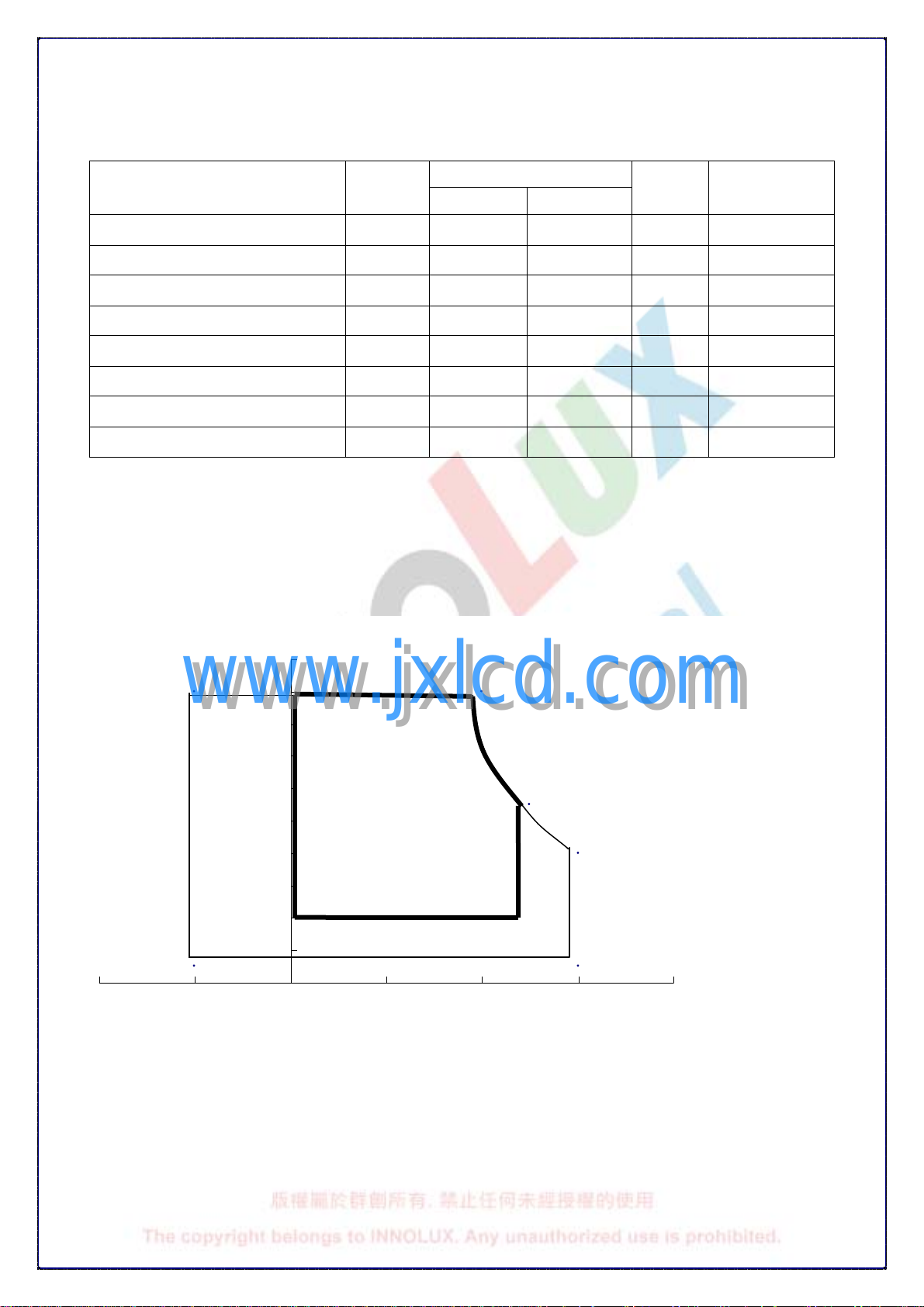
9. Packing Form
www.jxlcd.com
www.jxlcd.com
SPEC NO.
PAGE
BT 1 33HG03 V. 0
26/28
PCBA at
bottom side
ALL RIGHTS S TRICTLY RESERVED. ANY PORTION OF THIS PRPER SHALL NOT BE REPRODUCED, COPIED, OR
TRANSFORMED TO ANY OTHER FORMS WITHOUT PERMISSION FROM INNOLUX DISPLAY CORPORATION.
Page 29

10. Mechanical drawings
10-1 Front Side
SPEC NO.
PAGE
BT 1 33HG03 V. 0
27/ 28
24/28
www.jxlcd.com
www.jxlcd.com
ALL RIGHTS S TRICTLY RESERVED. ANY PORTION OF THIS PRPER SHALL NOT BE REPRODUCED, COPIED, OR
TRANSFORMED TO ANY OTHER FORMS WITHOUT PERMISSION FROM INNOLUX DISPLAY CORPORATION.
Page 30

10-2 Rear Side
www.jxlcd.com
www.jxlcd.com
SPEC NO.
PAGE
BT 1 33HG03 V. 0
28 / 28
25/28
ALL RIGHTS S TRICTLY RESERVED. ANY PORTION OF THIS PRPER SHALL NOT BE REPRODUCED, COPIED, OR
TRANSFORMED TO ANY OTHER FORMS WITHOUT PERMISSION FROM INNOLUX DISPLAY CORPORATION.
 Loading...