


INNOLUX DISPLAY CORPORATION
BT133HG01 LCD MODULE SPECIFICATION
( ) Preliminary Specification
(●) Final Specification
Customer Checked & Approved by
www.jxlcd.com
www.jxlcd.com
Checked by
QRA PD MKT
Date: 2008/06/05
Innolux Display Corporation
No. 160 K esyu e Rd. , Chu -Nan Site , Hsi nchu Scie nce P ark,
Chu - Nan 350, Miao - Li C ount y, Taiwan
Tel: 886- 3 7-58 6 000 Fa x: 88 6-37 -5860 60
Document Number: BT133HG01-DR4-24

Version: 1
Record of Revision
InnoLux copyright
All rights reserved,
Copying forbidden.
Version Revise Date Page
0 2007-11-28
1 2008-02-25
6 Add title “ Rear view of LCM”
7 Update Absolute maximum ratings
8 Update Typical operating conditions
9~10 Update Note 3, Note 4
www.jxlcd.com
www.jxlcd.com
16~17 Update Note 6, Note 9
All First edition to all
3 Update Contents
5 Update Pin assignment
11 Update Display color vs. input data signals
12 Update Input signal timing
14 Add Module function block
15 Update Color gamut, add the contrast ratio 350 Min.
Content
18 Update Reliability test items
20 Update Module lable
23 Update Packing form
24~25
Update Mechanical drawings
Contents:
SPEC NO.
PAGE
BT 1 33HG01
3/24
A. General specifications
B. Electrical specifications
C. Optical specifications
D. Reliability test items
E. S afet y
F. Displ a y qu ality
G. Handl ing p recau tion
H. Label
I. P acking fo r m
J. Mecha n ical drawi ngs
4
5
15
18
19
19
19
20
23
24
App e ndix
www.jxlcd.com
www.jxlcd.com
ALL RIGHTS STR ICTLY RESERVED. ANY PORTION OF THIS PAPER SHALL NOT BE REPRODUCED, COPIED, OR
TRANSFORMED TO ANY OTHER FORMS WITHOUT PERMISSIO N FROM INNOLUX DISPLAY CORPORATION.
A. General specifications
NO. Item Specification Remark
1 Display resolution (pixel) 1280(H) X 800(V), WXGA resolution
2 Active area (mm) 286.08(H) X 17 8 . 8 0 ( V)
3 Screen size (inch) 13.3 inches diagonal
4 Pixel pitch (mm) 0.2235(H) X 0.2235(V)
5 Color configuration R, G, B vertical stripe
6 Overall dimension (mm) 2 9 9 . 0 (W ) X 195.0(H) X 5 . 5 ( D ) (max)
7 Weight (g) 355 Max.
8 Surface treatment Hard coating 2H
SPEC NO.
PAGE
BT 1 33HG01
4/24
9 Input color signal 6 bit LVDS
10 Display colors 262K (6 bit)
11 Optimum viewing direction 6 o’clock
12 Backlight 1 CCFL
13 RoHS RoHS compliance
www.jxlcd.com
www.jxlcd.com
ALL RIGHTS STR ICTLY RESERVED. ANY PORTION OF THIS PAPER SHALL NOT BE REPRODUCED, COPIED, OR
TRANSFORMED TO ANY OTHER FORMS WITHOUT PERMISSIO N FROM INNOLUX DISPLAY CORPORATION.
B. Electrical specifications
1. Pin assignment
a. Panel connector
Connector Part No.: DF19KR-20P-1H (HIROSE) or equivalent
User’s connector Part No: DF-19G-20S-1SD or equivalent
Pin No Symbol Description Remark
1 GND Ground
2 VCC Power Supply (+3.3V)
SPEC NO.
PAGE
BT 1 33HG01
5/24
3
4
5 NC No Connection
6
7
8 Rxin0- Differential Data Input
9 Rxin0+ Differential Data Input
10 GND Ground
www.jxlcd.com
www.jxlcd.com
11 Rxin1- Differential Data Input
12 Rxin1+ Differential Data Input
13 GND Ground
14 Rxin2- Differential Data Input
15 Rxin2+ Differential Data Input
VCC
V
EDID
Clk
DATA
EDID
EDID
Power Supply (+3.3V)
DDC Power +3.3V
DDC Clock
DDC Data
R0~R5,G0
G1~G5,B0,B1
B2~B5,DE,Hsync,Vsync
16 GND Ground
17 CLK- Differential Clock Input
18 CLK+ Differential Clock Input
19 GND Ground
20 GND Ground
ALL RIGHTS STR ICTLY RESERVED. ANY PORTION OF THIS PAPER SHALL NOT BE REPRODUCED, COPIED, OR
TRANSFORMED TO ANY OTHER FORMS WITHOUT PERMISSIO N FROM INNOLUX DISPLAY CORPORATION.
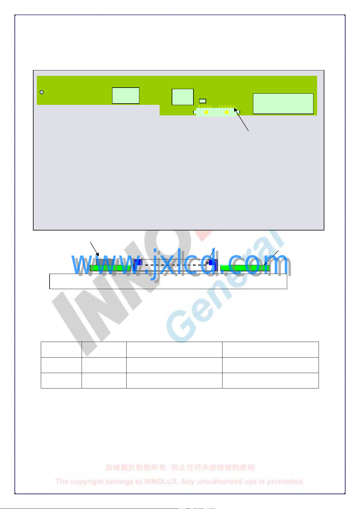
Connector :
DF19KR
-
20P-1H
VCOM
Rear view of LCM
VR
Components
www.jxlcd.com
www.jxlcd.com
TFT
b. Backlight connector
T-CON
LVDS Connector
EEPROM
SPEC NO.
PAGE
BT 1 33HG01
6/24
DC/DC
Connector Part No.: JST BHSR-02VS-1 or equivalent
Pin no. Symbol Description Remark
1 VIH Lamp high voltage input Cable color: Pink
2 VIL Lamp low voltage input Cable color: White
ALL RIGHTS STR ICTLY RESERVED. ANY PORTION OF THIS PAPER SHALL NOT BE REPRODUCED, COPIED, OR
TRANSFORMED TO ANY OTHER FORMS WITHOUT PERMISSIO N FROM INNOLUX DISPLAY CORPORATION.

Values
2. Absolute maximum ratings
SPEC NO.
PAGE
BT 1 33HG01
7/24
Parameter Symbol
Power input voltage VCC - 0.3 4.0 V At 25°C
Input signal voltage VIN - 0.3 4.0 V At 25°C
Operating temperature Top 0 50 °C Note 1
Storage temperature TST - 20 60 °C Note 2
Lamp current IL 2 7 mA
Lamp voltage VL - 2.5 KV
Re-screw - 5 Times
Assured torque at side mount - 2 kgf.cm
Note 1:
The relative humidity must not exceed 90% non-condensing at temperatures of 40°C or
less. At temperatures greater than 40°C, the wet bulb temperature must not exceed
39°C.
Note 2:
The unit should not be exposed to corrosive chemicals.
www.jxlcd.com
Relative Humidity (%RH)
-40 -20 0 20 40 60 80
www.jxlcd.com
100
90
80
70
60
50
40
30
20
10
Operation Range
Storage Range
0
Temperature(°C)
Min. Max.
Unit
rms
Remark
ALL RIGHTS STR ICTLY RESERVED. ANY PORTION OF THIS PAPER SHALL NOT BE REPRODUCED, COPIED, OR
TRANSFORMED TO ANY OTHER FORMS WITHOUT PERMISSIO N FROM INNOLUX DISPLAY CORPORATION.

=1.2V,
Note 2
=1.2V,
Note 2
3. Electrical characteristics
a. Typical operating conditions
SPEC NO.
PAGE
BT 1 33HG01
8/24
Item Symbol
Power input voltage V
Permissive power input ripple
Power input current
Power consumption
Differential input high
threshold voltage
Differential input low
LVDS
Interface
Note 1:
threshold voltage
Common input
voltage
Terminating resistor
Rush current
The specified input current and power consumption are under the Vcc =3.3 V, 25 °C,
Min. Typ. Max. Unit Remark
3 3.3 3.6
CC
V
- - 0.1 V
RF
I
- 230 260
CC
P
- 0.76 0.86
C
V
- - +100 mV
LVTH
V
-100 - - mV
LVTL
V
1.125 1.25 1.375 V Note 2
LVC
RT 90 100 110 ohm
I
Rush
- - 1.5
V
mA Note 1
Watts Note 1
V
LVC
V
LVC
A Note 3
fV=60Hz (frame frequency) condition whereas black pattern is displayed.
www.jxlcd.com
Note 2:
LVDS waveform diagram
Rxin+/CLK+
Rxin-/CLK-
www.jxlcd.com
GND
V
LVTH
V
LVTL
V
LVC
ALL RIGHTS STR ICTLY RESERVED. ANY PORTION OF THIS PAPER SHALL NOT BE REPRODUCED, COPIED, OR
TRANSFORMED TO ANY OTHER FORMS WITHOUT PERMISSIO N FROM INNOLUX DISPLAY CORPORATION.
%
%
V
Note 3:
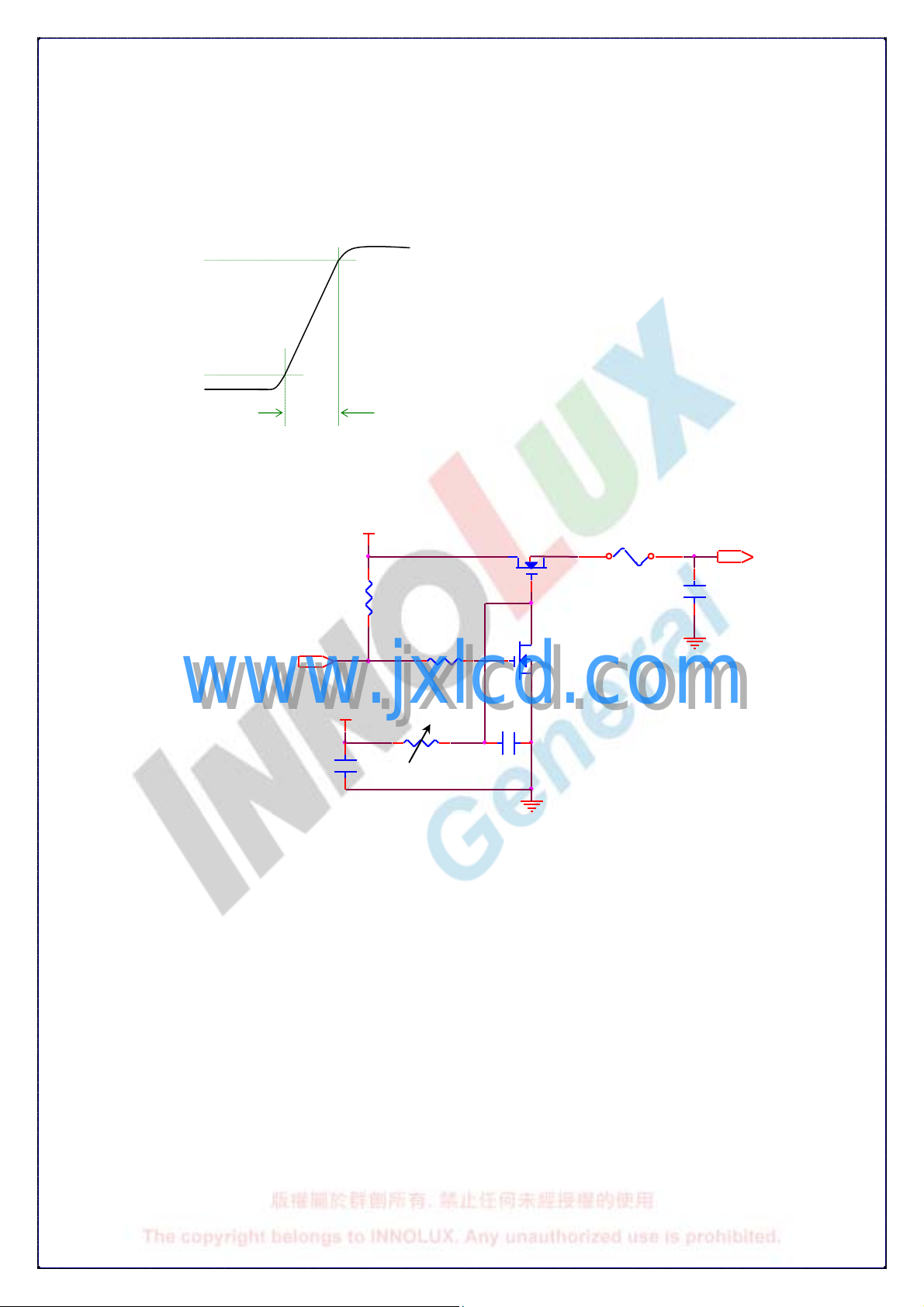
Test condition
(1) Pattern: Black pattern
(2) VCC = 3.3 V, VCC rising time = 470 μs ± 10%
SPEC NO.
PAGE
BT 1 33HG01
9/24
90
CC
10
Ton=470μs±10%
(3) Test circuit
C2
M1
2SK1059
M2
2SK1399
FUSE
VCC ( LCD input)
C1
1uF
3.3 V
R1
47K
Control signal
(High to low)
www.jxlcd.com
www.jxlcd.com
12V
R2
1K
R3
C3
1uF
47K
10000pF
ALL RIGHTS STR ICTLY RESERVED. ANY PORTION OF THIS PAPER SHALL NOT BE REPRODUCED, COPIED, OR
TRANSFORMED TO ANY OTHER FORMS WITHOUT PERMISSIO N FROM INNOLUX DISPLAY CORPORATION.

1
2
3
4
5
6
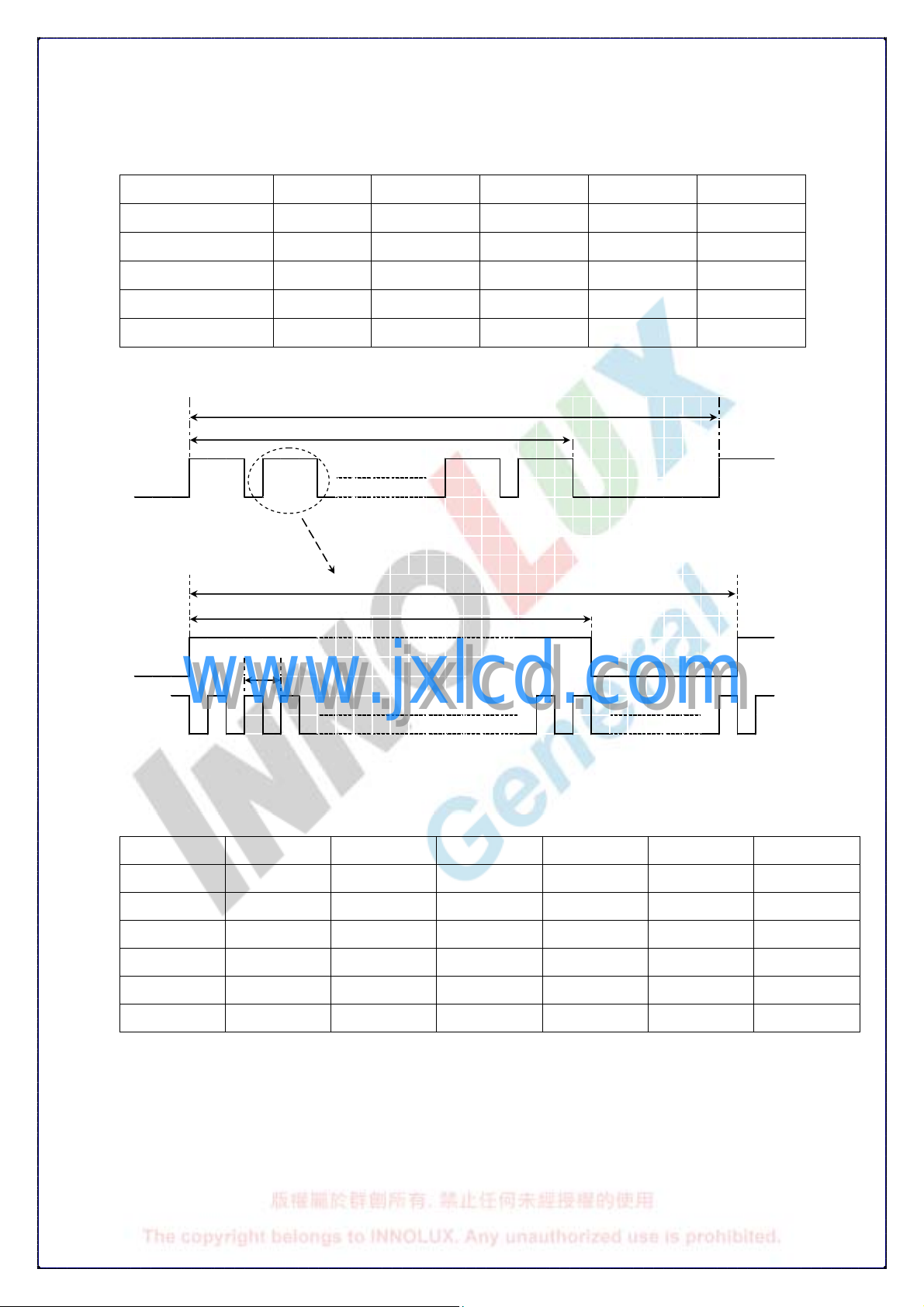
Note 4: Power sequence
SPEC NO.
PAGE
BT 1 33HG01
10/24
Power supply for LCD,
VCC
Interface data signal, Vi
(LVDS signal of transmitter)
Backlight on/off
Power sequence timing table
Parameter
Min. Typ. Max.
T1 0.5 - 10 ms
0V
10%
90%
T
0V
Value
90%
10%
T
T
T
Valid Data
T
Lamp On OFF OFF
T
T
7
Units
T2 0 - 50 ms
T3 200 - - ms
www.jxlcd.com
www.jxlcd.com
T4 200 - - ms
T5 0 - 50 ms
T6 0 - 10 ms
T7 200 - - ms
ALL RIGHTS STR ICTLY RESERVED. ANY PORTION OF THIS PAPER SHALL NOT BE REP RODUCED, COPIED, OR
TRANSFORMED TO ANY OTHER FORMS WITHOUT PERMISSIO N FROM INNOLUX DISPLAY CORPORATION.
pixel data. Each red pixel's brightness data
pixel data. Each green pixel's brightness
pixel data. Each blue pixel's brightness
b. Display color vs. input data signals
Signal Name Description Remark
SPEC NO.
PAGE
BT 1 33HG01
11/24
R5 Red Data 5 (MSB)
R4 Red Data 4
R3 Red Data 3
R2 Red Data 2
R1 Red Data 1
R0 Red Data 0 (LSB)
G5 Green Data 5 (MSB)
G4 Green Data 4
G3 Green Data 3
G2 Green Data 2
G1 Green Data 1
G0 Green Data 0 (LSB)
B5 Blue Data 5 (MSB)
B4 Blue Data 4
Red-pixel Data
Green-pixel Data
Red-
consists of these 6 bits pixel data.
Green-
data consists of these 6 bits pixel data.
Blue-
data consists of these 6 bits pixel data.
B3 Blue Data 3
www.jxlcd.com
www.jxlcd.com
B2 Blue Data 2
B1 Blue Data 1
B0 Blue Data 0 (LSB)
Blue-pixel Data
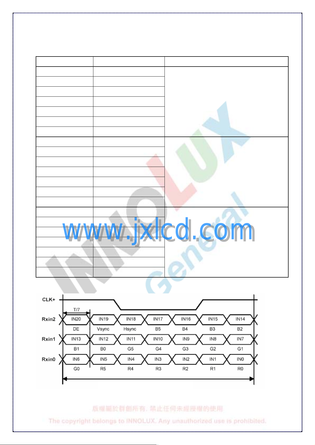
Signal for 1 DCLK cycle (t
)
CLK
ALL RIGHTS STR ICTLY RESERVED. ANY PORTION OF THIS PAPER SHALL NOT BE REP RODUCED, COPIED, OR
TRANSFORMED TO ANY OTHER FORMS WITHOUT PERMISSIO N FROM INNOLUX DISPLAY CORPORATION.
t
Vd
t
H
t
DCLK
c. Input signal timing
Timing table
Description Symbol Min Typ Max Unit
SPEC NO.
PAGE
BT 1 33HG01
12/24
Cycle time t
Line cycle time tH 1360 1440 1800
Line width-active
Frame cycle time
V width-Active tVd 800 800 800 tH
DE
DE
www.jxlcd.com
www.jxlcd.com
t
CLK
12.5 14.06 20 ns
CLK
tHd 1280 1280 1280
tV 810 823 950 tH
t
V
Hd
t
t
CLK
CLK
d. Display Position
D(1, 1) D(2, 1) …… D(640, 1) …… D(1279, 1) D(1280, 1)
D(1, 2) D(2, 2) …… D(640, 2) …… D(1279, 2) D(1280, 2)
.
.
.
D(1, 400) D(2, 400) …… D(640, 400)
.
.
.
D(1, 799) D(2, 799) …… D(640, 799)
D(1, 800) D(2, 800) …… D(640, 800)
……
……
.
.
.
.
.
.
……
…… D(1279, 400) D(1280, 400)
……
…… D(1279, 799) D(1280, 799)
…… D(1279, 800) D(1280, 800)
.
.
.
.
.
.
.
.
.
.
.
.
ALL RIGHTS STR ICTLY RESERVED. ANY PORTION OF THIS PAPER SHALL NOT BE REP RODUCED, COPIED, OR
TRANSFORMED TO ANY OTHER FORMS WITHOUT PERMISSIO N FROM INNOLUX DISPLAY CORPORATION.

e. Backlight driving conditions
Parameter Symbol Min. Typ. Max. Unit Remark
SPEC NO.
PAGE
BT 1 33HG01
13/24
Lamp voltage VL 590 640 825 V
Lamp operation
Power consumption
Lamp starting
voltage
Frequency FL 50 55 60 KHz Note 4
Lamp life time 15,000 Hr Note 5
Note 1:
The degrees of unbalance: less than 10%. (Please do not use the inverter, which has
unsymmetrical voltage and unsymmetrical current and spike wave.)
The ratio of wave height: less than ±10%
The degrees of unbalance = |IP-I-P| /I
The ratio of wave height = IP(or I-P)/I
www.jxlcd.com
Lamp should be completely turned on.
www.jxlcd.com
Note 2:
The voltage shown above should be applied to the lamp for more than 1 second
IL 2 6 7 mA
PL 1.65- 3.84 4.13 W Note 2,3,4
VLS
1300
1450 V
2
IP: high side peak
I-P: low side peak
RMS
RMS
IP
I-P
*100(%)
rms
rms
V
rms
rms
T = 25°C, Note 2,3,4
T = 0°C, Note 2,3,4
Note 1
after startup. Otherwise, the lamp may not be turned on normally.
Note 3:
Inverter should provide more than max. value, and then lamp could be completely
turned on.
Note 4:
Lamp frequency may produce interference with horizontal synchronous frequency
and this may cause line flow on the display. Therefore lamp frequency shall be
detached from the horizontal synchronous frequency and its harmonics as far as
possible in order to avoid interference.
Note 5:
Lamp life definition:
(A) Lamp current IL = 6 mA
(B) The brightness of lamp becomes 50% of the initial brightness or not normal
lighting.
rms
ALL RIGHTS STR ICTLY RESERVED. ANY PORTION OF THIS PAPER SHALL NOT BE REP RODUCED, COPIED, OR
TRANSFORMED TO ANY OTHER FORMS WITHOUT PERMISSIO N FROM INNOLUX DISPLAY CORPORATION.

oltage
f. Module function block
Gate driver
TFT-LCD
Source driver
Timing
controller
www.jxlcd.com
www.jxlcd.com
Step-up regulator
& reference v
generator
LVDS connector
SPEC NO.
PAGE
EDID
EEPROM
BT 1 33HG01
14/24
LVDS DATA BUS RSDS & CONTROL BUS POWER I2C BUS
Backlight lamp
Backlight
connector
ALL RIGHTS STR ICTLY RESERVED. ANY PORTION OF THIS PAPER SHALL NOT BE REP RODUCED, COPIED, OR
TRANSFORMED TO ANY OTHER FORMS WITHOUT PERMISSIO N FROM INNOLUX DISPLAY CORPORATION.
Specification
Min.
Typ.
Max.
C. Optical specifications
SPEC NO.
PAGE
BT 1 33HG01
15/24
Item Symbol Condition
Response time
Contrast ratio CR
Viewing angle
Brightness
(5 points average)
Color chromaticity (CIE)
Unit
Tr+Tf θ= 0∘
θ= 0∘
Top
Bottom
Left
Right
YL 200 220 nit Note 3,6
Wx
Wy
Rx
Ry
Gx
CR≧10
CR≧10
CR≧10
CR≧10
θ= 0∘
350 Note 3,5
20
30
45
45
-0.03
25 ms Note 4
deg Note 3,5,7
0.313
0.329
0.595
0.345
0.320
+0.03
Note 3
Remark
Gy
Bx
www.jxlcd.com
www.jxlcd.com
Color Gamut NTSC CIE1931 40 45 % -
White uniformity (13)
Cross talk Ct 2% Note 9
Note 1: Ambient temperature = 25°C.
Note 2: To be measured in dark room after backlight warm up 30 minutes.
Note 3: To be measured with a viewing cone of 2°by Topcon luminance meter BM-5A.
Note 4: Definition of response time:
The output signals of BM-7 are measured when the input signals are changed from
“Black” to “White” (falling time) and from “White” to “Black” (rising time), respectively.
The response time interval is between 10% and 90% of amplitudes. Refer to figure as
By
δW 0.65 0.70 Note 3,8
0.555
0.155
0.145
ALL RIGHTS STR ICTLY RESERVED. ANY PORTION OF THIS PAPER SHALL NOT BE REP RODUCED, COPIED, OR
TRANSFORMED TO ANY OTHER FORMS WITHOUT PERMISSIO N FROM INNOLUX DISPLAY CORPORATION.
below.

Contrast ratio (CR)
=
δ
Minimum Brightness of
thirteen
points
Maximum Brightness of
thirteen
points
SPEC NO.
PAGE
BT 1 33HG01
16/24
100%
S
i
90%
g
n
a
l
(
R
e
l
a
t
i
v
e
v
a
l
u
10%
e
)
0%
Note 5: Definition of contrast ratio:
Contrast ratio is calculated with the following formula:
Note 6: Driving conditions for CCFL: IL= 6.0 mA
Luminance are measured at the following thirteen points (1~13):
YL = (Y5+Y10+Y11+Y12+Y13) / 5
Note 7: Definition of viewing angle
www.jxlcd.com
www.jxlcd.com
Tr
Brightness on the "white" state
Brightness on the "black" state
"Black"
, 55 KHz Frequency.
rms
"White""White"
Tf
Note 8: Definition white uniformity:
Luminance are measured at the following thirteen points (1~13):
ALL RIGHTS STR ICTLY RESERVED. ANY PORTION OF THIS PAPER SHALL NOT BE REP RODUCED, COPIED, OR
TRANSFORMED TO ANY OTHER FORMS WITHOUT PERMISSIO N FROM INNOLUX DISPLAY CORPORATION.

2 3
4
5 6
7
8 9
W
L
SPEC NO.
PAGE
BT 1 33HG01
17/24
Note 9:
10 mm
1/4 W
1/2 W
1/4 W
10mm
10 mm
1
12
1/4 L
10
1/2 L
11
13
1/4 L
10 mm
1/2
1/6
2/3
A
1/6
A’
32 gray level 32 gray level
B
1/2
1/2
1/3
1/6
1/6
1/3
1/2
B’
2/3
www.jxlcd.com
www.jxlcd.com
Unit: percentage of dimension of display area
l LA-LA’ l / LA x 100%= 2% max., LA and LA’ are brightness at location A and A’
l LB-LB’ l / LB x 100%= 2% max., LB’ and LB’ are brightness at location B and B’
0 gray level
ALL RIGHTS STR ICTLY RESERVED. ANY PORTION OF THIS PAPER SHALL NOT BE REP RODUCED, COPIED, OR
TRANSFORMED TO ANY OTHER FORMS WITHOUT PERMISSIO N FROM INNOLUX DISPLAY CORPORATION.
to
one
D. Reliability test items
Test Item Test Condition Judgment Remark
SPEC NO.
PAGE
BT 1 33HG01
18/24
High temperature storage
Low temperature storage
High temperature & high
humidity operation
High temperature operation
Low temperature operation
Thermal Shock
(Non-operation)
Electrostatic discharge
(ESD)
Vibration
(Sine wave, non-operation)
Mechanical shock
(Non-operation)
60°C, 240 hours
-20°C, 240 hours
40°C, 90%RH, 240 hours
(No condensation)
50°C, 240 hours Note 1 Note 2
0°C, 240 hours Note 1 Note 2
-25°C/30 mins ~ 65°C/30 mins 100 cycles Note 1 Note 2
150 pF,330Ω,
Contact: ±8kV,Air: ±15kV
Sinusoidal vibration, 3G zero-to-peak, 5
150 Hz, 0.37 octave/minute; 0.5hr in each
perpendicular axes.
200G/2ms, Half sine wave, ±X, ±Y, ±Z
time for each direction
Note 1 Note 2
Note 1 Note 2
Note 1 Note 2
Note 1
Note 1 Note 2
Note 1 Note 2
Note 1:
www.jxlcd.com
Pass: Normal display image with no obvious non-uniformity and no line defect.
Fail: No display image, obvious non-uniformity, or line defects.
Note 2:
Evaluation should be tested after storage at room temperature for one hour.
www.jxlcd.com
Partial transformation of the module parts should be ignored.
ALL RIGHTS STR ICTLY RESERVED. ANY PORTION OF THIS PAPER SHALL NOT BE REP RODUCED, COPIED, OR
TRANSFORMED TO ANY OTHER FORMS WITHOUT PERMISSIO N FROM INNOLUX DISPLAY CORPORATION.

E. Safety
1. Sharp edge requirements
There will be no sharp edges or corners on the display assembly that could cause injury.
2. Materials
a. Toxicity
There will be no carcinogenic materials used anywhere in the display module. If toxic
materials are used, they will be reviewed and approved by the responsible InnoLux
Toxicologist.
b. Flammability
All components including electrical components that do not meet the flammability grade
UL94-V0 in the module will complete the flammability rating exception approval process.
The printed circuit board will be made from material rated 94-V0 or better. The actual UL
SPEC NO.
PAGE
BT 1 33HG01
19/24
flammability rating will be printed on the printed circuit board.
c. Capacitors
If any polarized capacitors are used in the display assembly, provisions will be made to
keep them from being inserted backwards.
F. Display quality
The display quality of the color TFT-LCD module should be in compliance with the
InnoLux incoming inspection standard.
G. Handling precaution
The handling of the TFT-LCD should be in compliance with the InnoLux handling principle
standard.
www.jxlcd.com
www.jxlcd.com
ALL RIGHTS STR ICTLY RESERVED. ANY PORTION OF THIS PAPER SHALL NOT BE REP RODUCED, COPIED, OR
TRANSFORMED TO ANY OTHER FORMS WITHOUT PERMISSIO N FROM INNOLUX DISPLAY CORPORATION.
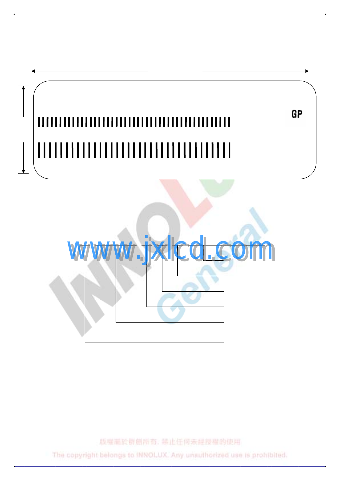
Serial
No
IIII
NNO
NNONNO
NNO
LLLL
UX
UXUX
UX
H. Label
1. Module label
SPEC NO.
PAGE
BT 1 33HG01
20/24
28 mm
BT133HG01 V.1
AB1330001 01X
Z1 Z2 Z3 Z4 Z
*’P1’P2’Y3’W4’W5’S6’S7’S8’S9’E10’E11’E12’R13*
--Z 7--Z8 Z9 Z10 Z
5 Z 6
83 mm
a. Model name : BT133HG01
b. Version : V.1
c. Product Number : AB133000101X (INL internal use)
d. Serial ID : Z1 Z2 Z3 Z4 Z 5 Z 6 Z 7 Z8 Z
11 Z 12
9 Z10
Z
11
Z
MADE IN CHINA
12
www.jxlcd.com
www.jxlcd.com
Serial ID includes the information as below:
(1) Manufactured Date: Year: 0~9, for 2000~2009
(2) Month: 1~9 & A~C for Jan. ~ Dec.
(3) Date: 1~9 & A~Z (exclude I, O, Q, U) for 1th~31th
(4) Code of grade: 1, 3, 5, 7
(5) Serial No: Module manufacture sequential no
Code of grade
INL internal use
INL internal use
Year, Month, Date
INL internal use
ALL RIGHTS STR ICTLY RESERVED. ANY PORTION OF THIS PAPER SHALL NOT BE REP RODUCED, COPIED, OR
TRANSFORMED TO ANY OTHER FORMS WITHOUT PERMISSIO N FROM INNOLUX DISPLAY CORPORATION.

Serial
No
2. Carton label
SPEC NO.
PAGE
BT 1 33HG01
21/24
INNOLUX DISPLAY
BOX ID:
100 mm
Z
Model No. BT133HG01 V.1
AB133000101X
Quantity : 25 PCS
MFG Date: 20XX/XX/XX Made in XXX
QC:
120 mm
1 Z2 Z 3
Z
-- Z 5-- Z 6 Z 7 Z
4
8 Z9
a. Model name : BT133HG01
b. Version : V.1
c. Packing quantity : 25 pcs
d. Serial ID : Z1 Z2 Z3 Z4 Z 5 Z6 Z
www.jxlcd.com
www.jxlcd.com
Z 9
7 Z8
Code of grade
Year, Month, Date
Serial ID includes the information as below:
(1) Manufactured Date: Year: 0~9, for 2000~2009
Month: 1~9 & A~C for Jan. ~Dec.
Date: 1~9 & A~Z (exclude I, O, Q, U) for 1th~31th
(2) Code of grade: 1, 3, 5, 7, E
INL internal use
(3) Serial No: Module packing sequential no
ALL RIGHTS STR ICTLY RESERVED. ANY PORTION OF THIS PAPER SHALL NOT BE REP RODUCED, COPIED, OR
TRANSFORMED TO ANY OTHER FORMS WITHOUT PERMISSIO N FROM INNOLUX DISPLAY CORPORATION.

I. Packing form
SPEC NO.
PAGE
BT 1 33HG01
22/24
www.jxlcd.com
www.jxlcd.com
ALL RIGHTS STR ICTLY RESERVED. ANY PORTION OF THIS PAPER SHALL NOT BE REP RODUCED, COPIED, OR
TRANSFORMED TO ANY OTHER FORMS WITHOUT PERMISSIO N FROM INNOLUX DISPLAY CORPORATION.

BT 1 33HG01 V. 0
24/25
www.jxlcd.com
www.jxlcd.com
SPEC NO.
PAGE
J. Mechanical drawings
ALL RIGHTS STRICTLY RESERVED. ANY PORTION OF THIS PRPER SHALL N OT BE REPRODUCED, COP IED, OR TRANSFORMED TO ANY OTHER FORMS WITHOUT
PERMISSION FROM INNOLUX DISPLAY CORPORATION.

BT 1 33HG01 V. 0
25/25
www.jxlcd.com
www.jxlcd.com
SPEC NO.
PAGE
ALL RIGHTS STRICTLY RESERVED. ANY PORTION OF THIS PRPER SHALL N OT BE REPRODUCED, COP IED, OR TRANSFORMED TO ANY OTHER FORMS WITHOUT
PERMISSION FROM INNOLUX DISPLAY CORPORATION.
 Loading...