

Page 1

INNOLUX DISPLAY CORPORATION
BT101IW02 V.0 LCD MODULE SPECIFIC ATION
(●) Preliminary Specification
( ) Final Specification
Customer Checked & Approved by
Approved by Checked by Prepared by
MKT PD PM
www.jxlcd.com
www.jxlcd.com
Innolux Display Corporation
No. 160 K esyu e Rd. , Chu -Nan Site , Hsi nchu Scie nce P ark,
Chu - Nan 350, Miao - Li C ount y, Taiwan
Tel: 886- 3 7-58 6 000 Fa x: 88 6-37 -5860 60
Date: 2009/04/13
Page 2

Version: 0.0
InnoLux copyright
All rights reserved,
Copying forbidden.
Record of Revision
Version Revise Date P a g e
0.0
2009/04/10
All First Edition issued
Content
www.jxlcd.com
www.jxlcd.com
Page 3
Contents: Page
SPEC NO.
PAGE
BT 1 01IW 0 1 V. 0
1/ 2 3
1. General Specifications
2. Electrical Specifications
2-1 Pin Assignment
2-2 Absolute Maximum Ratings
2-3 Electrical Characteristics
3. Optical Specifications
4. Reliability Test Items
5. S afet y
6. D ispl a y Quality
7. H andling P recaution
8. L abel Defi nitio n
2
3
5
6
14
17
18
18
18
19
9. P ackin g Fo r m
10. Mech anical Draw ings
www.jxlcd.com
www.jxlcd.com
21
22
ALL RIGHTS STRICTLY RES ERVED. ANY PORTION OF THIS PRPER S HALL NOT BE REPRODUCED, COPIED, OR
TRANSFORMED TO ANY OTHER FORMS W ITHOUT PERMISSION FROM INNOLUX DISP LAY CORPORATION.
Page 4
1. General Specifications
NO. Item Specification Unit
SPEC NO.
PAGE
BT 1 01IW 0 1 V. 0
2/ 2 3
1 Display resolution (pixel)
2 Active area
3 Screen size 10.1 inches diagonal Inches
4 Pixel pitch 217.5x208.8 um
5 Color configuration R, G, B vertical stripe
6 Overall dimension
7 Weight
8 Surface treatment Glare
9 Input color signal 6 bit LVDS
10 Display colors 262K (6 bit)
11
12 Backlight W-LED
13 Glass thicknes s 0.5
Optimum viewing
direction
1024(H) X 600(V), SD resolution
222.72(H) X 125.28(V)
235 (W) X 143(H) X 5.2(D) (max)
190Max.
6 o’clock
mm
mm
Grams
mm
www.jxlcd.com
LED life time wi t h
13
14 RoHS RoHS compliance
www.jxlcd.com
module
12,000 (min), T=25°°°°C hrs
ALL RIGHTS STRICTLY RES ERVED. ANY PORTION OF THIS PRPER S HALL NOT BE REPRODUCED, COPIED, OR
TRANSFORMED TO ANY OTHER FORMS W ITHOUT PERMISSION FROM INNOLUX DISP LAY CORPORATION.
Page 5
2. Electrical Specifications
2-1 Pin Assignment
a. Panel connector
Connector Part No.: 20455-040E-0* or equivalent
User’s connector Part No: 20455-040E-0* or equivalent
PIN NO
1 NC No connection (Reserve)
2 VCC Power Supply (+3.3V)
3 VCC Power Supply (+3.3V)
4 V
5 NC No connection (Reserve)
6 Clk
7 DATA
8 Rxin0- - Differential data input
9 Rxin0+ + Differential data input
10 GND Ground
11 Rxin1- - Differential data input
12 Rxin1+ + Differential data input
13 GND Ground
14 Rxin2- - Differential data input
15 Rxin2+ + Differential data input
16 GND Ground
17 CLK- - Differential clock input
18 CLK+ + Differential clock input
19 GND Ground
20 NC No connection (Reserve)
21 NC No connection (Reserve)
22 GND Ground
23 NC No connection (Reserve)
24 NC No connection (Reserve)
25 GND Ground
26 NC No connection (Reserve)
27 NC No connection (Reserve)
28 GND Ground
29 NC No connection (Reserve)
30 NC No connection (Reserve)
31 LED_GND LED Ground
32 LED_GND LED Ground
33 LED_GND LED Ground
34 NC No connection (Reserve)
35 LED_PWM
36 LED_EN LED enable pin (3.3V)
37 NC No connection (Reserve)
38 V_LED LED power supply 7.5V~21V
39 V_LED LED power supply 7.5V~21V
40 V_LED LED power supply 7.5V~21V
Symbol Function Remark
DDC Power +3.3V
EDID
DDC Clock
EDID
DDC Data
EDID
www.jxlcd.com
www.jxlcd.com
PWM dimming signal input
SPEC NO.
PAGE
BT 1 01IW 0 1 V. 0
3/ 2 3
R0~R5,G0
G1~G5,B0,B1
B2~B5,DE,Hsync,Vsync
ALL RIGHTS STRICTLY RES ERVED. ANY PORTION OF THIS PRPER S HALL NOT BE REPRODUCED, COPIED, OR
TRANSFORMED TO ANY OTHER FORMS W ITHOUT PERMISSION FROM INNOLUX DISP LAY CORPORATION.
Page 6

b. General Block Diagram
VR
DC/DC
DC/DC
www.jxlcd.com
www.jxlcd.com
20455-040
Pin1
T-CON
Connector plug in direction
SPEC NO.
PAGE
BT 1 01IW 0 1 V. 0
4/ 2 3
FPC
LED
Driver
ALL RIGHTS STRICTLY RES ERVED. ANY PORTION OF THIS PRPER S HALL NOT BE REPRODUCED, COPIED, OR
TRANSFORMED TO ANY OTHER FORMS W ITHOUT PERMISSION FROM INNOLUX DISP LAY CORPORATION.
Page 7
Values
Min.
Max.
Storage Range
2-2. Absolute Maximum Ratings
SPEC NO.
PAGE
BT 1 01IW 0 1 V. 0
5/ 2 3
Parameter Symbol
Power input voltage VCC - 0.3 4.0 V At 25°C
Input signal voltage VIN - 0.3 4.0 V At 25°C
LED input voltage V
Operating temperature Top 0 50 °C Note 1
Storage temperature TST - 20 60 °C Note 2
Re-screw - 5 Times
Assured torque at side mount - 2 kgf.cm
Note 1: The relative humidity must not exceed 90% non-condensing at temperatures of 40°C or
less. At temperatures greater than 40°C, the wet bulb temperature must not exceed 39°C.
Note 2: The unit should not be exposed to corrosive chemicals.
Relative Humidity (%RH)
-40 -20 0 20 40 60 80
www.jxlcd.com
www.jxlcd.com
100
90
80
70
60
50
40
30
20
10
Operation Range
0
Temperature (°C)
- 0.3 30 V At 25℃
LED
Unit
Remark
ALL RIGHTS STRICTLY RES ERVED. ANY PORTION OF THIS PRPER S HALL NOT BE REPRODUCED, COPIED, OR
TRANSFORMED TO ANY OTHER FORMS W ITHOUT PERMISSION FROM INNOLUX DISP LAY CORPORATION.
Page 8

2-3. Electrical Characteristics
a. Typical operating conditions
SPEC NO.
PAGE
BT 1 01IW 0 1 V. 0
6/ 2 3
Item Symbol
Power input voltage
Permissive power input ripple
Power input current
Power consumption
Differential input high
threshold voltage
Differential input low
LVDS
interface
Initial inrush current
Stable rush current
threshold voltage
Common input
voltage
Terminating resistor
www.jxlcd.com
www.jxlcd.com
Min. Typ. Max. Unit Remark
V
3 3.3 3.6 V
CC
V
- - 0.1 V
RF
I
- 220 400 mA Note 1
CC
P
- 0.65 1 Watts Note 1
logic
V
V
- - +100 mV
LVTH
V
-100 - - mV
LVTL
V
0.1 1.2 1.4 V Note 2
LVC
RT 90 100 110 Ohm
I
- - 1.5 A
inrush
I
- - 0.0025 A2sec
st-rush
LVC
V
LVC
=1.2V,
Note 2
=1.2V,
Note 2
Note 3
LED Initial inrush current
LED stable rush current
Note 1: The specified input current and power consumption are under the Vcc =3.3 V, 25 °C,
fV=60Hz (frame frequency) condition whereas black pattern is displayed.
Note 2 LVDS waveform diagram
Rxin+/CLK+
Rxin-/CLK-
I
LED-inrush
I
LED-st-inrush
- - 3.0 A
- - 0.0075 A2sec
V
LVC
GND
Note 4
V
LVTH
V
LVTL
ALL RIGHTS STRICTLY RES ERVED. ANY PORTION OF THIS PRPER S HALL NOT BE REPRODUCED, COPIED, OR
TRANSFORMED TO ANY OTHER FORMS W ITHOUT PERMISSION FROM INNOLUX DISP LAY CORPORATION.
Page 9

90%
10%
Ton=470µs±10%
V
90%
10%
Ton=470µs±10%
V
_LED
Note 3 Test condition
(1) Pattern: Black pattern
(2) VCC = 3.3 V, VCC rising time = 470 μs ± 10%
SPEC NO.
PAGE
BT 1 01IW 0 1 V. 0
7/ 2 3
Control signal
(High to low)
CC
(3) Test circuit
3.3 V
R1
47K
R2
www.jxlcd.com
www.jxlcd.com
12V
C3
1uF
1K
R3
47K
M1
2SK1059
C2
10000pF
M2
2SK1399
FUSE
C1
1uF
VCC ( LCD input)
Note 4 Test condition
ALL RIGHTS STRICTLY RES ERVED. ANY PORTION OF THIS PRPER S HALL NOT BE REPRODUCED, COPIED, OR
TRANSFORMED TO ANY OTHER FORMS W ITHOUT PERMISSION FROM INNOLUX DISP LAY CORPORATION.
(1) Pattern: LED duty 100%
(2) V_LED = 12.0V, V_LED rising time = 470 μs ± 10%
Page 10

(3) Test circuit
21V
C3
1uF
12 V
R1
47K
R3
47K
R2
1K
C2
10000pF
Control signal
(High to low)
M1
2SK1059
M2
2SK1399
SPEC NO.
PAGE
FUSE
BT 1 01IW 0 1 V. 0
8/ 2 3
V_LED
C1
1uF
b. Power sequence
Power supply for LCD, V
www.jxlcd.com
www.jxlcd.com
Interface data signal, Vi
(LVDS signal of transmitter)
Backlight on/off
Power sequence timing table
CC
0V
10%
90%
0V
90%
10%
T
T
1
2
T
5
7
6
T
T
Valid Data
T
3
T
4
Lamp On OFF OFF
Parameter
Units
Min. Typ. Max.
T1 0.5 - 10 ms
T2 0 - 50 ms
T3 200 - - ms
T4 200 - - ms
T5 0 - 50 ms
T6 0 - 10 ms
T7 400 - - ms
ALL RIGHTS STRICTLY RES ERVED. ANY PORTION OF THIS PRPER S HALL NOT BE REPRODUCED, COPIED, OR
TRANSFORMED TO ANY OTHER FORMS W ITHOUT PERMISSION FROM INNOLUX DISP LAY CORPORATION.
Value
Page 11

pixel data. Each red pixel's brightness data
pixel data. Each green pixel's brightness
data. Each blue pixel's brightness data
c. Display color vs. input data signals
Signal Name Description Remark
SPEC NO.
PAGE
BT 1 01IW 0 1 V. 0
9/ 2 3
R5 Red Data 5 (MSB)
R4 Red Data 4
R3 Red Data 3
R2 Red Data 2
R1 Red Data 1
R0 Red Data 0 (LSB)
Red-pixel Data
G5 Green Data 5 (MSB)
G4 Green Data 4
G3 Green Data 3
G2 Green Data 2
G1 Green Data 1
G0 Green Data 0 (LSB)
Green-pixel Data
B5 Blue Data 5 (MSB)
B4 Blue Data 4
B3 Blue Data 3
B2 Blue Data 2
Redconsists of these 6 bits pixel data.
Greendata consists of these 6 bits pixel data.
Blue-pixel
consists of these 6 bits pixel data.
B1 Blue Data 1
B0 Blue Data 0 (LSB)
www.jxlcd.com
www.jxlcd.com
Blue-pixel Data
Signal for 1 DCLK cycle (t
)
CLK
ALL RIGHTS STRICTLY RES ERVED. ANY PORTION OF THIS PRPER S HALL NOT BE REPRODUCED, COPIED, OR
TRANSFORMED TO ANY OTHER FORMS W ITHOUT PERMISSION FROM INNOLUX DISP LAY CORPORATION.
Page 12

d. Input signal timing
Timing table
Description Symbol Min Typ Max Unit
Frame rate -- --- 60 --- Hz
SPEC NO.
PAGE
BT 1 01IW 0 1 V. 0
10/ 2 3
Clock freq. 1/t
Line cycle time tH (1074) 1212 (1400)
Line width-active
Frame cycle time
V width-active tVd --- 600 --- tH
DE
DE
DCLK
www.jxlcd.com
www.jxlcd.com
t
CLK
(40) 46.4 (55) MHz
CLK
tHd --- 1024 ---
tV (620) 638 (654) tH
t
V
t
Vd
t
H
t
Hd
t
t
CLK
CLK
e. Display position
D(1, 1) D(2, 1) …… D(673, 1) …… D(1023, 1) D(1024, 1)
D(1, 2) D(2, 2) …… D(673, 2) …… D(1023, 2) D(1024, 2)
.
.
.
D(1, 384) D(2, 300) …… D(673, 384)
.
.
.
D(1, 767) D(2, 599) …… D(673, 599)
D(1, 768) D(2, 600) …… D(673, 600)
ALL RIGHTS STRICTLY RES ERVED. ANY PORTION OF THIS PRPER S HALL NOT BE REPRODUCED, COPIED, OR
TRANSFORMED TO ANY OTHER FORMS W ITHOUT PERMISSION FROM INNOLUX DISP LAY CORPORATION.
……
……
.
.
.
.
.
.
……
…… D(1023, 300) D(1024, 300)
……
…… D(1023, 599) D(1024, 599)
…… D(1023, 600) D(1024, 600)
.
.
.
.
.
.
.
.
.
.
.
.
Page 13

Timing
Step
-
up regulator
oltage
EDID
f. Backlight driving conditions
Parameter Symbol Min. Typ. Max. Unit Remark
SPEC NO.
PAGE
BT 1 01IW 0 1 V. 0
11/ 2 3
LED Forward Voltage V
LED Forward Current
LED Power consumption
Output PWM frequency
Duty ratio - 20 100 %
LED life time - 15,000 Hr T = 25°C , Note 1
Note 1: LED life time definition is Brightness decrease to 50% of initial or abnormal lighting.
g. Module function block
www.jxlcd.com
www.jxlcd.com
LED driver
controller
3 3.2 3.4 V
F
IF 20 mA
P
2.1 2.3 W
LED
F
PWM
200 20000 Hz T = 25°C
LED Light-bar
TFT-LCD
Source driver
& reference v
generator
LVDS connector
rms
rms
EEPROM
T = 25°C
T = 25°C
T = 25°C
Gate driver
LVDS DATA BUS mini-LVDS & CONTROL BUS POWER I2C BUS
ALL RIGHTS STRICTLY RES ERVED. ANY PORTION OF THIS PRPER S HALL NOT BE REPRODUCED, COPIED, OR
TRANSFORMED TO ANY OTHER FORMS W ITHOUT PERMISSION FROM INNOLUX DISP LAY CORPORATION.
Page 14

LED Drivi
ng
3
parallels
h. LED circuit block
SPEC NO.
PAGE
BT 1 01IW 0 1 V. 0
12/ 2 3
& 9 series
Circuit
FB1
FB2
www.jxlcd.com
www.jxlcd.com
LED_P
FB3
ALL RIGHTS STRICTLY RES ERVED. ANY PORTION OF THIS PRPER S HALL NOT BE REPRODUCED, COPIED, OR
TRANSFORMED TO ANY OTHER FORMS W ITHOUT PERMISSION FROM INNOLUX DISP LAY CORPORATION.
Page 15

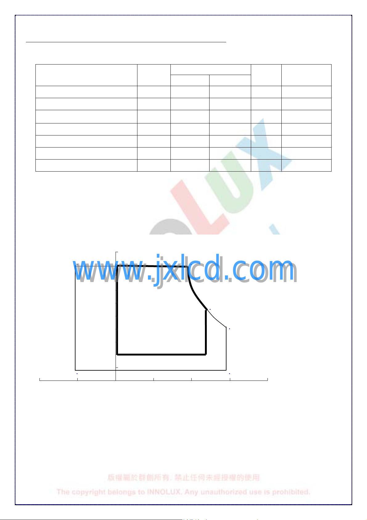
3. Optical specifications
SPEC NO.
PAGE
BT 1 01IW 0 1 V. 0
13/ 2 3
Item Symbol Condition
Response time
Contrast ratio CR
Viewing angle
Brightness
(5 points average)
Color chromaticity (CIE)
Specification
Min. Typ. Max.
Tr+Tf θ= 0∘
θ= 0∘
Top
Bottom
Left
Right
YL 150 180 nit Note 2,5
Wx
Wy
Rx
Ry
Gx
CR≧10
CR≧10
CR≧10
CR≧10
θ= 0∘
500 Note 2,4
15
30
40
40
-0.03
8 TBD ms Note 3
0.313
0.329
0.580
0.355
+0.03
0.337
Unit Remark
deg Note 2,4,6
Note 2
Gy
Bx
www.jxlcd.com
www.jxlcd.com
Color Gamut NTSC CIE1931 40 45 % -
White uniformity
Cross talk Ct 2% Note 8
Note 1: To be measured in dark room.
Note 2: To be measured with a viewing cone of 2°by Topcon luminance meter BM-5A.
Note 3: Definition of response time:
The output signals of BM-7 are measured when the input signals are changed from “Black” to
“White” (falling time) and from “White” to “Black” (rising time), respectively. The response time
interval is between 10% and 90% of amplitudes. Refer to figure as below.
By
δ
1.25
W(5)
δ
1.5
W(13)
0.581
0.163
0.097
Note 2,7
ALL RIGHTS STRICTLY RES ERVED. ANY PORTION OF THIS PRPER S HALL NOT BE REPRODUCED, COPIED, OR
TRANSFORMED TO ANY OTHER FORMS W ITHOUT PERMISSION FROM INNOLUX DISP LAY CORPORATION.
Page 16

=
Maximum Brightness of
thirteen
points
Minimum Brightness of
thirteen
points
=
Maximum Brightness of
five
points
Minimum Brightness of
five
points
Contrast ratio (
Avg of 5p
ts)
=
SPEC NO.
PAGE
BT 1 01IW 0 1 V. 0
14/ 2 3
100%
S
i
90%
g
n
a
l
(
R
e
l
a
t
i
v
e
v
a
l
u
10%
e
)
0%
Note 4: Definition of contrast ratio:
Contrast ratio is calculated with the following formula:
Note 5: Driving current for LED should be 20 mA.
Luminance are measured at the following thirteen points (1~13):
YL = (Y5+Y10+Y11+Y12+Y13) / 5
Note 6: Definition of viewing angle
Tr
L white (Avg of 5pts.)
L Black (Avg of 5pts.)
"Black"
"White""White"
Tf
www.jxlcd.com
www.jxlcd.com
Note 7: Definition white uniformity:
Luminance is measured at the following thirteen points (1~13):
δ
W(13)
δ
W(5)
ALL RIGHTS STRICTLY RES ERVED. ANY PORTION OF THIS PRPER S HALL NOT BE REPRODUCED, COPIED, OR
TRANSFORMED TO ANY OTHER FORMS W ITHOUT PERMISSION FROM INNOLUX DISP LAY CORPORATION.
Page 17

13 point measuring locations refer to the point 1,~13.
5 point measuring locations refer to the point 5,10~13.
L and W are active area dimensions. Active area center refer to attached drawing
SPEC NO.
PAGE
BT 1 01IW 0 1 V. 0
15/ 2 3
Note 8:
32 gray level 32 gray level
www.jxlcd.com
www.jxlcd.com
1/2
A
1/6
1/6
2/3
A’
1/2
1/3
1/6
B
1/2
B’
0 gray level
1/6
1/3
1/2
2/3
Unit: percentage of dimension of display area
l LA-LA’ l / LA x 100%= 2% max., LA and LA’ are brightness at location A and A’
l LB-LB’ l / LB x 100%= 2% max., LB’ and LB’ are brightness at location B and B’
ALL RIGHTS STRICTLY RES ERVED. ANY PORTION OF THIS PRPER S HALL NOT BE REPRODUCED, COPIED, OR
TRANSFORMED TO ANY OTHER FORMS W ITHOUT PERMISSION FROM INNOLUX DISP LAY CORPORATION.
Page 18

; 0.5hr in each
one
4. Reliability test items
Test Item Test Condition Judgment Remark
SPEC NO.
PAGE
BT 1 01IW 0 1 V. 0
16/ 2 3
High temperature storage
Low temperature storage
High temperature & high
humidity operation
High temperature operation 50°C, 240 hours Note 1 Note 2
Low temperature operation 0°C, 240 hours Note 1 Note 2
Thermal Shock
(Non-operation)
Electrostatic discharge (ESD)
Vibration
(Non-operation)
Mechanical shock
(Non-operation)
60°C, 240 hours
-20°C, 240 hours
40°C, 90% RH, 240 hours
(No condensation)
-25°C / 30 mins ~ 65°C / 30 mins
100 cycles
150 pF, 330Ω,
Contact: ±8kV, Air: ±15kV
1.5G, 10 to 500 Hz random
perpendicular axes ( X, Y, Z ).
220G/2ms, Half sine wave, ±X, ±Y, ±Z
time for each direction
Note 1 Note 2
Note 1 Note 2
Note 1 Note 2
Note 1 Note 2
Note 1
Note 1 Note 2
Note 1 Note 2
Note 1: Pass: Normal display image with no obvious non-uniformity and no line defect.
Fail: No display image, obvious non-uniformity, or line defects.
Note 2: Evaluation should be tested after storage at room temperature more than one hour.
www.jxlcd.com
www.jxlcd.com
Partial transformation of the module parts should be ignored.
ALL RIGHTS STRICTLY RES ERVED. ANY PORTION OF THIS PRPER S HALL NOT BE REPRODUCED, COPIED, OR
TRANSFORMED TO ANY OTHER FORMS W ITHOUT PERMISSION FROM INNOLUX DISP LAY CORPORATION.
Page 19

5. Safety
5-1. Sharp edge requirements
There will be no sharp edges or corners on the display assembly that could cause injury.
5-2. Materials
a. Toxicity
There will be no carcinogenic materials used anywhere in the display module. If toxic materials
are used, they will be reviewed and approved by the responsible InnoLux Toxicologist.
b. Flammability
All components including electrical components that do not meet the flammability grade UL94-V0
in the module will complete the flammability rating exception approval process. The printed circuit
board will be made from material rated 94-V0 or better. The actual UL flammability rating will be
printed on the printed circuit board.
SPEC NO.
PAGE
BT 1 01IW 0 1 V. 0
17/ 2 3
c. Capacitors
If any polarized capacitors are used in the display assembly, provisions will be made to keep
them from being inserted backwards.
6. Display quality
The display quality of the color TFT-LCD module should be in compliance with the InnoLux
incoming inspection standard.
www.jxlcd.com
www.jxlcd.com
7. Handling precaution
(1) Do not apply rough force such as bending or twisting to the module during assembly.
(2) To assemble or install module into user’s system can be only in clean working areas. The
dust and oil may cause electrical short or worsen the polarizer.
(3) It’s not permitted to have pressure or impulse on the module because the LCD panel and
Backlight will be damaged.
(4) Always follow the correct power sequence when LCD module is connecting and
operating.
(5) Do not pull the I/F connector in or out while the module is operating.
(6) Do not disassemble the module.
(7) Use a soft dry cloth without chemicals for cleaning, because the surface of polarizer is
very soft and easily scratched.
(8) It is dangerous that moisture come into or contacted the LCD module, because moisture
may damage LCD module when it is operating.
(9) High temperature or humidity may reduce the performance of module. Please store LCD
module within the specified storage conditions.
ALL RIGHTS S TRICTLY RESERVED. A NY PORTIO N OF THIS P RPER SHALL NOT BE REP RODUCED, COPIED, O R
TRANSFORMED TO ANY OTHER FORMS W ITHOUT PERMISSION FROM INNOLUX DISP LAY CORPORATION.
Page 20

8. Label Definition
8-1. Module label
SPEC NO.
PAGE
BT 1 01IW 0 1 V. 0
18/ 2 3
www.jxlcd.com
www.jxlcd.com
ALL RIGHTS S TRICTLY RESERVED. A NY PORTIO N OF THIS P RPER SHALL NOT BE REP RODUCED, COPIED, O R
TRANSFORMED TO ANY OTHER FORMS W ITHOUT PERMISSION FROM INNOLUX DISP LAY CORPORATION.
Page 21

8-2. Carton label
SPEC NO.
PAGE
BT 1 01IW 0 1 V. 0
19/ 2 3
www.jxlcd.com
www.jxlcd.com
ALL RIGHTS S TRICTLY RESERVED. A NY PORTIO N OF THIS P RPER SHALL NOT BE REP RODUCED, COPIED, O R
TRANSFORMED TO ANY OTHER FORMS W ITHOUT PERMISSION FROM INNOLUX DISP LAY CORPORATION.
Page 22

9. Packing Form
SPEC NO.
PAGE
BT 1 01IW 0 1 V. 0
20/ 2 3
www.jxlcd.com
www.jxlcd.com
ALL RIGHTS S TRICTLY RESERVED. A NY PORTIO N OF THIS P RPER SHALL NOT BE REP RODUCED, COPIED, O R
TRANSFORMED TO ANY OTHER FORMS W ITHOUT PERMISSION FROM INNOLUX DISP LAY CORPORATION.
Page 23

10. Mechanical drawings
10-1 Front Side
SPEC NO.
PAGE
BT 1 01IW 0 1 V. 0
22/ 23
24/ 2 4
www.jxlcd.com
www.jxlcd.com
ALL RIGHTS S TRICTLY RESERVED. A NY PORTIO N OF THIS P RPER SHALL NOT BE REP RODUCED, COPIED, O R
TRANSFORMED TO ANY OTHER FORMS W ITHOUT PERMISSION FROM INNOLUX DISP LAY CORPORATION.
Page 24

10-2 Rear Side
www.jxlcd.com
www.jxlcd.com
SPEC NO.
PAGE
BT 1 01IW 0 1 V. 0
23 / 23
25/ 2 4
ALL RIGHTS S TRICTLY RESERVED. A NY PORTIO N OF THIS P RPER SHALL NOT BE REP RODUCED, COPIED, O R
TRANSFORMED TO ANY OTHER FORMS W ITHOUT PERMISSION FROM INNOLUX DISP LAY CORPORATION.
 Loading...