

Page 1

The copyright belongs to InnoLux. Any unauthorized use is prohibited.
INNOLUX DISPLAY CORPORATION
LCD MODULE
SPECIFICATIO N
Cust omer:
Model Name : AT0 70TN84 V.1
SPEC NO.: A070-84-TT-12
Date: 2009/02/23
Version: 02
□□□□ Preliminary Specification
■■■■ Final Specification
For Cu sto mer ’s Ac cep ta nce
App rove d b y Com m en t
App rove d b y Rev iew ed by Pre pa red by
Jack Huang
200 9/0 2/2 6
Charlie Chou
200 9/0 2/2 4
David Lee
200 9/0 2/2 4
Page 2
INNOLUX
The copyright belongs to InnoLux. Any unauthorized use is prohibited.
InnoLux copyright 2004
All rights reserved,
Copying forbidden.
Record of Revision
Version Revise Date Page
Content
Pre-spec. 01 2008/07/21 Initial release.
Final-spec.01 2009/01/06 The first version final specification.
1 Add module weight.
25 Update mechanical drawing.
02 2009/02/23 7 Add the Min. & Max. value of V
COM.
Page 3

INNOLUX
The copyright belongs to InnoLux. Any unauthorized use is prohibited.
Contents
1. General Specifications............................................................................................................ 1
2. Pin Assignment....................................................................................................................... 2
2.1. TFT LCD Panel Driving Section...................................................................................... 2
2.2. Backlight Unit Section..................................................................................................... 5
3. Operation Specifications......................................................................................................... 6
3.1. Absolute Maximum Ratings ............................................................................................. 6
3.2. Typical Operation Conditions ...........................................................................................7
3.2.1. Current Consumption ..............................................................................................8
3.2.2. Backlight Driving Conditions.................................................................................... 8
3.3. Power Sequence ............................................................................................................. 9
3.4. Timing Characteristics ................................................................................................... 10
3.4.1. Timing Conditions.................................................................................................. 10
3.4.2. Timing Diagram ..................................................................................................... 12
4. Optical Specifications............................................................................................................ 19
5. Reliability Test Items ............................................................................................................. 23
6. General Precautions............................................................................................................. 24
6.1. Safety ........................................................................................................................... 24
6.2. Handling ....................................................................................................................... 24
6.3. Static Electricity ............................................................................................................ 24
6.4. Storage .........................................................................................................................24
6.5. Cleaning ....................................................................................................................... 24
7. Mechanical Drawing ............................................................................................................. 25
8. Package Drawing ................................................................................................................. 26
8.1. Packaging Material Table.............................................................................................. 26
8.2. Packaging Quantity ...................................................................................................... 26
8.3. Packaging Drawing....................................................................................................... 27
Page 4
INNOLUX SPEC NO.: A070-84-TT- 12 Date : 2009/02/23
Page : 1/27
The copyright belongs to InnoLux. Any unauthorized use is prohibited.
1. General Specifications
No. Item Specification Remark
1 LCD size 7.0 inch(Diagonal)
2 Driver element a-Si TFT active matrix
3 Resolution
800 × 3(RGB) × 480
4 Display mode Normally white, Transmissive
5 Dot pitch
0.0635(W) × 0.1905(H) mm
6 Active area
152.4 (W) × 91.44 (H) mm
7 Module size
165(W) × 104(H) × 5.5(D) mm
Note1
8 Surface treatment Anti-Glare
9 Color arrangement RGB-stripe
10 Interface Digital
11 Backlight power consumption 1.782W (Typ.)
12 Panel power consumption 0.437W (Typ.)
13 Weight 170g (Typ.)
Note1: Refer to Mechanical Drawing.
Page 5

INNOLUX SPEC NO.: A070-84-TT- 12 Date : 2009/02/23
Page : 2/27
The copyright belongs to InnoLux. Any unauthorized use is prohibited.
2. Pin Assignment
2.1. TFT LCD Panel Driving Section
FPC Connector is used for the module electronics interface. The recommended model is
P-TWO “AF 730L-A2G1T” manufactured by P-TWO.
Pin No.
Symbol I/O Function Remark
1 POL I Polarity selection
2 STVD I/O Vertical start pulse input when U/D= H Note 1
3 OEV I Output enable
4 CKV I Vertical clock
5 STVU I/O Vertical start pulse input when U/D= L Note 1
6 GND P Power Ground
7 EDGSL I Select rising edge or falling edge
8 DVDD P Power Voltage for Digital Circuit
9 V9 I Gamma voltage level 9
10 VGL P Gate OFF voltage
11 V2 I Gamma voltage level 2
12 VGH P Gate ON voltage
13 V6 I Gamma voltage level 6
14 U/D I Up/down selection Note 1,2
15 V
COM
I Common voltage
16 GND P Power Ground
17 AVDD P Power Voltage for Analog Circuit
18 V14 I Gamma voltage level 14
19 V11 I Gamma voltage level 11
Page 6
INNOLUX SPEC NO.: A070-84-TT- 12 Date : 2009/02/23
Page : 3/27
The copyright belongs to InnoLux. Any unauthorized use is prohibited.
20 V8 I Gamma voltage level 8
21 V5 I Gamma voltage level 5
22 V3 I Gamma voltage level 3
23 GND P Power Ground
24 R5 I Red data(MSB)
25 R4 I Red data
26 R3 I Red data
27 R2 I Red data
28 R1 I Red data
29 R0 I Red data(LSB)
30 GND P Power Ground
31 GND P Power Ground
32 G5 I Green data(MSB)
33 G4 I Green data
34 G3 I Green data
35 G2 I Green data
36 G1 I Green data
37 G0 I Green data(LSB)
38 STHL I/O Horizontal start pulse input when R/L = L Note 1
39 REV I Control signal are inverted or not Note3
40 GND I Power Ground
41 DCLK I Sample clock
42 DVDD P Power Voltage for Digital Circuit
43 STHR I/O Horizontal start pulse input when R/L =H Note 1
44 LD I
Latches the polarity of outputs and
Switches the new data to outputs
Page 7
INNOLUX SPEC NO.: A070-84-TT- 12 Date : 2009/02/23
Page : 4/27
The copyright belongs to InnoLux. Any unauthorized use is prohibited.
45 B5 I Blue data (MSB)
46 B4 I Blue data
47 B3 I Blue data
48 B2 I Blue data
49 B1 I Blue data
50 B0 I Blue data (LSB)
51 R/L I Right/ left selection Note 1,2
52 V1 I Gamma voltage level 1
53 V4 I Gamma voltage level 4
54 V7 I Gamma voltage level 7
55 V10 I Gamma voltage level 10
56 V12 I Gamma voltage level 12
57 V13 I Gamma voltage level 13
58 AVDD P Power Voltage for Analog Circuit
59 GND P Power Ground
60 V
COM
I Common voltage
I: input, O: output, P: Power
Note 1: Selection of scanning mode
Setting of scan
control input
IN/OUT state for start pulse
U/D R/L STVD STVU STHR STHL
Scanning direction
GND DVDD O I I O Up to down, left to right
DV
DD
GND I O O I Down to up, right to left
GND GND O I O I Up to down, right to left
DVDD DVDD I O I O Down to up, left to right
Page 8
INNOLUX SPEC NO.: A070-84-TT- 12 Date : 2009/02/23
Page : 5/27
The copyright belongs to InnoLux. Any unauthorized use is prohibited.
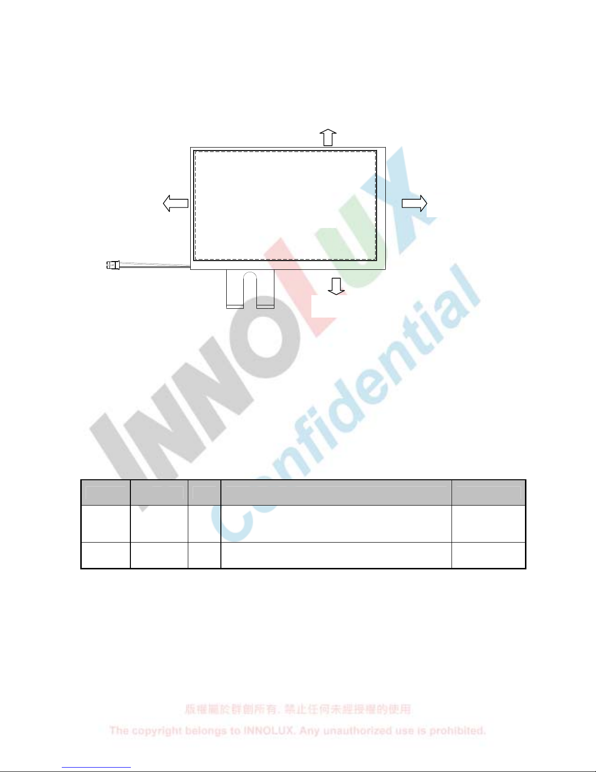
Note 2: Definition of scanning direction.
Refer to the figure as below:
Note 3: When REV=”L”, it’s under normal operation.
When REV=”H”, these data will be inverted.
2.2. Backlight Unit Section
LED Light Bar Connector is used for the integral backlight system.
The recommended model is BHSR-02VS-1 manufactured by JST.
Pin No. Symbol I/O Function Remark
1 V
LED+
P Power for LED backlight anode Pink
2 V
LED-
P Power for LED backlight cathode White
LCM
Left
Right
Up
Down
Page 9

INNOLUX SPEC NO.: A070-84-TT- 12 Date : 2009/02/23
Page : 6/27
The copyright belongs to InnoLux. Any unauthorized use is prohibited.
3. Operation Specifications
3.1. Absolute Maximum Ratings
(Note 2)
Values
Item Symbol
Min. Max.
Unit Remark
DV
DD
-0.5 5 V
AV
DD
-0.5 13.5 V
V
GH
-0.3 20.0 V
V
GL
-13.0 0.3 V
Power voltage
VGH-VGL - 33.0 V
V1~V7
0.4 AVDD AVDD+0.3 V Note 1
Input signal voltage
V8~V14 -0.3 0.6AVDD V
Operation Temperature T
OP
-30 85
℃
Storage Temperature T
ST
-30 85
℃
LED Reverse Voltage Vr - 1.2 V
Each LED
Note 3
LED Forward Current IF - 25 mA Each LED
Note 1: AVDD-0.1≥ V1≥ V2≥ V3≥ V4≥ V5≥ V6≥ V7,
V8≥ V9≥ V10≥ V11≥ V12≥ V13≥ V14≥ AVSS+0.1.
Note 2: The absolute maximum rating values of this product are not allowed to be exceeded
at any times. A module should be used with any of the absolute maximum ratings
exceeded, the characteristics of the module may not be recovered, or in an extreme
condition, the module may be permanently destroyed.
Note 3: Vr Conditions: Zener Diode 20mA
Page 10

INNOLUX SPEC NO.: A070-84-TT- 12 Date : 2009/02/23
Page : 7/27
The copyright belongs to InnoLux. Any unauthorized use is prohibited.
3.2. Typical Operation Conditions
(Note 1)
Values
Item Symbol
Min. Typ. Max.
Unit Remark
DV
DD
3.0 3.3 3.6 V Note 2
AV
DD
10.2 10.4 10.6 V
V
GH
15.3 16.0 16.7 V
Power voltage
V
GL
-7.7 -7.0 -6.3 V
V
COM
3.9 4.1 4.3 V
(V1+V14)/2
=5.2V
V1~V7 0.4 AV
DD
- AVDD -0.1
V
Input signal voltage
V8~V14 0.1 - 0.6 AV
DD
V
Input logic high voltage V
IH
0.7 DV
DD
- DV
DD
V
Input logic low voltage V
IL
0 - 0.3 DV
DD
V
Note 3
Note 1: Be sure to apply DVDD and VGL to the LCD first, and then apply VGH.
Note 2: DV
DD
setting should match the signals output voltage (refer to Note 3) of
customer’s system board.
Note 3: POL, STVD, OEV, CKV, STVU, EDGSL, U/D, STHL, REV, DCLK, STHR, LD, R/L.
R0~R5, G0~G5, B0~B5.
Page 11

INNOLUX SPEC NO.: A070-84-TT- 12 Date : 2009/02/23
Page : 8/27
The copyright belongs to InnoLux. Any unauthorized use is prohibited.
3.2.1. Current Consumption
Values
Item
Symbol
Min. Typ. Max.
Unit
Remark
I
GH
- 0.2 0.5 mA VGH =16.0V
I
GL
- 0.2 1.0 mA VGL = -7.0V
IDV
DD
- 5.0 10.0 mA DVDD =3.3V
Current for Driver
IAV
DD
- 40.0 50.0 mA AVDD =10.4V
3.2.2. Backlight Driving Conditions
Values
Item
Symbol
Min. Typ. Max.
Unit Remark
Voltage for LED Backlight
V
L
9.3 9.9 10.5 V
Note1
Current for LED Backlight
I
L
170 180 200 mA
LED life time - 20,000
- - Hr Note 2
Note 1: The Voltage for LED Backlight is defined at Ta=25℃ and IL =180mA.
Note 2: The “LED life time” is defined as the module brightness decrease to 50% original
brightness at Ta=25℃ and IL =180mA. The LED lifetime could be decreased if
operating IL is larger than 180 mA.
Page 12

INNOLUX SPEC NO.: A070-84-TT- 12 Date : 2009/02/23
Page : 9/27
The copyright belongs to InnoLux. Any unauthorized use is prohibited.
3.3. Power Sequence
1. Power on:
2. Power off:
Note: Data include DCLK,POL,OEV,CKV,STVU,STVD,STHL,STHR,LD,R0~R5,G0~G5,B0~B5
DVDD→→→→VGL→→→→VGH→→→→Data→→→→B/L
B/L→→→→Data→→→→VGH→→→→VGL→→→→DVDD
Page 13

INNOLUX SPEC NO.: A070-84-TT- 12 Date : 2009/02/23
Page : 10/27
The copyright belongs to InnoLux. Any unauthorized use is prohibited.
3.4. Timing Characteristics
3.4.1. Timing Conditions
Values
Item Symbol
Min. Typ. Max.
Unit
Remark
DCLK frequency Fdclk - 40 45 MHz
DCLK cycle Tcph 22 25 - ns
DCLK pulse width Tcw 8 - - ns
Data set-up time Tsu 4 - - ns
Data hold time Thd 2 - - ns
Time that the last data to LD Tld 1 - - Tcph
Pulse width of LD Twld 2 - - Tcph
Time that LD to STHL/R Tlds 5 - - Tcph
POL set-up time Tpsu 6 - - ns
POL hold time Tphd 6 - - ns
CKV frequency Fvclk - - 200 KHz
CKV rise time Trck - - 100 ns
CKV falling time Tfck - - 100 ns
CKV pulse width PWCLK 500 - - ns
Horizontal display timing range
Tdh - 800 - Tcph
Horizontal timing range Th - 1056 - Tcph
STVU/D setup time Tsuv 200 - - ns
STVU/D hold time Thdv 300 - - ns
STVU/D delay time Tdt - - 500 ns
Driver output delay time Tdo - - 900 ns
Page 14

INNOLUX SPEC NO.: A070-84-TT- 12 Date : 2009/02/23
Page : 11/27
The copyright belongs to InnoLux. Any unauthorized use is prohibited.
Output rise time Ttlh - 500 1000 ns
Output falling time Tthl - 400 800 ns
OEV pulse width Twcl 1 - - us
OEV to Driver output delay time Toe - - 900 ns
Horizontal lines per field Tv 512 525 610 Tdh
Vertical display timing range Tvd - 480 - Tdh
Page 15

INNOLUX SPEC NO.: A070-84-TT- 12 Date : 2009/02/23
Page : 12/27
The copyright belongs to InnoLux. Any unauthorized use is prohibited.
3.4.2. Timing Diagram
Tsu Thd
Tcw Tcw
Tsu
Thd
First data Second data Last data
Tphl
Tphl
70%
30%
70%70%
30%30%
70%70%
70%
70%
70%
800
7992
1
DCLK
STHL/R
(input)
STHR/L
(output)
Timing Diagram1 (CHNSL="1" , Default)
<EDGSL="0",Default>
Tcph
70%
Date RGB
Fig.3-1 operation model 1
Page 16

INNOLUX SPEC NO.: A070-84-TT- 12 Date : 2009/02/23
Page : 13/27
The copyright belongs to InnoLux. Any unauthorized use is prohibited.
Tsu Thd
Tcw Tcw
Tsu Thd
First
data
Second
data
Last
data
Tsu
Thd
Tphl
Tphl
70%
30%
70%
30%
30%
70%
30%
70%
30%
30%
70%70%
70%
70%
70%
70%
400
3992
1
DCLK
STHL/R
(input)
Data
RGB
STHR/L
(output)
< EDGSL ="1">
Fig.3-2 operation model 2
Page 17

INNOLUX SPEC NO.: A070-84-TT- 12 Date : 2009/02/23
Page : 14/27
The copyright belongs to InnoLux. Any unauthorized use is prohibited.
DCLK
LD
STHL/R
(input)
LD
POL
Odd
outputs
Even
outputs
70%
Last
Tld
70%
Twld
70%
Tlds
70%
70%
70%
70%
30%
70%
30%
Tpsu Tphd TpsuTphd
High-Z
Tst
10%
90%
High-Z
Tst
90%
10%
70%
Tpsu Tphd
High-Z
Tst
Positive
70%
30%
Negative
Timing Diagram 2
Fig.3-3 Horizontal timing 1
Page 18

INNOLUX SPEC NO.: A070-84-TT- 12 Date : 2009/02/23
Page : 15/27
The copyright belongs to InnoLux. Any unauthorized use is prohibited.
Hs
DCLK
RGB
1 2 3 800799798
DE
Tdh
Th
Fig.3-4 Horizontal timing 2
Page 19

INNOLUX SPEC NO.: A070-84-TT- 12 Date : 2009/02/23
Page : 16/27
The copyright belongs to InnoLux. Any unauthorized use is prohibited.
Fig.3-5 Vertical shift clock timing
Page 20

INNOLUX SPEC NO.: A070-84-TT- 12 Date : 2009/02/23
Page : 17/27
The copyright belongs to InnoLux. Any unauthorized use is prohibited.
Fig.3-6 Vertical timing (from up to down)
Page 21

INNOLUX SPEC NO.: A070-84-TT- 12 Date : 2009/02/23
Page : 18/27
The copyright belongs to InnoLux. Any unauthorized use is prohibited.
RGB
1 2 3 480479478
DE
Vs
Tvd
Tv
Fig.3-7 Vertical timing
Page 22

INNOLUX SPEC NO.: A070-84-TT- 12 Date : 2009/02/23
Page : 19/27
The copyright belongs to InnoLux. Any unauthorized use is prohibited.
4. Optical Specifications
Values
Item Symbol Condition
Min. Typ. Max.
Unit Remark
θ
L
Φ=180°(9 o’clock)
60 70 -
θR Φ=0°(3 o’clock) 60 70 -
θT Φ=90°(12 o’clock)
40 50 -
Viewing angle
(CR≥ 10)
θB Φ=270°(6 o’clock)
60 70 -
degree
Note 1
T
ON
- 10 20 msec Note 3
Response time
T
OFF
- 15 30 msec Note 3
Contrast ratio CR 400 500 - - Note 4
W
X
0.26 0.31 0.36 -
Color chromaticity
W
Y
0.28 0.33 0.38 -
Note 2
Note 5
Note 6
Luminance L 360 450 - cd/m2 Note 6
Luminance uniformity
Y
U
Normal
θ=Φ=0°
70 75 - % Note 7
Test Conditions:
1. DVDD =3.3V, IL =180mA (Backlight current), the ambient temperature is 25℃.
2. The test systems refer to Note 2.
Page 23

INNOLUX SPEC NO.: A070-84-TT- 12 Date : 2009/02/23
Page : 20/27
The copyright belongs to InnoLux. Any unauthorized use is prohibited.
Note 1: Definition of viewing angle range
Fig. 4-1 Definition of viewing angle
Note 2: Definition of optical measurement system.
The optical characteristics should be measured in dark room. After 30 minutes
operation, the optical properties are measured at the center point of the LCD
screen. (Response time is measured by Photo detector TOPCON BM-7, other
items are measured by BM-5A/Field of view: 1° /Height: 500mm.)
Fig. 4-2 Optical measurement system setup
Normal line
θ=Φ=0°
Φ=90°
12 o’clock direction
Φ=270°
6 o’clock direction
Φ=0°
Φ=180°
Active Area
θ
L
θ
T
θ
B
θ
R
Normal line
θ=Φ=0°
Photo detector
Φ=90°
12 o’clock direction
Φ=0° Φ=180°
500mm
LCM
Φ=270°
6 o’clock direction
LCM
Page 24

INNOLUX SPEC NO.: A070-84-TT- 12 Date : 2009/02/23
Page : 21/27
The copyright belongs to InnoLux. Any unauthorized use is prohibited.
Note 3: Definition of Response time
The response time is defined as the LCD optical switching time interval between
“White” state and “Black” state. Rise time (TON) is the time between photo detector
output intensity changed from 90% to 10%. And fall time (T
OFF
) is the time
between photo detector output intensity changed from 10% to 90%.
Fig. 4-3 Definition of response time
Note 4: Definition of contrast ratio
state Black"" the on LCD whenmeasured Luminance
state White"" the on LCD whenmeasured Luminance
(CR) ratio Contrast =
Note 5: Definition of color chromaticity (CIE1931)
Color coordinates measured at center point of LCD.
Note 6: All input terminals LCD panel must be ground while measuring the center area of
the panel. The LED driving condition is IL=180mA .
100%
90%
10%
0%
Photo detector output
(Relative value)
T
ON
T
OFF
White (TFT OFF)
Black (TFT ON)
White (TFT OFF)
Page 25

INNOLUX SPEC NO.: A070-84-TT- 12 Date : 2009/02/23
Page : 22/27
The copyright belongs to InnoLux. Any unauthorized use is prohibited.
Note 7: Definition of Luminance Uniformity
Active area is divided into 9 measuring areas (Refer to Fig. 4-4 ).Every measuring
point is placed at the center of each measuring area.
max
min
B
B
(Yu)Uniformity Luminance =
L-------Active area length W----- Active area width
W
W/3
W/3
W/6
L/3
L/3
L/6
L
Fig. 4-4 Definition of measuring points
B
max
: The measured maximum luminance of all measurement position.
B
min
: The measured minimum luminance of all measurement position.
Page 26

INNOLUX SPEC NO.: A070-84-TT- 12 Date : 2009/02/23
Page : 23/27
The copyright belongs to InnoLux. Any unauthorized use is prohibited.
5. Reliability Test Items
(Note3)
Item Test Conditions Remark
High Temperature Storage
Ta = 85℃ 240 hrs
Note 1,Note 4
Low Temperature Storage
Ta = -30℃ 240hrs
Note 1,Note 4
High Temperature Operation
Ts = 85℃ 240hrs
Note 2,Note 4
Low Temperature Operation
Ta =-30℃ 240hrs
Note 1,Note 4
Operate at High Temperature
and Humidity
+60℃, 90%RH max. 240 hrs
Note 4
Thermal Shock
-30℃/30 min ~ +85℃/30 min for a total 100
cycles, Start with cold temperature and end
with high temperature
Note 4
Vibration Test
Frequency range:10~55Hz
Stroke:1.5mm
Sweep:10Hz~55Hz~10Hz
2 hours for each direction of X. Y. Z.
(6 hours for total)
Mechanical Shock
100G 6ms,±X, ±Y, ±Z 3 times for each
direction
Package Vibration Test
Random Vibration :
0.015G*G/Hz from 5-200HZ, -6dB/Octave
from 200-500HZ
2 hours for each direction of X. Y. Z.
(6 hours for total)
Package Drop Test
Height:60 cm
1 corner, 3 edges, 6 surfaces
Electro Static Discharge ± 2KV, Human Body Mode, 100pF/1500Ω
Note 1: Ta is the ambient temperature of samples.
Note 2: Ts is the temperature of panel’s surface.
Note 3: In the standard condition, there shall be no practical problem that may affect the
display function. After the reliability test, the product only guarantees operation,
but doesn’t guarantee all the cosmetic specification.
Note 4: Before cosmetic and function test, the product must have enough recovery time,
at least 2 hours at room temperature.
Page 27

INNOLUX SPEC NO.: A070-84-TT- 12 Date : 2009/02/23
Page : 24/27
The copyright belongs to InnoLux. Any unauthorized use is prohibited.
6. General Precautions
6.1. Safety
Liquid crystal is poisonous. Do not put it in your mouth. If liquid crystal touches your
skin or clothes, wash it off immediately by using soap and water.
6.2. Handling
1. The LCD panel is plate glass. Do not subject the panel to mechanical shock or to
excessive force on its surface.
2. The polarizer attached to the display is easily damaged. Please handle it carefully
to avoid scratch or other damages.
3. To avoid contamination on the display surface, do not touch the module surface
with bare hands.
4. Keep a space so that the LCD panels do not touch other components.
5. Put cover board such as acrylic board on the surface of LCD panel to protect panel
from damages.
6. Transparent electrodes may be disconnected if you use the LCD panel under
environmental conditions where the condensation of dew occurs.
7. Do not leave module in direct sunlight to avoid malfunction of the ICs.
6.3. Static Electricity
1. Be sure to ground module before turning on power or operating module.
2. Do not apply voltage which exceeds the absolute maximum rating value.
6.4. Storage
1. Store the module in a dark room where must keep at 25±10℃ and 65%RH or less.
2. Do not store the module in surroundings containing organic solvent or corrosive
gas.
3. Store the module in an anti-electrostatic container or bag.
6.5. Cleaning
1. Do not wipe the polarizer with dry cloth. It might cause scratch.
2. Only use a soft sloth with IPA to wipe the polarizer, other chemicals might
permanent damage to the polarizer.
Page 28

INNOLUX SPEC NO.: A070-84-TT- 12 Date : 2009/02/23
Page : 25/27
The copyright belongs to InnoLux. Any unauthorized use is prohibited.
7. Mechanical Drawing
Page 29

INNOLUX SPEC NO.: A070-84-TT- 12 Date : 2009/02/23
Page : 26/27
The copyright belongs to InnoLux. Any unauthorized use is prohibited.
8. Package Drawing
8.1. Packaging Material Table
No. Item
Model
(Material)
Dimensions(mm)
Unit
Weight
(kg)
Quantity Remark
1
LCM
Module
AT070TN84 V.1 165 × 104 × 5.5 0.170 50 pcs
2 Partition
BC Corrugated
Paper
512 × 349 × 226 1.466 1 set
3
Corrugated
Bar
BC Corrugated
Paper
512 × 162 0.046 4 set
4
Corrugated
Board
BC Corrugated
Paper
510 × 343 0.130 1 pcs
5
Dust-Proof
Bag
PE 700 × 530 0.048 1 pcs
6 A/S Bag PE 180 × 160 × 0.05 0.002 50 pcs
7 Carton
Corrugated
paper
530 × 355 × 255 1.100 1 pcs
8 Total weight
11. 52 8 Kg ±5 %
8.2. Packaging Quantity
Total LCM quantity in Carton: no. of Partition 2 Rows x quantity per Row 25 = 50
Page 30

INNOLUX SPEC NO.: A070-84-TT- 12 Date : 2009/02/23
Page : 27/27
The copyright belongs to InnoLux. Any unauthorized use is prohibited.
8.3. Packaging Drawing
 Loading...