

infneon XC164CS Data Sheet

Data Sheet, V2.1, Jun. 2003
XC164CS
16-Bit Single-Chip Microcontroller
Microcontrollers
Never stop thinking.

Edition 2003-06
Published by Infineon Technologies AG,
St.-Martin-Strasse 53,
D-81541 München, Germany
© Infineon Technologies AG 2003.
All Rights Reserved.
Attention please!
The information herein is given to describe certain components and shall not be considered as warranted
characteristics.
Terms of delivery and rights to technical change reserved.
We hereby disclaim any and all warranties, including but not limited to warranties of non-infringement, regarding
circuits, descriptions and charts stated herein.
Information
For further information on technology, delivery terms and conditions and prices please contact your nearest
Infineon Technologies Office in Germany or our Infineon Technologies Representatives worldwide (see address
list).
Warnings
Due to technical requirements components may contain dangerous substances. For information on the types in
question please contact your nearest Infineon Technologies Office.
Infineon Technologies Components may only be used in life-support devices or systems with the express written
approv al of Infine on T ec hnologies , if a failu re of such co mponents ca n reasonab ly be exp ected to cause the f ailu re
of that lif e-s upport device or sys tem, or to affect the sa f ety or ef f ec tiveness of that device or sy ste m. Life support
devices or systems are intended to be implanted in the human body, or to support and/or maintain and sustain
and/or protect human life. If they fail, it is reasonable to assume that the health of the user or other persons may
be endangered.

Data Sheet, V2.1, Jun. 2003
XC164CS
16-Bit Single-Chip Microcontroller
Microcontrollers
Never stop thinking.

XC164
Revision History: 2003-06 V2.1
Previous Version: 2003-01 V2.0
2002-03 V1.0
Page Subjects (major changes since last revision)
1 AD conversion times updated
6, 45 RSTIN note added
45 Digital supply voltage range for IO pads improved
48 Note 2 added
49ff Specification of Sleep and Power-down mode supply current improved
53 Conversion time formulas improved
54 Note 4 changed
55 Converter timing example improved
58 Note 1 added
63 Table 19 changed
Controller Area Network (CAN): License of Robert Bosch GmbH
We Listen to Your Comments
Any information within this document that you feel is wrong, unclear or missing at all?
Your feedback will help us to continuously improve the quality of this document.
Please send your proposal (including a reference to this document) to:
mcdocu.comments@infineon.com

XC16416-Bit Single-Chip Microcontroller
XC166 Family
XC164
1 Summary of Features
• High Performance 16-bit CPU with 5-Stage Pipeline
– 25 ns Instruction Cycle Time at 40 MHz CPU Clock (Single-Cycle Execution)
– 1-Cycle Multiplication (16 × 16 bit), Background Division (32 / 16 bit) in 21 Cycles
– 1-Cycle Multiply-and-Accumulate (MAC) Instructions
– Enhanced Boolean Bit Manipulation Facilities
– Zero-Cycle Jump Execution
– Additional Instructions to Support HLL and Operating Systems
– Register-Based Design with Multiple Variable Register Banks
– Fast Context Switching Support with Two Additional Local Register Banks
– 16 Mbytes Total Linear Address Space for Code and Data
– 1024 Bytes On-Chip Special Function Register Area (C166 Family Compatible)
• 16-Priority-Level Interr upt S ystem with u p to 75 Sources, Sample- Rate down to 50 ns
• 8-Channel Interrupt-Driven Single-Cycle Data Transfer Facilities via
Peripheral Event Controller (PEC), 24-Bit Pointers Cover Total Address Space
• Clock Generation via on-chip PLL (factors 1:0.15 … 1:10), or
via Prescaler (factors 1:1 … 60:1)
• On-Chip Memory Modules
– 2 Kbytes On-Chip Dual-Port RAM (DPRAM)
– 2 Kbytes On-Chip Data SRAM (DSRAM)
– 2 Kbytes On-Chip Program/Data SRAM (PSRAM)
– 128 Kbytes On-Chip Program Memory (Flash Memory or Mask ROM)
• On-Chip Peripheral Modules
– 14-Channel A/D Converter with Programmable Resolution (10-bit or 8-bit) and
Conversion Time (down to 2.55 µs or 2.15 µs)
– Two 16-Channel General Purpose Capture/Compare Units (12 Input/Output Pins)
– Capture/Compare Unit for flexible PWM Signal Generation (CAPCOM6)
(3/6 Capture/Compare Channels and 1 Compare Channel)
– Multi-Functional General Purpose Timer Unit with 5 Timers
– Two Synchronous/Asynchronous Serial Channels (USARTs)
– Two High-Speed-Synchronous Serial Channels
– On-Chip TwinCAN Interface (Rev. 2.0B active) with 32 Message Objects
(Full CAN/Basic CAN) on Two CAN Nodes, and Gateway Functionality
– On-Chip Real Time Clock
• Idle, Sleep, and Power Down Modes with Flexible Power Management
• Programmable Watchdog Timer and Oscillator Watchdog
Data Sheet 1 V2.1, 2003-06

XC164
Derivatives
• Up to 12 Mbytes External Address Space for Code and Data
– Programmable External Bus Characteristics for Different Address Ranges
– Multiplexed or Demultiplexed External Address/Data Buses
– Selectable Address Bus Width
– 16-Bit or 8-Bit Data Bus Width
– Four Programmable Chip-Select Signals
• Up to 79 General Purpose I/O Lines,
partly with Selectable Input Thresholds and Hysteresis
• On-Chip Bootstrap Loader
• Supported by a Large Range of Development Tools like C-Compilers,
Macro-Assembler Packages, Emulators, Evaluation Boards, HLL-Debuggers,
Simulators, Logic Analyzer Disassemblers, Programming Boards
• On-Chip Debug Support via JTAG Interface
• 100-Pin TQFP Package, 0.5 mm (19.7 mil) pitch
Ordering Information
The ordering code for Infineon microcontrollers provides an exact reference to the
required product. This ordering code identifies:
Summary of Features
• the derivative itself, i.e. its function set, the temper ature range, and the supp ly voltage
• the package and the type of delivery.
For the available ordering codes for the XC164 please refer to the “Product Catalog
Microcontrollers”, which summarizes all available microcontroller variants.
Note: The ordering codes for Mask-ROM versions are defined for each product after
verification of the respective ROM code.
This document describes several derivatives of the XC164 group. Table 1 enumerates
these derivatives and summ arizes the differences. As this document r efers to all of these
derivatives, some descriptions may not apply to a specific product.
For simplicity all versions are referred to by the term XC164 throughout this document.
Data Sheet 2 V2.1, 2003-06
XC164
Derivatives
Table 1 XC164 Derivative Synopsis
Derivative
SAK-XC164CS-16F40F,
1)
Program Memory On-Chip RAM Interfaces
128 Kbytes Flash 2 Kbytes DPRAM,
SAK-XC164CS-16F20F
SAK-XC164CS-16R40F,
128 Kbytes ROM 2 Kbytes DPRAM,
SAK-XC164CS-16R20F
SAF-XC164CS-16F40F,
128 Kbytes Flash 2 Kbytes DPRAM,
SAF-XC164CS-16F20F
SAF-XC164CS-16R40F,
128 Kbytes ROM 2 Kbytes DPRAM,
SAF-XC164CS-16R20F
SAK-XC164CS-8F40F,
64 Kbytes Flash 2 Kbytes DPRAM,
SAK-XC164CS-8F20F
Summary of Features
2 Kbytes DSRAM,
2 Kbytes PSRAM
2 Kbytes DSRAM,
2 Kbytes PSRAM
2 Kbytes DSRAM,
2 Kbytes PSRAM
2 Kbytes DSRAM,
2 Kbytes PSRAM
2 Kbytes DSRAM,
2 Kbytes PSRAM
ASC0, ASC1,
SSC0, SSC1,
CAN0, CAN1
ASC0, ASC1,
SSC0, SSC1,
CAN0, CAN1
ASC0, ASC1,
SSC0, SSC1,
CAN0, CAN1
ASC0, ASC1,
SSC0, SSC1,
CAN0, CAN1
ASC0, ASC1,
SSC0, SSC1,
CAN0, CAN1
SAK-XC164CS-8R40F,
SAK-XC164CS-8R20F
SAF-XC164CS-8F40F,
SAF-XC164CS-8F20F
SAF-XC164CS-8R40F,
SAF-XC164CS-8R20F
1)
This Data Sheet i s vali d for de vices starting with a nd incl uding de sign st ep AD of th e Flash v ersion , and design
step AA of the ROM version.
64 Kbytes ROM 2 Kbytes DPRAM,
2 Kbytes DSRAM,
2 Kbytes PSRAM
64 Kbytes Flash 2 Kbytes DPRAM,
2 Kbytes DSRAM,
2 Kbytes PSRAM
64 Kbytes ROM 2 Kbytes DPRAM,
2 Kbytes DSRAM,
2 Kbytes PSRAM
ASC0, ASC1,
SSC0, SSC1,
CAN0, CAN1
ASC0, ASC1,
SSC0, SSC1,
CAN0, CAN1
ASC0, ASC1,
SSC0, SSC1,
CAN0, CAN1
Data Sheet 3 V2.1, 2003-06
XC164
Derivatives
General Device Information
2 General Device Informati o n
2.1 Introduction
The XC164 derivatives are high-performance m embers of the Infineon X C166 Family of
full featured single-chip CMOS microcontrollers. These devices extend the functionality
and performan ce of the C166 Family in terms of instructions (MA C unit), periphe rals, and
speed. They combine high CPU performance (up to 40 million instructions per second)
with high peripheral functionality and enhanced IO-capabilities. They also provide clock
generation via PLL and various on-chip memory modules such as program ROM or
Flash, program RAM, and data RAM.
AGND
V
DDI/P
V
SSI/P
PORT0
16 bit
XTAL1
XTAL2
V
AREF
V
Port 20
5 bit
NMI
RSTIN
RSTOUT
EA
ALE
RD
WR/WRL
Port 5
14 bit
XC164
TRST JTAG Debug
PORT1
16 bit
Port 3
14 bit
Port 4
8 bit
Port 9
6 bit
Via Port 3
Figure 1 Logi c Symbol
Data Sheet 4 V2.1, 2003-06
XC164
Derivatives
General Device Information
2.2 Pin Configuration and Definition
The pins of the XC164 are described in detail in Table 2, including all their alternate
functions. Figure 2 summarizes all pins in a condensed way, showing their location on
the 4 sides of the package. E*) and C*) mark pins to be used as alternate external
interrupt inputs, C*) marks pins that can have CAN interface lines assigned to them.
/MTSR1/EX2IN
/CC23/EX0I N
RSTIN
P20.12/RSTOUT
NMI
P0H.0/ AD8
P0H.1/ AD9
P0H.2/AD10
P0H.3/AD11
V
SSP
V
P9.0/CC16IO/C*)
P9.1/CC17IO/C*)
P9.2/CC18IO/C*)
P9.3/CC19IO/C*)
P9.4/CC20I O
P9.5/CC21I O
P5.10/AN10/T6EUD
P5.11/AN11/T5EUD
DDP
V
SSP
V
DDP
P5.0/AN0
P5.1/AN1
P5.2/AN2
P5.3/AN3
P5.4/AN4
P5.5/AN5
6P1/MRST1/ EX1I N
SSIVDDI
XTAL1
XTAL2
V
P1H.7/A15/CC27/EX7IN
P1H.6/A14/CC26/EX6IN
P1H.5/A13/CC25/EX5IN
P1H.4/A12/CC24/EX4IN
P1H.3/A11/T7IN/SCLK1/EX3IN/E*)
100999897969594939291908988878685848382818079787776
1
2
3
4
5
6
7
8
9
10
11
12
13
14
15
16
17
18
19
20
21
22
23
24
25
P1H.0/A8/C6P0
P1H.2/A10/C6P2
P1H.1/A9/C
XC164
SSPVDDP
V
TRAP/CC22
C
P1L.6/A6/COUT63
P1L.5/A5/COUT62
P1L.4/A4/CC62
P1L.3/A3/COUT61
P1L.2/A2/CC61
P1L.1/A1/COUT60
P1L.0/A0/CC60
P0H.7/AD15
P0H.6/AD14
P1L.7/A7/
P0H.5/AD13
75
P0H.4/ AD1 2
74
P0L.7/A D7
73
P0L.6/A D6
72
P0L.5/A D5
71
P0L.4/A D4
70
P0L.3/A D3
69
P0L.2/A D2
68
P0L.1/A D1
67
P0L.0/A D0
66
P20.5/E A
65
P20.4/A LE
64
P20.1/WR
63
P20.0/R D
62
V
61
V
60
P4.7/A23 /C*)
59
P4.6/A22 /C*)
58
P4.5/A21/C*)
57
P4.4/A20/C*)
56
P4.3/A19 /CS0
55
P4.2/A18 /CS1
54
P4.1/A17 /CS2
53
P4.0/A16 /CS3
52
P3.15/C LKOUT /FO
51
P3.13/SCLK0/E*)
/WRL
SSP
DDP
26272829303132333435363738394041424344454647484950
SSI
DDI
SSP
TRST
DDP
V
V
P3.6/T3I N
P3.8/MRST0
P3.9/MTS R0
P3.2/CAP IN/TD I
P3.3/T3OUT/TDO
P3.4/T3EUD/TMS
P3.1/T6OUT/ RxD 1/TC K/ E* )
P3.7/T2IN/BRKIN
P3.5/ T4 I N/TxD1/BRKOUT
/WRH/E*)
P3.10/TxD0/E*)
P3.11/RxD0/E*)
P3.12/BHE
V
AREF
AGND
V
P5.6/AN6
V
P5.7/AN7
P5.12/AN12/T6IN
P5.13/AN13/T5IN
P5.14/AN14/T4EUD
V
P5.15/AN15/T2EUD
Figure 2 Pin Configuration (top view)
Data Sheet 5 V2.1, 2003-06
XC164
Derivatives
Table 2 Pin Definitions and Functions
Symbol Pin
Num.
RSTIN 1 I Reset Input with Schmitt-Trigger characteristics. A low level
Input
Outp.
Function
at this pin while the oscillator is running resets the XC164.
A spike filter suppresses input pulses <10 ns. Input pulses
>100 ns safely pass the filter. The minimum duration for a
safe recognition should be 100 ns + 2 CPU clock cycles.
General Device Information
Note: The reset duration must be sufficient to let the
hardware configuration signals settle.
External circuitry must guarantee low level at the
RSTIN pin at least until both power supply voltages
have reached the operating range.
P20.12 2 IO For details, please refer to the description of P20.
NMI 3 I Non-Maskable Interrupt Input. A high to low transition at this
pin causes the CPU to vector to the NMI trap routine. When
the PWRDN (power down) instruction is executed , the NM I
pin must be low i n order to force the XC164 into power down
mode. If NMI is high, when PWRDN is executed, the part will
continue to run in normal mode.
If not used, pin NMI should be pulled high externally.
P0H.0P0H.3
4…7 IO For details, please refer to the description of PORT0.
Data Sheet 6 V2.1, 2003-06
XC164
Derivatives
Table 2 Pin Definitions and Functions (cont’d)
Symbol Pin
Num.
P9
Input
Outp.
IO
Function
Port 9 is a 6-bit bidirectional I/O port. Each pin can be
programmed for input (output driver in high-impedance
state) or output (configurable as push/pull or open drain
driver). The input threshold of Port 9 is selectable (standard
or special).
The following Port 9 pins also serve for alternate functions:
P9.0
P9.1
P9.2
P9.3
P9.4
P9.5
10
11
12
13
14
15
I/O
I
I
I/O
O
I
I/O
I
I
I/O
O
I
I/O
I/O
CC16IO CAPCOM2: CC16 Capture Inp./Compare Outp.,
CAN2_RxDCAN Node 2 Receive Data Input,
EX7IN Fast External Interrupt 7 Input (alternate pin B)
CC17IO CAPCOM2: CC17 Capture Inp./Compare Outp.,
CAN2_TxD CAN Node 2 Transmit Data Output,
EX6IN Fast External Interrupt 6 Input (alternate pin B)
CC18IO CAPCOM2: CC18 Capture Inp./Compare Outp.,
CAN1_RxDCAN Node 1 Receive Data Input,
EX7IN Fast External Interrupt 7 Input (alternate pin A)
CC19IO CAPCOM2: CC19 Capture Inp./Compare Outp.,
CAN1_TxD CAN Node 1 Transmit Data Output,
EX6IN Fast External Interrupt 6 Input (alternate pin A)
CC20IO CAPCOM2: CC20 Capture Inp./Compare Outp.
CC21IO CAPCOM2: CC21 Capture Inp./Compare Outp.
General Device Information
1)
P5
P5.0
P5.1
P5.2
P5.3
P5.4
P5.5
P5.10
P5.11
P5.6
P5.7
P5.12
P5.13
P5.14
P5.15
18
19
20
21
22
23
24
25
26
27
30
31
32
33
I
Port 5 is a 14-bit input-only port.
The pins of Port 5 also serve as anal og input channels for the
A/D converter, or they serve as timer inputs:
I
I
I
I
I
I
I
I
I
I
I
I
I
I
AN0
AN1
AN2
AN3
AN4
AN5
AN10, T6EUD GPT2 Timer T6 Ext. Up/Down C trl. Inp.
AN11, T5EUD GPT2 Timer T5 Ext. Up/Down C trl. Inp.
AN6
AN7
AN12, T6IN GPT2 Timer T6 Count/Gate Input
AN13, T5IN GPT2 Timer T5 Count/Gate Input
AN14, T4EUD GPT1 Timer T4 Ext. Up/Down C trl. Inp.
AN15, T2EUD GPT1 Timer T2 Ext. Up/Down C trl. Inp.
Data Sheet 7 V2.1, 2003-06
XC164
Derivatives
Table 2 Pin Definitions and Functions (cont’d)
Symbol Pin
Num.
TRST 36 I Test-System Reset Input. A high level at this pin activates
P3
P3.1
P3.2
P3.3
P3.4
P3.5
P3.6
P3.7
P3.8
P3.9
P3.10
P3.11
P3.12
P3.13
P3.15
39
40
41
42
43
44
45
46
47
48
49
50
51
52
Input
Outp.
IO
O
I/O
I
I
I
I
O
O
I
I
I
O
O
I
I
I
I/O
I/O
O
I
I/O
I
O
O
I
I/O
I
O
O
Function
the XC164’s debug system. For normal system operation,
pin TRST should be held low.
Port 3 is a 14-bit bidirectional I/O port. Each pin can be
programmed for input (output driver in high-impedance
state) or output (configurable as push/pull or open drain
driver). The input threshold of Port 3 is selectable (standard
or special).
The following Port 3 pins also serve for alternate functions:
T6OUT GPT2 Timer T6 Toggle Latch Output,
RxD1 ASC1 Data Input (Async.) or Inp./Outp. (Sync.),
EX1IN Fast External Interrupt 1 Input (alternate pin A),
TCK Debug System: JTAG Clock Input
CAPIN GPT2 Register CAPREL Capture Input,
TDI Debug System: JTAG Data In
T3OUT GPT1 Timer T3 Toggle Latch Output,
TDO Debug System: JTAG Data Out
T3EUD GPT1 Timer T3 External Up/D own Control Input,
TMS Debug System: JTAG Test Mode Selection
T4IN GPT1 Timer T4 Count/Gate/Reload/Capture Inp
TxD1 ASC0 Clock/Data Output (Async./Sync.),
BRKOUT Debug System: Break Out
T3IN GPT1 Timer T3 Count/Gate Input
T2IN GPT1 Timer T2 Count/Gate/Reload/Capture Inp
BRKIN Debug System: Break In
MRST0 SSC0 Master-Receive/Slave-Transmit In/Out.
MTSR0 SSC0 Master-Transmit/Slave-Receive Out/In.
TxD0 ASC0 Clock/Data Output (Async./Sync.),
EX2IN Fast External Interrupt 2 Input (alternate pin B)
RxD0 ASC0 Data Input (Async.) or Inp./Outp. (Sync.),
EX2IN Fast External Interrupt 2 Input (alternate pin A)
BHE External Memory High Byte Enable Signal,
WRH External Memory High Byte Write Strobe,
EX3IN Fast External Interrupt 3 Input (alternate pin B)
SCLK0 SSC0 Master Clock Output / Slave Clock Input.,
EX3IN Fast External Interrupt 3 Input (alternate pin A)
CLKOUT System Clock Output (=CPU Clock),
FOUT Programmable Frequency Output
General Device Information
Data Sheet 8 V2.1, 2003-06
XC164
Derivatives
Table 2 Pin Definitions and Functions (cont’d)
Symbol Pin
Num.
P4
Input
Outp.
IO
Function
Port 4 is an 8-bit bidirectional I/O port. Each pin can be
programmed for input (output driver in high-impedance
state) or output (configurable as push/pull or open drain
driver). The input threshold of Port 4 is selectable (standard
or special).
Port 4 can be used to output the segment address lines, the
optional chip select lines, and for serial interface lines:
P4.0
P4.1
P4.2
P4.3
P4.4
P4.5
P4.6
P4.7
53
54
55
56
57
58
59
60
O
O
O
O
O
O
O
O
O
I
I
O
I
I
O
O
I
O
I
O
I
A16 Least Significant Segment Address Line,
CS3 Chip Select 3 Output
A17 Segment Address Line,
CS2 Chip Select 2 Output
A18 Segment Address Line,
CS1 Chip Select 1 Output
A19 Segment Address Line,
CS0 Chip Select 0 Output
A20 Segment Address Line,
CAN2_RxDCAN Node 2 Receive Data Input,
EX5IN Fast External Interrupt 5 Input (alternate pin B)
A21 Segment Address Line,
CAN1_RxDCAN Node 1 Receive Data Input,
EX4IN Fast External Interrupt 4 Input (alternate pin B)
A22 Segment Address Line,
CAN1_TxD CAN Node 1 Transmit Data Output,
EX5IN Fast External Interrupt 5 Input (alternate pin A)
A23 Most Significant Segment Address Line,
CAN1_RxDCAN Node 1 Receive Data Input,
CAN2_TxD CAN Node 2 Transmit Data Output,
EX4IN Fast External Interrupt 4 Input (alternate pin A)
General Device Information
1)
Data Sheet 9 V2.1, 2003-06
XC164
Derivatives
Table 2 Pin Definitions and Functions (cont’d)
Symbol Pin
Num.
P20
P20.0
P20.1
P20.4
P20.5
P20.12
63
64
65
66
2
Input
Outp.
IO
O
O
O
I
O
Function
Port 20 is a 6-bit bidirectional I/O port. Each pin can be
programmed for input (output driver in high-impedance
state) or output. The input threshold of Port 20 is selectable
(standard or special).
The following Port 20 pins also serve for alternate functions:
RD External Memory Read Strobe, activated for
every external instruction or data read access.
WR/WRL External Memory Write Strobe.
In WR-mode this pin is activated for every
external data write access.
In WRL-mode this pin is activated for low byte
data write accesses on a 16-bit bus, and for
every data write access on an 8-bit bus.
ALE Address Latch Enable Output.
Can be used for latching the address into
external memory or an address latch in the
multiplexed bus modes.
EA External Access Enable pin.
A low level at this pin during and after Reset
forces the XC164 to latch the configuration fr om
PORT0 and pin RD, and to begin instruction
execution out of external memory.
A high level forces the XC164 to latch the
configuration from pins RD, ALE, and WR, and
to begin instruction execution out of the internal
program memory. "ROMless" versions must
have this pin tied to ‘0’.
RSTOUT Internal Reset Indication Output.
Is activated asynchronously with an external
hardware reset. It may also be activated
(selectable) synchronously with an internal
software or watchdog reset.
Is deactivated upon the execution of the EINIT
instruction, optionally at the end of reset, or at
any time (before EINIT) via user software.
General Device Information
Note: Port 20 pins may input configuration values (see EA).
Data Sheet 10 V2.1, 2003-06
XC164
Derivatives
Table 2 Pin Definitions and Functions (cont’d)
Symbol Pin
Num.
PORT0
P0L.0-7
P0H.0-3
P0H.4-7
67 - 74
4 - 7
75 - 78
Input
Outp.
IO PORT0 consists of the two 8-bit bidirectional I/O ports P0L
Function
and P0H. Each pin can be programmed for input (output
driver in high-impedance state) or output.
In case of an external bus configuration, PORT0 serves as
the address (A) and address/data (AD) bus in multiplexed
bus modes and as the data (D) bus in demultiplexed bus
modes.
Demultiplexed bus modes:
Data Path Width: 8-bit 16-bit
P0L.0 – P0L.7: D0 – D7 D0 - D7
P0H.0 – P0H.7: I/O D8 - D15
Multiplexed bus modes:
Data Path Width: 8-bit 16-bit
P0L.0 – P0L.7: AD0 – AD7 AD0 - AD7
P0H.0 – P0H.7: A8 - A15 AD8 - AD15
General Device Information
PORT1
P1L.0
P1L.1
P1L.2
P1L.3
P1L.4
P1L.5
P1L.6
P1L.7
P1H
79
80
81
82
83
84
85
86
…
IO
I/O
O
I/O
O
I/O
O
O
I
I/O
Note: At the end of an external reset (EA = 0) PORT0 also
may input configuration values
PORT1 consists of the two 8-bit bidirectional I/O ports P1L
and P1H. Each pin can be programmed for input (output
driver in high-impedance state) or output.
PORT1 is used as the 16-bit address bus (A) in
demultiplexed bus modes (also after switching from a
demultiplexed to a multiplexed bus mode).
The following PORT1 pins also serve for alt. functions:
CC60 CAPCOM6: Input / Output of Channel 0
COUT60 CAPCOM6: Output of Channel 0
CC61 CAPCOM6: Input / Output of Channel 1
COUT61 CAPCOM6: Output of Channel 1
CC62 CAPCOM6: Input / Output of Channel 2
COUT62 CAPCOM6: Output of Channel 2
COUT63 Output of 10-bit Compare Channel
CTRAP CAPCOM6: Trap Input
CTRAP is an input pin with an internal pullup resistor. A low
level on this pin switches the CAPCOM6 compare outputs to
the logic level defined by software (if enabled).
CC22IO CAPCOM2: CC22 Capture Inp./Compare Outp.
…continued…
Data Sheet 11 V2.1, 2003-06
XC164
Derivatives
Table 2 Pin Definitions and Functions (cont’d)
Symbol Pin
Num.
PORT1
Input
Outp.
IO
Function
…continued…
(cont’d)
P1H.0
P1H.1
P1H.2
P1H.3
P1H.4
P1H.5
P1H.6
P1H.7
89
90
91
92
93
94
95
96
I
I
I/O
I
I
I/O
I
I
I/O
I
I/O
I
I
I/O
I
I/O
I
I/O
I
I/O
I
CC6POS0 CAPCOM6: Position 0 Input,
EX0IN Fast External Interrupt 0 Input (default pin),
CC23IO CAPCOM2: CC23 Capture Inp./Compare Outp.
CC6POS1 CAPCOM6: Position 1 Input,
EX1IN Fast External Interrupt 1 Input (default pin),
MRST1 SSC1 Master-Receive/Slave-Transmit In/Out.
CC6POS2 CAPCOM6: Position 2 Input,
EX2IN Fast External Interrupt 2 Input (default pin),
MTSR1 SSC1 Master-Transmit/Slave-Receive Out/Inp.
T7IN CAPCOM2: Timer T7 Count Input,
SCLK1 SSC1 Master Clock Output / Slave Clock Input,
EX3IN Fast External Interrupt 3 Input (default pin),
EX0IN Fast External Interrupt 0 Input (alternate pin A)
CC24IO CAPCOM2: CC24 Capture Inp./Compare Outp.,
EX4IN Fast External Interrupt 4 Input (default pin)
CC25IO CAPCOM2: CC25 Capture Inp./Compare Outp.,
EX5IN Fast External Interrupt 5 Input (default pin)
CC26IO CAPCOM2: CC26 Capture Inp./Compare Outp.,
EX6IN Fast External Interrupt 6 Input (default pin)
CC27IO CAPCOM2: CC27 Capture Inp./Compare Outp.,
EX7IN Fast External Interrupt 7 Input (default pin)
General Device Information
XTAL2
XTAL199100
O
I
XTAL2: Output of the oscillator amplifier circuit
XTAL1: Input to the oscillator amplifier and input to
the internal clock generator
To clock the device from an external source, drive XTAL1,
while leaving XTAL2 unconnected. Minimum and maximum
high/low and rise/fall times specified in the AC
Characteristics must be observed.
V
AREF
V
AGND
V
DDI
28 - Reference voltage for the A/D converter.
29 - Reference ground for the A/D converter.
35, 97 - Digital Core Supply Voltage (On-Chip Modules):
+2.5 V during normal operation and idle mode.
Please refer to the Operating Conditions
Data Sheet 12 V2.1, 2003-06
XC164
Derivatives
General Device Information
Table 2 Pin Definitions and Functions (cont’d)
Symbol Pin
Num.
V
DDP
9, 17,
38, 61,
87
V
V
SSI
SSP
34, 98 - Digital Ground.
8, 16,
37, 62,
88
Input
Function
Outp.
- Digital Pad Supply Voltage (Pin Output Drivers):
+5 V during normal operation and idle mode.
Please refer to the Operating Conditions
-
Connect decoupling capacitors to adjacent VDD/VSS pin
pairs as close as possible to the pins.
All VSS pins must be connected to the gro und-line o r groundplane.
1)
The CAN interface lines are assigned to ports P4 and P9 under software control.
Data Sheet 13 V2.1, 2003-06
XC164
Derivatives
Functional Description
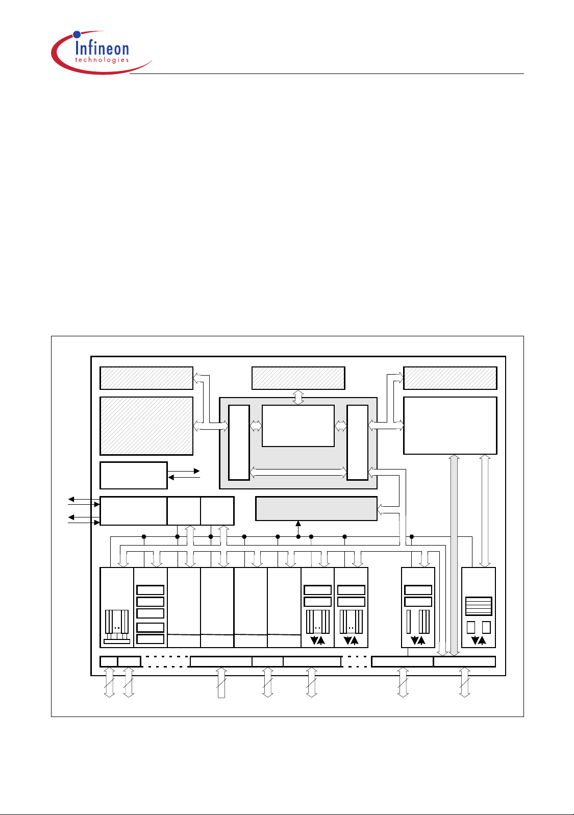
3 Functional Description
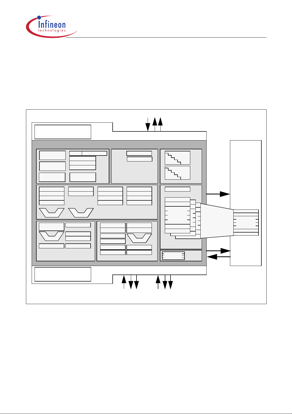
The architecture of the XC164 combines advantages of RISC, CISC, and DSP
processors with an advanced peripheral subsystem in a very well-balanced way. In
addition, the on-chip memory blocks allow the design of compact systems-on-silicon with
maximum performance (computing, control, communication).
The on-chip memory blocks (program code-memory and SRAM, dual-port RAM, data
SRAM) and the set of g eneric perip herals are connected to the CPU via separate bu ses.
Another bus, the LXBus, connects additional on-chip resoures as well as external
resources (see Figure 3).
This bus structure enhances the overall system performance by enabling the concurrent
operation of several subsystems of the XC164.
The following block diagram gives an overview of the different on-chip components and
of the advanced, high bandwidth internal bus structure of the XC164.
PSRAM DPRAM DSRAM
XTAL
ProgMem
Flash / RO M
128 KBytes
OCDS
Debug Support
Osc / PLL
Clock Generation
ADC
8/10-Bit
12/1 6
Channels
P 20
GPT
T2
T3
T4
T5
T6
65
RTC WDT
BRGen
ASC1
(USART)
BRGen
Port 5
ASC0
(USART)
14
PMU
SSC0
(S PI)
BRGen
CPU
C166SV2-Core
Interrupt & PEC
SSC1
(SPI)
BRGen
CC1
T0
T1
148
DMU
Interrupt Bu s
Peripheral Data Bus
CC2
T7
T8
CC6
T12
T13
PORT1 PORT0Port 3Port 4Port 9
16
EBC
XBUS Control
External Bus
Control
Twin
CAN
A B
16
MC B04323_x4.vsd
Figure 3 Block Diagram
Data Sheet 14 V2.1, 2003-06

XC164
Derivatives
Functional Description
3.1 Memory Subsystem and Organization
The memory space of the XC164 is configured in a Von Neumann architecture, which
means that all internal and external resources, such as code memory, data memory,
registers and I/O ports, are organized within the same linear address space. This
common memory space includes 16 Mbytes and is arranged as 256 segments of
64 Kbytes each, where each segment consists of four data pages of 16K bytes each.
The entire memory space can be accessed bytewise or wordwise. Portions of the onchip DPRAM and the register spaces (E/SFR) have additionally been made directly
bitaddressable.
The internal data memory areas and the Special Function Register areas (SFR and
ESFR) are mapped into segment 0, the system segment.
The Program Mana gement Uni t ( PMU) handl es all code fetches and, therefore, contr ols
accesses to the program memories, such as Flash memory, ROM, and PSRAM.
The Data Management Unit (DMU) handles all data transfers and, therefore, controls
accesses to the DSRAM and the on-chip peripherals.
Both units (PMU and DMU) are connected via the high-speed system bus to exchange
data. This is requ ired if operands are re ad from p rogram memory, code or data i s written
to the PSRAM, code is fetched from external memory, or data is read from or written to
external resources, including pe ripherals on the LX bus ( such as TwinCAN). The system
bus allows concurrent two-way communication for maximum transfer performance.
128 Kbytes of on-chip Flash memory or mask-programmable ROM stor e code o r
constant data. The on-chip Flash memory is organized as four 8-Kbyte sectors, one
32-Kbyte sector, and one 64-Kbyte sector. Each sector can be separately write
protected1), erased and programmed (in blocks of 128 Bytes). The complete Flash or
ROM area can be read-protected. A password sequence temporarily unlocks protected
areas. The Flash module combines very fast 64-bit one-cycle read accesses with
protected and efficient writing algorithms for programming and erasing. Thus, program
execution out of the internal Flash results in maximum performance. Dynamic error
correction provides extremely high read data security for all read accesses.
Programming typically takes 2 ms per 128-byte block (5 ms max.), erasing a sector
typically takes 200 ms (500 ms max.).
2 Kbytes of on-chip Program S RAM (PSRAM ) are provided to store user code or data.
The PSRAM is accessed via the PMU and is therefore optimized for code fetches.
2 Kbytes of on-chip Data SRAM (DSRAM ) are provided as a storage for general user
data.The DSRAM is accessed via the DMU and is therefor e optimized for data accesses.
2 Kbytes of on-chip Dual-Port RAM (DPRAM) are provided as a storage for user
defined variables, for the system stack, general purpose register banks. A register bank
can consist of up to 16 wordw ide (R0 to R15) and/or bytew ide (RL0, RH0, …, RL7, RH7)
1)
Each two 8-Kbyte sectors are combined for write-protection purposes.
Data Sheet 15 V2.1, 2003-06
XC164
Derivatives
Functional Description
so-called General Purpose Registers (GPRs).
The upper 256 bytes of the DPRAM are directly bitaddressable. When used by a GPR,
any location in the DPRAM is bitaddressable.
1024 bytes (2 × 512 bytes) of the address space are reserved for the Special Function
Register areas (SFR space and ESFR space). SFRs are wordwide registers which are
used for controlling and monitoring functions of the different on-chip units. Unused SFR
addresses are reserved for future m embers of the XC166 Family. Therefore, they shou ld
either not be accessed, or written with zeros, to ensure upward comp atibility.
In order to meet the needs of designs where more memory is required than is provided
on chip, up to 12 Mbytes (approximately, see Table 3) of exter nal RAM and/or R OM can
be connected to the microcontroll er. Th e External Bus Interfa ce also pr ovides access to
external peripherals.
Table 3 XC164 Memory Map
Address Area Start Loc. End Loc. Area Size
Flash register space FF’F000
Reserved (Acc. trap)
Reserved for PSRAM
F8’0000
E0’0800
Program SRAM E0’0000
Reserved for pr. mem.
C2’0000
Program Flash/ROM C0’0000
Reserved
BF’0000
External memory area 40’0000
External IO area
4)
20’0800
TwinCAN registers 20’0000
External memory area 01’0000
Data RAMs and SFRs 00’8000
External memory area 00’0000
1)
Accesses to the shaded areas generate external bus accesses.
2)
The areas marked with “<“ are slightly smaller than indicated, see column “Notes”.
3)
Not defined register locations return a trap code.
4)
Several pipeline optimizations are not active within the external IO area. This is necessary to control external
peripherals properly.
1)
H
H
H
H
H
H
H
H
H
H
H
H
H
FF’FFFF
FF’EFFF
F7’FFFF
E0’07FF
DF’FFFF
C1’FFFF
BF’FFFF
BE’FFFF
3F’FFFF
20’07FF
1F’FFFF
00’FFFF
00’7FFF
2)
Notes
H
H
H
H
H
H
H
H
H
H
H
H
H
4 Kbytes Flash only
<0.5 Mbytes Minus Flash regs
<1.5 Mbytes Minus PSRAM
2 Kbytes Maximum
< 2 Mbytes Minus Flash/ROM
128 Kbytes
64 Kbytes
<8 Mbytes Minus res. seg.
<2 Mbytes Minus TwinCAN
2 Kbytes
<2 Mbytes Minus segment 0
32 Kbytes Partly used
32 Kbytes
3)
Data Sheet 16 V2.1, 2003-06

XC164
Derivatives
Functional Description
3.2 External Bus Controller
All of the external memory accesses ar e perform ed by a particular on-chi p Ex ternal Bu s
Controller (EBC). It can be programmed either to Single Chip Mode when no external
memory is required, or to one of four different external memory access modes1), which
are as follows:
– 16 … 24-bit Addresses, 16-bit Data, Demultiplexed
– 16 … 24-bit Addresses, 16-bit Data, Multiplexed
– 16 … 24-bit Addresses, 8-bit Data, Multiplexed
– 16 … 24-bit Addresses, 8-bit Data, Demultiplexed
In the demultiplexed bus modes, addresses are output on PORT1 and data is input/
output on PORT0 or P0L, respectively. In the multiplexed bus modes both addresses
and data use PORT0 for input/output. The high order address (segment) lines use
Port 4. The number of active segment address lines is selectable, re stricting the extern al
address space to 8 Mbytes … 64 Kbytes. This is required when interface lines are
assigned to Port 4.
Up to 4 external CS signals (3 windows plus default) can be generated in order to save
external glue logic. E xternal modules can di rectly be connecte d to the common address/
data bus and their individual select lines.
Important timing characteristics of the external bus interface have been made
programmable (via registers TCONCSx/FCONCSx) to allow the user the adaption of a
wide range of different types of memories and external peripherals.
In addition, up to 4 independent address windows may be defined (via registers
ADDRSELx) which control the access to different resources with different bus
characteristics. These address windows are arranged hierarchically where window 4
overrides window 3, and window 2 overrides window 1. All accesses to locations not
covered by these 4 address windows are controlled by TCONCS0/FCONCS0. The
currently active window can generate a chip select signal.
The external bus timing is related to the rising edge of the reference clock output
CLKOUT. The external bus protocol is compatible w ith that of the standard C166 Family.
The EBC also controls accesses to resources connected to the on-chip LXBus. The
LXBus is an internal representation of the external bus and allows accessing integrated
peripherals and modules in the same way as external components.
The TwinCAN module is connected and accessed via the LXBus.
1)
Bus modes are switched dynamically if several address windows with different mode settings are used.
Data Sheet 17 V2.1, 2003-06
XC164
Derivatives
Functional Description
3.3 Central Processing Unit (CPU)
The main core of the CPU consists of a 5-stage execution pipeline with a 2-stage
instruction-fetch pipeline, a 1 6-bit arithme tic an d logic u nit (ALU), a 32-bi t/40-bi t multi ply
and accumulate unit (MA C), a register- fi le providi ng th ree r egister banks, and dedicated
SFRs. The ALU features a multiply and divide unit, a bit-mask generator, and a barrel
shifter.
System-Bus
Internal Program M em o ry
CPU
Prefetch Unit
Branch Unit
FIFO
IDX0
IDX1
QX0
QX1
Multiply Unit
+/-
MAH
CSP
CPUCON 1
CPUCON2
CPUID
Return Stack
QR0
QR1
+/-+/-
MRW
MCW
MSW
MAL
MAC
PMU
IP
IFU
Injection/Exception
DPP0
DPP1
DPP2
DPP3
Division Unit
Multiply Unit
MDC
PSW
Zeros
data in
VECSEG
TFR
Handler
SPSEG
SP
STKOV
STKUN
ADU
Bit-Mask-Gen.
Barrel-Shifter
+/-
MDLMDH
Ones
ALU
address
data out
data in
address
da ta ou t
DPRAM
2-Stage
Prefetch
Pipeline
5-Stage
Pipeline
IPIP
CP
R15
R14
GPRs
R1
R0
R15
R14
GPRs
GPRs
R1
R0
R15
R14
R1
R0
address
R15
R14
GPRs
R1
R0
RF
data in
Buffer
address
data out
data in
WB
data out
SRAM
DMU
Peripheral-Bus
System-Bus
Figure 4 CPU Block Diagram
Based on these hardware provisions, mo st of the XC164’s instructions can be executed
in just one machine cycle which requir es 25 ns at 40 MHz CPU clock. For example, shift
and rotate instructions are always processed during one machine cycle independent of
the number of bits to be shifted. Also multiplication and most MAC instructions execute
in one single cycle. All multi ple -cycl e instructions have been optimized so that they can
be executed very fast as well: for e xample, a 32-/16-bit division is started within 4 cycles,
while the remaining 15 cycles are executed in the background. Another pipeline
Data Sheet 18 V2.1, 2003-06
 Loading...