

Page 1
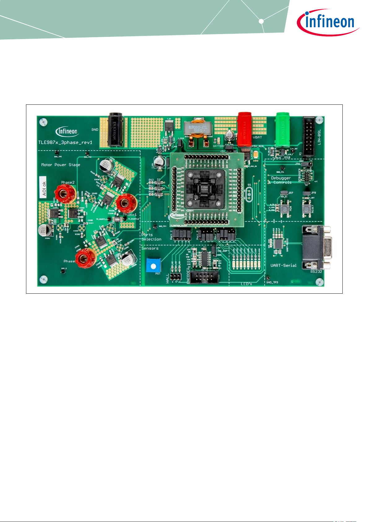
TLE987x EvalBoard Rev1.2 User Manual
About this document
Scope and purpose
This user manual is intented to help users using the TLE987x Evalboard. This Evalboard is designed to evaluate
hardware and software functionalities of the TLE987x device family.
This manual provides additional information about the board’s layout, jumper settings, interface and debug
options. It introduces the evaluation platform as well as how to write software and download it to the TLE987x.
Intended audience
This document is for everyone who works with the TLE987x Evalboard.
User Manual Please read the Important Notice and Warnings at the end of this document Rev. 1.0
www.infineon.com page 1 of 20 2019-04-15
Page 2

TLE987x EvalBoard User Manual
About this document
Abbreviation
Definition
BLDC
Brushless direct current
BSL
Bootstrap loader
GH1, 2, 3
Gate high-side MOSFETs for phases 1, 2
GL1, 2, 3
Gate low-side MOSFETs for phase 1, 2
GPIO
General purpose input / output
ISP
In-system programmer
LIN
Local interconnect network
MON
Monitor
n.c.
Not connected
n/u
Not used
OP1
Negative operational amplifier input
OP2
Positive operational amplifier input
RST
Reset
SL
Source low-side MOSFET
SWD
Arm® serial wire debug
TMS
Test mode select
UART
Universal asynchronous receiver transmitter
VAREF
Reference voltage
VBAT
Battery voltage supply
VCOM
Virtual COM-port
VCP
Voltage charge pump
VDDC
Core supply
VDDEXT
External voltage supply output
VDDP
I/O port supply
VDH
Voltage drain high-side MOSFET
VS
Battery supply input
VSD
Battery supply input for MOSFET driver
Abbreviations and definitions
Table 1 Abbreviations
User Manual 2 of 20 Rev. 1.0
2019-04-15
Page 3

TLE987x EvalBoard User Manual
Table of contents
Table of contents
About this document ....................................................................................................................... 1
Table of contents ............................................................................................................................ 3
1 Concept ................................................................................................................................ 4
2 Interconnects ........................................................................................................................ 5
3 Test points and LEDs ............................................................................................................... 7
4 Jumper settings ..................................................................................................................... 8
5 Communication interfaces ..................................................................................................... 10
5.1 LIN (via banana jack and uIO BSL) ........................................................................................................ 10
5.2 UART ...................................................................................................................................................... 10
5.3 Debugging .............................................................................................................................................. 10
6 Software toolchain ................................................................................................................ 11
6.1 Keil µVision 5 ......................................................................................................................................... 11
6.2 Infineon ConfigWizard ........................................................................................................................... 11
6.3 TLE987x SDK .......................................................................................................................................... 11
6.4 Debug connection setup ....................................................................................................................... 11
7 Technical data ...................................................................................................................... 13
8 Optional additional placements .............................................................................................. 14
9 Schematics and layout ........................................................................................................... 16
9.1 Schematic .............................................................................................................................................. 16
9.2 Layout .................................................................................................................................................... 19
User Manual 3 of 20 Rev. 1.0
2019-04-15
Page 4
TLE987x EvalBoard User Manual
Concept
1 Concept
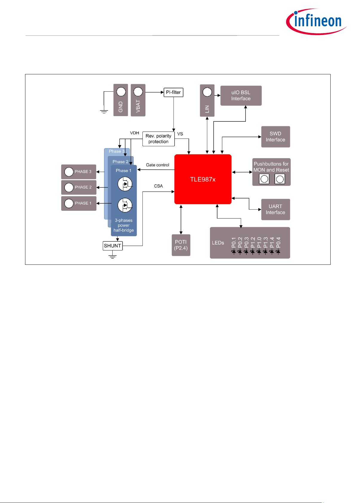
Figure 1 Board concept
This board is designed to provide a simple, easy-to-use tool for getting familiar with Infineon’s Embedded
Power IC TLE987x devices. A socket provides the possibility to test and evaluate all ICs of the TLE987x family.
Every pin of the IC is connectable via rows of pin headers. The board is protected against reverse polarity of
input voltage supply.
Three MOSFET half bridges are assembled on the board to drive a BLDC motor. The board is ready to be
connected to a car supply or similar and offers a SWD port to connect an external debugger.
The evaluation board can be operated by standard laboratory equipment as power supply and LIN
communication are working via banana jacks.
There is a battery LED that indicates that the board is connected to supply in the correct way. Otherwise
reverse polarity protection secures the board from damage by cross connection.
User Manual 4 of 20 Rev. 1.0
2019-04-15
Page 5
TLE987x EvalBoard User Manual
Interconnects
GND
Phase 2
Phase 1
SWD
UART-
Serial
VBAT
LIN
uIO-
Stick
Phase 3
VBAT
uIO tick
2 Interconnects
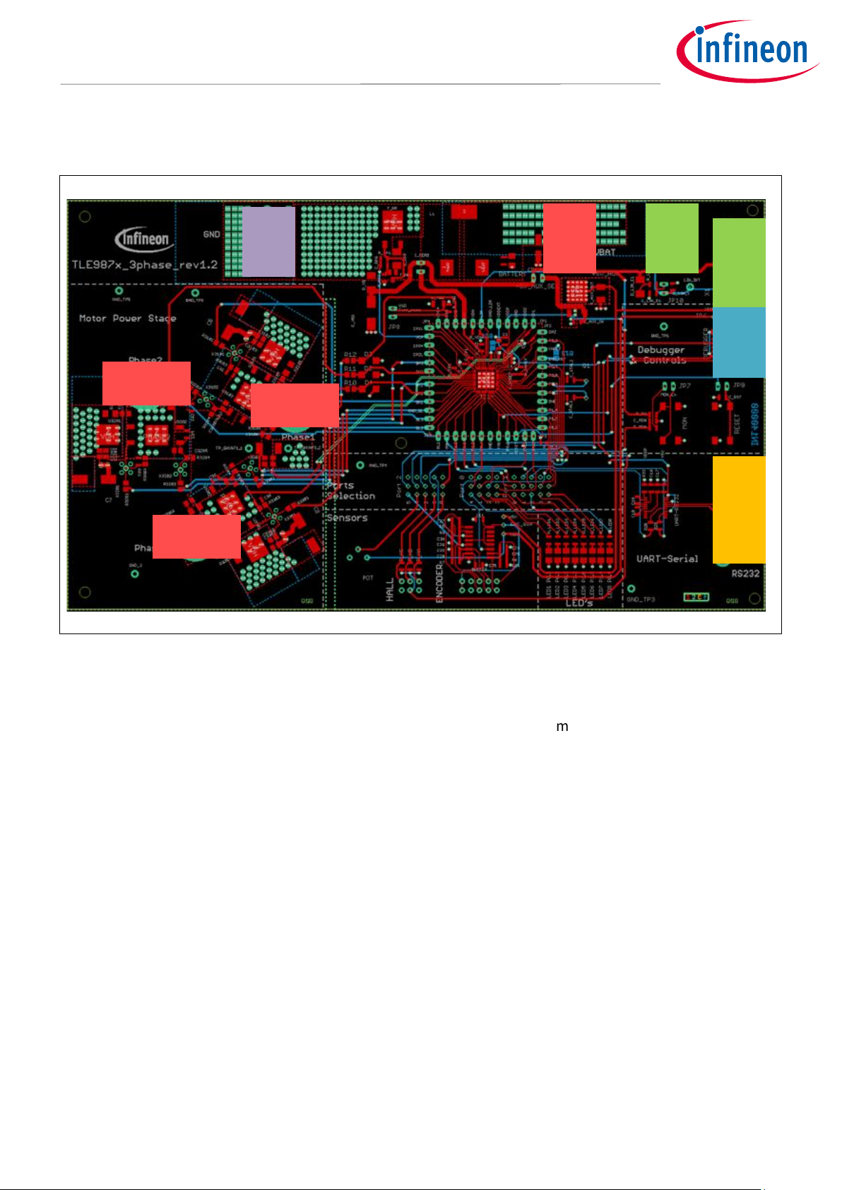
Figure 2 Interconnects
Banana jacks for ground, supply and LIN
There are jacks in different colors for ground, supply (max. 28 V) and LIN communication via banana jack. The
following jacks are available: GND (marked purple), VBAT (marked red) and LIN (marked green).
Terminal pins for motor connection (marked red)
The three pins Phase1, Phase 2 and Phase3 provide access to the three half bridges and are intended to
connect a brushless motor.
uIO Stick connector (marked green)
This uIO bootstrap loader is a 16-pin header (2 x 8) with 2.54 mm pitch.
It is intended to connect additional hardware for bootstrap loading. This interface can be used to programming
the TLE987x via LIN (see www.infineon.com/uio or www.hitex.com/uio).
User Manual 5 of 20 Rev. 1.0
2019-04-15
Page 6
TLE987x EvalBoard User Manual
Interconnects
5 V 1 2
3 4
5 6
7 8
GND
GND
n.c.
SWDIO (TMS)
SWCLK (P0.0)
n.c.
n.c.
9 10DBPRE RESET
LIN RESET
GND
VS_PRE
n.c.
n.c.
n.c.
n.c.
1 2 3 4 5 6 7
8
9
11
10
13
14
15
16
n.c. n.c. n.c.
n.c.
n.c.
n.c.
n.c.
n.c.
12
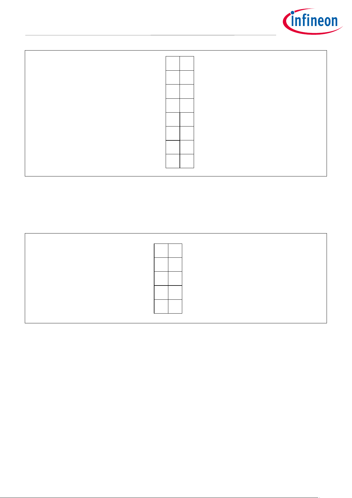
Figure 3 Pin configuration uIO BSL
Pin header for SWD (marked blue)
There is a 10 pin header (2 x 5) with 1.27 mm pitch on the evaluation board. This interface is meant to be used
for debugging.
Figure 4 Pin configuration SWD interface
User Manual 6 of 20 Rev. 1.0
2019-04-15
Page 7

TLE987x EvalBoard User Manual
Test points and LEDs
GND
Shunt 1.2
Vbat LED
GND
GND
LEDs 1-8
GND
Shunt 1.1
GND
LIN INT
GND
3 Test points and LEDs
Figure 5 Test points
Several ground test points are provided.
Test points Shunt 1.1 and Shunt 1.2 are provided at both sides of the shunt, which is 5 mR.
Test point LIN_INT is used to measure the LIN voltage.
There are 9 LEDs for visual validations on the board:
LED 1 to 8 can be connected to GPIOs (see Table 3).
LED 9 (Vbat LED) indicates power supply.
User Manual 7 of 20 Rev. 1.0
2019-04-15
Page 8

TLE987x EvalBoard User Manual
Jumper settings
JP7
Close this jumper to connect MON button to MON input. Open it to disconnect MON
button from MON input.
JP8
This jumper is closed by default. If this jumper is left open the device is not supplied. It is
intended to open the VS line in order to measure the current flowing into the TLE987x
device.
JP9
Close this jumper to connect RESET button to RESET input. Open it to disconnect RESET
button from RESET input.
JP10
Close this jumper to connect an additional 1 kΩ pull-up resistor. This is intended for LIN
master communication. Open the jumper to use the TLE987x as slave in a LIN network.
Software for LIN low level driver can be found at the homepage of IHR (www.ihr.de).
I_MEAS
This jumper is closed by default. If this jumper is left open the device is not supplied. It is
intended to open the VSD line in order to measure the current flowing into the TLE987x
device.
+5V_AUX_SEL
Open this jumper to disable the board’s voltage regulator.
PORT 0/1/2
These jumpers can be put in two different positions (see Figure 7). Change these jumpers
positon to connect or disconnect the LEDs, the potentiometer, the encoder or the Hall
sensor (see Table 3).
+5V_AUX_SEL
JP8
Port 2
Port 0
Port 1
I_MEAS
JP10
JP7
JP9
4 Jumper settings
Figure 6 Jumpers
Table 2 Jumpers
User Manual 8 of 20 Rev. 1.0
2019-04-15
Page 9

TLE987x EvalBoard User Manual
Jumper settings
Port
Position 1
Position 2
P0.1
LED 1
Encoder
P0.2
LED 2
/
P0.3
LED 3
/
P0.4
LED 8
/
P1.0
LED 5
/
P1.1
/
UART
P1.2
LED 4
UART
P1.3
LED 6
/
P1.4
LED 7
/
P2.0
Hall A
/
P2.4
POTI
/
P2.2
Hall C
/
P2.3
Hall B
Encoder
P2.5
Encoder
/
Jumper in position 2
Jumper in position 1
Figure 7 Jumper position
Table 3 GPIOs’ function
User Manual 9 of 20 Rev. 1.0
2019-04-15
Page 10

TLE987x EvalBoard User Manual
Communication interfaces
5 Communication interfaces
5.1 LIN (via banana jack and uIO BSL)
The device integrated LIN transceiver is connected to a banana jack and additionally to the uIO BSL interface.
To integrate the device in a LIN network it is sufficient to use the single wire banana interface. The BSL interface
is intended to program the device via LIN. For further information about the uIO interface see
www.infineon.com/uio or www.hitex.com/uio.
5.2 UART
A RS232 connector on the board enables a serial communication.
5.3 Debugging
Debugging is possible via the SWD interface; the signals are routed through the 10 pin header SWD interface
The pin configuration makes sure that the XMC is hold in reset while another debugger is physically connected
as DBPRE will be implicitly connected to GND by connecting the external ISP (see Figure 4).
User Manual 10 of 20 Rev. 1.0
2019-04-15
Page 11

TLE987x EvalBoard User Manual
Software toolchain
6 Software toolchain
6.1 Keil µVision 5
The recommended Integrated Software Development Environment is Keil® µVision5®.
Infineon’s Embedded Power family is supported. For more information about the installation process, go to
www.keil.com.
6.2 Infineon ConfigWizard
In addition to the IDE, Infineon provides a solution to speed-up the IC programming, the “ConfigWizard”. This
tool is designed for code configuration in combination with the IDE. Infineon ConfigWizard can be downloaded
via the Infineon Toolbox. The Infineon Toolbox is a central place to download and update all your Infineon
tools. It can be downloaded from www.infineon.com/toolbox.
6.3 TLE987x SDK
All Embedded Power products can be installed to Keil® µVision5® via “Pack Installer”. Browsing to the Infineon
chapter in “All Devices” will lead to the “TLE98xx Series”. The “.pack” file comes with several code examples to
provide an easy start up and speed up software development.
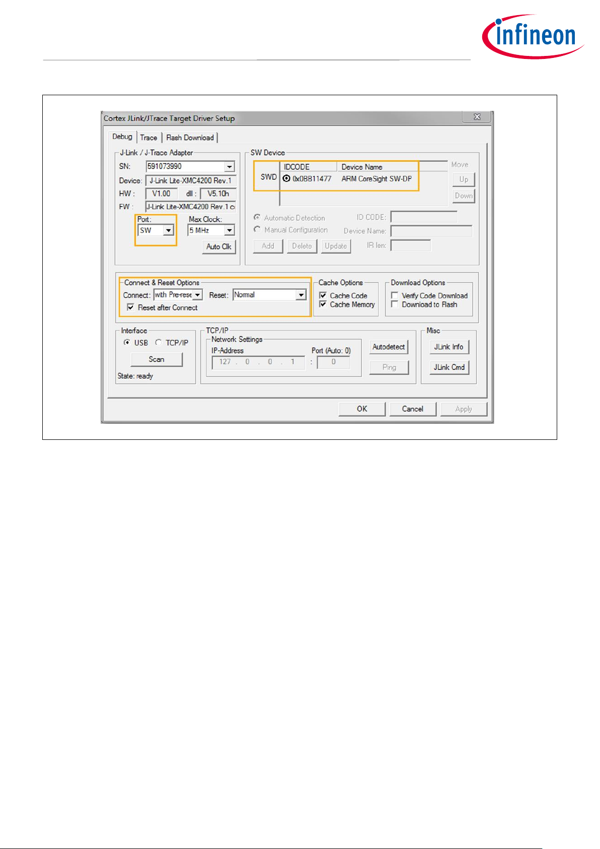
6.4 Debug connection setup
For a proper Flash and Debug Connection, install V5.10 (or newer) from: www.segger.com/jlink-
software.html. Keil® µVision5® has to be configured in the IDE Menu “Options for Target”. After connecting the
USB-cable and power up the EvalBoard, go to the “Debug” register-card, choose “J-LINK / J-TRACE Cortex” and
press “Settings”.
User Manual 11 of 20 Rev. 1.0
2019-04-15
Page 12
TLE987x EvalBoard User Manual
Software toolchain
Figure 8 Debug and flash configuration
If the board is connected successfully, the Arm® IDCODE will be visible in the SW Device Window. If connection
fails, “Connect & Reset Options” and “Port” window has to be checked.
User Manual 12 of 20 Rev. 1.0
2019-04-15
Page 13

TLE987x EvalBoard User Manual
Technical data
Voltage supply:
max. 28 V
Motor current:
max. 20 A
Pin ports:
5 V
7 Technical data
Table 4 Technical data
User Manual 13 of 20 Rev. 1.0
2019-04-15
Page 14
TLE987x EvalBoard User Manual
Optional additional placements
Component
Description
Q1
External oscillator
C_XTAL1
Oscillator capacitor 1
C_XTAL2
Oscillator capacitor 2
R3105
Resistance snubber high-side MOSFET phase 1
C3104
Capacitor snubber high-side MOSFET phase 1
C3103
Gate drain capacitor high-side MOSFET phase 1
R3106
Resistance snubber low-side MOSFET phase 1
C3106
Capacitor snubber low-side MOSFET phase 1
C3105
Gate drain capacitor low-side MOSFET phase 1
R3205
Resistance snubber high-side MOSFET phase 2
C3204
Capacitor snubber high-side MOSFET phase 2
C3203
Gate drain capacitor high-side MOSFET phase 2
R3206
Resistance snubber low-side MOSFET phase 2
R3205
C3205
C3204
R3206
C3206
C3203
C3306
R3306
C3304
R3305
R3303
R3304
C3105
C3106
R3106
C3103
C3104
R3105
Q1
C_XTAL2C_XTAL1
8 Optional additional placements
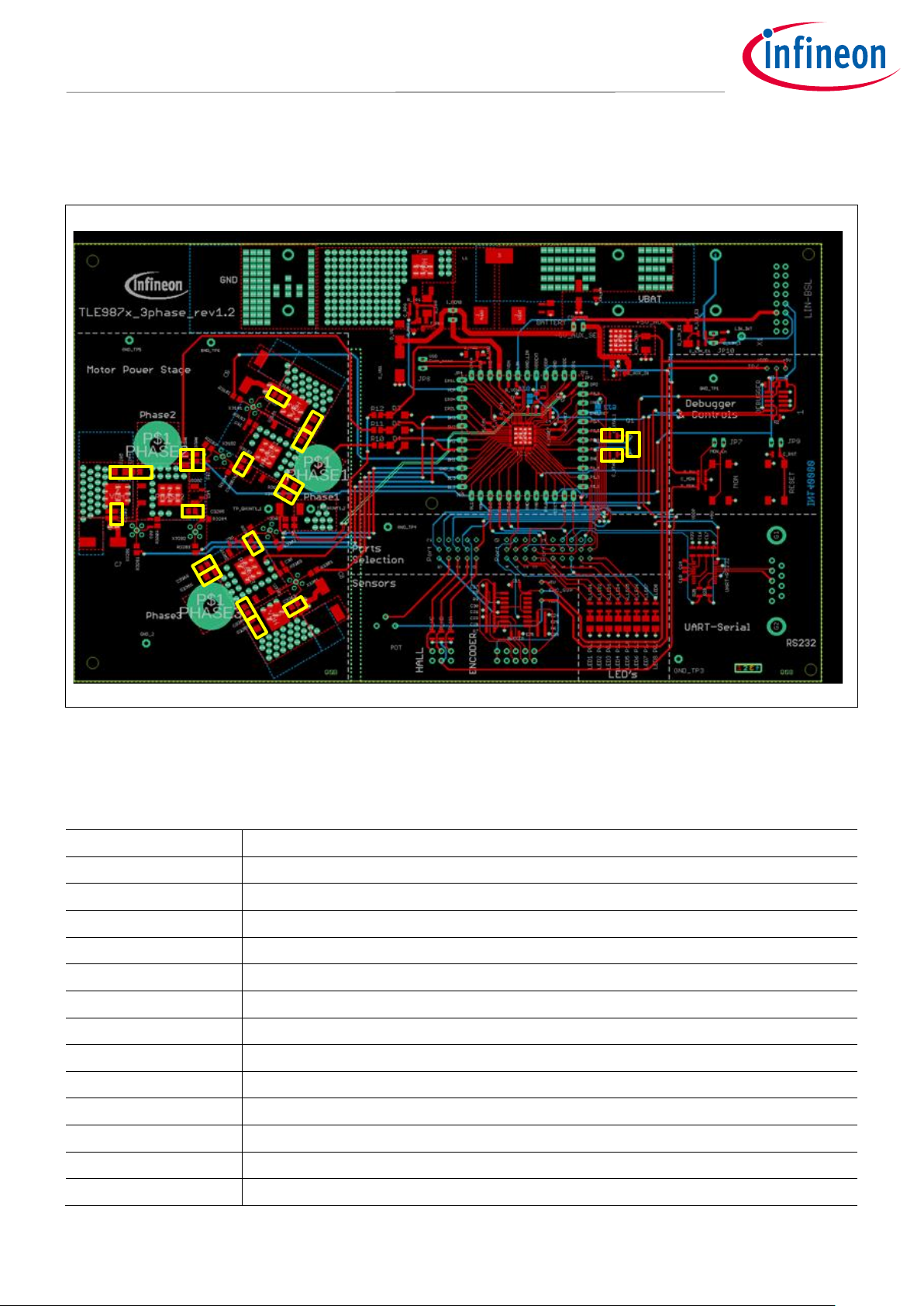
Figure 9 Additional placements’ positions
Values for these optional additional placements have to be determined depending on application.
Table 5 Additional placements
User Manual 14 of 20 Rev. 1.0
2019-04-15
Page 15

TLE987x EvalBoard User Manual
Optional additional placements
Component
Description
C3206
Capacitor snubber low-side MOSFET phase 2
C3205
Gate drain capacitor low-side MOSFET phase2
R3305
Resistance snubber high-side MOSFET phase 3
C3304
Capacitor snubber high-side MOSFET phase 3
C3303
Gate drain capacitor high-side MOSFET phase 3
R3306
Resistance snubber low-side MOSFET phase 3
C3306
Capacitor snubber low-side MOSFET phase 3
C3305
Gate drain capacitor low-side MOSFET phase 3
User Manual 15 of 20 Rev. 1.0
2019-04-15
Page 16
TLE987x EvalBoard User Manual
Schematics and layout
9 Schematics and layout
9.1 Schematic
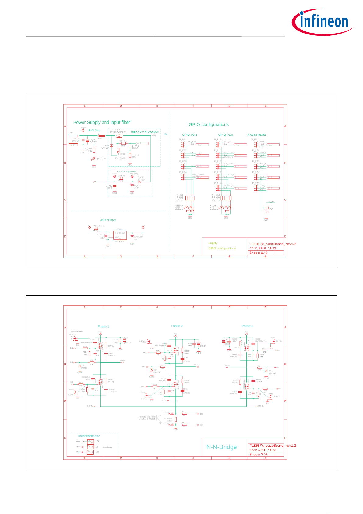
Figure 10 Schematics: Sheet 1
Figure 11 Schematics: Sheet 2
User Manual 16 of 20 Rev. 1.0
2019-04-15
Page 17
TLE987x EvalBoard User Manual
Schematics and layout
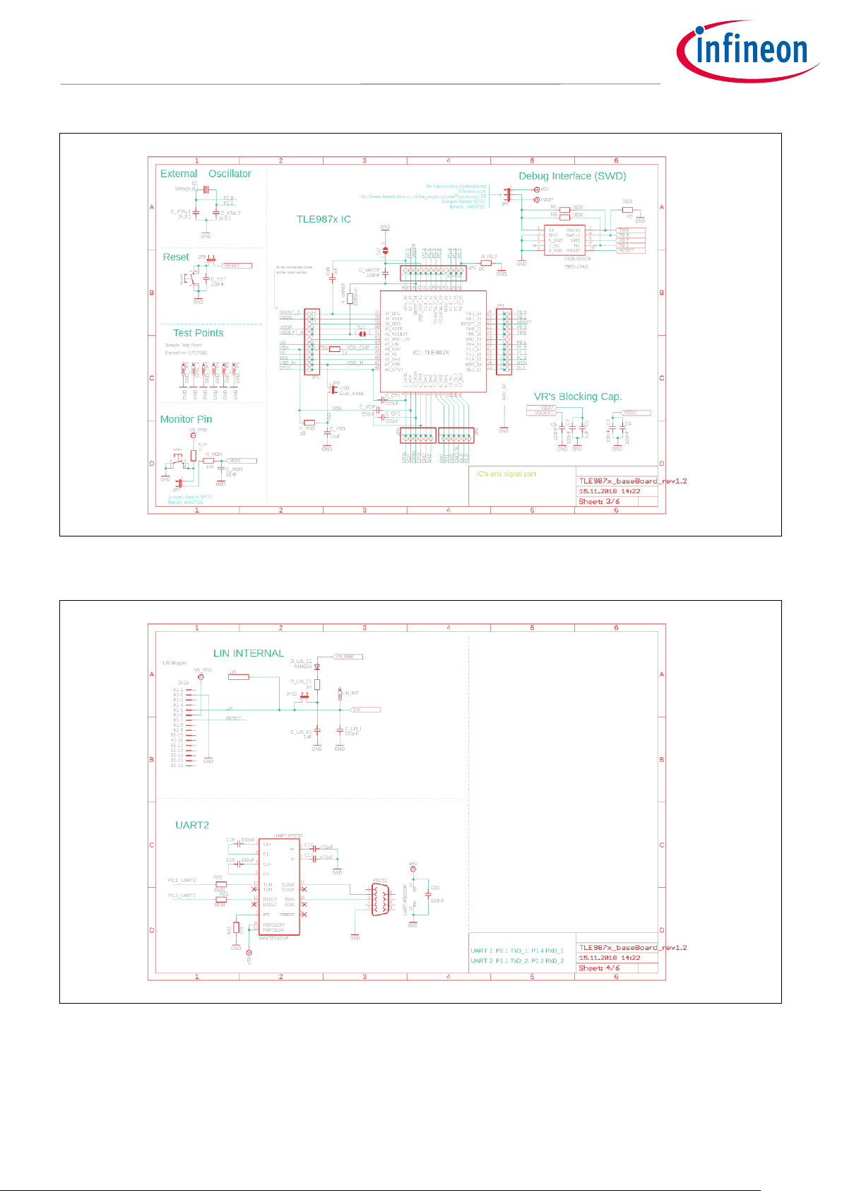
Figure 12 Schematics: Sheet 3
Figure 13 Schematics: Sheet 4
User Manual 17 of 20 Rev. 1.0
2019-04-15
Page 18
TLE987x EvalBoard User Manual
Schematics and layout
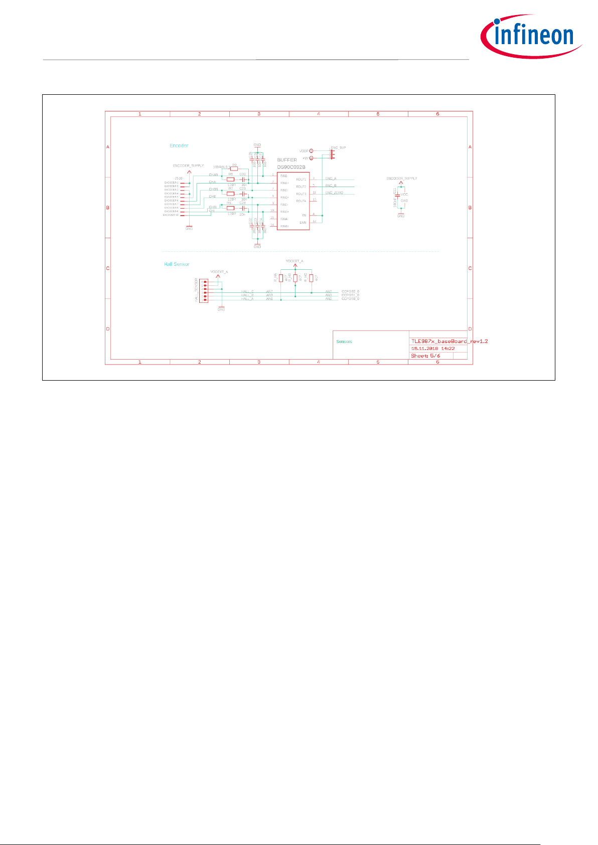
Figure 14 Schematics: Sheet 5
User Manual 18 of 20 Rev. 1.0
2019-04-15
Page 19
TLE987x EvalBoard User Manual
Schematics and layout
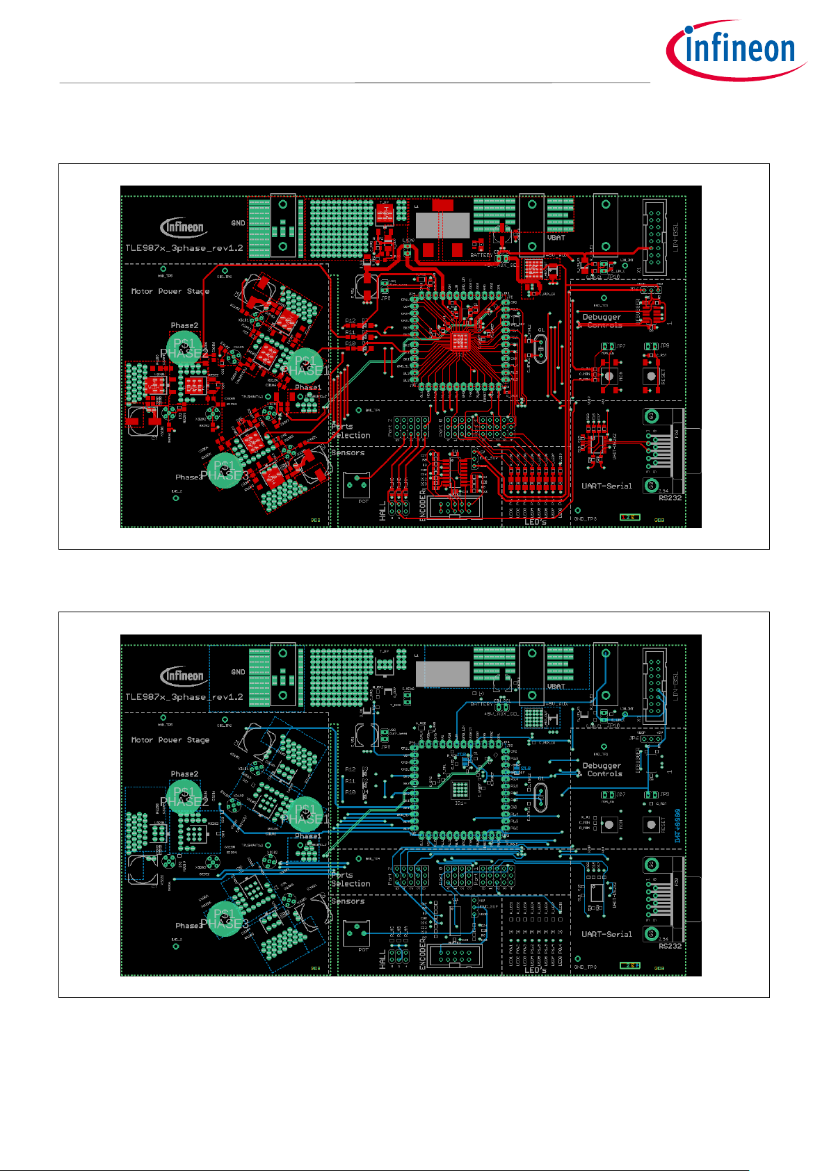
9.2 Layout
Figure 15 Top layer
Figure 16 Bottom layer
User Manual 19 of 20 Rev. 1.0
2019-04-15
Page 20

Trademarks
All referenced product or service names and trademarks are the property of their respective owners.
Edition 2019-04-12
Published by
Infineon Technologies AG
81726 Munich, Germany
© 2019 Infineon Technologies AG.
All Rights Reserved.
Do you have a question about this
document?
Email: [email protected]
Document reference
IMPORTANT NOTICE
The information given in this document shall in no
event be regarded as a guarantee of conditions or
characteristics (“Beschaffenheitsgarantie”).
With respect to any examples, hints or any typical
values stated herein and/or any information
regarding the application of the product, Infineon
Technologies hereby disclaims any and all
warranties and liabilities of any kind, including
without limitation warranties of non-infringement
of intellectual property rights of any third party.
In addition, any information given in this document
is subject to customer’s compliance with its
obligations stated in this document and any
applicable legal requirements, norms and
standards concerning customer’s products and any
use of the product of Infineon Technologies in
customer’s applications.
The data contained in this document is exclusively
intended for technically trained staff. It is the
responsibility of customer’s technical departments
to evaluate the suitability of the product for the
intended application and the completeness of the
product information given in this document with
respect to such application.
For further information on the product, technology,
delivery terms and conditions and prices please
contact your nearest Infineon Technologies office
(www.infineon.com).
WARNINGS
Due to technical requirements products may
contain dangerous substances. For information on
the types in question please contact your nearest
Infineon Technologies office.
Except as otherwise explicitly approved by Infineon
Technologies in a written document signed by
authorized representatives of Infineon
Technologies, Infineon Technologies’ products may
not be used in any applications where a failure of
the product or any consequences of the use thereof
can reasonably be expected to result in personal
injury.
 Loading...