


Angle Sensor
GMR-Based Angle Sensor
TLE5012B
User’s Manual
Rev. 1.2, 2018-02
User’s Manual
Sense & Control

Edition 2018-02
Published by
Infineon Technologies AG
81726 Munich, Germany
© 2018 Infineon Technologies AG
All Rights Reserved.
Legal Disclaimer
The information given in this document shall in no event be regarded as a guarantee of conditions or
characteristics. With respect to any examples or hints given herein, any typical values stated herein and/or any
information regarding the application of the device, Infineon Technologies hereby disclaims any and all warranties
and liabilities of any kind, including without limitation, warranties of non-infringement of intellectual property rights
of any third party.
Information
For further information on technology, delivery terms and conditions and prices, please contact the nearest
Infineon Technologies Office (www.infineon.com).
Warnings
Due to technical requirements, components may contain dangerous substances. For information on the types in
question, please contact the nearest Infineon Technologies Office.
Infineon Technologies components may be used in life-support devices or systems only with the express written
approval of Infineon Technologies, if a failure of such components can reasonably be expected to cause the failure
of that life-support device or system or to affect the safety or effectiveness of that device or system. Life support
devices or systems are intended to be implanted in the human body or to support and/or maintain and sustain
and/or protect human life. If they fail, it is reasonable to assume that the health of the user or other persons may
be endangered.

TLE5012B
Revision History
Page or Item Subjects (major changes since previous revision)
Rev. 1.2, 2018-02
Chapter 5.2.4 Update STAT and RESP in CRC calculation
Chapter 6.1.4 Add explanation when ANG_DIR = 1
Figure 6-1 Update STAT register
Chapter 3 Uptade Chapter 3
Chapter 5.6 Add footnote regarding maximum rotation speed
Chapter 6.2.1 Update S_MAGOL definition
Trademarks of Infineon Technologies AG
AURIX™, C166™, CanPAK™, CIPOS™, CIPURSE™, EconoPACK™, CoolMOS™, CoolSET™,
CORECONTROL™, CROSSAVE™, DAVE™, DI-POL™, EasyPIM™, EconoBRIDGE™, EconoDUAL™,
EconoPIM™, EconoPACK™, EiceDRIVER™, eupec™, FCOS™, HITFET™, HybridPACK™, I²RF™,
ISOFACE™, IsoPACK™, MIPAQ™, ModSTACK™, my-d™, NovalithIC™, OptiMOS™, ORIGA™,
POWERCODE™; PRIMARION™, PrimePACK™, PrimeSTACK™, PRO-SIL™, PROFET™, RASIC™,
ReverSave™, SatRIC™, SIEGET™, SINDRION™, SIPMOS™, SmartLEWIS™, SOLID FLASH™, TEMPFET™,
thinQ!™, TRENCHSTOP™, TriCore™.
Other Trademarks
Advance Design System™ (ADS) of Agilent Technologies, AMBA™, ARM™, MULTI-ICE™, KEIL™,
PRIMECELL™, REALVIEW™, THUMB™, µVision™ of ARM Limited, UK. AUTOSAR™ is licensed by AUTOSAR
development partnership. Bluetooth™ of Bluetooth SIG Inc. CAT-iq™ of DECT Forum. COLOSSUS™,
FirstGPS™ of Trimble Navigation Ltd. EMV™ of EMVCo, LLC (Visa Holdings Inc.). EPCOS™ of Epcos AG.
FLEXGO™ of Microsoft Corporation. FlexRay™ is licensed by FlexRay Consortium. HYPERTERMINAL™ of
Hilgraeve Incorporated. IEC™ of Commission Electrotechnique Internationale. IrDA™ of Infrared Data
Association Corporation. ISO™ of INTERNATIONAL ORGANIZATION FOR STANDARDIZATION. MATLAB™ of
MathWorks, Inc. MAXIM™ of Maxim Integrated Products, Inc. MICROTEC™, NUCLEUS™ of Mentor Graphics
Corporation. MIPI™ of MIPI Alliance, Inc. MIPS™ of MIPS Technologies, Inc., USA. muRata™ of MURATA
MANUFACTURING CO., MICROWAVE OFFICE™ (MWO) of Applied Wave Research Inc., OmniVision™ of
OmniVision Technologies, Inc. Openwave™ Openwave Systems Inc. RED HAT™ Red Hat, Inc. RFMD™ RF
Micro Devices, Inc. SIRIUS™ of Sirius Satellite Radio Inc. SOLARIS™ of Sun Microsystems, Inc. SPANSION™
of Spansion LLC Ltd. Symbian™ of Symbian Software Limited. TAIYO YUDEN™ of Taiyo Yuden Co.
TEAKLITE™ of CEVA, Inc. TEKTRONIX™ of Tektronix Inc. TOKO™ of TOKO KABUSHIKI KAISHA TA. UNIX™
of X/Open Company Limited. VERILOG™, PALLADIUM™ of Cadence Design Systems, Inc. VLYNQ™ of Texas
Instruments Incorporated. VXWORKS™, WIND RIVER™ of WIND RIVER SYSTEMS, INC. ZETEX™ of Diodes
Zetex Limited.
Last Trademarks Update 2011-11-11
User’s Manual 3 Rev. 1.2, 2018-02

TLE5012B
Table of Contents
Table of Contents
Table of Contents . . . . . . . . . . . . . . . . . . . . . . . . . . . . . . . . . . . . . . . . . . . . . . . . . . . . . . . . . . . . . . . . 4
List of Figures . . . . . . . . . . . . . . . . . . . . . . . . . . . . . . . . . . . . . . . . . . . . . . . . . . . . . . . . . . . . . . . . . . . 6
List of Tables . . . . . . . . . . . . . . . . . . . . . . . . . . . . . . . . . . . . . . . . . . . . . . . . . . . . . . . . . . . . . . . . . . . . 8
1 Product Description . . . . . . . . . . . . . . . . . . . . . . . . . . . . . . . . . . . . . . . . . . . . . . . . . . . . . . . . . . . . . . 9
1.1 Overview . . . . . . . . . . . . . . . . . . . . . . . . . . . . . . . . . . . . . . . . . . . . . . . . . . . . . . . . . . . . . . . . . . . . . . . . 9
1.2 Features . . . . . . . . . . . . . . . . . . . . . . . . . . . . . . . . . . . . . . . . . . . . . . . . . . . . . . . . . . . . . . . . . . . . . . . 10
1.3 Application Example . . . . . . . . . . . . . . . . . . . . . . . . . . . . . . . . . . . . . . . . . . . . . . . . . . . . . . . . . . . . . . 10
2 Functional Description . . . . . . . . . . . . . . . . . . . . . . . . . . . . . . . . . . . . . . . . . . . . . . . . . . . . . . . . . . . 11
2.1 Block Diagram . . . . . . . . . . . . . . . . . . . . . . . . . . . . . . . . . . . . . . . . . . . . . . . . . . . . . . . . . . . . . . . . . . 11
2.2 Functional Block Description . . . . . . . . . . . . . . . . . . . . . . . . . . . . . . . . . . . . . . . . . . . . . . . . . . . . . . . 11
2.2.1 Internal Power Supply . . . . . . . . . . . . . . . . . . . . . . . . . . . . . . . . . . . . . . . . . . . . . . . . . . . . . . . . . . . 11
2.2.2 Oscillator and PLL . . . . . . . . . . . . . . . . . . . . . . . . . . . . . . . . . . . . . . . . . . . . . . . . . . . . . . . . . . . . . . 11
2.2.3 SD-ADC . . . . . . . . . . . . . . . . . . . . . . . . . . . . . . . . . . . . . . . . . . . . . . . . . . . . . . . . . . . . . . . . . . . . . . 12
2.2.4 Digital Signal Processing Unit . . . . . . . . . . . . . . . . . . . . . . . . . . . . . . . . . . . . . . . . . . . . . . . . . . . . . 12
2.2.5 Interfaces . . . . . . . . . . . . . . . . . . . . . . . . . . . . . . . . . . . . . . . . . . . . . . . . . . . . . . . . . . . . . . . . . . . . . 13
2.2.6 Safety Features . . . . . . . . . . . . . . . . . . . . . . . . . . . . . . . . . . . . . . . . . . . . . . . . . . . . . . . . . . . . . . . . 13
2.3 Sensing Principle . . . . . . . . . . . . . . . . . . . . . . . . . . . . . . . . . . . . . . . . . . . . . . . . . . . . . . . . . . . . . . . . 14
2.4 Pin Configuration . . . . . . . . . . . . . . . . . . . . . . . . . . . . . . . . . . . . . . . . . . . . . . . . . . . . . . . . . . . . . . . . 16
2.5 Pin Description . . . . . . . . . . . . . . . . . . . . . . . . . . . . . . . . . . . . . . . . . . . . . . . . . . . . . . . . . . . . . . . . . . 16
3 Application Circuits . . . . . . . . . . . . . . . . . . . . . . . . . . . . . . . . . . . . . . . . . . . . . . . . . . . . . . . . . . . . . 17
3.1 IIF interface and SSC (IIF in push-pull configuration) . . . . . . . . . . . . . . . . . . . . . . . . . . . . . . . . . . . . . 17
3.2 HSM interface and SSC (HSM in push-pull configuration) . . . . . . . . . . . . . . . . . . . . . . . . . . . . . . . . . 17
3.3 HSM interface and SSC (HSM in open-drain configuration) . . . . . . . . . . . . . . . . . . . . . . . . . . . . . . . . 18
3.4 PWM interface (push-pull configuration) . . . . . . . . . . . . . . . . . . . . . . . . . . . . . . . . . . . . . . . . . . . . . . . 18
3.5 PWM interface (open-drain configuration) . . . . . . . . . . . . . . . . . . . . . . . . . . . . . . . . . . . . . . . . . . . . . 19
3.6 SPC interface . . . . . . . . . . . . . . . . . . . . . . . . . . . . . . . . . . . . . . . . . . . . . . . . . . . . . . . . . . . . . . . . . . . 19
3.7 SSC interface (push-pull configuration) . . . . . . . . . . . . . . . . . . . . . . . . . . . . . . . . . . . . . . . . . . . . . . . 20
3.8 SSC interface (open-drain configuration) . . . . . . . . . . . . . . . . . . . . . . . . . . . . . . . . . . . . . . . . . . . . . . 20
3.9 Sensor supply in bus mode . . . . . . . . . . . . . . . . . . . . . . . . . . . . . . . . . . . . . . . . . . . . . . . . . . . . . . . . 21
4 Specification . . . . . . . . . . . . . . . . . . . . . . . . . . . . . . . . . . . . . . . . . . . . . . . . . . . . . . . . . . . . . . . . . . . 22
4.1 Autocalibration . . . . . . . . . . . . . . . . . . . . . . . . . . . . . . . . . . . . . . . . . . . . . . . . . . . . . . . . . . . . . . . . . . 22
4.1.1 Angle Error adder with Autocalibration enabled . . . . . . . . . . . . . . . . . . . . . . . . . . . . . . . . . . . . . . . 25
4.2 Prediction mode . . . . . . . . . . . . . . . . . . . . . . . . . . . . . . . . . . . . . . . . . . . . . . . . . . . . . . . . . . . . . . . . . 26
4.3 Calculation of the Junction Temperature . . . . . . . . . . . . . . . . . . . . . . . . . . . . . . . . . . . . . . . . . . . . . . 27
4.4 Calculation of the Temperature . . . . . . . . . . . . . . . . . . . . . . . . . . . . . . . . . . . . . . . . . . . . . . . . . . . . . 27
4.5 Switching to external clock . . . . . . . . . . . . . . . . . . . . . . . . . . . . . . . . . . . . . . . . . . . . . . . . . . . . . . . . . 28
5 Interfaces . . . . . . . . . . . . . . . . . . . . . . . . . . . . . . . . . . . . . . . . . . . . . . . . . . . . . . . . . . . . . . . . . . . . . . 29
5.1 Interfaces overview . . . . . . . . . . . . . . . . . . . . . . . . . . . . . . . . . . . . . . . . . . . . . . . . . . . . . . . . . . . . . . . 29
5.2 Synchronous Serial Communication (SSC) Interface . . . . . . . . . . . . . . . . . . . . . . . . . . . . . . . . . . . . . 31
5.2.1 SSC Timing Definition . . . . . . . . . . . . . . . . . . . . . . . . . . . . . . . . . . . . . . . . . . . . . . . . . . . . . . . . . . . 31
5.2.2 SSC Data Transfer . . . . . . . . . . . . . . . . . . . . . . . . . . . . . . . . . . . . . . . . . . . . . . . . . . . . . . . . . . . . . 33
5.2.3 TLE5012B in bus mode . . . . . . . . . . . . . . . . . . . . . . . . . . . . . . . . . . . . . . . . . . . . . . . . . . . . . . . . . . 36
5.2.4 Cyclic Redundancy Check (CRC) . . . . . . . . . . . . . . . . . . . . . . . . . . . . . . . . . . . . . . . . . . . . . . . . . . 37
5.2.5 Angle Calculation with X-raw and Y-raw values . . . . . . . . . . . . . . . . . . . . . . . . . . . . . . . . . . . . . . . 43
5.2.5.1 Angle Calculation using pre-calibrated compensation values . . . . . . . . . . . . . . . . . . . . . . . . . . . 43
5.2.5.2 Angle Calculation with end-of-line calibration values . . . . . . . . . . . . . . . . . . . . . . . . . . . . . . . . . . 45
User’s Manual 4 Rev. 1.2, 2018-02

TLE5012B
5.3 Pulse Width Modulation Interface . . . . . . . . . . . . . . . . . . . . . . . . . . . . . . . . . . . . . . . . . . . . . . . . . . . . 46
5.4 Short PWM Code (SPC) . . . . . . . . . . . . . . . . . . . . . . . . . . . . . . . . . . . . . . . . . . . . . . . . . . . . . . . . . . . 48
5.4.1 Unit Time Setup . . . . . . . . . . . . . . . . . . . . . . . . . . . . . . . . . . . . . . . . . . . . . . . . . . . . . . . . . . . . . . . . 50
5.4.2 Master Trigger Pulse Requirements . . . . . . . . . . . . . . . . . . . . . . . . . . . . . . . . . . . . . . . . . . . . . . . . 51
5.4.3 Checksum Nibble Details . . . . . . . . . . . . . . . . . . . . . . . . . . . . . . . . . . . . . . . . . . . . . . . . . . . . . . . . . 52
5.5 Hall Switch Mode (HSM) . . . . . . . . . . . . . . . . . . . . . . . . . . . . . . . . . . . . . . . . . . . . . . . . . . . . . . . . . . . 55
5.6 Incremental Interface (IIF) . . . . . . . . . . . . . . . . . . . . . . . . . . . . . . . . . . . . . . . . . . . . . . . . . . . . . . . . . 59
6 SSC Registers . . . . . . . . . . . . . . . . . . . . . . . . . . . . . . . . . . . . . . . . . . . . . . . . . . . . . . . . . . . . . . . . . . 64
6.1 Registers Overview . . . . . . . . . . . . . . . . . . . . . . . . . . . . . . . . . . . . . . . . . . . . . . . . . . . . . . . . . . . . . . . 64
6.1.1 Bit Types . . . . . . . . . . . . . . . . . . . . . . . . . . . . . . . . . . . . . . . . . . . . . . . . . . . . . . . . . . . . . . . . . . . . . 67
6.1.2 Communication Examples . . . . . . . . . . . . . . . . . . . . . . . . . . . . . . . . . . . . . . . . . . . . . . . . . . . . . . . . 68
6.1.3 Signed registers and Two’s complement . . . . . . . . . . . . . . . . . . . . . . . . . . . . . . . . . . . . . . . . . . . . . 70
6.1.4 Zero position configuration . . . . . . . . . . . . . . . . . . . . . . . . . . . . . . . . . . . . . . . . . . . . . . . . . . . . . . . 71
6.2 Registers Descriptions . . . . . . . . . . . . . . . . . . . . . . . . . . . . . . . . . . . . . . . . . . . . . . . . . . . . . . . . . . . . 73
6.2.1 Register Descriptions . . . . . . . . . . . . . . . . . . . . . . . . . . . . . . . . . . . . . . . . . . . . . . . . . . . . . . . . . . . 75
7 Pre-Configured Derivates . . . . . . . . . . . . . . . . . . . . . . . . . . . . . . . . . . . . . . . . . . . . . . . . . . . . . . . 102
7.1 IIF-type: E1000 . . . . . . . . . . . . . . . . . . . . . . . . . . . . . . . . . . . . . . . . . . . . . . . . . . . . . . . . . . . . . . . . . 102
7.2 HSM-type: E3005 . . . . . . . . . . . . . . . . . . . . . . . . . . . . . . . . . . . . . . . . . . . . . . . . . . . . . . . . . . . . . . . 102
7.3 PWM-type: E5000 . . . . . . . . . . . . . . . . . . . . . . . . . . . . . . . . . . . . . . . . . . . . . . . . . . . . . . . . . . . . . . . 102
7.4 PWM-type: E5020 . . . . . . . . . . . . . . . . . . . . . . . . . . . . . . . . . . . . . . . . . . . . . . . . . . . . . . . . . . . . . . . 103
7.5 SPC-type: E9000 . . . . . . . . . . . . . . . . . . . . . . . . . . . . . . . . . . . . . . . . . . . . . . . . . . . . . . . . . . . . . . . 103
7.6 Fuse Values . . . . . . . . . . . . . . . . . . . . . . . . . . . . . . . . . . . . . . . . . . . . . . . . . . . . . . . . . . . . . . . . . . . 104
Table of Contents
User’s Manual 5 Rev. 1.2, 2018-02

TLE5012B
List of Figures
List of Figures
Figure 1-1 PG-DSO-8 package . . . . . . . . . . . . . . . . . . . . . . . . . . . . . . . . . . . . . . . . . . . . . . . . . . . . . . . . . . . . . 9
Figure 1-2 A usual application for TLE5012B is the electrically commutated motor . . . . . . . . . . . . . . . . . . . . 10
Figure 2-1 TLE5012B block diagram . . . . . . . . . . . . . . . . . . . . . . . . . . . . . . . . . . . . . . . . . . . . . . . . . . . . . . . . 11
Figure 2-2 Laser Fuses burning process . . . . . . . . . . . . . . . . . . . . . . . . . . . . . . . . . . . . . . . . . . . . . . . . . . . . . 12
Figure 2-3 PRO-SIL
Figure 2-4 Sensitive bridges of the GMR sensor (not to scale) . . . . . . . . . . . . . . . . . . . . . . . . . . . . . . . . . . . . 14
Figure 2-5 Ideal output of the GMR sensor bridges . . . . . . . . . . . . . . . . . . . . . . . . . . . . . . . . . . . . . . . . . . . . . 15
Figure 2-6 Pin configuration (top view) . . . . . . . . . . . . . . . . . . . . . . . . . . . . . . . . . . . . . . . . . . . . . . . . . . . . . . 16
Figure 3-1 Application circuit for TLE5012B with IIF interface and SSC . . . . . . . . . . . . . . . . . . . . . . . . . . . . . 17
Figure 3-2 Application circuit for TLE5012B with HSM interface (push-pull configuration) and SSC . . . . . . . 17
Figure 3-3 Application circuit for TLE5012B with HSM interface (open-drain configuration) and SSC . . . . . . 18
Figure 3-4 Application circuit for TLE5012B with PWM (push-pull configuration) interface. . . . . . . . . . . . . . . 18
Figure 3-5 Application circuit for TLE5012B with PWM (open-drain configuration) interface . . . . . . . . . . . . . 19
Figure 3-6 Application circuit for TLE5012B with SPC interface . . . . . . . . . . . . . . . . . . . . . . . . . . . . . . . . . . . 19
Figure 3-7 SSC interface with push-pull configuration (high-speed application) . . . . . . . . . . . . . . . . . . . . . . . 20
Figure 3-8 SSC interface with open-drain configuration (bus systems) . . . . . . . . . . . . . . . . . . . . . . . . . . . . . . 20
Figure 3-9 Sensors’ supply in bus mode . . . . . . . . . . . . . . . . . . . . . . . . . . . . . . . . . . . . . . . . . . . . . . . . . . . . . 21
Figure 4-1 Parameter correction with autocalibration mode 1 . . . . . . . . . . . . . . . . . . . . . . . . . . . . . . . . . . . . . 22
Figure 4-2 Parameter correction with autocalibration mode 2 . . . . . . . . . . . . . . . . . . . . . . . . . . . . . . . . . . . . . 22
Figure 4-3 Parameter correction with autocalibration mode 3 . . . . . . . . . . . . . . . . . . . . . . . . . . . . . . . . . . . . . 23
Figure 4-4 Cases where an angle error adder has to be included if autocalibration is enabled . . . . . . . . . . . 25
Figure 4-5 Delay of sensor output . . . . . . . . . . . . . . . . . . . . . . . . . . . . . . . . . . . . . . . . . . . . . . . . . . . . . . . . . . 26
Figure 4-6 Revolution counter with prediction mode disabled/enabled . . . . . . . . . . . . . . . . . . . . . . . . . . . . . . 26
Figure 5-1 SSC timing . . . . . . . . . . . . . . . . . . . . . . . . . . . . . . . . . . . . . . . . . . . . . . . . . . . . . . . . . . . . . . . . . . . 31
Figure 5-2 SSC data transfer (data-read example) . . . . . . . . . . . . . . . . . . . . . . . . . . . . . . . . . . . . . . . . . . . . . 33
Figure 5-3 SSC data transfer (data-write example) . . . . . . . . . . . . . . . . . . . . . . . . . . . . . . . . . . . . . . . . . . . . . 33
Figure 5-4 SSC bit ordering (read example) . . . . . . . . . . . . . . . . . . . . . . . . . . . . . . . . . . . . . . . . . . . . . . . . . . 35
Figure 5-5 Update of update registers . . . . . . . . . . . . . . . . . . . . . . . . . . . . . . . . . . . . . . . . . . . . . . . . . . . . . . . 35
Figure 5-6 Example of four slaves connected to a bus with one master with SSC interface . . . . . . . . . . . . . . 36
Figure 5-7 Fast CRC polynomial division circuit . . . . . . . . . . . . . . . . . . . . . . . . . . . . . . . . . . . . . . . . . . . . . . . 37
Figure 5-8 TLE5012B’s CRC generator polynomial for the SSC interface . . . . . . . . . . . . . . . . . . . . . . . . . . . 37
Figure 5-9 CRC generation example with SSC interface. . . . . . . . . . . . . . . . . . . . . . . . . . . . . . . . . . . . . . . . . 38
Figure 5-10 Flow-Chart of Angle Calculation from the X-raw and Y-raw values . . . . . . . . . . . . . . . . . . . . . . . . 45
Figure 5-11 Typical example of a PWM signal. . . . . . . . . . . . . . . . . . . . . . . . . . . . . . . . . . . . . . . . . . . . . . . . . . 46
Figure 5-12 Example of four slaves connected to a bus with one master with SPC interface . . . . . . . . . . . . . . 48
Figure 5-13 SPC frame example . . . . . . . . . . . . . . . . . . . . . . . . . . . . . . . . . . . . . . . . . . . . . . . . . . . . . . . . . . . . 49
Figure 5-14 SPC pause timing diagram . . . . . . . . . . . . . . . . . . . . . . . . . . . . . . . . . . . . . . . . . . . . . . . . . . . . . . . 49
Figure 5-15 SPC configuration in open drain mode . . . . . . . . . . . . . . . . . . . . . . . . . . . . . . . . . . . . . . . . . . . . . . 49
Figure 5-16 SPC Master pulse timing . . . . . . . . . . . . . . . . . . . . . . . . . . . . . . . . . . . . . . . . . . . . . . . . . . . . . . . . 51
Figure 5-17 TLE5012B’s CRC generator polynomial for the SPC interface . . . . . . . . . . . . . . . . . . . . . . . . . . . 52
Figure 5-18 CRC generation example with SPC interface . . . . . . . . . . . . . . . . . . . . . . . . . . . . . . . . . . . . . . . . . 52
Figure 5-19 Hall Switch Mode . . . . . . . . . . . . . . . . . . . . . . . . . . . . . . . . . . . . . . . . . . . . . . . . . . . . . . . . . . . . . . 55
Figure 5-20 HS hysteresis . . . . . . . . . . . . . . . . . . . . . . . . . . . . . . . . . . . . . . . . . . . . . . . . . . . . . . . . . . . . . . . . . 58
Figure 5-21 Incremental interface with A/B mode . . . . . . . . . . . . . . . . . . . . . . . . . . . . . . . . . . . . . . . . . . . . . . . 59
Figure 5-22 Incremental interface with Step/Direction mode . . . . . . . . . . . . . . . . . . . . . . . . . . . . . . . . . . . . . . . 59
Figure 5-23 Increcremental Interface startup pulses and first step movements at different speeds . . . . . . . . . 60
Figure 5-24 Increcremental Interface startup pulses frequency. . . . . . . . . . . . . . . . . . . . . . . . . . . . . . . . . . . . . 61
Figure 5-25 IIF Index pulse in A/B Mode . . . . . . . . . . . . . . . . . . . . . . . . . . . . . . . . . . . . . . . . . . . . . . . . . . . . . . 61
Figure 5-26 IIF Index pulse in Step/Direction Mode. . . . . . . . . . . . . . . . . . . . . . . . . . . . . . . . . . . . . . . . . . . . . . 62
TM
Logo. . . . . . . . . . . . . . . . . . . . . . . . . . . . . . . . . . . . . . . . . . . . . . . . . . . . . . . . . . . . . . . 13
User’s Manual 6 Rev. 1.2, 2018-02

TLE5012B
Figure 5-27 Phase A/B output during a rotation direction change due to the hysteresis threshold . . . . . . . . . . 62
Figure 6-1 Bitmap Part 1 . . . . . . . . . . . . . . . . . . . . . . . . . . . . . . . . . . . . . . . . . . . . . . . . . . . . . . . . . . . . . . . . . 64
Figure 6-2 Bitmap Part 2 . . . . . . . . . . . . . . . . . . . . . . . . . . . . . . . . . . . . . . . . . . . . . . . . . . . . . . . . . . . . . . . . . 65
Figure 6-3 Colour legend for the Bitmap . . . . . . . . . . . . . . . . . . . . . . . . . . . . . . . . . . . . . . . . . . . . . . . . . . . . . 65
Figure 6-4 SSC command to read angle value . . . . . . . . . . . . . . . . . . . . . . . . . . . . . . . . . . . . . . . . . . . . . . . . 68
Figure 6-5 SSC command to read angle speed and angle revolution . . . . . . . . . . . . . . . . . . . . . . . . . . . . . . . 68
Figure 6-6 SSC command to change Interface Mode2 register. . . . . . . . . . . . . . . . . . . . . . . . . . . . . . . . . . . . 68
Figure 6-7 SSC data transfer sequence to change a configuration parameter . . . . . . . . . . . . . . . . . . . . . . . . 69
Figure 6-8 Example of a SSC data transfer sequence to change a configuration parameter . . . . . . . . . . . . . 69
Figure 6-9 Flow-Chart of ANG_BASE calibration procedure . . . . . . . . . . . . . . . . . . . . . . . . . . . . . . . . . . . . . . 71
Figure 6-10 SSC data transfer to configure the zero position . . . . . . . . . . . . . . . . . . . . . . . . . . . . . . . . . . . . . . 72
Figure 6-11 Zero position configuration in different domains. . . . . . . . . . . . . . . . . . . . . . . . . . . . . . . . . . . . . . . 72
Figure 6-12 Timing of angle calculation in SPC. Trigger Nibble low time corresponds to slave number. . . . . . 96
Figure 7-1 Derivate-specific fuse settings . . . . . . . . . . . . . . . . . . . . . . . . . . . . . . . . . . . . . . . . . . . . . . . . . . . 104
List of Figures
User’s Manual 7 Rev. 1.2, 2018-02

TLE5012B
List of Tables
List of Tables
Table 2-1 Pin Description . . . . . . . . . . . . . . . . . . . . . . . . . . . . . . . . . . . . . . . . . . . . . . . . . . . . . . . . . . . . . . . . 16
Table 4-1 Initialization via SSC / SPI to change ANG_DIR . . . . . . . . . . . . . . . . . . . . . . . . . . . . . . . . . . . . . . 24
Table 4-2 Additional angle error examples . . . . . . . . . . . . . . . . . . . . . . . . . . . . . . . . . . . . . . . . . . . . . . . . . . 25
Table 5-1 Main interface characteristics . . . . . . . . . . . . . . . . . . . . . . . . . . . . . . . . . . . . . . . . . . . . . . . . . . . . . 30
Table 5-2 SSC push-pull timing specification . . . . . . . . . . . . . . . . . . . . . . . . . . . . . . . . . . . . . . . . . . . . . . . . 31
Table 5-3 SSC open-drain timing specification . . . . . . . . . . . . . . . . . . . . . . . . . . . . . . . . . . . . . . . . . . . . . . . 32
Table 5-4 Structure of the Command Word . . . . . . . . . . . . . . . . . . . . . . . . . . . . . . . . . . . . . . . . . . . . . . . . . . 33
Table 5-5 Structure of the Safety Word . . . . . . . . . . . . . . . . . . . . . . . . . . . . . . . . . . . . . . . . . . . . . . . . . . . . . 34
Table 5-6 Bit Types . . . . . . . . . . . . . . . . . . . . . . . . . . . . . . . . . . . . . . . . . . . . . . . . . . . . . . . . . . . . . . . . . . . . 34
Table 5-7 PWM interface . . . . . . . . . . . . . . . . . . . . . . . . . . . . . . . . . . . . . . . . . . . . . . . . . . . . . . . . . . . . . . . . 47
Table 5-8 Frame configuration . . . . . . . . . . . . . . . . . . . . . . . . . . . . . . . . . . . . . . . . . . . . . . . . . . . . . . . . . . . . 50
Table 5-9 Structure of status nibble . . . . . . . . . . . . . . . . . . . . . . . . . . . . . . . . . . . . . . . . . . . . . . . . . . . . . . . . 50
Table 5-10 Predivider setting . . . . . . . . . . . . . . . . . . . . . . . . . . . . . . . . . . . . . . . . . . . . . . . . . . . . . . . . . . . . . . 50
Table 5-11 Master pulse parameters . . . . . . . . . . . . . . . . . . . . . . . . . . . . . . . . . . . . . . . . . . . . . . . . . . . . . . . . 51
Table 5-12 Hall Switch Mode . . . . . . . . . . . . . . . . . . . . . . . . . . . . . . . . . . . . . . . . . . . . . . . . . . . . . . . . . . . . . . 55
Table 5-13 Incremental Interface . . . . . . . . . . . . . . . . . . . . . . . . . . . . . . . . . . . . . . . . . . . . . . . . . . . . . . . . . . . 63
Table 6-1 Bit Types . . . . . . . . . . . . . . . . . . . . . . . . . . . . . . . . . . . . . . . . . . . . . . . . . . . . . . . . . . . . . . . . . . . . 67
Table 6-2 Register Overview . . . . . . . . . . . . . . . . . . . . . . . . . . . . . . . . . . . . . . . . . . . . . . . . . . . . . . . . . . . . . 73
User’s Manual 8 Rev. 1.2, 2018-02

TLE5012B
Product Description
1 Product Description
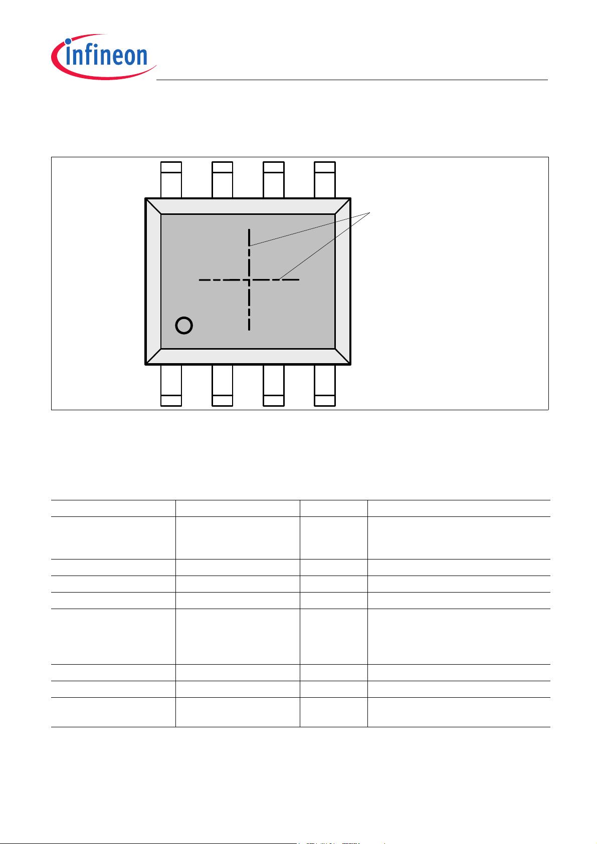
Figure 1-1 PG-DSO-8 package
1.1 Overview
The TLE5012B is a 360° angle sensor that detects the orientation of a magnetic field. This is achieved by
measuring sine and cosine angle components with monolithically integrated Giant Magneto Resistance (iGMR)
elements. These raw signals (sine and cosine) are digitally processed internally to calculate the angle orientation
of the magnetic field (magnet).
The TLE5012B is a pre-calibrated sensor. The calibration parameters are stored in laser fuses. At start-up the
values of the fuses are written into flip-flops, where these values can be changed to application-specific
parameters. The precision of the angle measurement, over a wide temperature range and a long lifetime, can be
improved by enabling an optional internal autocalibration algorithm.
Data communications are accomplished with a bi-directional Synchronous Serial Communication (SSC) that is
SPI-compatible. The sensor configuration is stored in registers, which are accessible by the SSC interface.
Additionally four other interfaces are available with the TLE5012B: Pulse-Width-Modulation (PWM) Protocol,
Short-PWM-Code (SPC) Protocol, Hall Switch Mode (HSM) and Incremental Interface (IIF). These interfaces can
be used in parallel with SSC or alone. Pre-configured sensor derivates with different interface settings are also
available. See the derivate ordering codes in the TLE5012B Data Sheet. A description of the derivates can also
be seen in Chapter 7.
Online diagnostic functions are provided to ensure reliable operation.
User’s Manual 9 Rev. 1.2, 2018-02

TLE5012B
M
Product Description
1.2 Features
• Giant Magneto Resistance (GMR)-based principle
• Integrated magnetic field sensing for angle measurement
• 360° angle measurement with revolution counter and angle speed measurement
• Two separate highly accurate single bit SD-ADC
• 15 bit representation of absolute angle value on the output (resolution of 0.01°)
• 16 bit representation of sine / cosine values on the interface
• Max. 1.0° angle error over lifetime and temperature-range with activated auto-calibration
• Bi-directional SSC Interface typ. 8Mbit/s
• Supports Safety Integrity Level (SIL) with diagnostic functions and status information
• Interfaces: SSC, PWM, Incremental Interface (IIF), Hall Switch Mode (HSM), Short PWM Code (SPC, based
on SENT protocol defined in SAE J2716)
• Output pins can be configured (programmed or pre-configured) as push-pull or open-drain
• Bus mode operation of multiple sensors on one line is possible with SSC or SPC interface in open-drain
configuration
•0.25 μm CMOS technology
• Automotive qualified: -40°C to 150°C (junction temperature)
• ESD > 4kV (HBM)
• RoHS compliant (Pb-free package)
• Halogen-free
1.3 Application Example
The TLE5012B GMR-based angle sensor is designed for angular position sensing in automotive applications such
as:
• Electrically commutated motor (e.g. Electric Power Steering (EPS), Brushless DC electric motors (BLDC))
• Rotary switches
• Steering angle measurements
• General angular sensing
The TLE5012B is also used in various non-automotive applications.
Figure 1-2 A usual application for TLE5012B is the electrically commutated motor
User’s Manual 10 Rev. 1.2, 2018-02

TLE5012B
VRG VRA VRD
TLE5012B
V
DD
X
GMR
Y
GMR
Temp
SD-
ADC
SD-
ADC
SD-
ADC
Digital
Signal
Processing
Unit
CORDIC
CCU
RAM
SSC Interface
Incremental IF
PWM
HSM
SPC
CSQ
SCK
DATA
IFA
IFB
GND
IFC
Osc PLL
ISM
Fuses
2 Functional Description
2.1 Block Diagram
Functional Description
Figure 2-1 TLE5012B block diagram
2.2 Functional Block Description
2.2.1 Internal Power Supply
The internal stages of the TLE5012B are supplied with several voltage regulators:
• GMR Voltage Regulator, VRG
• Analog Voltage Regulator, VRA
• Digital Voltage Regulator, VRD (derived from VRA)
These regulators are directly connected to the supply voltage V
2.2.2 Oscillator and PLL
The digital clock of the TLE5012B is provided by the Phase-Locked Loop (PLL), which is by default fed by an
internal oscillator. In order to synchronize the TLE5012B with other ICs in a system, the TLE5012B can be
User’s Manual 11 Rev. 1.2, 2018-02
.
DD

TLE5012B
DSPU
RAM
F
U
S
E
GND
0
F
U
S
E
GND
…
V
DD
0
V
DD
DSPU
RAM
F
U
S
E
GND
F
U
S
E
GND
…
0
V
DD
0
V
DD
DSPU
RAM
GND
F
U
S
E
GND
…
10
0
V
DD
1
V
DD
Functional Description
configured via SSC interface to use an external clock signal supplied on the IFC pin as the PLL source, instead of
the internal clock. External clock mode is only available in the PWM or SPC interface configurations.
2.2.3 SD-ADC
The Sigma-Delta Analog-Digital-Converters (SD-ADC) transform the analog GMR voltages and temperature
voltage into the digital domain.
2.2.4 Digital Signal Processing Unit
The Digital Signal Processing Unit (DSPU) contains the:
• Intelligent State Machine (ISM), which does error compensation of offset, offset temperature drift, amplitude
synchronicity and orthogonality of the raw signals from the GMR bridges, and performs additional features
such as auto-calibration, prediction and angle speed calculation
• COordinate Rotation DIgital Computer (CORDIC), which contains the trigonometric function for angle
calculation
• Capture Compare Unit (CCU), which is used to generate the PWM and SPC signals
• Random Access Memory (RAM), which contains the configuration registers
• Laser Fuses, which contain the calibration parameters for the error-compensation and the IC default
configuration, which is loaded into the RAM at startup
Laser fuses configuration
The laser fuse settings are derivate specific. During production, each and every TLE5012B chip is specifically
configured according to a derivate interface (PWM, SPC, HSM or IIF) and to its specific calibration values (e.g.
offset, amplitude synchronicity, orthogonality). These default values are set by laser fuses, where they remain
stored permanently. At power-on the values stored in the fuses are loaded into flip-flops (placed in the RAM).
Via the SSC interface, these derivate specific configuration values can be overwritten in the RAM. This allows
some programmability such as change of interface (using a IIF derivate as a PWM derivate for example) or to
correct the calibration values (if running the autocalibration mode for example). It is highly recommended to
configure the sensor with customized settings right after a Hardware reset (within the first 120µs, prior to start of
the Built-In Self-Test). If this interval is not sufficient, it is also possible to configure the sensor after the power-on
time. To ensure a correct configuration after power-on time, see recommendations on Chapter 6. When powered
off or reset, the overwritten values will be lost and the default values stored in the fuses will be reloaded into the
RAM at the next power up.
The Figure 2-2 shows how the fuse burning process works. In the original state all fuses are connected to ground
(GND). Once the calibration and derivate specific values are calculated, the information is burned into the fuses,
so that some remain connected to GND (“low” or logical “0”) and some are now pulled up by a resistor (“high” or
logical “1”). When powering the sensor, the RAM is initialized with the values from the fuses.
Figure 2-2 Laser Fuses burning process
User’s Manual 12 Rev. 1.2, 2018-02

TLE5012B
Functional Description
2.2.5 Interfaces
Bi-directional communication with the TLE5012B is enabled by a three-wire SSC interface. In parallel to the SSC
interface, one secondary interface can be selected, which is available on the IFA, IFB, IFC pins:
•PWM
• Incremental Interface
• Hall Switch Mode
• Short PWM Code
By using pre-configured derivates (see Chapter 7), the TLE5012B can also be operated with the secondary
interface only, without SSC communication.
2.2.6 Safety Features
The TLE5012B offers a multiplicity of safety features to support the Safety Integrity Level (SIL). Infineon’s sensors
that are intended for this purpose are identified by the following logo:
Figure 2-3 PRO-SIL
Disclaimer
PRO-SIL™ is a Registered Trademark of Infineon Technologies AG.
The PRO-SIL™ Trademark designates Infineon products which contain SIL Supporting Features.
SIL Supporting Features are intended to support the overall System Design to reach the desired SIL (according
to IEC61508) or A-SIL (according to ISO26262) level for the Safety System with high efficiency.
SIL respectively A-SIL certification for such a System has to be reached on system level by the System
Responsible at an accredited Certification Authority.
SIL stands for Safety Integrity Level (according to IEC 61508)
A-SIL stands for Automotive-Safety Integrity Level (according to ISO 26262)
Safety features are:
• Test vectors switchable to ADC input (activated via SSC interface)
• Inversion or combination of filter input streams (activated via SSC interface)
• Data transmission check via 8-bit Cyclic Redundancy Check (CRC) for SSC communcation and 4-bit CRC
nibble for SPC interface
• Built-in Self-test (BIST) routines for ISM, CORDIC, CCU, ADCs performed at startup
• Two independent active interfaces possible
• Overvoltage and undervoltage detection
TM
Logo
User’s Manual 13 Rev. 1.2, 2018-02

TLE5012B
V
DD
GNDADCX+
GMR Resistors
ADCX-ADC
Y
+ADCY-
V
X
V
Y
0°
N
S
90°
Functional Description
2.3 Sensing Principle
The Giant Magneto Resistance (GMR) sensor is implemented using vertical integration. This means that the
GMR-sensitive areas are integrated above the logic part of the TLE5012B device. These GMR elements change
their resistance depending on the direction of the magnetic field.
Four individual GMR elements are connected to one Wheatstone sensor bridge for each of the two components
of the applied magnetic field:
• X component, V
• Y component, V
With this full-bridge structure the maximum GMR signal is available and temperature effects cancel out each other.
(cosine) and the
x
(sine)
y
Figure 2-4 Sensitive bridges of the GMR sensor (not to scale)
Attention: Due to the rotational placement inaccuracy of the sensor IC in the package, the sensors 0°
position may deviate by up to 3° from the package edge direction indicated in Figure 2-4.
In Figure 2-4, the arrows in the resistors represent the magnetic direction which is fixed in the Reference Layer.
On top of the Reference Layer, and separated by a non magnetic layer, there is a Free Layer. When applying an
external magnetic field the Free Layer moves in the same direction as the external magnetic field, while the
Reference Layer remains fix. The resistance of the GMR elements depends on the magnetic direction difference
between the Reference Layer and the Free Layer.
When the external magnetic field is parallel to the direction of the Reference Layer, the resistance is minimal
(Reference Layer and Free Layer are parallel). When the external magnetic field and the Reference Layer are antiparallel (Reference Layer and Free Layer are anti-parallel), resistance is maximal.
The output signal of each bridge is only unambiguous over 180° between two maxima. Therefore two bridges are
oriented orthogonally to each other to measure 360°.
With the trigonometric function ARCTAN2, the true 360° angle value is calculated out of the raw X and Y signals
from the sensor bridges.
User’s Manual 14 Rev. 1.2, 2018-02

TLE5012B
V
Angle α
90° 180° 270° 360°0°
VX (COS)
Y Component (SIN)
VY (SIN)
V
Y
V
X
X Component (COS)
Figure 2-5 Ideal output of the GMR sensor bridges
Functional Description
User’s Manual 15 Rev. 1.2, 2018-02
TLE5012B
12 34
5678
Center of Sensitive
Area
2.4 Pin Configuration
Functional Description
Figure 2-6 Pin configuration (top view)
2.5 Pin Description
Table 2-1 Pin Description
Pin No. Symbol In/Out Function
1IFC
(CLK / IIF_IDX / HS3)
2 SCK I SSC Clock
3 CSQ I SSC Chip Select
4 DATA I/O SSC Data
5IFA
6V
7GND-Ground
8IFB
1) External clock feature is not available in IIF or HSM interface mode
(IIF_A / HS1 / PWM / SPC)
DD
(IIF_B / HS2)
I/O Interface C:
External Clock
Signal 3
I/O Interface A:
IIF Phase A / Hall Switch Signal 1 /
PWM / SPC output (input for SPC trigger
only)
- Supply Voltage
O Interface B:
IIF Phase B / Hall Switch Signal 2
1)
/ IIF Index / Hall Switch
User’s Manual 16 Rev. 1.2, 2018-02

TLE5012B
TLE5012B
CSQ
SCK
DATA
IFA
IFB
IFC
GND
VDD
3.0 – 5.5V
Rs1
SSC
IIF
100nF
(IIF_A)
(IIF_B)
(IIF_IDX)
Rs1
Rs2
Rs1 recommended, e.g. 100
Rs2 recommended, e.g. 470
TLE5012B
CSQ
SCK
DATA
IFA
IFB
IFC
GND
VDD
3.0 – 5.5V
Rs1
SSC
HSM
100nF
(HS1)
(HS2)
(HS3)
Rs1
Rs2
Rs1 recommended, e.g. 100
Rs2 recommended, e.g. 470
Application Circuits
3 Application Circuits
The application circuits in this chapter show the various communication possibilities of the TLE5012B. The pin
output mode configuration is device-specific and it can be either push-pull or open-drain. The bit IFAB_OD
(register IFAB, 0DH) indicates the output mode for the IFA, IFB and IFC pins. The SSC pins are by default pushpull (bit SSC_OD, register MOD_3, 09H). Every application circuits below are using otherwise specified SSC with
push-pull configuration and the internal clock.
3.1 IIF interface and SSC (IIF in push-pull configuration)
Figure 3-1 shows a block diagram of a TLE5012B with Incremental Interface (IIF) and SSC interface. The derivate
TLE5012B - E1000 is by default configured with push-pull IFA (IIF_A), IFB (IIF_ B) and IFC (IIF_IDX) pins. When
the output pins are configurated as open-drain, three pull-up resistors should be added (e.g. 2k2Ω) between the
data lines and VDD.
Figure 3-1 Application circuit for TLE5012B with IIF interface and SSC
3.2 HSM interface and SSC (HSM in push-pull configuration)
Figure 3-2 shows a block diagram of the TLE5012B with Hall Switch Mode (HSM) and SSC interface. The derivate
TLE5012B - E3005 is by default configurated with push-pull IFA (HS1), IFB (HS2) and IFC (HS3) pins.
Figure 3-2 Application circuit for TLE5012B with HSM interface (push-pull configuration) and SSC
User’s Manual 17 Rev. 1.2, 2018-02

TLE5012B
TLE5012B
CSQ
SCK
DATA
IFA
IFB
IFC
GND
VDD
3.0 – 5.5V
Rs1
SSC
HSM
100nF
(HS1)
(HS2)
(HS3)
Rs1
Rs2
Rs1 recommended, e.g. 100
Rs2 recommended, e.g. 470
Rpu
Rpu
Rpu
Rp u re q uir ed, e. g. 2K2
TLE5012B
CSQ
SCK
DATA
IFA
IFB
IFC
GND
VDD
3.0 – 5.5V
100nF
(PWM)
Rpd recommended, e.g. 10k
PWM
Application Circuits
3.3 HSM interface and SSC (HSM in open-drain configuration)
As shown in Figure 3-3 when IFA, IFB and IFC are configurated via the SSC interface as open drain pins, three
pull-up resistors (Rpu) should be added on the output lines.
Figure 3-3 Application circuit for TLE5012B with HSM interface (open-drain configuration) and SSC
3.4 PWM interface (push-pull configuration)
The TLE5012B can be configured with PWM only (Figure 3-4). The derivate TLE5012B - E5000 is by default
configurated with push-pull configuration for IFA (PWM) pin. Internal pull-up resistors are always available for
DATA and CSQ pins (see Datasheet). It is recommended to connect CSQ pin to V
avoid unintentional activation of the SSC interface. DATA pin should be left open. The figure below shows a typical
implementation of the TLE5012B - E5000.
Figure 3-4 Application circuit for TLE5012B with PWM (push-pull configuration) interface
User’s Manual 18 Rev. 1.2, 2018-02
to provide a high level and
DD

TLE5012B
TLE5012B
CSQ
SCK
DATA
IFA
IFB
IFC
GND
VDD
3.0 – 5.5V
100nF
(PWM)
Rpd recommended, e.g. 10k
Rpu required, e.g. 2K2
PWM
Rpu
TLE5012B
CSQ
SCK
DATA
IFA
IFB
IFC
GND
VDD
3.0 – 5.5V
100nF
(SPC)
Rpd recommended, e.g. 10k
Rpu required, e.g. 2K2
SPC
Rpu
Application Circuits
3.5 PWM interface (open-drain configuration)
The TLE5012B - E5020 is also a PWM derivate but with open drain for IFA (PWM) pin. A pull-up resistor (e.g.
2.2kΩ) should be added between the IFA line and VDD, as shown in Figure 3-5.
Internal pull-up resistors are always available for DATA and CSQ pins (see Datasheet). It is recommended to
connect CSQ pin to V
pin should be left open. The figure below shows a typical implementation of the TLE5012B - E5020.
to provide a strong level and avoid unintentional activation of the SSC interface. DATA
DD
Figure 3-5 Application circuit for TLE5012B with PWM (open-drain configuration) interface
3.6 SPC interface
The TLE5012B can be configured with SPC only (Figure 3-6). This is only possible with the TLE5012B - E9000
derivate, which is by default configurated with an open-drain IFA (SPC) pin.
In Figure 3-6 the IFC (S_NR[1]) and SCK (S_NR[0]) pins are set to ground to generate the slave number (S_NR)
0
(or 00B). In case of SCK (S_NR[0]) needs to be set to VDD to generate another slave address, CSQ pin should
D
be set to ground instead. Internal pull-up resistors are always available for DATA and CSQ pins (see Datasheet).
DATA pin should be left open. Since SCK and CSQ pins should have opposite level, it is not recommended to use
the SSC interface in parallel.
Figure 3-6 Application circuit for TLE5012B with SPC interface
User’s Manual 19 Rev. 1.2, 2018-02

TLE5012B
Shift Reg.
Shift Reg.
Clock Gen.
DATA
MTSR
MRST
SCK
SCK
(SSC Slave) TLE 5012B µC (SSC Master)
CSQ CSQ
EN
EN
Rs1 recommended, e.g. 100
Rs2 recommended, e.g. 470
Rs1
Rs1
Rs2
Shift Reg.
Shift Reg.
Clock Gen.
DATA
MTSR
MRST
SCK
SCK
(SSC Slave) TLE 5012B µC (SSC Master)
CSQ CSQ
Rs1 recommended, e.g. 100
Rpu required, e.g. 1k
Rs1
Rs1
Rs1 Rs1
Rpu
EN
EN
Application Circuits
3.7 SSC interface (push-pull configuration)
In Figure 3-1, Figure 3-2 and Figure 3-3 the SSC interface has the default push-pull configuration (see details in
Figure 3-7). A series resistor on the DATA line is recommended to limit the current in erroneous cases (e.g. the
sensor pushes high and the microcontroller pulls low at the same time or vice versa). Resistors on SCK and CSQ
lines are recommended in case of disturbances or noise.
Figure 3-7 SSC interface with push-pull configuration (high-speed application)
3.8 SSC interface (open-drain configuration)
It is possible to use an open-drain configuration for the DATA line. This setup can be used to communicate with a
microcontroller in a bus system, together with other SSC slaves (e.g. two TLE5012B devices for redundancy
reasons). This mode can be activated using the bit SSC_OD.
Even though, push-pull configuration in a bus system is also possible since the addressing of the sensor is
perfomed with CSQ pin.
The open-drain configuration can be seen in Figure 3-8. Series resistors on the DATA line are recommended to
limit the current in erroneous cases. Resistors on SCK and CSQ lines are recommended in case of disturbances
or noise A pull-up resistor of typ. 1 kΩ is required on the DATA line.
Figure 3-8 SSC interface with open-drain configuration (bus systems)
User’s Manual 20 Rev. 1.2, 2018-02

TLE5012B
Sensor 1
OUT
VDD
VDD
CCU
VDD
GND
VDD
GND
MCU
VDD
Rpu
VDD
Sensor x
OUT
VDD
GND
Application Circuits
3.9 Sensor supply in bus mode
When using two or more devices in a bus configuration (SSC or SPC interface). It is recommended to use the
same supply for every sensors connected to the bus. In case of a power loss the unpowered device is sinking
current through the OUT pin. Depending on the external circuitry the additional current flow might disturb the bus
behavior.
The figure below (Figure 3-9) shows a typical implementation of a bus mode using SPC interface. External
components such as EMC filter or additional series resistors are not represented for clarity purpose. Only the pullup resistor Rpu is shown.
Figure 3-9 Sensors’ supply in bus mode
User’s Manual 21 Rev. 1.2, 2018-02

TLE5012B
Fused Offsets:
X_Offset: -633
Y_Offset: -653
Acquire
Max-Min
pairs
Calculate:
Offs ets, Synch
X_Offset: -646
Y_Offset: -658
Acquire
Max-Min
pairs
Calculate:
Offs ets, Synch
X_Offset: -651
Y_Offset: -664
Tempe-
rature
Check
Tempe-
rature
Check
Parameters
Correct ion
Parameters
Correction
-633
-646
-651
-653
-658
-664
-670
-665
-660
-655
-650
-645
-640
-635
-630
-625
-620
Offset
Filter update period (t
upd
)
X_Offset Y_Offset
Parameters Correction
Acquire MaxMin pairs
Parameters
Correction
Acquire Max-Min pairs
-633
-634
-635
-653
-654
-655
-660
-655
-650
-645
-640
-635
-630
-625
-620
01234
Revolutions
X_Offset Y_Offset
Parameters
Correction
Acquire Max-Min
pairs
Parameters
Correction
Acquire Max-Min pairs
Fused Offsets:
X_Offset: -633
Y_Offset: -653
Acquire
Max-Min
pairs
Calculate:
Offs ets, Synch
X_Offset: -646
Y_Offset: -658
Acquire
Max-Min
pairs
Calculate:
Offs ets, Synch
X_Offset: -651
Y_Offset: -664
Tempe-
rature
Check
Tempe-
rature
Check
Parameters
Correct ion
by only 1
LSB
Parameters
Correction
Offset
Specification
4 Specification
4.1 Autocalibration
Autocalibration enables online parameter calculation, and therefore reduces angle error due to temperature and
lifetime drifts.
The TLE5012B is a pre-calibrated sensor; at start-up the parameters stored in the laser fuses are loaded into flipflops. During operation, the TLE5012B needs 1.5 revolutions to generate new autocalibration parameters. The
parameters are updated with new autocalibration parameters according to the mode selected via the AUTOCAL
bits (Mode 2 register). The parameters are updated in a smooth way to avoid an angle jump on the output; only
one Least-Significant Bit (LSB) will be changed within the chosen range or time. Once the parameters are updated,
a new autocalibration parameter generation starts, as autocalibration is done continuously.
AUTOCAL Modes:
• 00: No autocalibration
• 01: Autocalibration Mode 1. Parameters are updated by one LSB at every update time t
FIR_MD setting) till the new autocalibration parameter values are reached.
• 10: Autocalibration Mode 2. Parameters are updated by one LSB only. After the update, autocalibration will
already calculate new parameters again.
• 11: Autocalibration Mode 3. Parameters are updated by one LSB at every angle range of 11.25° till the new
autocalibration parameter values are reached.
(dependent on
upd
Figure 4-1 Parameter correction with autocalibration mode 1
Figure 4-2 Parameter correction with autocalibration mode 2
User’s Manual 22 Rev. 1.2, 2018-02

TLE5012B
-633
- 646
-651
- 653
-658
- 664
-670
-665
-660
-655
-650
-645
-640
-635
-630
-625
-620
Angle [°]
X_Offset Y_Offset
Parameters Correction
Acquire Max-Min
pairs
Parameters
Correction
Acquire Max-Min pairs
Fused Offsets:
X_Offset: -633
Y_Offset: -653
Acquire
Max-Min
pairs
Calculate:
Offs ets, Synch
X_Offset: -646
Y_Offset: -658
Acquire
Max-Min
pairs
Calculate:
Offs ets, Synch
X_Offset: -651
Y_Offset: -664
Tempe -
rature
Check
Tempe-
rature
Check
Parameters
Correct ion
Parameters
Correction
Offset
Specification
Figure 4-3 Parameter correction with autocalibration mode 3
The autocalibration mode 1 is the quickest mode to correct the parameters. Mode 2 is the slowest method, but
since the parameters are updated by one digit only, it offers robustness against corrupted maxima - minima pair
(in case of a spike, for example).
Condition for usability of Autocalibration:
The autocalibration algorithm relies on the collection of maximum and minimum values of the raw X- and Y-signals
of the sensing elements, therefore it is suitable for applications where a rotor is continuously turning (full 360°
rotations). Compensation parameters for offset and amplitude synchronicity error are calculated from these
minima and maxima only if the temperature did not change by more than 5 Kelvin during their collection, to avoid
temperature-drift induced errors.
For the sensor to be accurate in autocalibration mode, it has to be assured in the application that the calibration
parameters are updated frequently. Thus, autocalibration should only be used in applications where the magnet
regularly rotates by at least one full turn (internal TLE5012B check of full turn requires maximum 1.5 revolutions)
at a temperature which is constant within 5 Kelvin.
Enabling/Disabling of Autocalibration:
When switching autocalibration on or off, the TLE5012B may erroneously trigger the S_FUSE error bit in the status
register, which indicates a configuration CRC error, which is also displayed permanently in the Safety Word of the
SSC communication.
When autocalibration is ON and has to be disabled: write the correct CRC for autocalibration OFF before disabling
autocalibration. This way the sensor will see a consistent state when the first runtime CRC check is done again
and no CRC error will occur. The correct CRC must be calculated on the microcontroller side.
When autocalibration is OFF and has to be enabled or just restarted: after switching the autocalibration mode ON,
the Status Register should be read via SSC after three t
periods and an occurring S_FUSE error should be
update
ignored.
Changing TLE5012B default Configuration, if Autocalibration is enabled
Changing certain TLE5012B default configurations while autocalibration is enabled could lead to corrupted
autocalibration parameters. Therefore, disable autocalibration prior to change the angle direction (ANG_DIR bit
on MOD_2 register), prediction (PREDICT bit on MOD_2 register) or the angle base (ANG_BASE bits on MOD_3
register). Once these parameters have been changed, enable autocalibration again.
An initialization sequence for the case of changing angle direction is shown in Table 4-1. This sequence is also
valid for prediction and for angle base. In case of angle base additonal write after the first write is required in order
to re-configure the new angle base value.
User’s Manual 23 Rev. 1.2, 2018-02

TLE5012B
Specification
Table 4-1 Initialization via SSC / SPI to change ANG_DIR
Step Command type Register Value Description
0 (default) - MOD_2 0x0801 Angle Range = 360°, Angle Direction = counter clockwise,
Autocal = on
This is the default value.
1 W (write) MOD_2 0x0808 Angle Range = 360°, Angle Direction = clockwise, Autocal =
off
Autocal is being deactivated, and Angle direction can be
changed. The deactivated autocal stops any running
min/max search and clears the min/max_x/y registers before
any offset (and amplitude) parameters can change.
2 Wait - 128µs A minimum of two t
periods are needed until all settings
update
have been adopted by the sensor. Since this delay depends
on the timing of the SPI write in comparison to the sensors
internal execution timing it is recommended to wait three
t
(3*42.7µs by default) for time margin. In case t
update
update
is
configured to 85µs (or higher), extend the time to fulfill
3*t
update
.
This waiting time is also important before reading the default
parameters (OFFX, OFFY, SYNCH, IFAB, MOD4, TCO_Y,
T25O) in case it is necessary.
3 W MOD_2 0x0809 Angle Range = 360°, Angle Direction = clockwise, Autocal =
on
Angle direction has been changed previously and now
autocal is again activated.
4 Wait - 128µs Similar to wait above. Sensor needs time to recognize that
the CRC check of the parameter registers (Addresses
0x08...0x0F) need to be disabled due to reactivated autocal.
5 R (read) STAT S_FUSE
error
S_FUSE error may be present due to reconfiguration (as
explained on Note on Page 23). Reading out the STAT
register the S_FUSE is reset (SPI Safety Word will not show
anymore an error because it has been cleared).
6 R STAT S_FUSE
cleared
This read is only necesary if the previosu SPI Safety Word is
not checked for a system-error (includes S_FUSE).
User’s Manual 24 Rev. 1.2, 2018-02

TLE5012B
T
rpm
Additional
Ang le Er ror
OKOK OK
Specification
4.1.1 Angle Error adder with Autocalibration enabled
With constant temperatures (ΔT < 5 Kelvin) or parts rotating faster than the temperature changes, the
autocalibration angle error is as specified in the TLE5012B Data Sheet. If autocalibration is enabled when the
temperature changes by more than 5 Kelvin within 1.5 revolutions, the last valid autocalibration parameters will
still be used, leading to an additional angle error. Such cases will happen when the rotating part is halted and the
temperature is changing by more than 5 Kelvin or the rotating part is moving too slowly compared to the external
temperature changes (see Figure 4-4).
Figure 4-4 Cases where an angle error adder has to be included if autocalibration is enabled
The angle error adder is described in the TLE5012B Data Sheet (Figure 4-3, page #25 on the TLE5012B Data
Sheet, Rev. 2.0 from 2014-02) and depends on the initial temperature. To read the right angle error adder select
the initial temperature and move through the x-axis as many degrees as the delta between the final temperature
and the initial temperature. Then read the y-axis value at this delta and add it to the specified angle error, which
already contains lifetime drifts. Some cases are shown in Table 4-2:
Table 4-2 Additional angle error examples
T
range Autocal T/1.5 revolutions Additional angle error
junction
-40°C ... 150°C Off - No additional angle error
-40°C ... 150°C On < 5 Kelvin No additional angle error
-40°C ... 150°C On 10 Kelvin <0.2°
-40°C ... 150°C On 20 Kelvin <0.35°
-40°C ... 150°C On 50 Kelvin <0.85°
>135°C On 15 Kelvin <3.3°
As the magnetic field decreases with higher temperatures, angle errors due to increases of temperature are more
critical than decreases of temperature. As the additional angle error described in the TLE5012B Data Sheet
applies to the worst case (temperature increasing), the angle error adder due to decreasing temperature changes
will always be smaller.
If a parallel SSC interface is in place, autocalibration can be disabled when a critical case described in Figure 4-4
occurs. A temperature check in the microcontroller can be implemented to disable and enable autocalibration (and
thus to reset any wrong minima and maxima) on temperature changes by more than 5 Kelvin during 1.5
revolutions. When autocalibration is disabled the default calibration parameters stored in the laser fuses will be
used for the X and Y raw values correction, and the angle error will fulfill the specifications described in the
TLE5012B Data Sheet.
User’s Manual 25 Rev. 1.2, 2018-02
TLE5012B
)2()1()()1(
tttt
ααα
α
time
Angle
With
Prediction
Without
Prediction
t
adel
t
upd
Magnetic field
direction
Sensor output
Prediction
Angle
Value
Revolution
counter
Angle
Value
Revolution
counter
Angle
Value
Revolution
counter
Regi ster MOD_ 2; 08
H
AVAL; 02
H
AREV; 04
H
AVAL; 02
H
AREV; 04
H
AVAL; 02
H
AREV; 04
H
Field PREDICT [2] ANG_VAL [14:0] REVOL [8:0] ANG_VAL [14:0] REVOL [8:0] ANG_VAL [14:0] REVOL [8:0]
Without
prediction
0 3 43 1 43 359 42
With
prediction
1 1 43 359 43 357 42
0°
0°
0°
Specification
4.2 Prediction mode
The TLE5012B has an optional prediction feature, which serves to reduce the speed dependent angle error in
applications where the rotation speed does not change abruptly. Prediction (enable PREDICT bit on MOD_2
register) uses the difference between current and last two angle values to approximate the angle value which will
be present after the delay time (see Figure 4-5). The output value is calculated by adding this difference to the
measured value, according to Equation (4.1).
−−−+=+
(4.1)
Figure 4-5 Delay of sensor output
Revolution counter on prediction mode
The revolution counter (REVOL bits on AREV register) counts full rotations of the magnetic field. It increments
when the measured angle crosses the 0° point in counter-clockwise rotation direction, and it decrements when the
0° point is crossed in clockwise rotation direction. The revolution counter always works with the measured angle
(current angle and not predicted angle). Therefore, the prediction angle may already indicate that the 0° has been
crossed but the revolution counter may still not increase or decrease if the current calculated angle has not yet
changed quadrant. Once the current calculated angle crosses 0°, the revolution counter will be updated. The
Figure 4-6 illustrates an example; in the second picture the angle value with prediction has already crossed the
0° (from 1° to 359°), but the revolution counter has not yet decreased (remains 43):
Figure 4-6 Revolution counter with prediction mode disabled/enabled
User’s Manual 26 Rev. 1.2, 2018-02

TLE5012B
)(
∑
×+××=×=Δ
Δ+=
Q
QQDDDDthJATOTthJA
AJ
thCAthJCthJA
IVIVRPRT
TTT
RRR
(IDD, IQ> 0, if direction is into IC)
[] [] [ ]
()
KVAAV
W
K
T
mAI
VV
DD
DD
5.100014.05150
14
5
=+××
⎥
⎦
⎤
⎢
⎣
⎡
=Δ
=
7281632128256
2*12*12*12*12*12*02*02*02*1
2*12*12*02*12*122
3457899897969
5949392919
2
0
1
−=++++−=
=++++−=++++
+++++−=∗+∗−=
−−−−
−−−−−
−
=
−
∑
N
i
i
i
N
MSB
bbValu e
C
Cdig
digdigTEMPER
CT °==
+
−
=
°
+
=° 8.28
776.2
80
776.2
15272
]/[776.2
][152][
][
][530][25][_][ digdigOTdigRAWTdigTEMPER
−
4.3 Calculation of the Junction Temperature
The total power dissipation P
above the ambient temperature.
The power multiplied by the total thermal resistance R
R
is the sum of the two components Junction to Case and Case to Ambient.
thJA
of the chip leads to self-heating, which increases the junction temperature T
TOT
(junction to ambient) yields the junction temperature.
thJA
+=
Example (assuming no load on V
out
):
=
Specification
J
(4.2)
(4.3)
4.4 Calculation of the Temperature
The TLE5012B provides the temperature in the TEMPER bits of the FSYNC register via the SSC interface (see
Chapter 6.2) or with an extended SPC frame (see Table 5-8). TEMPER is a compensated value of the
temperature at the ADC. The compensation is done with an offset value at 25°C temperature (T25O), which is
specific for each device. The T25O value is measured for each device during production and it is stored in the
fuses.
The temperature in degrees Celsius (°C) can be calculated using the formula provided in Chapter 6.2 and reading
the TEMPER bits. TEMPER is a signed register, to convert the value to digits proceed as described in
Chapter 6.1.3. As an example, for a TEMPER value of 110111000
Equation (4.4):
Therefore, the temperature in degrees Celsius is calculated in Equation (4.5):
, the value in digits is calculated in
B
(4.4)
(4.5)
TEMPER typical accuracy error is around +/-5°C across the whole temperature range.
TEMPER is a limited register. For a whole temperature range use the T_RAW register, which can be compensated
with the T25O register. The relation between TEMPER and T_RAW is shown in Equation (4.6):
User’s Manual 27 Rev. 1.2, 2018-02
−=
(4.6)

TLE5012B
Specification
4.5 Switching to external clock
External clock operation is possible for the interface configurations SSC only, SSC & PWM, and SSC & SPC. To
switch the TLE5012B to external clock supply the following procedure is used:
• Trigger a chip reset by writing a “1” to the AS_RST bit (address 01
• Within 120µs after the reset command, write a “1” to the CLK_SEL bit (address 06
• After the power-on time (max. 7 ms), read the CLK_SEL bit via SSC interface to confirm that external clock is
selected
Note: If the clock source (CLK_SEL) bit is switched to external clock during operation of the sensor it may occur
(at a chance of roughly 1%) due to an internal timing conflict, that the switching command is not accepted
and the chip keeps operating on internal clock.
[0]) via SSC interface
H
[4])
H
User’s Manual 28 Rev. 1.2, 2018-02

TLE5012B
Interfaces
5 Interfaces
5.1 Interfaces overview
The TLE5012B supports five interfaces which can be choosen depending on the specific application:
• SSC (Synchronous Serial Communication)
• PWM (Pulse Width Modulation)
• SPC (Short PWM Code)
• HSM (Hall Switch Mode)
• IIF (Incremental Interface)
SSC: the SSC is a digital interface which allows bi-directional data transfer. The TLE5012B uses 3-pin as
described in the Chapter 5.2. SSC allows to read additional data to the angle value from registers (angle speed,
raw values, temperature, etc.) and to setup different configurations (resolution, enable/disable of features such as
prediction or autocalibration, etc.). Check Chapter 6 for details. SSC allows a high data transfer with CRC (Cyclic
Redundancy Check) and secure communication (use of the Safety Word after data transfer). Up to 4 sensors can
be used with SSC. SSC is meant for short distances (TLE5012B and ECU to be placed on the same PCB)
PWM: the PWM is an unidirectional interface. Only one line is needed in which the angle value is transmitted. The
angle value corresponds to the duty cycle of the signal, with 0° represented by a 6.25% duty cycle and 93.75%
representing the maximum angle. Safety Analysis results would be communicatd via duty cycle below 2% or above
98%. The frequency of the PWM interface can be set via SSC interface. PWM is meant to support distances up
to 5 meters.
SPC: the SPC is an interface based on the SENT protocol. The ECU (master µC) sends a Trigger Nibble which
wakes up the TLE5012B to transmit the angle value (12bit or 16bit resolution depending on the number of nibbles).
If desired, the temperature can also be transmitted in two extra nibbles. The SPC also sends a CRC and an endpulse to terminate the communication. One line is needed for the transmission and the pins #1 and #2 are used
to set the slave number. Up to four slaves can be connected to one ECU; the ECU Trigger Nibble length will wake
up the respective sensor. SAE International describes the SENT protocol (SAE J2716) distance as up to 5 meters:
“Combined resistance for all connector shall have less than 1 Ohms per line over total vehicle life. The bus wiring
shall utilize cables with less than 0.1nF per meter of wire length. the maximum cable length shall be 5 meters”.
HSM: the HSM is an interface that emulates the output of three Hall switches, therefore three uni-directional lines
are required. Only the angle position can be calculated from the output. The switching hysteresis and the pole-pair
configuration can be selected via SSC. By default the number of pole pairs is set to 5.
IIF: the IIF is an interface that emulates an optical encoder. Three uni-directional lines are required: two for Phase
A and Phase B and a third one for the IIF Index (which indicates a 0° pass). Phase A and Phase B pulse out phaseshifted pulses for each “step resolution” that the angle moved. The two Phases are needed to also track the
rotation direction (clockwise or counter-clockwise). At start-up the IIF pulses out the angle value. Different IIF
modes, step resolutions and hysteresis values can be configurated via SSC. IIF interface is meant for short
distances (TLE5012B and ECU to be placed on the same PCB). It is used for high-speed applications such as
electrically commutated motor drives.
SSC can be used in parallel to any other interface (PWM, SPC, HSM or IIF).
More details on the default configuration of each derivate are described in Chapter 7.
User’s Manual 29 Rev. 1.2, 2018-02

TLE5012B
Interfaces
Table 5-1 summarizies the key characteristics and parameters that have to be considered when choosing an
interface:
Table 5-1 Main interface characteristics
Characteristics IIF PWM SPC HSM SSC
Data/Values angle steps
(angle value at
start-up)
Distance
1)
short-medium long (up to 5m) long (up to 5m) medium short
angle value angle value
(temperature
optional)
angle value
period
many data
available in the
registers
Data rate high low-medium low high high
Resolution high high high low high
Check IIF Index (0°
pulse). Phase
A/B as
complementary
signal.
Duty cycle range
diagnostics.
CRC HS1/HS2/HS3 as
complementary
signals.
Safety Word in
the data transfer.
Availability of
status and
diagnostics
registers.
Max. slaves in
no bus mode no bus mode 4 no bus mode 4
bus mode
Communication
2)
lines
Communication unidirectional unidirectional unidirectional
3 (only two
without IIF Index)
1133
unidirectional bidirectional
(triggered)
SSC possible Yes Yes Yes Yes Yes
Other Emulates Optical
Encoder
1) Not subject to production test. Distance subject to application circuit and environment.
2) Communication lines between slave (TLE5012B) and master (microcontroller). External clock not included
Based on SENT
protocol
Emulates (three)
Hall Switches
3-wire SPI
User’s Manual 30 Rev. 1.2, 2018-02

TLE5012B
SCK
t
CSs
t
SCKp
t
SCKh
t
CSh
CSQ
t
SCKl
t
CSoff
t
DATAs
DATA
t
DATAh
5.2 Synchronous Serial Communication (SSC) Interface
5.2.1 SSC Timing Definition
Figure 5-1 SSC timing
Interfaces
SSC Inactive Time (CS
off
)
The SSC inactive time defines the delay time after a transfer before the TLE5012B can be selected again.
Table 5-2 SSC push-pull timing specification
Parameter Symbol Values Unit Note / Test Condition
Min. Typ. Max.
1)
1)
1)
1)
1)
1)
1)
1)
1)
1)
1)
1)
SSC baud rate f
CSQ setup time t
CSQ hold time t
CSQ off t
SCK period t
SCK high t
SCK low t
DATA setup time t
DATA hold time t
Write read delay t
Update time t
SCK off t
1) Not subject to production test - verified by design/characterization
SSC
CSs
CSh
CSoff
SCKp
SCKh
SCKl
DATAs
DATAh
wr_delay
CSupdate
SCKoff
105 ns
105 ns
600 ns SSC inactive time
120 125 ns
40 ns
30 ns
25 ns
40 ns
130 ns
170 ns
8.0 Mbit/s
1 μsSee Figure 5-5
User’s Manual 31 Rev. 1.2, 2018-02

TLE5012B
Interfaces
Table 5-3 SSC open-drain timing specification
Parameter Symbol Values Unit Note / Test Condition
Min. Typ. Max.
SSC baud rate f
CSQ setup time t
CSQ hold time t
CSQ off t
SCK period t
SCK high t
SCK low t
DATA setup time t
DATA hold time t
Write read delay t
Update time t
SCK off t
SSC
CSs
CSh
CSoff
SCKp
SCKh
SCKl
DATAs
DATAh
wr_delay
CSupdate
SCKoff
300 ns
400 ns
600 ns SSC inactive time
500 ns
25 ns
40 ns
130 ns
170 ns
1) Not subject to production test - verified by design/characterization
2.0 Mbit/s Pull-up Resistor = 1k
1)
1)
1)
190 ns
190 ns
1)
1)
1)
1)
1)
1 μsSee Figure 5-5
1)
1)
1)
1)
User’s Manual 32 Rev. 1.2, 2018-02

TLE5012B
COMMAND READ Data 1 READ Data 2
SAFETY-WORD
SSC-Master is driving DATA
SSC-Slave is driving DATA
t
wr_delay
COMMAND WRITE Data 1
SAFETY-WORD
SSC-Master is driving DATA
SSC-Slave is driving DATA
t
wr_delay
5.2.2 SSC Data Transfer
The SSC data transfer is word-aligned. The following transfer words are possible:
• Command Word (to access and change operating modes of the TLE5012B)
• Data words (any data transferred in any direction)
• Safety Word (confirms the data transfer and provides status information)
Figure 5-2 SSC data transfer (data-read example)
Interfaces
Figure 5-3 SSC data transfer (data-write example)
Command Word
SSC Communication between the TLE5012B and a microcontroller is generally initiated by a command word. The
structure of the command word is shown in Table 5-4, where the Update (UPD) bit allows the access to current
values or updated values. If an update command is issued and the UPD bit is set, the immediate values are stored
in the update buffer simultaneously. This enables a snapshot of all necessary system parameters at the same
time. Bits with an update buffer are marked by an “u” in the Type column in register descriptions. The initialization
of such an update is described on page 35.
Table 5-4 Structure of the Command Word
Name Bits Description
RW [15] Read - Write
0: Write
1: Read
Lock [14..11] 4-bit Lock Value
0000
0x30
1010
: Default operating access for addresses 0x00:0x04, 0x14:0x15, 0x20,
B
: Configuration access for addresses 0x05:0x11
B
User’s Manual 33 Rev. 1.2, 2018-02

TLE5012B
Interfaces
Table 5-4 Structure of the Command Word (cont’d)
Name Bits Description
UPD [10] Update-Register Access
0: Access to current values
1: Access to values in update buffer
ADDR [9..4] 6-bit Address
ND [3..0] 4-bit Number of Data Words (if bits set to 0000
, no safety word is provided)
B
Safety Word
The safety word consists of the following bits:
Table 5-5 Structure of the Safety Word
Name Bits Description
1)
STAT
Chip and Interface Status
[15] Indication of chip reset or watchdog overflow (resets after readout) via SSC
0: Reset occurred
1: No reset
[14] System error (e.g. overvoltage; undervoltage; V
-, GND- off; ROM;...)
DD
0: Error occurred (S_VR; S_DSPU; S_OV; S_XYOL: S_MAGOL; S_FUSE;
S_ROM; S_ADCT)
1: No error
[13] Interface access error (access to wrong address; wrong lock)
0: Error occurred
1: No error
[12] Invalid angle value (NO_GMR_A = 1; NO_GMR_XY = 1)
0: Angle value invalid
1: Angle value valid
RESP [11..8] Sensor number response indicator
The sensor number bit is pulled low and the other bits are high (one-cold
encoding, e.g. for the sensor -or slave- number “00” the RESP bits are
“1110”. For the sensor -or slave- number “10” the RESP bits are “1011”).
CRC [7..0] Cyclic Redundancy Check (CRC), which includes the STAT and RESP bits.
1) When an error occurs, the corresponding status bit in the safety word remains “low” until the STAT register (address 00H)
is read via SSC interface. Once the STAT register has been read, the safety word status bits will be “high” again.
Bit Types
The types of bits used in the registers are listed here:
Table 5-6 Bit Types
Abbreviation Function Description
r Read Read-only registers
w Write Read and write registers
u Update Update buffer for this bit is present. If an update is issued and the Update-
Register Access bit (UPD in command word) is set, the immediate values are
stored in this update buffer simultaneously. This allows a snapshot of all
necessary system parameters at the same time.
User’s Manual 34 Rev. 1.2, 2018-02

TLE5012B
SCK
DATA 811 10 9MSB 14 13 12
CSQ
SSC T ransfer
LSB3217 6 5 4
Com m and W or d
Data Word (s)
SSC -Mas ter i s dri ving D AT A
SSC -Slave i s dri ving D AT A
LSB1
RW ADDR LENGTHLOC K
MSB
t
wr_delay
UPD
SCK
DATA
CSQ
LSB LSBMSB
Com mand Word Data Word (s)Update -Signal
Update - Event
SSC -M aster is dr i v ing DAT A
SSC -Slave is driving DAT A
t
CSupdate
Data communication via SSC
Figure 5-4 SSC bit ordering (read example)
Interfaces
Figure 5-5 Update of update registers
The data communication via SSC interface has the following characteristics:
• The data transmission order is Most-Significant Bit (MSB) first, Least-Significant Bit (LSB) last.
• Data is put on the data line with the rising edge of SCK and read with the falling edge of SCK.
• The SSC Interface is word-aligned. All functions are activated after each transmitted word.
• After every data transfer with ND 1, the 16-bit Safety Word is appended by the TLE5012B.
• A “high” condition on the Chip Select pin (CSQ) of the selected TLE5012B interrupts the transfer immediately.
The CRC calculator is automatically reset.
• After changing the data direction, a delay t
data transfer. This is necessary for internal register access.
• If in the Command Word the number of data is greater than 1 (ND > 1), then a corresponding number of
consecutive registers is read, starting at the address given by ADDR.
• In case an overflow occurs at address 3F
• If in the Command Word the number of data is zero (ND = 0), the register at the address given by ADDR is
read, but no Safety Word is sent by the TLE5012B. This allows a fast readout of one register.
• At a rising edge of CSQ without a preceding data transfer (no SCK pulse, see Figure 5-5), the content of all
registers which have an update buffer is saved into the buffer. This procedure serves to take a snapshot of all
relevant sensor parameters at a given time. The content of the update buffer can then be read by sending a
read command for the desired register and setting the UPD bit of the Command Word to “1”.
• After sending the Safety Word, the transfer ends. To start another data transfer, the CSQ has to be deselected
once for at least t
• By default, the SSC interface is set to push-pull. The push-pull driver is active only if the TLE5012B has to send
data, otherwise the DATA pin is set to high-impedance.
User’s Manual 35 Rev. 1.2, 2018-02
(see Table 5-3) has to be implemented before continuing the
wr_delay
, the transfer continues at address 00H.
H
.
CSoff
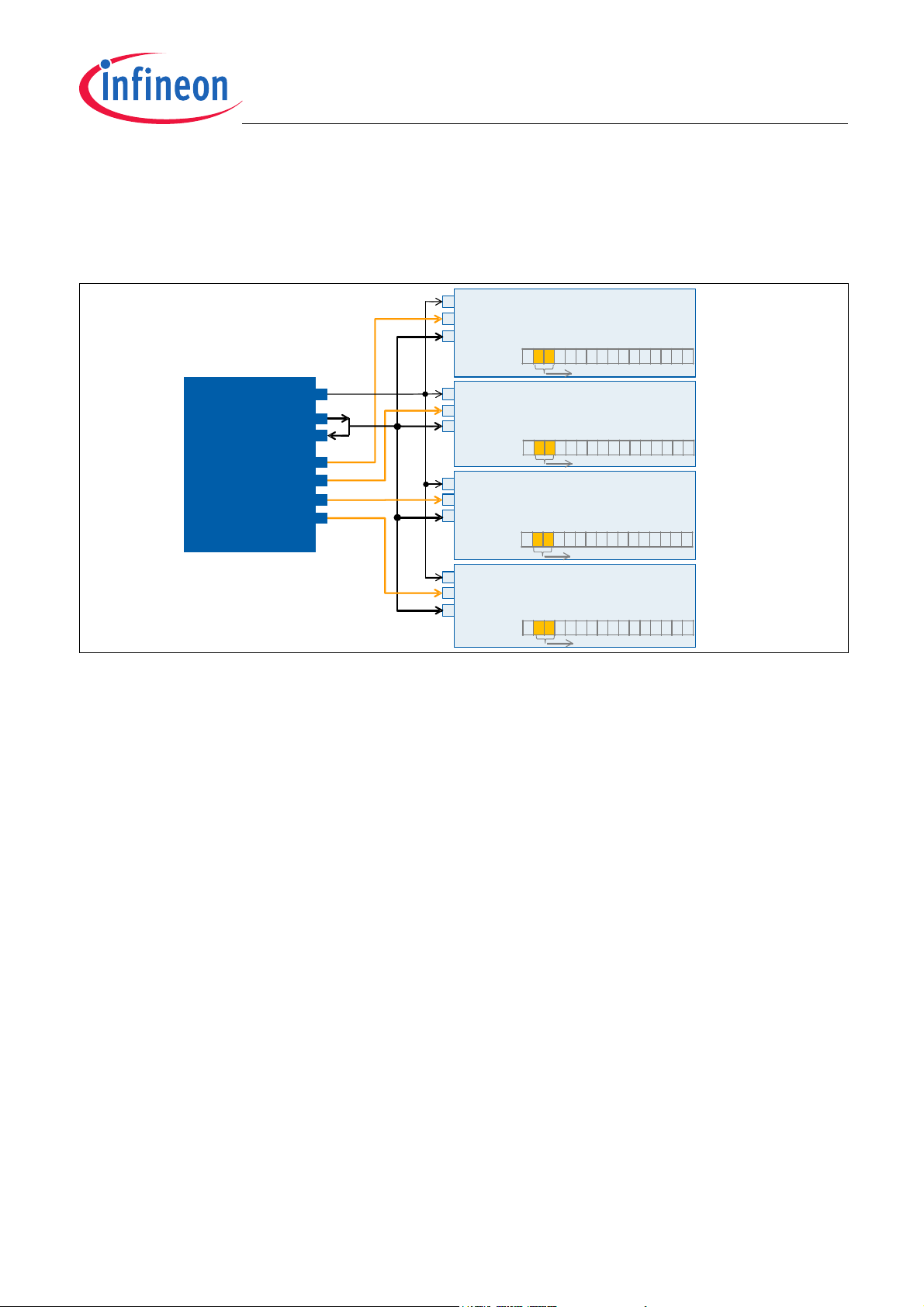
TLE5012B
SPI
master
(µC)
SCK
SDI
CSQ
0
CSQ
1
CSQ
2
CSQ
3
SPI
slave 1
(TLE5012B)
SCK (pin #2)
CSQ (pin #3)
Data (pin #4)
SPI
slave 4
(TLE5012B)
SCK (pin #2)
CSQ (pin #3)
Data (pin #4)
SPI
slave 3
(TLE5012B)
SCK (pin #2)
CSQ (pin #3)
Data (pin #4)
SPI
slave 2
(TLE5012B)
SCK (pin #2)
CSQ (pin #3)
Data (pin #4)
x01xxxxxxxxxxxxx
x00xxxxxxxxxxxxx
x10xxxxxxxxxxxxx
x11xxxxxxxxxxxxx
STAT
(Status Register)
S_NR bits
STAT
(Status Register )
S_NR bits
STAT
(Status Register)
S_NR bits
STAT
(Status Register )
S_NR bits
SDO
Interfaces
5.2.3 TLE5012B in bus mode
Up to four slaves can be connected on the same bus (e.g. four TLE5012B, or two TLE5012B and two Linear Hall).
The master microcontroller (µC) will need four CSQ (chip select) pins to connect to each of the slaves (Daisy Chain
schemes are not possible).
Figure 5-6 Example of four slaves connected to a bus with one master with SSC interface
The TLE5012B particularity is that it is a 3-pin SSC (SPI) slave. One of these pins is for the Clock, another one is
for the Chip Select and the third one is for the Data (input and output). Since there is only one pin for the Data, the
output and input of the master have to be connected. When the sensor transmits data the master’s output pin
(SDO pin) has to be switched to high ohmic.
Clock generation
As described in Chapter 5.2.1 the master has to send a command word to start the communication between
master and slave. After that, the master has to trigger a clock so the slave can respond with the data and/or safety
word. To generate a clock set the direction of the master’s SDO pin to input and next write 0xFFFF in the SDO
register. A delay t
(see Table 5-2) has to be implemented before generating the clock for the answer.
wr_delay
With this a pulse of “1s” is generated and the clock triggered. Since the SDO has been set as an input pin, this
pulse of “1s” will not be transmitted and will not interefere with the data coming from the slave (sensor). This step
(writing 0xFFFF) has to be repeated as many times as reads from the slave are expected. This is usually twice;
one for the data and one for the safety word.
Slave Number configuration at start-up
With SSC the CSQ line ensures that the data sent -or received- goes to -or comes from- the correct slave. Still, if
the slave number (S_NR bits) are not configurated correctly at start-up, the safety word may report a wrong slave
number. The slave number may also be wrong in configurations with one single slave.
To ensure that the received slave number in the safety word is correct (RESP bits), configure the slave numbers
at start up with a write command. The slave number bits are described in the Status Register.
For configurations with only one or two slaves, it is also possible to configure the slave number at start up with the
SCK and IFC pins as done for the SPC interface (see Figure 5-12). The particularity with SSC interface is that the
SCK is a line connected to the master and therefore can only have on status at start-up. Setting the IFC pin at
“high” or “low” two slave numbers can be configurated.
User’s Manual 36 Rev. 1.2, 2018-02

TLE5012B
xor
X7 X6 X5 X4 X3 X2
xor
X0
xor
xor
Input
Serial
CRC
output
&
TX_CRC
1111 1 1 1
1
X1
parallel
Remainder
1
2348
++++ xxxx
100011101
Interfaces
5.2.4 Cyclic Redundancy Check (CRC)
A Cyclic Redundancy Check (CRC) is sent in the last 8 bits of the safety word.
• This CRC is according to the J1850 Bus Specification.
• Every new transfer restarts the CRC generation.
• The Command Word and all Data Words (in any direction) will be taken into account to generate the CRC. The
non-CRC bits -the 8 upper bits- of the safety word).
• Generator polynomial: X8+X4+X3+X2+1, but for the CRC generation the fast-CRC generation circuit is used
(see Figure 5-7)
• The seed value of the fast CRC circuit is ’11111111
• The remainder is inverted before transmission.
Figure 5-7 Fast CRC polynomial division circuit
’.
B
CRC calculation example with SSC interface
In this example the CRC generation for a typical SSC data transfer is shown. In this case the feature Prediction
will be enabled, so the SSC data transfer consists of a command word and a write data word send by the master
(microcrontroller) followed by a safety word -which contains the CRC- send by the slave (TLE5012B).
The command word 5081
this data has to be written in the address 08
indicates that a write data word (MSB of the command word at “0”) will follow and that
H
(MOD_2 register). The four LSBs of the command Word indicate
H
how many 16-bit words will follow (“0001B” in this case).
The write word 0804
is sent to enable Prediction, one of the features available with the TLE5012B. The PREDICT
H
bit (bit 2 of the WRITE Data 1) will be set at “1”.
Note: Before sending a Write Data, it is necessary to receive a Read Data to ensure that the bits that will not be
configurated (changed) are not overwritten with a wrong value (e.g. read-modify-write operation).
After writing the new configuration parameters, the sensor will send a safety word FE89
indicating the status
H
(STAT), the sensor number (RESP, “1110” in this case since there is only one sensor named “00”) and the CRC
(STAT and RESP are not included in its generation). In this case the CRC transmitted is 89
.
H
CRC generation
At the beginning the CRC is set at 00
(see Figure 5-9, line 1). The first step to generate the CRC consists in a
H
XOR logical operation (line 3) between the 8 MSB bits of the Command Word (line 1) and the seed value 1111111
(line 2). Align the generator polynominal (line 4) to the non-zero MSB of the dataset out of the first step (line 3) and
calculate another XOR (line 5).
B
Figure 5-8 TLE5012B’s CRC generator polynomial for the SSC interface
From this point onwards reiterative XOR logical operations between the data (result of the previous operation) and
the generator polynominal are done till the remaining bits is equal or smaller than 00FF
User’s Manual 37 Rev. 1.2, 2018-02
(only 8 bits left). The
H

TLE5012B
W P
MSBLSBMSBLSBMSBLSB
1
01010000100000010000100000000100000000001111111010001001
2 Seed
11111111
3 XO R
10101111
4 Generator poly nomial
100011101
5 XO R
001000010
6 Generator poly nomial
100011101
7 XO R
000010101
8 Generator poly nomial
100011101
9 XO R
001001101
10 Generator poly nomial
100011101
11 XO R
000101011
12 Generator poly nomial
100011101
13 XO R
001000101
14 Generator poly nomial
100011101
15 XO R
000001011
16 Generator poly nomial
100011101
17 XO R
001111101
18 Generator poly nomial
100011101
19 XO R
011101001
20 Generator poly nomial
100011101
21 XO R
011001110
22 Generator poly nomial
100011101
23 XO R
010000001
24 Generator poly nomial
100011101
25 XO R
000011111
26 Generator poly nomial
100011101
27 XO R
011101101
28 Generator poly nomial
100011101
29 XO R
011000111
30 Generator poly nomial
100011101
31 XO R
010010011
32 Generator poly nomial
100011101
33 XO R
0001110110
34 In verted Rema ind er
10001001
35
COMMAND W RITE Data 1 SAFETY-WORD
LOCK ADDR ND A NG_RANGE S TAT RESP CRC
89
CRC
CALCULATION
5081
H
0804
H
FE00H -> FE89
H
Interfaces
genarator polynomial always has to be aligned to the non-zero MSB of the dataset. Finally the CRC value (line 33)
has to be inverted (XOR with a all “1”s polynominal) to generate the Inverted Remainder (line 34).
Figure 5-9 CRC generation example with SSC interface
User’s Manual 38 Rev. 1.2, 2018-02
H

TLE5012B
CRC generation software code example
Two software codes with C-language to generate CRC are provided. The first example is a more intuitive though
slower solution, since two iterative loops are done; a loop for each byte and an inner loop for each bit. It is also a
compact solution.
The second code is faster, since the inner loop is implemented as a look-up table (LUT). Therefore, the CRC does
not need to be calculated each time, but is taken from the look-up table, saving some computational time. As a
look-up table is required, some extra memory space is needed compared to the first example.
Example 1:
//“message” is the data transfer for which a CRC has to be calculated.
//A typical “message” consists of 2 bytes for the command word plus 2 bytes for the
//data word plus 2 bytes for the safety word.
//“Bytelength” is the number of bytes in the “message”. A typical “message” has 6
//bytes.
unsigned char CRC8(unsigned char *message, unsigned char Bytelength)
{
//“crc” defined as the 8-bits that will be generated through the message till the
//final crc is generated. In the example above this are the blue lines out of the
//XOR operation.
unsigned char crc;
Interfaces
//“Byteidx” is a counter to compare the bytes used for the CRC calculation
unsigned char Byteidx, Bitidx;
//Initially the CRC remainder has to be set with the original seed (0xFF for the
//TLE5012B).
crc = 0xFF;
//For all the bytes of the message.
for(Byteidx=0; Byteidx<Bytelength; Byteidx++)
{
//“crc” is calculated as the XOR operation from the previous “crc” and the “message”.
//“^” is the XOR operator.
crc ^= message[Byteidx];
//For each bit position in a 8-bit word
for(Bitidx=0; Bitidx<8; Bitidx++)
{
//If the MSB of the “crc” is 1(with the &0x80 mask we get the MSB of the crc).
if((crc&0x80)!=0)
{
//“crc” advances on position (“crc” is moved left 1 bit: the MSB is deleted since it
//will be cancelled out with the first one of the generator polynomial and a new bit
//from the “message” is taken as LSB.)
crc <<=1;
//“crc” is calculated as the XOR operation from the previous “crc” and the generator
//polynomial (0x1D for TLE5012B). Be aware that here the x8 bit is not taken since
//the MSB of the “crc” already has been deleted in the previous step.
crc ^= 0x1D;
}
User’s Manual 39 Rev. 1.2, 2018-02

TLE5012B
//In case the crc MSB is 0.
else
//“crc” advances one position (this step is to ensure that the XOR operation is only
//done when the generator polynomial is aligned with a MSB of the message that is “1”.
crc <<= 1;
}
}
//Return the inverted “crc” remainder(“~” is the invertion operator). An alternative
//to the “~” operator would be a XOR operation between “crc” and a 0xFF polynomial.
return(~crc);
}
Example 2:
The function that generates the CRC:
//“message” is the data transfer for which a CRC has to be calculated.
//A typical “message” consists of 2 bytes for the command word plus 2 bytes for the
//data word plus 2 bytes for the safety word.
//“Bytelength” is the number of bytes in the “message”. A typical “message” has 6
//bytes.
//*Table CRC is the pointer to the look-up table (LUT)
unsigned char CRC8(unsigned char *message, unsigned char Bytelength, unsigned char
* TableCRC)
{
Interfaces
//“crc” defined as the 8-bits that will be generated through the message till the
//final crc is generated. In the example above this are the blue lines out of the
//XOR operation.
unsigned char crc;
//“Byteidx” is a counter to compare the bytes used for the CRC calculation and
//“Bytelength”.
unsigned char Byteid;
//Initially the CRC remainder has to be set with the original seed (0xFF for the
//TLE5012B).
crc = 0xFF;
//For all the bytes of the message.
for(Byteidx=0; Byteidx<Bytelength; Byteidx++)
{
//“crc” is the value in the look-up table TableCRC[x] at the position “x”.
//The position “x” is determined as the XOR operation between the previous “crc” and
//the next byte of the “message”.
//“^” is the XOR operator.
crc = TableCRC[crc ^ *(message+Byteidx)];
}
//Return the inverted “crc” remainder(“~” is the invertion operator). An alternative
//to the “~” operator would be a XOR operation between “crc” and a 0xFF polynomial.
User’s Manual 40 Rev. 1.2, 2018-02

TLE5012B
return(~crc);
}
The look-up table -which depends on the CRC generator polynomial- required for the TLE5012B is as follows:
//Look-up table (LUT) for the TLE5012B with generator polynomial 100011101 (0x11D).
//As this table will be checked byte by byte, each byte has 256 possible values (2^8)
//for its CRC calculation with the given generator polynomial.
unsigned char TableCRC[256]
{
//The “crc” of the position [1] (result from operation [crc ^*(message+Byteidx)])
//is 0x00 -> 0x00 XOR 0x11D = 0x00 (1 byte).
0x00,
//The “crc” of the position [2] is 0x1D -> 0x01 XOR 0x11D = 0x1D (1 byte).
0x1D,
//The “crc” of the position [3] is 0x3A -> 0x02 XOR 0x11D = 0x3A (1 byte).
0x3A,
//For all the rest of the cases.
0x27, 0x74, 0x69, 0x4E, 0x53, 0xE8, 0xF5, 0xD2, 0xCF, 0x9C, 0x81, 0xA6, 0xBB, 0xCD,
0xD0, 0xF7, 0xEA, 0xB9, 0xA4, 0x83, 0x9E, 0x25, 0x38, 0x1F, 0x02, 0x51, 0x4C, 0x6B,
0x76, 0x87, 0x9A, 0xBD, 0xA0, 0xF3, 0xEE, 0xC9, 0xD4, 0x6F, 0x72, 0x55, 0x48, 0x1B,
0x06, 0x21, 0x3C, 0x4A, 0x57, 0x70, 0x6D, 0x3E, 0x23, 0x04, 0x19, 0xA2, 0xBF, 0x98,
0x85, 0xD6, 0xCB, 0xEC, 0xF1, 0x13, 0x0E, 0x29, 0x34, 0x67, 0x7A, 0x5D, 0x40, 0xFB,
0xE6, 0xC1, 0xDC, 0x8F, 0x92, 0xB5, 0xA8, 0xDE, 0xC3, 0xE4, 0xF9, 0xAA, 0xB7, 0x90,
0x8D, 0x36, 0x2B, 0x0C, 0x11, 0x42, 0x5F, 0x78, 0x65, 0x94, 0x89, 0xAE, 0xB3, 0xE0,
0xFD, 0xDA, 0xC7, 0x7C, 0x61, 0x46, 0x5B, 0x08, 0x15, 0x32, 0x2F, 0x59, 0x44, 0x63,
0x7E, 0x2D, 0x30, 0x17, 0x0A, 0xB1, 0xAC, 0x8B, 0x96, 0xC5, 0xD8, 0xFF, 0xE2, 0x26,
0x3B, 0x1C, 0x01, 0x52, 0x4F, 0x68, 0x75, 0xCE, 0xD3, 0xF4, 0xE9, 0xBA, 0xA7, 0x80,
0x9D, 0xEB, 0xF6, 0xD1, 0xCC, 0x9F, 0x82, 0xA5, 0xB8, 0x03, 0x1E, 0x39, 0x24, 0x77,
0x6A, 0x4D, 0x50, 0xA1, 0xBC, 0x9B, 0x86, 0xD5, 0xC8, 0xEF, 0xF2, 0x49, 0x54, 0x73,
0x6E, 0x3D, 0x20, 0x07, 0x1A, 0x6C, 0x71, 0x56, 0x4B, 0x18, 0x05, 0x22, 0x3F, 0x84,
0x99, 0xBE, 0xA3, 0xF0, 0xED, 0xCA, 0xD7, 0x35, 0x28, 0x0F, 0x12, 0x41, 0x5C, 0x7B,
0x66, 0xDD, 0xC0, 0xE7, 0xFA, 0xA9, 0xB4, 0x93, 0x8E, 0xF8, 0xE5, 0xC2, 0xDF, 0x8C,
0x91, 0xB6, 0xAB, 0x10, 0x0D, 0x2A, 0x37, 0x64, 0x79, 0x5E, 0x43, 0xB2, 0xAF, 0x88,
0x95, 0xC6, 0xDB, 0xFC, 0xE1, 0x5A, 0x47, 0x60, 0x7D, 0x2E, 0x33, 0x14, 0x09, 0x7F,
0x62, 0x45, 0x58, 0x0B, 0x16, 0x31, 0x2C, 0x97, 0x8A, 0xAD, 0xB0, 0xE3, 0xFe,
//The “crc” of the position [255] is 0xD9 -> 0xFE XOR 0x11D = 0xD9 (1 byte).
0xD9,
//The “crc” of the position [256] is 0xC4 -> 0xFF XOR 0x11D = 0xC4 (1 byte).
0xC4
}
Interfaces
The following code does not need to be implemented since the look-up table is already provided above. But for
general interest the following code would be used to generate the look-up table independently of which generator
polynomial is used. This code can also be used to ensure that the values in the look-up table are correctly
generated/copied to the application.
//Generation of a look-up table (LUT)
void BuildCRCTable(unsigned int polynomial, unsigned char * crcTable)
{
//“ReducedPoly” is the generator polynomial
User’s Manual 41 Rev. 1.2, 2018-02

TLE5012B
unsigned char ReducedPoly;
unsigned int message;
unsigned char crc;
unsigned bitindex;
//Only 8 bits are taken
ReducedPoly = (unsigned char)(polynomial&0x00FF);
//For all the possible “message” combinations
for (message=0; message <= 0xFF; message++)
{
crc=(unsigned char)message;
//For all the bits of the byte.
for(Bitindex=0; Bitindex<8; Bitindex++)
{
//Calculation of the CRC
if((crc&0x80)!=0)
{
crc <<= 1;
crc ^= ReducedPoly;
}
else
crc <<=1;
}
//The value out of the CRC calculation for a certain “message” is saved in the
//position of the “message”.
*(crcTable+message) = crc;
}
}
Interfaces
Disclaimer
The CRC generation software code provided above shall be used as guidance to the developer of solutions with
the TLE5012B. Infineon is not responsible for malfunctioning of the code provided above. This code was used with
an Infineon's microcontroller XC878.
• The CRC generation software code is only provided as a hint for the implementation or the use of the Infineon
Technologies components and shall not be regarded as any description or warrant of a certain functionalities,
conditions or quality of the Infineon Technologies component(s).
• All statements contained in this code, including recommendation or suggestion or methodology, are to be
verified by the user before implementation or use, as operating conditions and environmental factors may
differ. The recipient of this code must verify any function described herein in the real application.
• Infineon Technologies hereby disclaims any and all warranties and liabilities of any kint (including without
limitation warranties of non-infringement of intellectual property rights of any third party) with respect to any
and all code given in this document.
User’s Manual 42 Rev. 1.2, 2018-02

TLE5012B
(
()
43925_*___
43925_*___
−−+=
−−+
OTRAWTTYTCOOFFSETYO
OTRAWTTXTCOOFFSETXO
Y
X
Interfaces
5.2.5 Angle Calculation with X-raw and Y-raw values
The TLE5012B’s COordinate Rotation DIgital Computer (CORDIC) contains the trigonometric function for angle
calculation. The angle value can be accessed reading the ANG_VAL register.
For safety checks and other purposes, it is also possible to calculate the angle value in a microcontroller by reading
the X-raw and Y-raw values from the TLE5012B. The raw values have to be compensated by either calculating
the offset, amplitude and phase parameters or by reading the registers which contain the pre-calibrated values.
The second case is recommended in cases where either the application does not turn full rotations (to calculate
the compensation parameters the whole sine and cosine signals are required) or it rotates at high speeds (enough
data has to be read to ensure that the maximum and minimum values of the sine and cosine are read).
5.2.5.1 Angle Calculation using pre-calibrated compensation values
For the angle calculation using pre-calibrated compensation values the following values have to be read from the
registers:
• X-raw value (ADC_X register, address 10
• Y-raw value (ADC_Y register, address 11
• T-raw value (T_RAW register, address 15
• T25O value (T25O register, address 30
• TCO_X_T value (MOD_4 register, address 0E
• TCO_Y_T value (TCO_Y register, address 0F
• X_OFFSET value (Offset X register, address 0A
• Y_OFFSET value (Offset Y register, address 0B
• SYNCH value (SYNCH register, address 0C
• ORTHO value (IFAB register, address 0D
• ANG_BASE value (MOD_3 register, address 09
The values T25O, TCO_X_T, TCO_Y_T, X_OFFSET, Y_OFFSET, SYNCH, ORTHO and ANG_BASE are values
specific for each device and constant (if autocalibration disabled). Therefore these values are required to be read
only once and saved to the microcontroller for re-use.
Refer to Chapter 6.2 for the description of the listed registers. These values have to be read with autocalibration
disabled.
)
H
)
H
)
H
)
H
)
H
)
H
)
H
)
H
)
H
)
H
)
H
X-raw and Y-raw values compensation
To increase the accuracy, the temperature-dependent offset drift can be compensated. The offset values O
O
can be described by Equation (5.1):
Y
=
)
and
X
(5.1)
T25O is a 7 bit register that has to be subtracted from the 10 bit T_RAW register. No shifts are required in this
operation, since the higher order bits of the T_RAW register are used to represent a wider range of values and not
a different resolution.
TCO_X_T and TCO_Y_T have 7 bits only and are multiplied with a 10 bit value. Therefore the result of the
multiplication has to be limited to the 10 MSBs (arithmetic shift by 7, if supported by compiler/architecture or signed
division by 128). In the last step of Equation (5.1), the 10 bit value for the temperature-dependent offset has to be
added to the 12 bit X_OFFSET and Y_OFFSET.
User’s Manual 43 Rev. 1.2, 2018-02

TLE5012B
Y
X
ORAWYY
ORAWXX
−=−=_
_
1
1
SYNCHYY
XX
*
12
12
=
=
)cos(
)sin(*
22
3
23
ORTHO
ORTHOXY
Y
XX
−
−−
=
BASEANG
X
Y
_arctan
3
3
−
⎟
⎟
⎠
⎞
⎜
⎜
⎝
⎛
=
α
Interfaces
After the X and Y values are read out, the temperature-corrected offset value must be subtracted:
(5.2)
X_RAW and Y_RAW are 16 bit values at which a 12 bit value is subtracted. Offsets are in the 12 bit range since
the values are smaller than the whole X_RAW and Y_RAW range.
Next, the Y value is normalized with the amplitude synchronicity:
(5.3)
While Y
is a 16 bit absolute value, SYNCH is a 12 bit relative factor (amplitude synchronicity is a relative correction
1
between the amplitude of the X-raw and Y-raw values). To convert SYNCH to absolute factor a normalized one
has to be added, this corresponds to add a value of 16,384 (2^14). After the multiplication Y
(16 bit from Y
and 14 bit from the SYNCH absolute factor which includes the added one), therefore it has to be
1
will be a 28 bit value
2
shifted to have the 16 MSBs only (arithmetic shift by 14, if supported by compiler/architecture or signed division
by 16384).
The influence of the non-orthogonality can be compensated using the following equation, in which only the Y value
must be corrected:
=
(5.4)
As described in the IFAB register (address 0D
11.2445° with a 12 bit resolution. Y
should finally be limited to 16 bits.
3
Angle calculation
After correction of all errors, the resulting angle can be calculated using the arctan function and subtracting the
angle base as shown in Equation (5.5):
To correctly resolve the arctan function in 360°, the microcontroller should implement the function arctan2(Y
ANG_BASE is a 12 bit register.
Small deltas from the ANG_VAL register may depend on the speed of application.
Figure 5-10 shows the flow chart of angle calculation from the X-raw and Y-raw values as described above.
), the ORTHO bits represent a value between -11.2500° and
H
(5.5)
3/X3
).
User’s Manual 44 Rev. 1.2, 2018-02

TLE5012B
Angle
Calculation
Non-Orthogonal ity
Correction
Amplitude
Normalization
Temperature-dependent
Offset Calculat ion
Offset
Compensation
readT_RAW
10bits
readT25O
7bits
T_RAW
10bits
‐
T25O
7bits
‐ 439
readTCO_X_T
7bits
readTCO_Y_T
7bits
readX_OFFSET
12bits
‐
Ox
12bits
+
x
readY_OFFSET
12bits
Oy
12bits
+
x
readSYNCH
12bits
x
Y1
16bits
readADC_X
16bits
readADC_Y
16bits
+
X1
16bits
+
Y2
16bits
X2
16bits
readORTHO
12bits
sin(‐ORTHO)
cos(‐ORTHO)
‐
/
x
Y3
16bits
X3
16bits
readANG_BASE
12bits
α
atan(Y3/X3)
‐
SYNCH
14bits
>>7
>>7
+2^14
>>14
Interfaces
Figure 5-10 Flow-Chart of Angle Calculation from the X-raw and Y-raw values
5.2.5.2 Angle Calculation with end-of-line calibration values
The TLE5012B already has pre-calibrated compensation parameters which can be used to calculate the angle
value (see Chapter 5.2.5.1). Own compensation parameters can also be calculated end-of-line if desired. In that
case check the Application Note TLE5009 Calibration.
User’s Manual 45 Rev. 1.2, 2018-02

TLE5012B
PWM
PWM
offonPWM
PWM
on
t
f
ttt
t
t
CycleDuty
1
=
+=
=
t
ON
‚0'
t
ON = High level OFF = Low level
Duty cycle = 6.25%
Duty cycle = 50%
Duty cycle = 93.75%
t
PWM
t
OFF
Vdd
U
IFA
Vdd
U
IFA
t
‚0'
t
Vdd
U
IFA
‚0'
Interfaces
5.3 Pulse Width Modulation Interface
The Pulse Width Modulation (PWM) interface can be selected via SSC (IF_MD = ‘01’) in the register MOD_4.
The PWM update rate can be programmed within the register 0E
resolution (including diagnostics):
• ~0.25 kHz
• ~0.5 kHz
• ~1.0 kHz
• ~2.0 kHz
PWM uses a square wave with constant frequency whose duty cycle is modulated according to the last measured
angle value (AVAL register).
Figure 5-11 shows the principal behavior of a PWM with various duty cycles and the definition of timing values.
The duty cycle of a PWM is defined by the following general formulas:
(IFAB_RES) in four possible steps with 12-bit
H
(5.6)
The duty cycle range between 0 - 6.25% and 93.75 - 100% is used only for diagnostic purposes. In case the sensor
detects an error, the corresponding error information will be transmitted by the PWM duty cycle, either in the lower
(0 - 6.25%) or upper (93.75 - 100%) diagnostic range, depending on the kind of error (see “Output duty cycle
range” in Table 5-7). As long as a fault is present, the error information will be transmitted in PWM frames. This
diagnostic function can be disabled via the MOD_4 register (see Chapter 6.2).
Sensors with preset PWM are available as TLE5012B E5xxx. The register settings for these sensors can be found
in Chapter 6.2.
Figure 5-11 Typical example of a PWM signal
User’s Manual 46 Rev. 1.2, 2018-02

TLE5012B
2*
IFAB_R ES
DIG
PWM
f
f =
PWM
PWM
ON
f
f
tAngle
1
*%5.87
360
*
1
*%25.6][
°
⎟
⎟
⎠
⎞
⎜
⎜
⎝
⎛
−=°
Interfaces
Table 5-7 PWM interface
Parameter Symbol Values Unit Note / Test Condition
Min. Typ. Max.
PWM output frequencies
(Selectable by IFAB_RES)
f
PWM1
f
PWM2
f
PWM3
f
PWM4
Output duty cycle range DY
PWM
232 244 262 Hz
464 488 525 Hz
929 977 1050 Hz
1855 1953 2099 Hz
6.25 93.75 % Absolute angle
1)
1)
1)
1)
1)
2 % Electrical Error (S_RST;
1)2)
S_VR)
98 % System error (S_FUSE;
S_OV; S_XYOL;
S_MAGOL; S_ADCT)
0 1 % Short to GND
1)
1)
99 100 % Short to VDD, power loss
1) Not subject to production test - verified by design/characterization
2) Both hardware and software resets will generate an Electrical Error duty cycle for the first PWM pulse after the reset
(S_RST). After readout, S_RST bit will be set to “0”, so the second PWM pulse will indicate an angle.
1)
The PWM frequency is derived from the digital clock via
(5.7)
4096*24
The min/max values given in Table 5-7 take into account the internal digital clock variation specified in TLE5012B
Data Sheet. If external clock is used, the variation of the PWM frequency can be derived from the variation of the
external clock using Equation (5.7).
Pulse length convertion to angle value
The length of the duty cycle represents the angle value. Whatever the absolute angle value is, the t
on the angle value calculated by the TLE5012B with resolution up to 0.100°. The 0.100° resolution is due to the
fact that with 12bit resolution (4096 steps) 100% of the duty cycle can be mapped, but only 87.5% of the duty cycle
translates to angle values. This means that the 360° degees must be mapped with only 3584 steps (87.5%*4096),
so effective resolution is 0.100°.
The angle value can be measured with the following formula, where t
f
is the frequency selected:
PWM
is the length of the pulse in seconds and
ON
time depends
on
(5.8)
The frequency for the PWM interface can be selected via the register MOD_4 (IFAB_RES bits) as described in
Chapter 6.2.1. See Chapter 7 for the PWM derivates with the default frequencies.
A t
of more than 93.75% duty cycle would indicate an error as described in Table 5-7.
ON
User’s Manual 47 Rev. 1.2, 2018-02

TLE5012B
SPC
master
(µC)
Data
SPC
slave 1
(TLE5012B)
IFC (pin #1)
SCK (pin #2)
IFA/SPC (pin #5)
SPC
slave 4
(TLE5012B)
IFC (pin #1)
SCK (pin #2)
IFA/SPC (pin #5)
SPC
slave 3
(TLE5012B)
IFC (pin #1)
SCK (pin #2)
IFA/SPC (pin #5)
SPC
slave 2
(TLE5012B)
IFC (pin #1)
SCK (pin #2)
IFA/SPC (pin #5)
x01xxxxxxxxxxxxx
x00xxxxxxxxxxxxx
x10xxxxxxxxxxxxx
x11xxxxxxxxxxxxx
STAT
(Status Register )
S_NR bits
STAT
(Status Regi ster)
S_NR bits
STAT
(Status Regi ster )
S_NR bits
STAT
(Status Register)
S_NR bits
GND
GND
GND
V
DD
V
DD
V
DD
GND
V
DD
The low time length of the
Trigger Nibble from the
master defines the specific
slave number
Interfaces
5.4 Short PWM Code (SPC)
The Short PWM Code (SPC) is a synchronized data transmission based on the SENT protocol (Single Edge
Nibble Transmission) defined by SAE J2716. As opposed to SENT, which implies a continuous transmission of
data, the SPC protocoll transmits data only after receiving a specific trigger pulse from the microcontroller. The
required length of the trigger pulse depends on the sensor number, which is configurable. Thereby, SPC allows
the operation of up to four sensors on one bus line.
SPC enables the use of enhanced protocol functionality due to the ability to select between various sensor slaves
(ID selection). The slave number (S_NR) can be given by the external circuit of SCK and IFC pin. In case of V
on SCK, the S_NR[0] can be set to 1 and in the case of GND on SCK the S_NR[0] is equal to 0. S_NR[1] can be
adjusted in the same way by the IFC pin. Only one data line to the slaves is necessary, as the length of the trigger
nibble will awake one or the other slaves, as explained in the next paragraph.
DD
Figure 5-12 Example of four slaves connected to a bus with one master with SPC interface
As in SENT, the time between two consecutive falling edges defines the value of a 4-bit nibble, thus representing
numbers between 0 and 15. The transmission time therefore depends on the transmitted data values. The single
edge is defined by a 3 Unit Time (UT, see Chapter 5.4.1) low pulse on the output, followed by the high time defined
in the protocol (nominal values, may vary depending on the tolerance of the internal oscillator and the influence of
external circuitry). All values are multiples of a unit time frame concept. A transfer consists of the following parts
(Figure 5-13):
• A trigger pulse by the master, which initiates the data transmission
• A synchronization period of 56 UT (in parallel, a new sample is calculated)
• A status nibble of 12-27 UT
• Between 3 and 6 data nibbles of 12-27 UT
• A CRC nibble of 12-27 UT
• An end pulse to terminate the SPC transmission
User’s Manual 48 Rev. 1.2, 2018-02

TLE5012B
Sync hr onisati on Fram e Status -Nibbl e
Dat a - Ni bble 1
Bit 11 -8
Dat a -Ni bbl e 2
Bit 7 -4
Dat a - Nibbl e 3
Bit 3- 0
CRC
56 tck 12..27 tck 12 .. 27 tck 12.. 27 tck 12 ..27 tc k 12..27 tck
Ni bble-Encodi ng : ( 12+x) *tck
Ti m e-Base : 1 tck (3µ s+ /-dtck )
Tr igger N ibble End -Pulse
24,34 ,51,78 tck 12 tck
µC Activ ity
Sensor Acti vi ty
Sync hr onis ation Fr ame
...
Tr igger N ibble End - Pulse
µC Activity
Sensor Acti vi ty
Sync hronis ation Fr ame
...
Tr igger Ni bble
> 90 µs
End- Pulse
SPI
master
(µC)
Data
SPI
slave x
(TLE5012B)
IFC (pin #1)
SCK (pin #2)
IFA/SPC
(pin #5)
V
DD
1kΩ
Interfaces
Figure 5-13 SPC frame example
The CRC checksum includes the status nibble and the data nibbles. It can be used to check the validity of the
decoded data. The sensor is available for the next trigger pulse 90μs after the falling edge of the end pulse (see
Figure 5-14).
Figure 5-14 SPC pause timing diagram
In SPC mode, the sensor does not continuously calculate an angle from the raw data. Instead, the angle
calculation starts after the recognized trigger nibble from the master in order to minimize timing jitter. In this mode,
the AVAL register, which stores the angle value and can be read via SSC, contains the angle which was calculated
after the last SPC trigger nibble.This means that in any case, to update the registers and read the data via SSC,
a trigger nibble has to be previously generated.
Figure 5-15 SPC configuration in open drain mode
In parallel to SPC, the SSC interface can be used for individual configuration. The number of transmitted SPC
nibbles can be changed to customize the amount of information sent by the sensor. The frame contains a 16-bit
angle value and an 8-bit temperature value in the full configuration (Table 5-8).
Sensors with preset SPC are available as TLE5012B E9000. The register settings for these sensors can be found
in the Chapter 7.
User’s Manual 49 Rev. 1.2, 2018-02

TLE5012B
Interfaces
Table 5-8 Frame configuration
Frame type IFAB_RES Data nibbles
12-bit angle 00 3 nibbles
16-bit angle 01 4 nibbles
12-bit angle, 8-bit temperature 10 5 nibbles
16-bit angle, 8-bit temperature 11 6 nibbles
The status nibble, which is sent with each SPC data frame, provides an error indication similar to the Safety Word
of the SSC protocol. In case the sensor detects an error, the corresponding error bit in the Status register is set
and either the bit SYS_ERR or the bit ELEC_ERR of the status nibble will be “high”, depending on the kind of error
(see Table 5-9). As long as a fault is present, the error information will be transmitted in SPC frames. Any fault will
be communicated at least once by the SPC frame (even if the fault happened and disappeared before the trigger
nibble).
Table 5-9 Structure of status nibble
Name Bits Description
SYS_ERR [3] Indication of system error (S_FUSE, S_OV, S_XYOL, S_MAGOL, S_ADCT)
0: No system error
1: System error occurred
ELEC_ERR [2] Indication of electrical error (S_RST, S_VR)
0: No electrical error
1: Electrical error occurred
Both hardware and software resets will set this bit at “1” for the first status
nibble after the reset (S_RST).
S_NR [1] Slave number bit 1 (level on IFC)
[0] Slave number bit 0 (level on SCK)
5.4.1 Unit Time Setup
The basic SPC protocol unit time granularity is defined as 3 μs. Every timing is a multiple of this basic time unit.To
achieve more flexibility, trimming of the unit time can be done within IFAB_HYST. This enables a setup of different
unit times.
Table 5-10 Predivider setting
Parameter Symbol Values Unit Note / Test Condition
Min. Typ. Max.
Unit time
t
Unit
3.0 μs IFAB_HYST = 00
2.5 IFAB_HYST = 01
2.0 IFAB_HYST = 10
1.5 IFAB_HYST = 11
1) Not subject to production test - verified by design/characterization
User’s Manual 50 Rev. 1.2, 2018-02
1)
1)
1)
1)

TLE5012B
SPC
ECU trigger
level
V
th
t
mlow
t
md,tot
t
mtr
Interfaces
5.4.2 Master Trigger Pulse Requirements
An SPC transmission is initiated by a master trigger pulse on the IFA pin. To detect a low-level on the IFA pin, the
voltage must be below a threshold V
crossed. Figure 5-16 shows the timing definitions for the master pulse. The master low time t
total trigger time t
are given in Table 5-11.
mtr
If the master low time exceeds the maximum low time, the sensor does not respond and is available for a next
triggering 30 μs after the master pulse crosses V
in the sensor and the triggering of the ECU.
. The sensor detects that the IFA line has been released as soon as Vth is
th
as well as the
mlow
. t
thr
is the delay between internal triggering of the falling edge
md,tot
Figure 5-16 SPC Master pulse timing
Table 5-11 Master pulse parameters
Parameter Symbol Values Unit Note / Test Condition
Min. Typ. Max.
Threshold
Threshold hysteresis V
Total trigger time t
V
th
thhyst
mtr
50 % of
V
DD
8% ofV
3V
DD
90 UT SPC_Trigger = 0;
t
mlow
UT SPC_Trigger = 1
1)
= 5 V
DD
VDD = 3 V
1)
1)
1)2)
1)
+12
Master low time t
mlow
8 12 14 UT S_NR =00
16 22 27 S_NR =01
29 39 48 S_NR =10
50 66 81 S_NR =11
Master delay time t
md,tot
5.8 μs
1) Not subject to production test - verified by design/characterization
2) Trigger time in the sensor is fixed to the number of units specified in the “typ.” column, but the effective trigger time varies
due to the sensor’s clock variation
1)
1)
1)
1)
1)
Total trigger time
The SPC_Trigger is set to 0 by default. For a variable-length SPC Trigger Nibble -and therefore an overall shorter
SPC Frame- the SPC_Trigger bit can be set to 1 via the SSC interface. The SPC_Trigger bit is the second MSB
of the HSM_PLP bits of the MOD_4 register (address 0E
). Check Chapter 6.2 for further details.
H
User’s Manual 51 Rev. 1.2, 2018-02

TLE5012B
1
234
+++ xxx
11101
MSBLSBMSBLSBMSBLSBMSBLSBMSBLSB
1
00000111100100110000
2 Seed
0101
3 XOR
0101
4 Generator polynomial
11101
5 XOR
01000
6 Generator polynomial
11101
7 XOR
01100
8 Generator polynomial
11101
9 XOR
00100
10 Generator polynomial
11101
11 XOR
01111
12 Generator polynomial
11101
13 XOR
00011
14 Generator polynomial
11101
15 XOR
00001
16 Generator polynomial
11101
17 XOR
00001
18 Remainder
0100
20
CRC
4
D
Status-Nibble Data-Nibble 1 Data-Nibble 2 Data-Nibble 3
Interfaces
5.4.3 Checksum Nibble Details
The checksum nibble is a 4-bit CRC of the data nibbles including the status nibble. The CRC is calculated using
the polynomial x
transferred as CRC.
CRC calculation example with SPC interface:
The following example shows the CRC generation for a typical SPC frame with three data nibbles (default setting).
The status nibble is 0000
ground as shown in the application circuits chapter). The following three data nibbles provide the angle value.
At the beginning the CRC is set at 0000
a XOR logical operation (line 3) between the status nibble (line 1) and the seed value 0101
generator polynomial (line 4) to the non-zero MSB of the dataset out of the first step (line 3) and calculate another
XOR (line 5).
Figure 5-17 TLE5012B’s CRC generator polynomial for the SPC interface
4+x3+x2
+1 with a seed value of 0101. The remainder after the last data nibble is used are
as there are no errors and the slave number is the 00B (IFC and SCK pin connected to
B
(see Figure 5-18, line 1). The first step to generate the CRC consists in
B
(line 2). Align the
B
From this point onwards, reiterative XOR logical operations between the data (result of the previous operation)
and the generator polynomial are done till the remaining bits are equal or smaller than 0x0F
Figure 5-18 CRC generation example with SPC interface
User’s Manual 52 Rev. 1.2, 2018-02
(only 4 bits left).
H

TLE5012B
CRC generation software code example
//“message” is the data transfer for which a CRC has to be calculated.
//A typical “message” consists of the status nibble, three data nibbles and the CRC
//nibble (the trigger nibble and the synchronisation nibble are not part of the CRC).
//“Length” is the number of nibbles in the “message”. A typical “message” has 5
//nibbles (the trigger nible and the synchronization nibble are not part of the CRC).
unsigned char CRC(unsigned char *message, unsigned char Length)
{
//“crc” defined as the 4-bits that will be generated through the message till the
//final “crc” is generated. In the example above this are the blue lines out of the
//XOR operation.
unsigned char crc;
//“Numnibbles” is a counter to compare the bits used for the CRC calculation and
//“Length”.
unsigned char Numnibbles, bitdata;
//Initially the CRC remainder has to be set with the original seed (0x05 for the
//TLE5012B).
crc = 0x05;
Interfaces
//For all the nibbles of the message.
for(Numnibbles=0; Numnibbles<Length; Numnibbles++)
{
//“crc” is calculated as the XOR operation from the previous “crc” and the “message”.
//“^” is the XOR operator.
crc ^= message[Numnibbles];
//For each bit position in a 4-bit nibble
for(bitdata=0; bitdata<4; bitdata++)
{
//If the MSB of the “crc” is 1 (with the &0x80 mask we get the MSB of the crc).
if((crc&0x08)!=0)
{
//“crc” advances on position (“crc” is moved left 1 bit: the MSB is deleted since it
//will be cancelled out with the first one of the generator polynomial and a new bit
//from the “message” is taken as LSB.)
crc <<=1;
//“crc” is calculated as the XOR operation from the previous “crc” and the generator
//polynomial (0x0D for TLE5012B). Be aware that here the x4 bit is not taken since
//the MSB of the “crc” already has been deleted in the previous step.
crc ^= 0x0D;
}
//In case the “crc” MSB is 0
else
//“crc” advances one position (this step is to ensure that the XOR operation is only
//done when the generator polynomial is aligned with a MSB of the message that is “1”.
crc <<= 1;
}
}
User’s Manual 53 Rev. 1.2, 2018-02

TLE5012B
//Return the “crc” remainder. The &0x0F mask is a safety check to ensure four LSBs
//only and rest 0’s.
return(crc&0x0F);
}
Disclaimer
The CRC generation software code provided above shall be used as guidance to the developer of solutions with
the TLE5012B. Infineon is not responsible for malfunctioning of the code provided above. This code was used with
an Infineon's microcontroller XC878.
• The CRC generation software code is only provided as a hint for the implementation or the use of the Infineon
Technologies components and shall not be regarded as any description or warrant of a certain functionalities,
conditions or quality of the Infineon Technologies component(s).
• All statements contained in this code, including recommendation or suggestion or methodology, are to be
verified by the user before implementation or use, as operating conditions and environmental factors may
differ. The recipient of this code must verify any function described herein in the real application.
• Infineon Technologies hereby disclaims any and all warranties and liabilities of any kint (including without
limitation warranties of non-infringement of intellectual property rights of any third party) with respect to any
and all code given in this document.
Interfaces
User’s Manual 54 Rev. 1.2, 2018-02

TLE5012B
HS1
HS2
HS3
0°Electrical Angle 60° 120° 180° 240° 300° 360°
Hall-Switch-Mode: 3phase Generation
Angle
Mech. Angle with
5 Pole Pairs
0° 12° 24° 36° 48° 60° 72°
0° 20° 40° 60° 80° 100° 120°
Mech. Angle with
3 Pole Pairs
Interfaces
5.5 Hall Switch Mode (HSM)
The Hall Switch Mode (HSM) within the TLE5012B makes it possible to emulate the output of 3 Hall switches. Hall
switches are often used in electrical commutated motors to determine the rotor position. With these 3 output
signals, the motor will be commutated in the right way. Depending on which pole pairs of the rotor are used, various
electrical periods have to be controlled. This is selectable within 0E
output signals with the relationship between electrical angle and mechanical angle. The mechanical 0° point is
always used as reference.
The HSM is generally used with push-pull output, but it can be changed to open-drain within the register IFAB_OD.
Sensors with preset HSM are available as TLE5012B E3xxx. The register settings for these sensors can be found
in the Chapter 6.2.
(HSM_PLP). Figure 5-19 depicts the three
H
Figure 5-19 Hall Switch Mode
The HSM Interface can be selected via SSC (IF_MD = 010).
Table 5-12 Hall Switch Mode
Parameter Symbol Values Unit Note / Test Condition
Rotation speed n 10000 rpm Mechanical
User’s Manual 55 Rev. 1.2, 2018-02
Min. Typ. Max.
2)

TLE5012B
Interfaces
Table 5-12 Hall Switch Mode (cont’d)
Parameter Symbol Values Unit Note / Test Condition
Min. Typ. Max.
Electrical angle accuracy
elect
0.6 1 ° 1 pole pair with
autocalibration
1)2)
1.2 2 ° 2 pole pairs with autocal.
1.8 3 ° 3 pole pairs with autocal.
2.4 4 ° 4 pole pairs with autocal.
3.0 5 ° 5 pole pairs with autocal.
3.6 6 ° 6 pole pairs with autocal.
4.2 7 ° 7 pole pairs with autocal.
4.8 8 ° 8 pole pairs with autocal.
5.4 9 ° 9 pole pairs with autocal.
6.0 10 ° 10 pole pairs with
autocal.
1)2)
6.6 11 ° 11 pole pairs with
autocal.
1)2)
7.2 12 ° 12 pole pairs with
autocal.
1)2)
7.8 13 ° 13 pole pairs with
autocal.
1)2)
8.4 14 ° 14 pole pairs with
autocal.
1)2)
9.0 15 ° 15 pole pairs with
autocal.
1)2)
9.6 16 ° 16 pole pairs with
1)2)
2)3)4)
Mechanical angle switching
hysteresis
HShystm
autocal.
0 0.703 ° Selectable by
IFAB_HYST
1)2)
1)2)
1)2)
1)2)
1)2)
1)2)
1)2)
1)2)
User’s Manual 56 Rev. 1.2, 2018-02

TLE5012B
Interfaces
Table 5-12 Hall Switch Mode (cont’d)
Parameter Symbol Values Unit Note / Test Condition
Min. Typ. Max.
Electrical angle switching
hysteresis
5)
HShystel
0.70 ° 1 pole pair;
IFAB_HYST=11
1)2)
1.41 ° 2 pole pairs;
IFAB_HYST=11
1)2)
2.11 ° 3 pole pairs;
IFAB_HYST=11
1)2)
2.81 ° 4 pole pairs;
IFAB_HYST=11
1)2)
3.52 ° 5 pole pairs;
IFAB_HYST=11
1)2)
4.22 ° 6 pole pairs;
IFAB_HYST=11
1)2)
4.92 ° 7 pole pairs;
IFAB_HYST=11
1)2)
5.62 ° 8 pole pairs;
IFAB_HYST=11
1)2)
6.33 ° 9 pole pairs;
IFAB_HYST=11
1)2)
7.03 ° 10 pole pairs;
IFAB_HYST=11
1)2)
7.73 ° 11 pole pairs;
IFAB_HYST=11
1)2)
8.44 ° 12 pole pairs;
IFAB_HYST=11
1)2)
9.14 ° 13 pole pairs;
IFAB_HYST=11
1)2)
9.84 ° 14 pole pairs;
IFAB_HYST=11
1)2)
10.55 ° 15 pole pairs;
IFAB_HYST=11
1)2)
11.25 ° 16 pole pairs;
1)2)
Fall time t
Rise time t
HSfall
HSrise
0.02 1 μsRL = 2.2k; CL < 50pF
0.4 1 μsRL = 2.2k; CL < 50pF
1) Depends on internal oscillator frequency variation (see Data Sheet)
2) Not subject to production test - verified by design/characterization
3) GMR hysteresis not considered
4) Minimum hysteresis without switching
5) The hysteresis has to be considered only at change of rotation direction
IFAB_HYST=11
2)
2)
To avoid switching due to mechanical vibrations of the rotor, an artificial hysteresis is recommended (Figure 5-20).
User’s Manual 57 Rev. 1.2, 2018-02
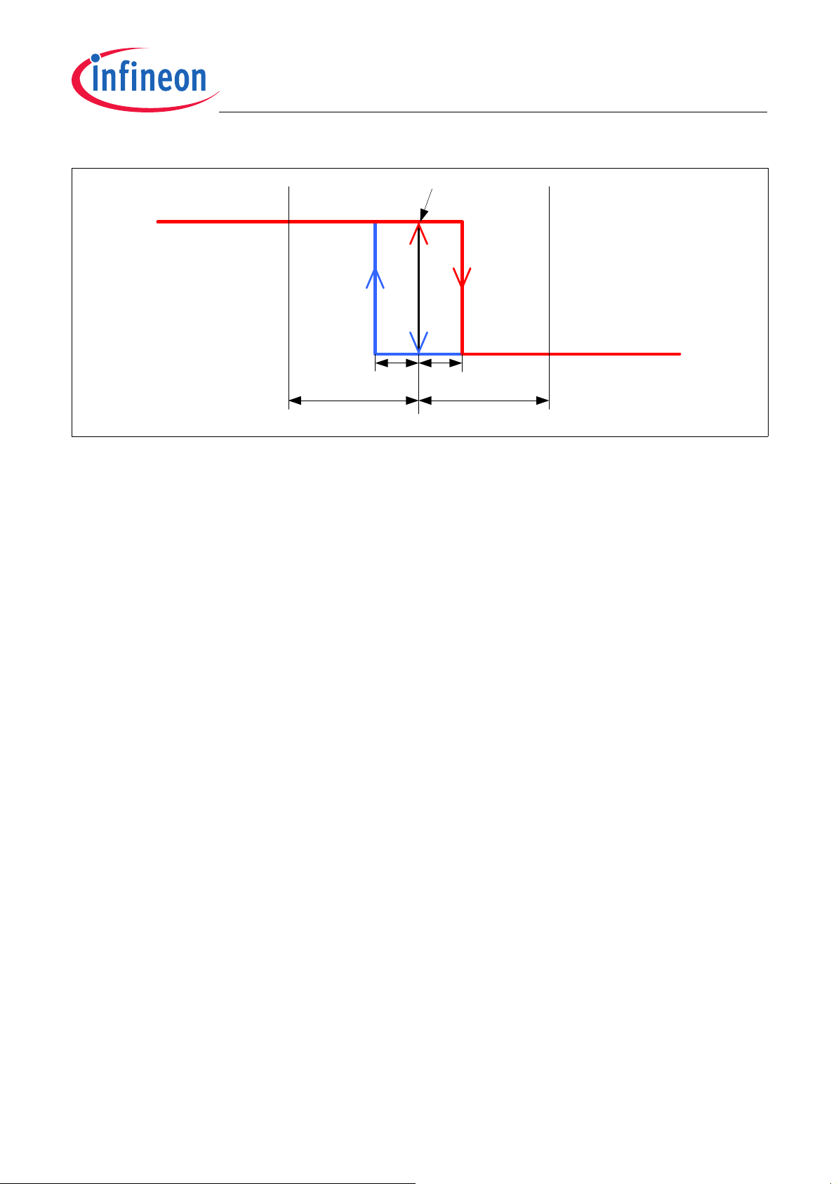
TLE5012B
Ideal Switching Point
elect
HShystel
HSh ystel
elect
0°
Figure 5-20 HS hysteresis
Interfaces
User’s Manual 58 Rev. 1.2, 2018-02
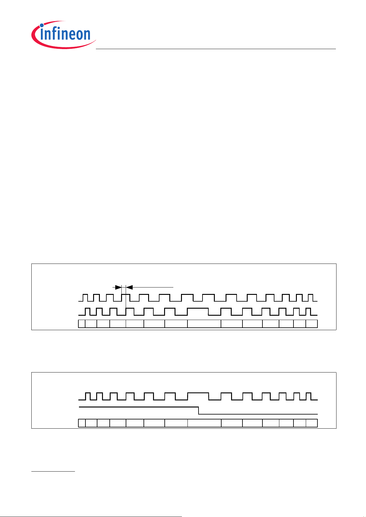
TLE5012B
90° el . Phase shi ft
0 1 2 3 4 5 6 7 6 5 4 3 2 1
Phase A
Counter
Phase B
Increment al Interf ace
(A/B Mode)
V
H
V
L
V
H
V
L
Step
Counter
Direction
Incremen t al Interf ace
(Step/Direction Mode)
V
H
V
L
V
H
V
L
0 1 2 3 4 5 6 7 6 5 4 3 2 1
Interfaces
5.6 Incremental Interface (IIF)
The Incremental Interface (IIF) emulates the operation of an optical quadrature encoder with a 50% duty cycle. It
transmits a square pulse per angle step, where the width of the steps can be configured from 9bit (512 steps per
full rotation) to 12bit (4096 steps per full rotation) within the register MOD_4 (IFAB_RES)
is given either by the phase shift between the two channels IFA and IFB (A/B mode) or by the level of the IFB
channel (Step/Direction mode), as shown in Figure 5-21 and Figure 5-22. The incremental interface can be
configured for A/B mode or Step/Direction mode in register MOD_1 (IIF_MOD).
Using the Incremental Interface requires an up/down counter on the microcontroller, which counts the pulses and
thus keeps track of the absolute position. The counter can be synchronized periodically by using the SSC interface
in parallel. The angle value (AVAL register) read out by the SSC interface can be compared to the stored counter
value. In case of a non-synchronization, the microcontroller adds the difference to the actual counter value to
synchronize the TLE5012B with the microcontroller.
After startup, the IIF transmits a number of pulses which correspond to the actual absolute angle value. Thus, the
microcontroller gets the information about the absolute position. The Index Signal that indicates the zero crossing
is available on the IFC pin.
Sensors with preset IIF are available as TLE5012B E1000. The register settings for these sensors can be found
in Chapter 6.2.
A/B Mode
1)
. The rotation direction
The phase shift between Phase A and Phase B is determined by the rotation direction of the magnet. By default
(ANG_DIR = 0), Phases A follows Phase B to indicate clockwise rotation direction, while Phase B follows Phase
A to indicate counterclockwise rotation direction. This behaviour is inverted by setting ANG_DIR = 1.
Figure 5-21 Incremental interface with A/B mode
Step/Direction Mode
Phase A pulses out the increments and phase B indicates the direction.
Figure 5-22 Incremental interface with Step/Direction mode
1) Decreasing the number of bits does not increase the maximum rotation speed.
User’s Manual 59 Rev. 1.2, 2018-02

TLE5012B
Angle Value is pulsed out at start-up
…
…
Phase B
Phase A
2 steps turned
3 steps turned
(at higher speed than
the previous 2 steps)
90
phase
B-A
90
phase
B-A
12
360*#
=
pulses
angle
612
360*(sec)
−
=
length
angle
Interfaces
Startup pulses
Just after startup, in absolute mode (default mode in the register MOD_4, bits HSM_PLP), the IIF generates the
number of pulses needed to count to the initial angle position on the shortest direction. These pulses may be
generated at the maximum frequency on both IFA and IFB pin (see Table 5-13) and therefore the start up pulses
may take up to 2.1ms to count to an initial angle position of 180° (maximum angular distance). The counting
direction may change once the startup position has been reached (depending on whether the shortest direction
matched the actual rotation direction or not).Changes of angle position from the initial position during the start-up
pulses are tracked.
Figure 5-23 Increcremental Interface startup pulses and first step movements at different speeds
The number of pulses indicates the angle value position. The angle can be calculated counting the numjber of
pulses:
(5.9)
°
2
Or measuring the length (in seconds) of the train of pulses:
(5.10)
°
10*2
The actual increment needed to reach a new angle position is updated every update rate time (t
on the angle speed, pulses are distributed evenly over the update rate time (t
) up to the maximum increment
upd
frequency specified in Table 5-13.
Figure 5-24 shows an example where the last pulses have a different frequency. If 1000 pulses (~87.9° angle at
startup) have to be transmitted at startup, 1000µs are needed (at maximum frequency). With the default angle
update rate time (t
In reality 24t
upd
are not send at 1MHz (0.44t
t
(that is a frequency of 422kHz).
upd
= 42.7µs), 23.44t
upd
are used. The first 23t
) but at a frequency so that the 18 remaining pulses are distributed over the whole
upd
(1000pulses * 1MHz / 42.7µs) are required to transmit the 1000 pulses.
upd
send 982 pulses at 1MHz (23t
upd
*42.7µs*1Mhz). The remainig 18 pulses
upd
). Depending
upd
User’s Manual 60 Rev. 1.2, 2018-02

TLE5012B
t
upd
…
…
Phase B
Phase A
t
upd
t
upd
t
upd
t
upd
Maximum frequency (1MHz)
Remaining
pulses
90° el. Phase shift
Phase A
Phase B
Incremental Interface
(A/B Mode)
V
H
V
L
V
H
V
L
Index
V
H
V
L
t
0°
Index pulse timing
...
Counter
12LSB
4090 4091 4092 4093 4094 4095 0 1 2 3 4 ...
...
IIF_CNT
14LSB
16360...
16363
16364...
16367
16368...
13671
16372...
16375
16376...
16379
16380...
16383
0...3 4...7 8...11 12...15 16...19 ...
Interfaces
Figure 5-24 Increcremental Interface startup pulses frequency
IIF Index
The IFC pin -or IIF Index- generates one pulse at zero crossing. This output can be used as check or as
comparison with the Phase A/Phase B outputs. The IIF Index pulse will be generated when the internal
Incremental Interface Counter steps over 0°. The IIF Index pulse width (t
) duration is specified in Table 5-13.
0°
Figure 5-25 IIF Index pulse in A/B Mode
User’s Manual 61 Rev. 1.2, 2018-02

TLE5012B
Step
Direction
Incremental Interface
(Step/Direction Mode)
V
H
V
L
V
H
V
L
Index
V
L
t
0°
V
H
4094
Counter
12LSB
4093 4092 4093 4094 4095 0 1 2 3 4
Index pulse timing
... ...
16376...
16379
16372...
16375
16368…
13671
16372...
16375
16376...
16379
16380...
16383
0...3 4...7 8...11 12...15 16...19... ...IIF_CNT
14LSB
0
Hysteresis
range
0 0 0 0
One step
Another
step
Another
step
After this step, we
already surpassed
the Hysteresis
threshold
Actual
angle
value
Phase B
Phase A
Phase B
Phase A
Phase B
Phase A
Phase B
Phase A
Phase B
Phase A
90 phase
B-A
90 Phase B-A
(at constant spee d )
Former
rotation
direction
Figure 5-26 IIF Index pulse in Step/Direction Mode
Note: In Figure 5-25 and Figure 5-26 the Index pulse timing shows the start time of the Index pulse. In
applications rotating above 2930rpm the period of Phase A/B will be smaller than the length of the Index
pulse.
Interfaces
Hysteresis effect when changing rotation direction
The TLE5012B has an hysteresis threshold to avoid pulsing unintended steps due to mechanical vibrations of the
rotor or system. The default hysteresis is 0.703° and it can be changed in the register IFAB (IFAB_HYST). Once
the hysteresis threshold is surpassed, the Phase A and Phase B output the missed steps and continue to work in
their normal operation mode. Pulsing the missed pulses allows to count all the steps and correctly calculate the
angle position. The number of missed pulses depends on the hysteresis threshold and on the step resolution.
Figure 5-27 Phase A/B output during a rotation direction change due to the hysteresis threshold
User’s Manual 62 Rev. 1.2, 2018-02

TLE5012B
Interfaces
Table 5-13 Incremental Interface
Parameter Symbol Values Unit Note / Test Condition
Min. Typ. Max.
Incremental output frequency f
Index pulse width t
1) Not subject to production test - verified by design/characterization
Inc
0°
5 μs0°
1.0 MHz Frequency of phase A and
phase B
1)
1)
User’s Manual 63 Rev. 1.2, 2018-02

TLE5012B
1514131211109876543210
STAT (00
H
)
Status Reg.
RD_
ST
S_ROMS_A
DCT
Res
S_X
YOL
S_OVS_D
SPU
S_FUSES_VRS_WDS_R
ST
ru ru ru r r ru ru ru r r r r ru
ACSTAT (01
H
)
Activation status Reg.
AS_
FRST
Res
AS_
OV
AS_
FUSE
AS_VRAS_WDAS_
RST
ww wwwwwwww
AVAL (02
H
)
Angle Value Reg.
RD_
AV
r
ASPD (03
H
)
Angle Speed Re g.
RD_
AS
r
AREV (04
H
)
Angle Rev olution Reg.
RD_
REV
r
FSYNC (05
H
)
Frame Synchro. Reg.
MOD_1 (06
H
)
Interface Mode1 Reg.
CLK_
SEL
Res
ww
SIL (07
H
)
SIL Reg.
FILT_
PAR
FILT_
INV
FUSE
_REL
ww w w
MOD_2 (08
H
)
Interface Mode2 Reg.
Res
ANG
_DIR
PRED
ICT
ww
MOD_3 (09
H
)
Interface Mode3 Reg.
SPIKEFSSC
_OD
ww
OFFX (0A
H
)
Offset X R eg.
1514131211109876543210
ru
ANG_VAL
ANG_SPD
ru
S_NR
w
Res
NO_
GMR
_A
NO_
GMR
_XY
S_
MAG
OL
AS_
VEC
MAC
AS_
ADC
T
AS_
DSP
U
AS_
VEC
_XY
REVOLFCNT
wu ru
FSYNC TEMPER
ANG_RANGE
AUTOCAL
Res
w
wu r
FIR_MD Res
w w
IIF_MO D
ADCTV_X
w
ANG_BASE
ww
PAD_DRV
X_OFFSET Res
w
DSP
U_H
OLD
ADC
TV_E
N
w
ADCTV_Y
w
Res
SSC Registers
6 SSC Registers
The TLE5012B includes several registers that can be accessed via Synchronous Serial Communication (SSC) to
read data as well as to write to configure settings.
6.1 Registers Overview
There are twenty-two documented registers, but only a few are relevant to read data or to configure the TLE5012B.
Many extra features that are also documented may only be used in very specific cases. In the following bitmap the
relevant bits can be identified.
The most important bits are the ones indicated in green, orange and grey. The green bits contain calculated data;
the bright green bits are additional data that may only be relevant for some specific applications. The orange bits
are configuration parameters, which can be changed if the default values are not the desired ones. The dark
orange bits are relevant if connecting several devices (sensors) to a same master (microcontroller). The grey bits
are relevant for diagnosis to address the demands for functional safety.
There are also yellow bits for the autocalibration and calibration values. Finally the purple bits mark extra features
that can be configured, if desired.
Figure 6-1 Bitmap Part 1
User’s Manual 64 Rev. 1.2, 2018-02

TLE5012B
1514131211109876543210
OFFX ( 0B
H
)
Off set Y Reg.
SY NCH (0C
H
)
Synchronicity Reg.
IFA B (0D
H
)
IFA B Reg.
FIR_
UDR
IFA B
_OD
MOD_4 (0EH)
Interfac e Mode4 Reg.
Res
TCO_Y ( 0F
H
)
Temper ature Coef. R.
SBIS
T
ADC_X (10H)
X-raw value Reg.
ADC_Y (11
H
)
Y-raw value Reg.
D_MA G (1 4
H
)
D_MA G Reg.
T_RA W ( 15
H
)
T_RA W Re g.
T_TG
L
IIF_CNT ( 2 0H)
IIF Counter value Reg.
T25O (30
H
)
Temp. 25°C Off set
TCO_Y _T
ADC_Y
Res
ORTHO
IF_ MD
Y _OFFSET Res
SYNCH Res
IFA B_ HY ST
TCO_X_T HSM_PLP IFAB_RES
CRC_PA R
ADC_X
Res IIF_CNT
MA G
ResT25O
T_RA W
Res
Calibration Default Values
Other Configuration
Diagnosis
Reserved bits
Values (most relevant)
Other Values
Interfac e Conf iguration
Multiple Sensors Configuration
Calibration Configuration
w
w
w
www
w
w
r
www
w
SSC Registers
w
Figure 6-2 Bitmap Part 2
Figure 6-3 Colour legend for the Bitmap
r
ru
ru
ru
ru
User’s Manual 65 Rev. 1.2, 2018-02

TLE5012B
SSC Registers
Most relevant data and configuration bits
The most relevant data and configuration bits are described below. To find more details (e.g. whether to set the
bit to “high” or “low”), please refer to Chapter 6.2.
Angle value: the angle value can be found in the AVAL register (02
Angle speed: the angle speed can be found in the ASPD register (03
Number of revolutions: the number of revolutions can be found in the AREV register (04
) under the ANG_VAL bits (bits 14:0).
H
) under the ANG_SPD bits (bits 14:0).
H
) represented by the
H
REVOL bits (bits 8:0). For every full rotation in counter-clockwise direction the number of revolutions increments
by one; for every full rotation in clockwise direction it decrements by one.
Raw values from the two GMR sensors: the raw values from the two GMR sensors can be accessed via the
ADC_X and ADC_Y registers (10
Resolution: the MOD_4 register (0E
and 11H respectively).
H
) contains two IFAB_RES bits (bits 4:3) that are multi-purpose. For each
H
interface these bits allow to choose between four different resolutions if the default ones are not the most adequate
for the application. For PWM interface the frequency can be chosen from 244Hz to 1953Hz, therefore it can be
chosen how often the updated angle value has to be transmitted. For IIF pulses can be transmitted for different
step resolutions from 0.088° to 0.703°. For SPC it can be chosen if angle resolution should be in 12 or 16 bits, or
also if two extra nibbles for the temperature should be transmitted. At reset the default resolution is restored.
Interface mode: there are different TLE5012B derivates with different default interfaces. Still, the interface of the
TLE5012B can also be chosen via SSC at start-up by setting the two IF_MD bits (bits 1:0) of the MOD_4 register
(0E
). At reset the default interface of the derivate is restored. It is recommended to configure any IF_MD setting
H
early after a hardware reset to guarantee a correct switch to the desired interface mode.
Autocalibration: the TLE5012B is a factory-calibrated sensor. Still, automatic calibration of offset and amplitude
synchronicity can be enabled for applications with full-turn capability in the MOD_2 register (08
) under the
H
AUTOCAL bits (bits 1:0) to compensate lifetime and temperature effects. At reset the default factory-calibrated
parameters are restored. For further information on autocalibration refer to Chapter 4.1.
Prediction: the prediction function can be enabled/disabled in the MOD_2 register (08
(bit 2). As described in Chapter 4.2 Prediction allows to calculate the angle value around one period (t
) under the PREDICT bit
H
) before
update
than if prediction is disabled. The prediction function is linear and may not be recommended for cases where the
rotation speed changes abruptly. At reset the default status is restored.
User’s Manual 66 Rev. 1.2, 2018-02

TLE5012B
SSC Registers
6.1.1 Bit Types
The TLE5012B contains read, write and update registers as described in Table 6-1.
Table 6-1 Bit Types
Abbreviation Function Description
r Read Read-only registers
w Write Read and write registers
u Update Update buffer for this bit is present. If an update is triggered, the immediate
values are stored in this update buffer simultaneously. This enables a
snapshot of all necessary system parameters at the same time.
Write bits are mostly for configuration purposes. Mostly to select other configuration settings than the default ones
from the derivate (e.g. change resolution, hysteresis, update rate, enable/disable features such as
autocalibration...), but also possible to overwrite compensation parameters.
Some bits are also marked as update bits. This function is meant to obtain the data from multiple registers in the
very exact moment. In normal operation, if a Command Word is sent to read multiple registers, due to the fact that
some time is needed to process each READ, we will be reading registers in different moments (current data is
read, not data from the same point in time).
To read data from the very exact time (and not current data) an Update-Event has to be generated before sending
the command word. As explained in Chapter 5.2.2 under the Data communication via SSC section, the UpdateEvent is generated by setting the CSQ line to low for 1µs (t
at the same time; it is a snapshot. These values will remain in the buffer till another Update-Event is generated or
till the TLE5012B is switched off.
To read the update buffer which has just been generated, the Command World has to set the UPD (UpdateRegister Access) bit to high. The Command Word structure is described in Chapter 5.2.2 under the SSC Data
Transfer section. With UPD set to high the update buffer will be read, which contains the data from the very exact
moment and not the normal registers (which contain current values).
CSupdate
). This will store the values in the update buffer
User’s Manual 67 Rev. 1.2, 2018-02

TLE5012B
Micro‐
controller
TLE5012B
1.Command:1_0000_0_000010_0001
R/W_Lock_UPD_ADD_ND
2.ReadData:1_xxxxxxxxxxxxxxx
Transmitanglevalue
3.SafetyWord:1_1_1_1_xxxx_xxxxxxxx
Transmitsafetywor d
Micro‐
controller
TLE5012 B
1.Command:1_0000_0_000011_0010
R/W_Lock_UPD_ADD_ND
2.ReadData:1_xxxxxxxxxxxxxxx
Transmit anglespeed
3.ReadData:1_xxxxxx_xxxxxxxxx
Transmitanglerevolution
4.SafetyWord: 1_1_1_1_xxxx_xxxxxxxx
Transmit safetyword
Micro‐
controller
TLE5012B
1.Command:0_1010_0_001000_0001
R/W_Lock_UPD_ADD_ND
2.WriteData:0_00010000000_1_0_01
SetANG _Range080
H
,ANG_DIR :1B,PREDICT:0B,AUTOCAL:01
B
3.SafetyWord:1_1_1_1_xxxx_xxxxxxxx
Transmitsafetywor d
SSC Registers
6.1.2 Communication Examples
This chapter gives some short SSC communication examples. The sensor has to be selected first via CSQ, and
SCK must be available for the communication.
Figure 6-4 SSC command to read angle value
Figure 6-5 SSC command to read angle speed and angle revolution
Figure 6-6 SSC command to change Interface Mode2 register
User’s Manual 68 Rev. 1.2, 2018-02

TLE5012B
readregister
changedesired
bitsonly
writeregister
readregister
(forcheck)
R
MSB LSB MSB LSB MSB LSB
1101000011100001 01001000001000001111111011110100
W
MSB LSB MSB LSB MSB LSB
01010000111000010100100000110000 1111111001100011
R
MSB LSB MSB LSB MSB LSB
1101000011100001 01001000001100001111111001000000
D0E1
H
4830
H
FE40
H
LO CK A DDR ND TCO_ X_ T
P
RES MD STA T RESP CRC
…
(t
wr_delay
)
COMMAND READ Data 1 SAFETY-WORD
RES MD STA T RESP CRC
…
(t
wr_delay
)
LO CK A DDR ND T CO_X _T
P
4830
H
FE63
H
50E1
H
COMMAND WRITE Data 1 SAFETY-W ORD
TCO_X_T
P
MDRES
COMMAND READ Data 1 SAFETY-WORD
…
(t
wr_delay
)
LOCK A DDR ND STA T RESP CRC
D0E1
H
4820
H
FEF4
H
SSC Registers
Writing process to avoid overwritting
When writing in a certain field of a register, it is important to not overwrite the bits from the other fields in the same
register. Therefore -for the registers with many fields- a read has to be done previous to a write, so the content of
the bits from the register can be written back and avoid unintended overwriting in other fields than the desired field.
After a write is recommended to do a read to ensure that the values are correctly set. Figure 6-7 shows the
described sequence when a configuration parameter needs to be changed.
Figure 6-7 SSC data transfer sequence to change a configuration parameter
In the following example the Incremental Interface resolution of a TLE5012B E1000 derivate will be changed from
the default 0.088° (IFAB_RES bits 00
in the MOD_4 register) to 0.352° (IFAB_RES bits 10B) via a SSC data
B
tranfer. First, the whole MOD_4 register is read. The bits will be copied in the write word and only the two
IFAB_RES bits changed to the desired configuration. Finally a read confirms that the desired bits have changed
and the rest of the bits remain as they were.
HSM_PL
HSM_PL
HSM_PL
Figure 6-8 Example of a SSC data transfer sequence to change a configuration parameter
User’s Manual 69 Rev. 1.2, 2018-02

TLE5012B
∑
−
=
−
∗+∗−=
2
0
1
22
N
i
i
i
N
MSB
bbValue
2*12*12*12*12*02*02*12*02*02*1
2*12*02*12*12*02*02*122
0147810
1114151514151315121511151015915815
715615515415315215115
2
0
1
−
++++−
=
++−=++++++++
+++++++−=∗+∗−=
−−−−−−−−
−−−−−−−
−
=
−
∑
N
i
i
i
N
MSB
bbValue
°−=−
=
=° 82.141)12909(*
360
][_
360
][
15
digitsVALANGAngle
SSC Registers
6.1.3 Signed registers and Two’s complement
Many registers are described as signed registers. Data in the registers such as the Angle Speed and also
configuration parameters such as the X and Y Offset, the Amplitude Synchronicity, Orthogonality Correction and
the Offset Temperature Coefficients are, among others, signed registers. That means, that they are stored in two’s
complement. The Angle Value is also a signed register (-180°...179.9°), but can also be viewed as unsigned
(0...359.9°).
A two’s complement number is generated by the following equation:
(6.1)
For example, if the AVAL Register value is 1100 1101 1001 0011 the MSB indicates that the RD_AV field is “high”
and a new angle value is present (ANG_VAL). ANG_VAL are represented by the following 15 bits (100 1101 1001
0011). Therefore the angle value is:
(6.2)
12909121612825610242048163842*12*12*12*12*12*1
++++++
And if we calculate the angle (formula provided in the AVAL register description) we can calculate the angle:
°
2
°
32768
=+++
(6.3)
User’s Manual 70 Rev. 1.2, 2018-02

TLE5012B
Turnmechanical
assemblytodesired
0°‐position
readAVALregister
remove3LS Bsfrom
AVALvalue
Example:
1FFE
H
(=90°)
3FF
H
readANG_BASE
register
072H(=10°)
bitwisesubtract
12bitAVALfrom
ANG_BASE
072H–3FFH=C73
H
writecalculated
valueintoANG_BASE
register
Turnmechanical
assemblytodesired
0°‐position
readAVALregister
remove3LSBsfrom
AVALvalue
ANG_DIR=1
1FFE
H
(=90°)
3FF
H
readANG_BASE
register
072H(=10°)
bitwiseadd
12bitAVALfrom
ANG_BASE
072H+3FFH=471
H
writecalculated
valueintoANG_BASE
register
ANG_DIR=0
SSC Registers
6.1.4 Zero position configuration
Each device has a factory-calibrated angle base to make the 0° direction parallel to the edge of the chip.
For some applications it may be necessary to specifically set the 0° angle position after sensor and magnet are
assembled. In particular if interfaces are used which do not output the absolute angle, incremental interface or
Hall-Switch-Mode, a mechanical reference position is to be defined in an end-of-line calibration.
Therefore, the following steps should be performed:
1. Move the mechanical assembly to the desired 0°-position.
2. Read the content of the ANG_BASE in the MOD_3 register (address 09
3. Read the content of the AVAL register (address 02
) and remove the three LSBs to obtain a 12 bit angle value
H
(rounded to minimize truncation error. To round, add 0x0008 to the read angle value prior to cut off the 3 LSBs).
4. Subtract (when ANG_DIR = 0) or add (when ANG_DIR = 1) the 12 bit angle value obtained in step 3 from the
value of the ANG_BASE register and store the result in the non-volatile memory of the microcontroller.
5. On every start-up of the TLE5012B, write the stored value into the ANG_BASE register. The ANG_BASE
register should be written before Autocalibration is enabled (so either disable Autocalibration to write this
register, or write this register within the first 120µs after a hardware reset).
).
H
Figure 6-9 Flow-Chart of ANG_BASE calibration procedure
User’s Manual 71 Rev. 1.2, 2018-02

TLE5012B
Turn mechanical ass embly to desired 0°-position
R
D
MSB LSB MSB LSB MSB LSB
1101000000100001 11000100001110011111111000111101
R
MSB LSB MSB LSB MSB LSB
1101000010010001 11111110011100001111111010111100
ANG_BASE 1 1 1 1 1 1 1 0 0 1 1 1
- ANG_VAL - 100010000111001
OFFSET 011101100000
W
MSB LSB MSB LSB MSB LSB
01010000100100010111011000000000 1111111001111000
R
MSB LSB MSB LSB MSB LSB
1101000010010001 01110110000000001111111001011011
COMMAND
…
(t
wr_delay
)
READ Data 1 SAFETY-WORD
D021
H
C439
H
FE3D
H
LO CK A DDR ND A NG_V A L STA T RESP CRC
RESP CRCLO CK A DDR ND A NG_BA S E S TA T
COMMAND
…
(t
wr_delay
)
READ Data 1 SAFETY-WORD
D091
H
7600
H
FE5B
H
FE78
H
LO CK A DDR ND A NG_BA S E S TAT RESP CRC
COMMAND W RITE Data 1
…
(t
wr_delay
)
SAFETY-WORD
5091
H
7600
H
D091
H
FE70
H
FEBC
H
LO CK A DDR ND A NG_BA S E
COMMAND
…
(t
wr_delay
)
READ Data 1 SAFETY-WORD
STA T RESP CRC
MSB LSB Bi ts °
ANG_BASE Unsigned 1 1 1 1 1 1 1 0 0 1 1 1 4071 12 0.088 357.8
Signed ‐2048 1024 512 256 128 64 32 0 0 4 2 1 ‐25 12 0.088 ‐ 2.2
ANG_VAL Unsigned 1 0 0 0 1 0 0 0 0 1 1 1 0 0 1 17465 15 0.011 191.9
Signed ‐16384 0 0 0 1024 0 0 0 0 32 16 8 0 0 1 ‐ 15303 15 0. 011 ‐168.1
ANG_VAL(12MSBs) Unsigned 1 0 0 0 1 0 0 0 0 1 1 1 2183 12 0.088 191.9
Signed ‐2048 0 0 0 128 0 0 0 0 4 2 1 ‐1913 12 0.088 ‐168.1
ANG_BASE 1 1 1 1 1 1 1 0 0 1 1 1 ‐ 2.2 357.8
‐ ANG_VAL ‐ 100010000111 ‐168.1 191.9
OFFSET 0 1 1 1 0 1 1 0 0 0 0 0 165.9 165.9
0 1024 512 256 0 64 32 0 0 0 0 0 1888 12 0. 088 165.9
Decimal
Angle
SSC Registers
Figure 6-10 shows an example with the register values when setting the angle 191.9° (or -168.1°) as the 0°-
position when ANG_DIR = 0,
R
Figure 6-10 SSC data transfer to configure the zero position
above:
Figure 6-11 shows in other than the binary domain the values of the registers and the offset for the example
Binary
Resoluti on
Figure 6-11 Zero position configuration in different domains
User’s Manual 72 Rev. 1.2, 2018-02
°

TLE5012B
SSC Registers
6.2 Registers Descriptions
This section describes the registers of the TLE5012B and replaces the TLE5012B Register Setting document. It
also defines the read/write access rights of the specific registers. Table 6-2 identifies the values with symbols.
Access to the registers is accomplished via the SSC Interface.
Table 6-2 Register Overview
Register Short Name Register Long Name Offset Address Page Number
Registers Descriptions, Register Descriptions
STAT STATus register 00
ACSTAT ACtivation STATus register 01
AVAL Angle VALue register 02
ASPD Angle SPeeD register 03
AREV Angle REVolution register 04
FSYNC Frame SYNChronization register 05
MOD_1 Interface MODe1 register 06
SIL SIL register 07
MOD_2 Interface MODe2 register 08
MOD_3 Interface MODe3 register 09
OFFX OFFset X 0A
OFFY OFFset Y 0B
SYNCH SYNCHronicity 0C
IFAB IFAB register 0D
MOD_4 Interface MODe4 register 0E
TCO_Y Temperature COefficient register 0F
ADC_X ADC X-raw value 10
ADC_Y ADC Y-raw value 11
D_MAG Angle vector MAGnitude 14
T_RAW Temperature sensor RAW-value 15
IIF_CNT IIF CouNTer value 20
T25O Temperature 25°C Offset value 30
H
H
H
H
H
H
H
H
H
H
H
H
H
H
H
H
H
H
H
H
H
H
75
79
81
82
83
84
85
86
88
90
91
91
92
93
94
97
98
98
98
100
101
101
The registers are addressed wordwise.
User’s Manual 73 Rev. 1.2, 2018-02

TLE5012B
SSC Registers
Configuration Register Checksum
To monitor the integrity of the sensor configuration, the TLE5012B performs a cyclic redundancy check of the
configuration registers in address range 08
CRC_PAR (address 0F
from registers 08
H
). When changing one or more of these registers, a new checksum has to be calculated
H
to 0FH using the generator polynomial described in Chapter 5.2.4, and written to the CRC_PAR
to 0FH. The corresponding 8 bit CRC checksum is stored in register
H
register. Otherwise, a CRC fail error (status bit S_FUSE = 1) will occur. The CRC check can be disabled by setting
register AS_FUSE to 0. The execution of the cyclic redundancy check is automatically deactivated if auto
calibration is active, as auto calibration performs periodical adjustments of several configuration registers.
Derivate-Specific Reset Values:
The reset values of certain registers (for example interface settings) are set by laser fuses which are specific for
the employed derivate (Exxxx number) of the TLE5012B. In this case, the reset values in the register table are
marked as “derivate-specific”. A list of specific reset values for all derivates is given in Chapter 7.6.
Factory-Calibrated Reset Values:
The reset values of calibration registers (for example offset calibration) are set by laser fuses which are written
during the factory calibration of the sensor. These values are specific for each individual device. In this case, the
reset values in the register table are marked as “device-specific”. When modifying parts of these registers, the
register content should be read first, then only the relevant bits should be changed and the content should be
written back into the register in order to avoid unintended over-writing of the calibration values.
Multi-Purpose Registers:
Some configuration registers have more than one assignment and change different settings depending on the
selected interface for the IFA, IFB, IFC pins (selectable via the IF_MD register, address 0E
). These registers are
H
marked as “multi-purpose”, and their assignments are described separately for each relevant interface.
User’s Manual 74 Rev. 1.2, 2018-02

TLE5012B
15 8
7 0
ru
NO_GMR_A
7
S_DSPU
44
ru
33
S_FUSE
22
r
S_VR
10
ru
S_RST
r
RD_ST
14 13
S_NR
ru w
12
11 10 9
ru r r
NO_GMR_XY S_ROM
S_ADCT
Reserved
S_MAGOL
S_XYOL S_OV S_WD
65
rrru ru
SSC Registers
6.2.1 Register Descriptions
Status Register
STAT Offset Reset Value
Status Register 00
H
0000
H
Field Bits Type Description
RD_ST 15 ru Read Status
0
status values not changed since last readout.
B
1
status values changed. The bit is cleared on a read-
B
out (valid for both: normal operation and update
buffer). Note: If an update event (register snapshot)
is done after a normal read, RD_ST will not be set
to 1
in the following read (either update read or
B
normal read) unless a new value is available.
Reset: 1
B
S_NR 14:13 w Slave Number
Used to identify up to four sensors in a bus configuration.
The levels on pin SCK and pin IFC can be used to change
the default slave number for SPC interface. Pin SCK
represents S_NR[13] and pin IFC the S_NR[14].
Reset: 00
B
NO_GMR_A 12 ru No valid GMR Angle Value
Cyclic check of DSPU output. Flag will be set as long as
error persists and is not reset by SSC read-out.
0
valid GMR angle value on the interface.
B
1
no valid GMR angle value on the interface (e.g test
B
vectors).
Reset: 0
B
User’s Manual 75 Rev. 1.2, 2018-02

TLE5012B
Field Bits Type Description
NO_GMR_XY 11 ru No valid GMR XY Values
Cyclic check of ADC input. Flag will be set as long as
error persists and is not reset by SSC read-out.
0
valid GMR_XY values on the ADC input and thus
B
on filter output.
1
no valid GMR_XY values on the ADC input (e.g.
B
test vectors).
Reset: 0
B
S_ROM 10 r Status ROM
Check of ROM-CRC at startup. The DSPU does not start
after fail. Flag is not reset by SSC read-out. SSC (SPI)
access possible.
0
CRC ok.
B
1
CRC fail or running.
B
Reset: 0
S_ADCT 9 r Status ADC-Test
B
1)
Check of signal path with test vectors. All test vectors are
tested at startup. The error flag will be cleared on a SSC
read-out, but will be set again at the end of the current
firmware run, if a previous ADC test failed (affects safety
word and fast SSC read-outs). So the ADC BIST needs
to be re-run and pass to actually clear this error.
Activation in operation via AS_ADCT possible.
0
Test vectors ok
B
1
Test vectors out of limit
B
Reset: 0
B
S_MAGOL 7 ru Status Magnitude Out of Limit
Vector length’s cyclic check of X and Y values after error
compensation. The bit is updated based on the current
angle value and thus the recommendation is to read it in
update mode, if a consistent read-out is desired. The bit
is reset by a normal SSC read-out. Deactivation via
AS_VEC_MAG.
0
GMR-magnitude ok
B
1
GMR-magnitude out of limit
B
Reset: 0
S_XYOL 6 ru Status X,Y Data Out of Limit
B
1)
Cyclic check of X and Y raw values. This bit is updated
based on the current angle value and thus the
recommendation is to read it in update mode, if a
consistent read-out is desired. The bit is reset by a normal
SSC read-out. Deactivation via AS_VEC_XY
0
X,Y data ok
B
X,Y data out of limit (>23230 digits, <-23230 digits)
1
B
Reset: 0
B
SSC Registers
1)
User’s Manual 76 Rev. 1.2, 2018-02

TLE5012B
Field Bits Type Description
S_OV 5 ru Status Overflow
1)
Cyclic check of DSPU overflow. This bit is updated based
on the current angle value and thus the recommendation
is to read it in update mode, if a consistent read-out is
desired. The bit is reset by a normal SSC read-out.
Deactivation via AS_OV.
0
No DSPU overflow occurred
B
1
DSPU overflow occurred
B
Reset: 0
B
S_DSPU 4 r Status Digital Signal Processing Unit
Check of DSPU, CORDIC and CAPCOM at startup.
Activation in operation via AS_DSPU possible, but only
recommended during application halt and the error will
not show up, since BIST does not set the error flag (only
clears it). Error will only show up, after a watchdog stop
has been triggered and is not cleared with a SSC readout, but only with a chip reset.
0
DSPU self-test ok
B
1
DSPU self-test not ok, or self test is running
B
Reset: 0
S_FUSE 3 r Status Fuse CRC
B
1)
Cyclic CRC check of configuration registers 08H to 0FH
and startup CRC check of configuration fuses. A CRC
error will remain as long as it persists and has not been
read-out over SSC. Deactivation via AS_FUSE. CRC
check is automatically disabled if auto calibration is
active.
Note: When changing the content of one or more
configuration registers in address range 08
a new CRC has to be calculated and stored in
register CRC_PAR (address 0F
H
fail will occur. Also see Chapter 4.1 section
“Enabling and Disabling Autocalibration” for how to
avoid S_FUSE errors in conjuction with
autocalibration.
SSC Registers
1)
to 0FH,
H
), otherwise CRC
0
CRC ok
B
1
CRC fail
B
Reset: 0
S_VR 2 r Status Voltage Regulator
B
1)
Permanent check of internal and external supply
voltages. Error will be signalized as long as it persists and
has not been read out. Deactivation via AS_VR.
0
Voltages ok
B
1
VDD over voltage; VDD-off; GND-off; or V
B
V
too high
OVD
Reset: 0
B
OVG
; V
OVA
User’s Manual 77 Rev. 1.2, 2018-02
;

TLE5012B
Field Bits Type Description
S_WD 1 r Status Watchdog
Permanent check of watchdog. After watchdog-counter
overflow, the DSPU stops. Deactivation via AS_WD
0
normal operation
B
1
watchdog counter expired (DSPU stop), AS_RST
B
must be activated. Outputs deactivated, pull
up/down active.
Reset: 0
S_RST 0 ru Status Reset
B
2)
Indication that there has been a reset state.
0
no reset since last readout.
B
1
indication of power-up, short power-break, firmware
B
or active reset. Both normal register and update
buffer will indicate “1” if no prior read-out has been
done (and even if no update pulse has been sent
out).
Reset: 1
1) bit remains “1” after error occurred. Bit is cleared to “0” when status register is read via SSC command.
2) bit remains “1” after reset occurred. Bit is cleared to “0” when status register is read via SSC command.
B
SSC Registers
Note: When an error occurs, the corresponding bit in the safety word remains “0” until the status register is read.
User’s Manual 78 Rev. 1.2, 2018-02

TLE5012B
15 8
7 07
AS_DSPU
44
wu
33
AS_FUSE
22
wu
AS_VR
10
w
AS_RST
wu
Reserved
11 10
9
wu wu
AS_FRST
AS_ADCT
Reserved
AS_VEG_MAG
AS_VEC_XY AS_OV AS_WD
65
wuwuwu wu
Activation Status Register
ACSTAT Offset Reset Value
Activation Status Register 01
H
Field Bits Type Description
Res 15:11 res Reserved
Reset: 00011
(during operation may change to 01011B)
B
AS_FRST 10 wu Activation of Firmware Reset
All configuration registers retain their contents.
0
default or after execution of firmware reset.
B
Firmware also sets S_RST at this point.
1
activation of firmware reset.
B
Reset: 0
B
AS_ADCT 9 wu Enable ADC Test vector Check
Activation of this test is only allowed with deactivated
AUTOCAL. X, Y and Temp channel will be checked.
0
after execution.
B
1
activation of ADC Test vector Check.
B
Reset: 1
(for update buffer 0B if no update command
B
send before)
AS_VEC_MAG 7 wu Activation of Magnitude Check
0
monitoring of magnitude disabled1).
B
1
monitoring of magnitude enabled.
B
Reset: 1
(for update buffer 0B if no update command
B
send before)
AS_VEC_XY 6 wu Activation of X,Y Out of Limit-Check
0
monitoring of X,Y Out of Limit disabled1).
B
1
monitoring of X,Y Out of Limit enabled.
B
Reset: 1
(for update buffer 0B if no update command
B
send before)
AS_OV 5 wu Enable of DSPU Overflow Check
User’s Manual 79 Rev. 1.2, 2018-02
0
B
1
B
Reset: 1
send before)
monitoring of DSPU Overflow disabled1).
monitoring of DSPU Overflow enabled.
(for update buffer 0B if no update command
B
SSC Registers
18EE
H

TLE5012B
SSC Registers
Field Bits Type Description
AS_DSPU 4 wu Activation DSPU BIST
0
after execution
B
1
activation of DSPU BIST or BIST running
B
Reset: 1
(for update buffer 0B if no update command
B
send before)
AS_FUSE 3 wu Activation Fuse CRC
A write in any of the fuse registers will set this bit
automatically (automatically enabled by deactivation of
AUTOCAL). AUTOCAL disables register CRC check
regardless of the AS_FUSE setting.
0
monitoring of CRC disabled. Clearing this
B
activation bit will also disable reporting of S_FUSE
errors after a remaining error has been read-out.
1
monitoring of CRC enabled
B
Reset: 1
(for update buffer 0B if no update command
B
send before)
AS_VR 2 wu Enable Voltage Regulator Check
0
check of regulator voltages disabled. Clearing this
B
activation bit will also disable reporting of S_VR
error after a remaining error has been read-out.
1
check of regulator voltages enabled
B
Reset: 1
(for update buffer 0B if no update command
B
send before)
AS_WD 1 wu Enable DSPU Watchdog
0
DSPU watchdog monitoring disabled. The S_WD
B
status will be immediately cleared, when this bit is
cleared.
1
DSPU Watchdog monitoring enabled.
B
Reset: 1
(for update buffer 0B if no update command
B
send before)
AS_RST 0 w Activation of Hardware Reset
Activation occurs after CSQ switches from ’0’ to ’1’ after
SSC transfer.
0
after execution (write only, thus always returns “0”).
B
1
activation of HW Reset (S_RST is set).
B
Reset: 0
1) existing error may remain in STAT register even after SSC read-out due to asynchronity between SSC write of AC_STAT
register and internal firmware execution. Thus this activation bit should only be cleared during start-up.
B
User’s Manual 80 Rev. 1.2, 2018-02

TLE5012B
15 8
7 07 0
RD_AV
14
ru ru
ANG_VAL
ANG_VAL
ru
][_
2
360
][
15
digitsVALANGAngle°=°
SSC Registers
Angle Value Register
AVAL Offset Reset Value
Angle Value Register 02
H
8000
Field Bits Type Description
RD_AV 15 r Read Status, Angle Value
0
no new angle value since last readout
B
1
new angle value (ANG_VAL) present. The bit is
B
cleared on a read-out (valid for both: normal
operation and update buffer). Note: If an update
event (register snapshot) is done after a normal
read, RD_AV will not be set to 1
in the following
B
read (either update read or normal read) unless a
new value is available.
Reset: 1
B
ANG_VAL 14:0 ru Calculated Angle Value (signed 15-bit)
H
-180° (valid for ANG_RANGE = 0x080)
4000
H
0000
0°
H
3FFF
+179.99° (valid for ANG_RANGE = 0x080)
H
Reset: 0
H
User’s Manual 81 Rev. 1.2, 2018-02
(6.4)
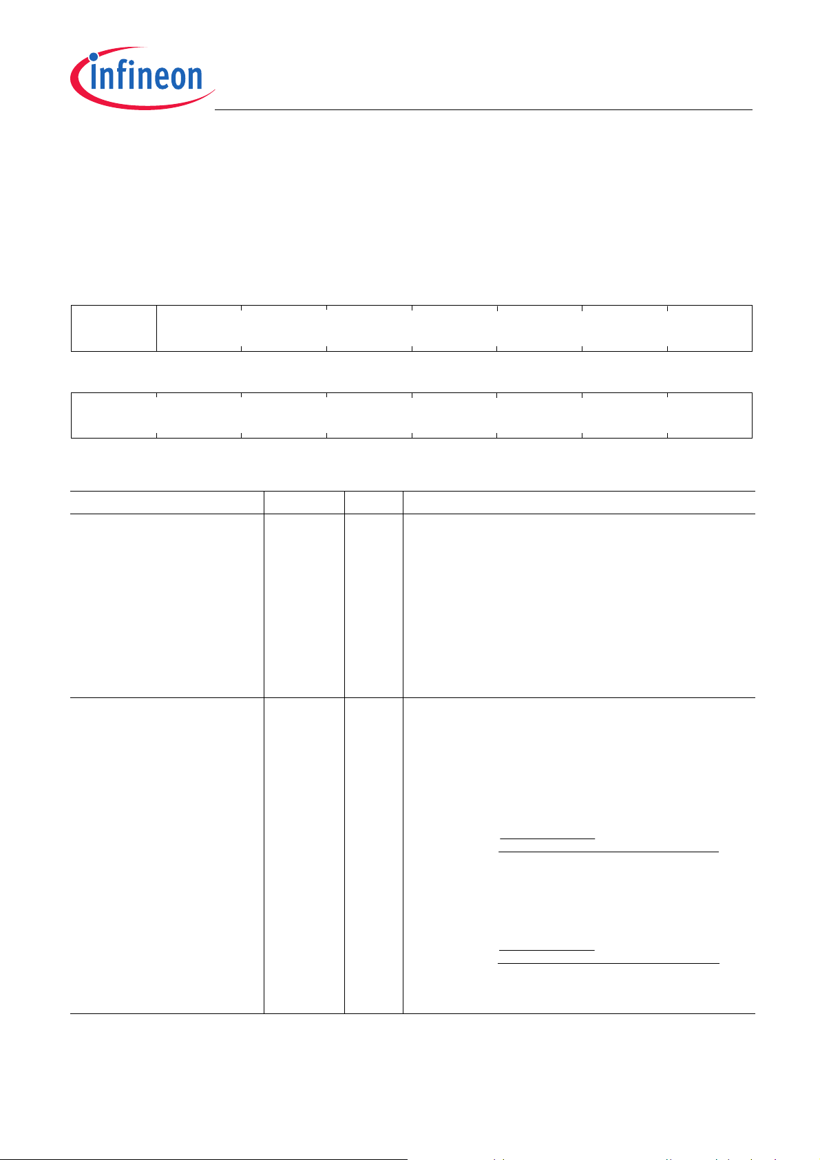
TLE5012B
15 8
7 07 0
RD_AS
14
ru ru
ANG_SPD
ANG_SPD
ru
][2
][_
2
][
]/[
15
st
digitsSPDANG
AngleRange
sSpeed
upd
=°
][3
][_
2
][
]/[
15
st
digi tsSPDANG
AngleRange
sSpeed
upd
=°
SSC Registers
Angle Speed Register
ASPD Offset Reset Value
Angle Speed Register 03
H
8000
Field Bits Type Description
RD_AS 15 r Read Status, Angle Speed
0
no new angle speed value since last readout
B
1
new angle speed value (ANG_SPD) present. The
B
bit is cleared on a read-out (valid for both: normal
operation and update buffer). Note: If an update
event (register snapshot) is done after a normal
read, RD_AS will not be set to 1
in the following
B
read (either update read or normal read) unless a
new value is available.
Reset: 1
B
ANG_SPD 14:0 ru Calculated Angle Speed
Signed value, where the sign bit [14] indicates the
direction of the rotation.
Without prediction difference between the current
unpredicted angle value and second-to-last unpredicted
angle values.
H
°
With prediction, difference between the current predicted
value and second-to-last unpredicted angle value.
°
Reset: 0
H
User’s Manual 82 Rev. 1.2, 2018-02
(6.5)
(6.6)

TLE5012B
15 8
7 07 0
RD_REV
14
ru wu
FCNT
REVOL
ru
ru
REVOL
9
SSC Registers
Angle Revolution Register
AREV Offset Reset Value
Angle Revolution Register 04
H
8000
Field Bits Type Description
RD_REV 15 r Read Status, Revolution
0
no new values since last readout
B
1
new value (REVOL) present. The bit is cleared on
B
a read-out (volid for both: normal operation and
update buffer). Note: If an update event (register
snapshot) is done after a normal read, RD_REV will
not be set to 1
in the following read (either update
B
read or normal read) unless a new value is
available.
Reset: 1
B
FCNT 14:9 wu Frame Counter (unsigned 6-bit value)
Internal frame counter. Increments every update period
(FIR_MD setting).
Reset: 0
H
REVOL 8:0 ru Number of Revolutions (signed 9-bit value)
Revolution counter. Increments for every full rotation in
counter-clockwise direction (at angle discontinuity from
360° to 0°) and decrements for every full rotation in
clockwise direction (at angle discontinuity from 0° to
360°). Also see Chapter 4.2.
Reset: 0
H
H
User’s Manual 83 Rev. 1.2, 2018-02

TLE5012B
15 8
7 0
15 9
wu
FSYNC
8
ru
TEMPER
7 0
ru
TEMPER
SSC Registers
Frame Synchronization Register
FSYNC Offset Reset Value
Frame Synchronization Register 05
H
0000
Field Bits Type Description
FSYNC 15:9 wu Frame Synchronization Counter Value
Subcounter within one frame. Increments every internal
clock cycle (synchronously at a 750kHz rate). Maximum
counter value depends on FIR_MD setting: 16 @
FIR_MD=00; 32 @ FIR_MD=01; 64 @ FIR_MD=10; 128
@ FIR_MD=11.
Reset: 0
H
TEMPER 8:0 ru Temperature Value
Signed offset compensated temperature value. Saturated
below approx. -30°C and above approx. +140°C.
Compensation done by DSPU from T_RAW and the
offset temperature T25O.
T[°C] = (TEMPER[dig]+161[dig]) / 2.776[dig/°C]
For reference point on the real temperature the voltage
via the ESD diode at V
pin is used. This introduces
DD
some variation from device to device. After
characterization, a 9-bit correction is considered more
accurate to extract the temperature:
T[°C] = (TEMPER[dig]+152[dig]) / 2.776[dig/°C]
Reset: 0
H
H
User’s Manual 84 Rev. 1.2, 2018-02

TLE5012B
15 8
7 0
15 14
w
FIR_MD
13
Res
75
Res
44
w
CLK_SEL
33
Res
22
w
DSPU_HO
LD
10
w
IIF_MOD
SSC Registers
Interface Mode1 Register
MOD_1 Offset Reset Value
Interface Mode1 Register 06
H
derivate-specific
Field Bits Type Description
FIR_MD 15:14 w Update Rate Setting (Filter Decimation)
01
42.7 µs
B
10
85.3 µs
B
11
170.6 µs
B
Reset: derivate-specific
CLK_SEL 4 w Clock Source Select
Switch to external clock at start-up only. If there is no
clock signal on the IFC pin when the chip is switched to
the external clock source, the chip does not allow the
switch (CLK_SEL remains zero, operation continued). If
the external clock disappears with CLK_SEL already set,
the chip will reset (PLL out of lock) and run on with the
internal clock.
0
internal oscillator
B
1
external 4-MHz clock (IFC pin switched to input)
B
Reset: 0
DSPU_HOLD 2 w Hold DSPU Operation
B
1)
If DSPU is on hold, no watchdog reset is performed by
DSPU. Deactivate watchdog with AS_WD before setting
DSPU on hold.
0
DSPU in normal schedule operation
B
1
DSPU is on hold
B
Reset: 0
B
IIF_MOD 1:0 w Incremental Interface Mode
00
IIF disabled
B
01
A/B operation with Index on IFC pin
1) DSPU_HOLD is ignored in PWM or SPC mode.
User’s Manual 85 Rev. 1.2, 2018-02
B
10
Step/Direction operation with Index on IFC pin
B
11
not allowed
B
Reset: derivate-specific

TLE5012B
15 8
7 0
1515
w
FILT_PA
R
1414
w
FILT_IN
V
13 11
Res
1010
w
FUSE_RE
L
9
Res
77
Res
66
w
ADCTV_E
N
53
w
ADCTV_Y
20
w
ADCTV_X
SSC Registers
External Clock Selection:
External clock operation is possible for the interface configurations SSC only, SSC & PWM, and SSC& SPC. To
switch the TLE5012B to external clock, the following procedure is used:
• Trigger a chip reset by writing a “1” to the AS_RST bit (address 01
• Within 120 µs after the reset command, write a “1” to the CLK_SEL bit (address 06
[0]) via SSC interface
H
[4])
H
• After the power-on time (max. 7 ms), read the CLK_SEL bit via SSC interface to confirm that external clock is
selected
Note: If the clock source (CLK_SEL) bit is switched to external clock during operation of the sensor without a reset
it may occur, due to an internal timing conflict, that the switching command is not accepted and the chip
keeps operating on internal clock.
SIL Register
SIL Offset Reset Value
SIL Register 07
H
0000
H
Field Bits Type Description
FILT_PAR 15 w Filter Parallel
Diagnostic function to test ADCs’ filter. If enabled, the raw
X-signal is routed also to the raw Y-signal input of the
filter so SIN and COS signal should be identical.
0
filter parallel disabled
B
1
filter parallel enabled (source: X-value)
B
Reset: 0
B
FILT_INV 14 w Filter Inverted
Diagnostic function to test ADCs’ filter. If enabled, the Xand Y-signals are inverted. The angle output is then
shifted by 180°.
0
filter inverted disabled
B
1
filter inverted enabled
B
Reset: 0
User’s Manual 86 Rev. 1.2, 2018-02
B

TLE5012B
Field Bits Type Description
FUSE_REL 10 w Fuse Reload
Triggers reload of default values from laser fuses into
configuration registers.
0
normal operation
B
1
reload of registers with fuse values immediately.
B
Reloaded fuse values are used with the start of the
next filter cycle.
Reset: 0
B
ADCTV_EN 6 w ADC-Test Vectors
Diagnostic function to test ADCs. If enabled, sensor
elements are internally disconnected and test voltages
are connected to ADCs. NO_GMR_A and NO_GMR_XY
status flags will be set to “1”, if this bit is set during
operation. Test vectors can be selected via the register
ADCTV_Y and ADCTV_X.
0
ADC-Test Vectors disabled
B
1
ADC-Test Vectors enabled
B
Reset: 0
B
ADCTV_Y 5:3 w Test vector Y
000
0V
B
001
+70%
B
010
+100%
B
011
+Overflow
B
101
-70%
B
110
-100%
B
111
-Overflow
B
Reset: 0
H
ADCTV_X 2:0 w Test vector X
000
0V
B
001
+70%
B
+100%
010
B
011
+Overflow
B
101
-70%
B
110
-100%
B
111
-Overflow
B
Reset: 0
H
SSC Registers
User’s Manual 87 Rev. 1.2, 2018-02

TLE5012B
15 8
7 0
1515
Res
14
w
ANG_RANGE
74
w
ANG_RANGE
33
w
ANG_DIR
22
w
PREDICT
10
w
AUTOCAL
SSC Registers
Interface Mode2 Register
MOD_2 Offset Reset Value
Interface Mode2 Register 08
H
derivate-specific
Field Bits Type Description
ANG_RANGE 14:4 w Angle Range
1)
Changes the representation of the angle output (AVAL
and ASPD register) by multiplying the output with a factor
ANG_RANGE/128.
080
factor 1 (default), magnetic angle -180°..180°
H
mapped to values -16384..16383
200
factor 4, magnetic angle -45°..45° mapped to
H
values -16384..16383. Values outside this range
are clamped to the limit value and S_OV flag is set.
040
factor 0.5, magnetic angle -180°..180° mapped to
H
values -8192..8191)
Reset: 080
H
ANG_DIR 3 w Angle Direction
Inverts angle and angle speed values and revolution
counter behaviour.
Note: In case of changing ANG_DIR, AUTOCAL should
be deactivated as explained under Note on
Page 23.
0
counterclockwise rotation of magnet
B
1
clockwise rotation of magnet
B
Reset: 0
B
User’s Manual 88 Rev. 1.2, 2018-02

TLE5012B
SSC Registers
Field Bits Type Description
PREDICT 2 w Prediction
Prediction of angle value based on current angle speed
(see data sheet).
Note: In case of changing a PREDICT, AUTOCAL should
be deactivated as explained under Note on
Page 23.
0
prediction disabled
B
1
prediction enabled
B
Reset: derivate-specific
AUTOCAL 1:0 w Autocalibration Mode
Automatic calibration of offset and amplitude
synchronicity for applications with full-turn. Only 1 LSB
corrected at each update. CRC check of calibration
registers is automatically disabled if AUTOCAL activated.
Autocalibration is described in the data sheet. Also see
Chapter 4.1.
00
no auto-calibration
B
01
auto-cal. mode 1: update every angle update cycle
B
(FIR_MD setting)
10
auto-cal. mode 2: update every 1.5 revolutions
B
11
auto-cal. mode 3: update every 11.25°
B
Reset: derivate-specific
1) Autocalibration and Revolution Counter work only for ANG_RANGE = 080H. Activated autocalibration forces 360° angle
range regardless of ANG_RANGE setting.
User’s Manual 89 Rev. 1.2, 2018-02

TLE5012B
15 8
7 0
15
w
ANG_BASE
74
w
ANG_BASE
33
w
SPIKEF
22
w
SSC_OD
10
w
PAD_DRV
SSC Registers
Interface Mode3 Register
MOD_3 Offset Reset Value
Interface Mode3 Register 09
H
device-specific
Field Bits Type Description
ANG_BASE 15:4 w Angle Base
Sets the 0° angle position (12 bit value). Angle base is
factory-calibrated to make the 0° direction parallel to the
edge of the chip.
800
-180°
H
000
0°
H
7FF
+179.912°
H
Reset: device-specific
SPIKEF 3 w Analog Spike Filter of Input Pads
Filters voltage spikes on input pads (IFC, SCK and CSQ).
Additional delay of 10 µs for data input.
0
spike filter disabled
B
1
spike filter enabled
B
Reset: derivate-specific
SSC_OD 2 w SSC-Interface Data Pin Output Mode
0
Push-Pull
B
1
Open Drain
B
Reset: 0
B
PAD_DRV 1:0 w Configuration of Pad-Driver
00
IFA/IFB/IFC: strong driver, DATA: strong driver,
B
fast edge
01
IFA/IFB/IFC: strong driver, DATA: strong driver,
B
slow edge
10
IFA/IFB/IFC: weak driver, DATA: medium driver,
B
fast edge
11
IFA/IFB/IFC: weak driver, DATA: weak driver, slow
B
edge
Reset: derivate-specific
User’s Manual 90 Rev. 1.2, 2018-02

TLE5012B
15 8
7 0
15
w
X_OFFSET
74
w
X_OFFSET
30
Res
15 8
7 0
15
w
Y_OFFSET
74
w
Y_OFFSET
30
Res
SSC Registers
Offset X Register
OFFX Offset Reset Value
Offset X 0A
H
device-specific
Field Bits Type Description
X_OFFSET 15:4 w Offset Correction of X-value in digits
12-bit signed integer value of raw X-signal offset
correction at 25°C.
Reset: device-specific
Offset Y Register
OFFY Offset Reset Value
Offset Y 0B
H
device-specific
Field Bits Type Description
Y_OFFSET 15:4 w Offset Correction of Y-value in digits
12-bit signed integer value of raw Y-signal offset
correction at 25°C.
Reset: device-specific
User’s Manual 91 Rev. 1.2, 2018-02

TLE5012B
15 8
7 0
15
w
SYNCH
74
w
SYNCH
30
Res
SSC Registers
Synchronicity Register
SYNCH Offset Reset Value
Synchronicity 0C
H
device-specific
Field Bits Type Description
SYNCH 15:4 w Amplitude Synchronicity
12-bit signed integer value of amplitude synchronicity
correction (raw X amplitude divided by raw Y amplitude).
For synchronicity correction, the offset compensated Y
value is multiplied by SYNCH.
+2047
0
-2048
D
112.494%
D
100%
87.500%
D
Reset: device-specific
User’s Manual 92 Rev. 1.2, 2018-02

TLE5012B
15 8
7 0
15
w
ORTHO
74
w
ORTHO
33
w
FIR_UDR
22
w
IFAB_OD
10
w
IFAB_HYST
SSC Registers
IFAB Register (multi-purpose)
IFAB Offset Reset Value
IFAB Register 0D
H
device-specific
Field Bits Type Description
ORTHO 15:4 w Orthogonality Correction of X and Y Components
12-bit signed integer value of orthogonality correction.
GMR element orthogonality correction.
+2047
0
-2048
D
11.2445°
D
0°
-11.2500°
D
Reset: device-specific
FIR_UDR 3 w FIR Update Rate
Initial filter update rate (FIR) setting to be loaded into
FIR_MD on startup. Changing of the FIR setting can only
be done by writing to the FIR_MD bits via SPI after
power-on.
0
FIR_MD = ‘10’ (85.3 µs)
B
1
FIR_MD = ‘01’ (42.7 µs)
B
Reset: derivate-specific
IFAB_OD 2 w IFA,IFB,IFC Output Mode
0
Push-Pull
B
1
Open Drain
B
Reset: derivate-specific
User’s Manual 93 Rev. 1.2, 2018-02

TLE5012B
15 8
7 0
15 9
w
TCO_X_T
8
w
HSM_PL
P
75
w
HSM_PLP
43
w
IFAB_RES
22
Res
10
w
IF_MD
SSC Registers
Field Bits Type Description
IFAB_HYST (multi-purpose) 1:0 w HSM and IIF Mode: Hysteresis
Switching hysteresis on direction change for HSM and IIF
interface.
00
0°
B
01
0.175°
B
10
0.35°
B
11
0.70°
B
SPC Mode: Unit Time
00
3.0 µs
B
01
2.5 µs
B
10
2.0 µs
B
11
1.5 µs
B
Reset: derivate-specific
Interface Mode4 Register (multi-purpose)
MOD_4 Offset Reset Value
Interface Mode4 Register 0E
H
device-specific
Field Bits Type Description
TCO_X_T 15:9 w Offset Temperature Coefficient for X-Component
7-bit signed integer value of X-offset temperature
coefficient. This register is used both with autocalibration
and without autocalibration. If autocalibration is
deactivated, overwrite only with the default value. If
autocalibration is activated, do not write this bitfield. See
“Offset temperature compensation” on Page 97.
Reset: device-specific
User’s Manual 94 Rev. 1.2, 2018-02

TLE5012B
SSC Registers
Field Bits Type Description
HSM_PLP (multi-purpose) 8:5 w Hall Switch Mode: Pole-Pair Configuration
0000
1 pole pairs
B
0001
2 pole pairs
B
0010
3 pole pairs
B
...
...
B
1101
14 pole pairs
B
1110
15 pole pairs
B
1111
16 pole pairs
B
Pulse-Width-Modulation Mode: Error Indication
xx0x
error indication enabled
B
xx1x
error indication disabled
B
Incremental Interface Mode: Absolute Count
Interface counts to absolute value at startup
absolute count enabled
x0xx
B
x1xx
absolute count disabled
B
SPC Mode: Total Trigger Time
Duration of the master pulse to trigger SPC output
0000
90*UT
B
0100
B tmlow
+ 12 UT
Reset: derivate-specific
IFAB_RES (multi-purpose) 4:3 w Pulse-Width-Modulation Mode: Frequency
Selection of PWM frequency.
00
244 Hz
B
01
488 Hz
B
10
977 Hz
B
1953 Hz
11
B
Incremental Interface Mode: IIF resolution
12bit, 0.088° step
00
B
01
11bit, 0.176° step
B
10
10bit, 0.352° step
B
11
9bit, 0.703° step
B
SPC Mode: SPC Frame Configuration
12bit angle
00
B
01
16bit angle
B
10
12bit angle + 8bit temperature
B
11
16bit angle + 8bit temperature
B
Reset: derivate-specific
User’s Manual 95 Rev. 1.2, 2018-02

TLE5012B
Sync hronis ation Fr ame St atus -N ibble D ata- Nibbl es
56 tck 12 ..27 tck 12.. 27 tck
Ti m e-Base : 1 tck (3µ s+/ -d tck )
Trigger Nibble
24,34 ,51,78 tck
µC Activity
Sensor Activi ty
angle calculation
...
SSC Registers
Field Bits Type Description
IF_MD 1:0 w Interface Mode on IFA,IFB,IFC
Any derivate can be configurated to operate in any of the
four following protocols on the IFA, IFB and IFC outputs.
Reconfiguration is required at every start-up, else the
default protocol of the derivate will be used.
SSC interface is always active in parallel on pins SCK,
CSQ and DATA.
00
IIF
B
01
PWM
B
10
HSM
11
B
B
SPC
1)
Reset: derivate-specific
1) In SPC interface configuration, the sensor’s digital signal processing unit (DSPU) runs only when receiving a SPC trigger
pulse on the IFA pin (see Figure 6-12). This means that changes to register settings are applied and also the angle (AVAL)
register is updated only after a trigger pulse.
Figure 6-12 Timing of angle calculation in SPC. Trigger Nibble low time corresponds to slave number.
User’s Manual 96 Rev. 1.2, 2018-02

TLE5012B
15 015 9
w
TCO_Y_T
88
w
SBIS
T
70
w
CRC_PAR
Offset_X/Y[T] = Offset_X/Y[25°C] + (TCO_X/Y_T*(TEMPER[T]-TEMPER[25°C]))/128
SSC Registers
Temperature Coefficient Register
TCO_Y Offset Reset Value
Temperature Coefficient Register 0F
H
device-specific
Field Bits Type Description
TCO_Y_T 15:9 w Offset Temperature Coefficient for Y-Component
7-bit signed integer value of Y-offset temperature
coefficient. This register is used both with autocalibration
and without autocalibration. If autocalibration is
deactivated, overwrite only with the default value. If
autocalibration is activated, do not write this bitfield. See
“Offset temperature compensation” on Page 97.
Reset: device-specific
SBIST 8 w Startup-BIST
0
Startup-BIST disabled
B
1
Startup-BIST enabled
B
Reset: 1
B
CRC_PAR 7:0 w CRC of Parameters
CRC of parameters from address 08
to 0FH. If any
H
settings within these registers are changed, this CRC has
to be changed accordingly.
Reset: device-specific
Offset temperature compensation
The TLE5012B compensates the temperature dependence of the X- and Y-offsets during run-time by using an
integrated temperature measurement (see register TEMPER on Page 84) and applying factory-calibrated
temperature coefficients for the offsets. At a chip temperature of T, the resulting offset correction parameters are
given by:
Temperature compensation of the offsets is only active, if autocalibration is disabled. If auto-calibration is enabled,
TCO_X_T and TCO_Y_T are automatically set to 0. Once auto-calibration is deactivated, laser-fused calibration
values are loaded into TCO_X_T and TCO_Y_T.
User’s Manual 97 Rev. 1.2, 2018-02
(6.7)

TLE5012B
15 015 0
r
ADC_X
15 015 0
r
ADC_Y
SSC Registers
X-raw Value Register
ADC_X Offset Reset Value
X-raw value 10
H
0000
Field Bits Type Description
ADC_X 15:0 r ADC value of X-GMR
16-bit signed integer raw X value. Read-out of this
register will update ADC_Y
Reset: 0
H
H
Y-raw Value Register
ADC_Y Offset Reset Value
Y-raw value 11
H
0000
Field Bits Type Description
ADC_Y 15:0 r ADC value of Y-GMR
16-bit signed integer raw Y value. Updated when ADC_X
or ADC_Y is read.
Reset: 0
H
H
User’s Manual 98 Rev. 1.2, 2018-02

TLE5012B
15 8
7 0
1515 14 13
Res
1212 1111 1010 99
ru
MAG
88
77665544
ru
332211 00
MAG
SSC Registers
D_MAG Register
D_MAG Offset Reset Value
D_MAG Register 14
H
0000
Field Bits Type Description
MAG 9:0 ru Angle Vector Magnitude
Unsigned Angle Vector Magnitude after X, Y error
compensation (due to temperature).
This field allows additional safety checks.
Formula:
MAG = (SQRT(X*X+Y*Y))/64
Reset: 0
H
H
User’s Manual 99 Rev. 1.2, 2018-02

TLE5012B
15 8
7 0
1515
ru
T_TGL
14 13 1212 1111 1010 99
ru
T_RAW
88
77665544
ru
332211 00
T_RAW
Res
SSC Registers
T_RAW Register
T_RAW Offset Reset Value
T_RAW Register 15
H
0000
Field Bits Type Description
T_TGL 15 ru Temperature Sensor Raw-Value Toggle
Toggles after every new temperature value (T_RAW).
Reset: 0
B
T_RAW 9:0 ru Temperature Sensor Raw-Value
Temperature at ADC. This value is not compensated with
the offset temperature. T_RAW range is not limited as
TEMPER. T_RAW is an unsigned value.
T[°C]=(T_RAW[dig]-369[dig]-T25O[dig]) / 2.776[dig/°C]
Reset: 0
H
H
User’s Manual 100 Rev. 1.2, 2018-02
 Loading...