

Microcomputer Components
SAB 80C515A/83C515A-5
8-Bit CMOS Single-Chip Microcontroller Family
Addendum to User's Manual SAB 80515/80C515 08.95

SAB 80C515A/83C515A-5 Addendum
Revision History: Current Version: 08.95
Previous Version: 11.92
Page Subjects (major changes since last revision)
3-6
3-16
5-4
5-10
CCH4 / CCL4 deleted
Table supplemented (MOVX @Ri, EA
Falling edge for P4.0 / ADST
in figure 5-2 added
Formula for SREL added
= 1, 00)
6-1 New release of SAB 80C515A / 83C515A-5 data sheet inserted
Edition 08.95
Published by Siemens AG,
Bereich Halbleiter, Marketing-
Kommunikation, Balanstraße 73,
81541 München
©
Siemens AG 1995.
All Rights Reserved.
Attention please!
As far as patents or other rights of third parties are conc erned, liability is only assumed for components, not for applic ations, processes
and circuits implemented within components or assemblies.
The information describes the type of component and shall not be conside red as as sured characteristics.
Terms of delivery and rights to change design res erved.
For questions on technology, delivery and prices please contact the Semiconductor Group Offices in Germany or the Siemens Companies
and Representatives worldwide (see address list).
Due to technical requirements components m ay contain dangerous substances. For information on the types in question please contact
your nearest Siemens Office, Sem iconductor Group.
Siemens AG is an approved CECC manufacturer.
Packing
Please use the recycling operators know n to you. We can also help you – get in touch with your near est sales office. By agreement we
will take packing material back, if it is sorted. You must bear the costs of transport.
For packing material that is returned to us unsorted or which we are not obliged to accept, we shall have to invoice you for any costs incurred.
Components used in life-support devices or systems must be expressly authorized for such purpose!
Critical components
written approval of the Semiconductor Group of Siemens AG.
1 A critical component is a component used in a life-support device or system whose failure can reasonably be expected to cause the
failure of that life-support device or system, or to affect its safet y or ef fectiv eness of that device or system.
2 Life support devices or systems are intended (a) to be implante d in the human body, or (b) to su pport and/o r maintain a nd sustain hu-
man life. If they fail, it is reasonable to assume that the health of the user may be endangered.
1
of the Semiconductor Group of Siemens AG, may only be used in life-support devices or systems2 with the express

SAB 80C515A/83C515A
Table of Contents Page
1 Introduction . . . . . . . . . . . . . . . . . . . . . . . . . . . . . . . . . . . . . . . . . . . . . . . . 1-1
2 Fundamental Structure . . . . . . . . . . . . . . . . . . . . . . . . . . . . . . . . . . . . . . . 2-1
3 Memory Organization . . . . . . . . . . . . . . . . . . . . . . . . . . . . . . . . . . . . . . . . 3-1
3.1 Program Memory, ROM Protection . . . . . . . . . . . . . . . . . . . . . . . . . . . . . . . 3-2
3.2 Data Memory . . . . . . . . . . . . . . . . . . . . . . . . . . . . . . . . . . . . . . . . . . . . . . . . 3-3
3.3 Special Function Registers . . . . . . . . . . . . . . . . . . . . . . . . . . . . . . . . . . . . . 3-3
3.4 Architecture of the XRAM. . . . . . . . . . . . . . . . . . . . . . . . . . . . . . . . . . . . . . . 3-8
3.4.1 Accesses to XRAM . . . . . . . . . . . . . . . . . . . . . . . . . . . . . . . . . . . . . . . . . . . 3-8
3.4.2 Control of XRAM in the SAB 80C515A . . . . . . . . . . . . . . . . . . . . . . . . . . . 3-14
3.4.3 Behaviour of Port0 and Port2 . . . . . . . . . . . . . . . . . . . . . . . . . . . . . . . . . . . 3-15
4 System Reset . . . . . . . . . . . . . . . . . . . . . . . . . . . . . . . . . . . . . . . . . . . . . . . 4-1
4.1 Additional Hardware Power Down Mode in the SAB 80C515A . . . . . . . . . . 4-1
4.2 Hardware Power Down Reset Timing . . . . . . . . . . . . . . . . . . . . . . . . . . . . . 4-4
4.3 Fast Internal Reset after Power-On . . . . . . . . . . . . . . . . . . . . . . . . . . . . . . . 4-8
5 On-Chip Peripheral Components . . . . . . . . . . . . . . . . . . . . . . . . . . . . . . . 5-1
5.1 10-Bit A/D-Converter . . . . . . . . . . . . . . . . . . . . . . . . . . . . . . . . . . . . . . . . . . 5-3
5.2 New Baud Rate Generator for Serial Channel . . . . . . . . . . . . . . . . . . . . . . . 5-8
5.3 Fail Save Mechanisms . . . . . . . . . . . . . . . . . . . . . . . . . . . . . . . . . . . . . . . . 5-11
5.3.1 Programmable Watchdog Timer . . . . . . . . . . . . . . . . . . . . . . . . . . . . . . . . 5-12
5.3.2 Oscillator Watchdog Unit . . . . . . . . . . . . . . . . . . . . . . . . . . . . . . . . . . . . . . 5-17
6 Devices Specifications . . . . . . . . . . . . . . . . . . . . . . . . . . . . . . . . . . . . . . . . 6-1
Semiconductor Group I-1

Introduction
1 Introduction
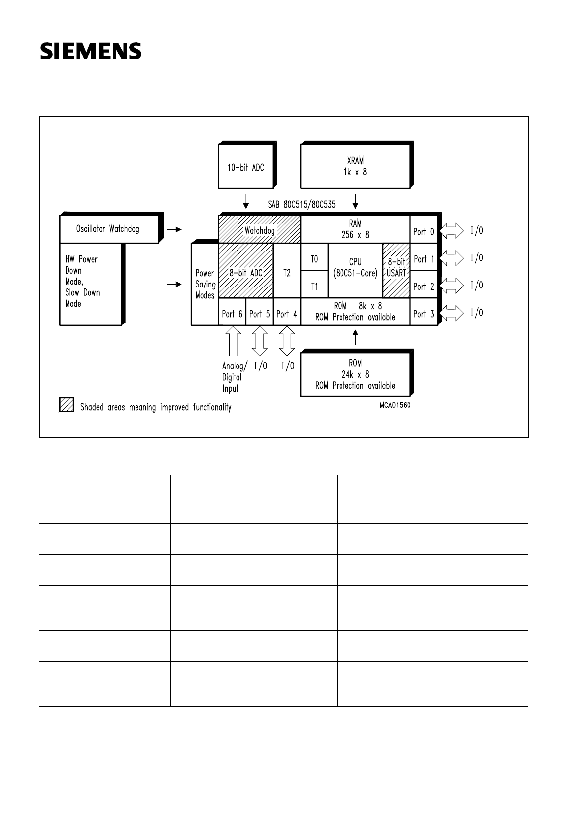
The SAB 80C515A is a superset of the high end microcontroller SAB 80C515.
While maintain ing all architectural and operat ional characteristics of the SA B 80C515 t he
SAB 80C515A incorporates more on-chip RAM. A new 10-bit A/D-Converter is implemented as well
as an oscillator watchdog unit. Also the operating frequency is higher than at the SAB 80C515.
SAB 80C515A / 83C515A-5
Semiconductor Group 1-1

Introduction
The SAB 80C515A is available in two different versions:
– "ROMless" Version SAB 80C515A. Although this part is called "ROMless" there is an internal
ROM of 2 KByte (for Test and Loader Software)
– ROM Version SAB 83C515A-5. This part has 32 KByte on-chip ROM.
With exception of the ROM sizes both parts are identical. Therefore the term SAB 80C515A refers
to both versions within this specification unless otherwise noted.
This manual describes only the new features of the SAB 80C515A in addition to the features of the
SAB 80C515/80C535. For reference to the SAB 80C515, the user's manual should be used.
Listed below is a summary of the main features of the SAB 80C515A:
● SAB 80C515A/83C515A-5, up to
18 MHz operation frequency
● 32 K × 8 ROM (SAB 83C515A-5 only, ROM-
Protection available)
● 256 × 8 on-chip RAM
● additional 1 K × 8 on-chip RAM (XRAM)
● Superset of SAB 80C51 architecture:
–1 µs instruction cycle time at 12 MHz
– 666 ns instruction cycle time at 18 MHz
– 256 directly addressable bits
● Boolean processor
● 64 Kbyte external data and program memory
addressing
● Three 16-bit timer/counters
● Versatile "fail-safe" provisions
● 12 interrupt vectors, four priority levels
selectable
● genuine 10-bit A/D converter with 8
multiplexed inputs
● Full duplex serial interface with
programmable Baudrate-Generator
● Functionally compatible with SAB 80C515
● Extended power saving modes
● Fast Power-On Reset
● Six ports: 48 I/O lines, 8 input lines
● Three temperature ranges available:
0 to 70 °C(T1)
– 40 to + 85 °C(T3)
– 40 to + 110 °C(T4)
●Plastic package: P-LCC-68
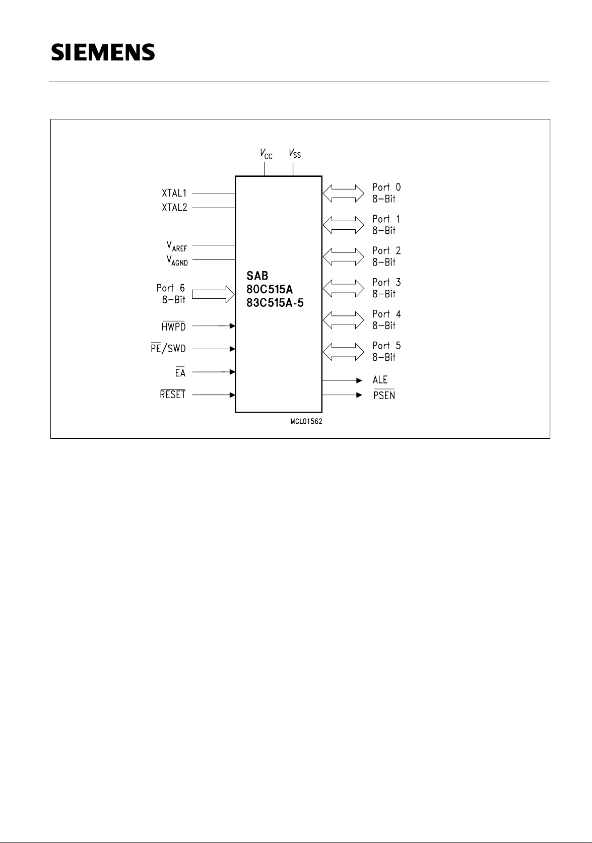
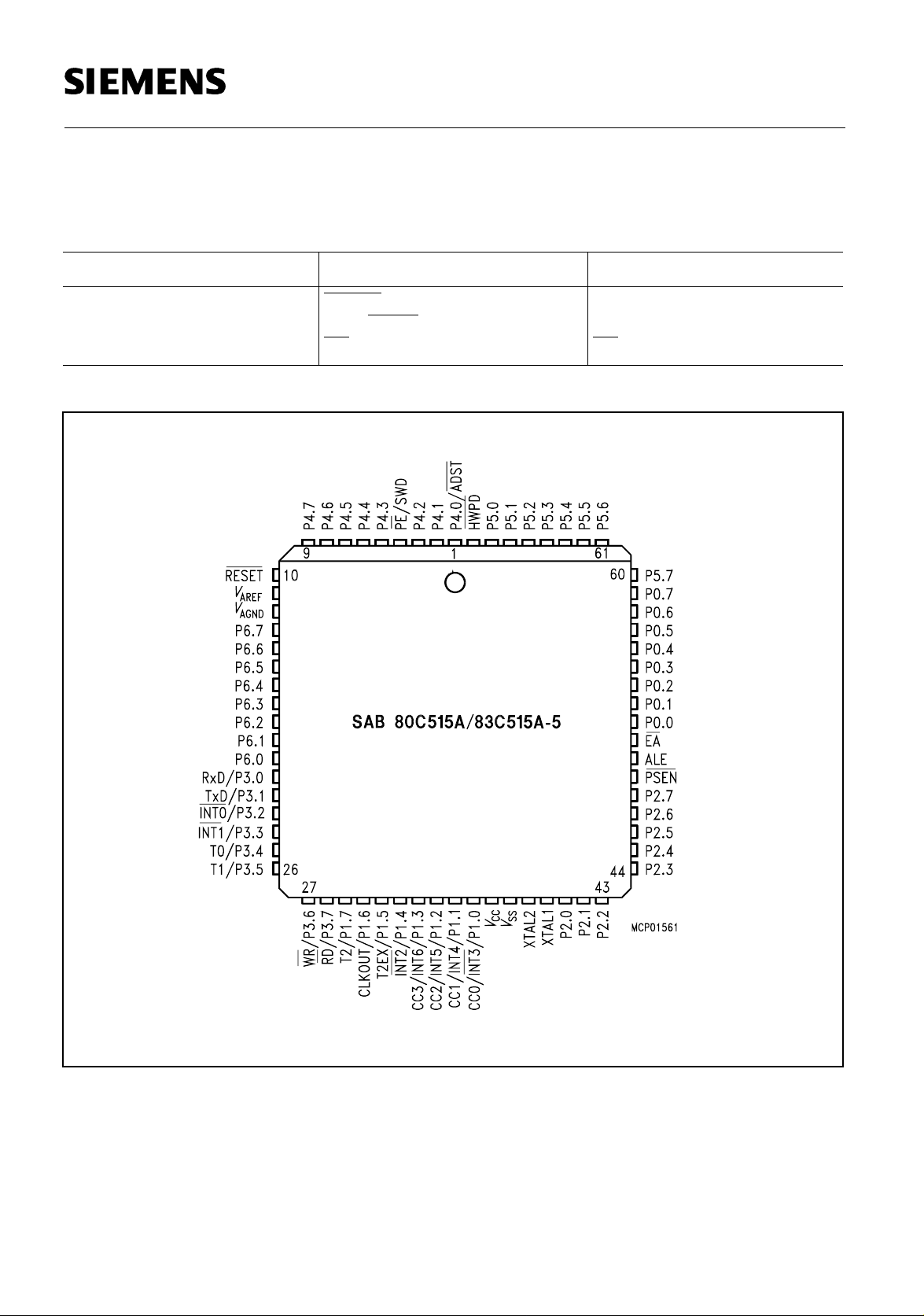
The pin functions of the SAB 80C515A are identical with those of the SAB 80C515 with following
exceptions:
SAB 80C515A SAB 80C515
Pin 68 HWPD
V
CC
Pin 1 P4.0/ADST P4.0
Pin 4 PE
/SWD PE
Semiconductor Group 1-2

2 Fundamental Structure
Fundamental Structure
The SAB
family. It is designe d in Siemens ACMOS techn ology and based on the S AB8051 architecture.
ACMOS is a technology which combines high-speed and density characteristics with low-power
consumption or dissipation.
While maintaining all the SAB 80C515 features and operating characteristics the SAB80C515A/
83C515A-5 contains more on-chip RAM/ROM. Further more a new 10-bit A/D-Converter is
implemented as well as extended security mechanisms.
SAB 83C515A-5 except
83C515A-5 is supplied in a 68-pin plastic leaded chip carrier package (P-LCC-68).
The essential enhancements to the SAB 80C515 are (see also figure 2-1):
– Additional 1KByte RAM on chip
– 8-Channel 10-bit A/D Converter
– New baud rate generator for the Serial Channel
– Oscillator Watchdog Unit
– Improved functionality of the Watchdog Timer
– Hardware controlled Power Down Mode
– High speed operation of the device (up to 18 MHz crystal frequency)
80C515A/83C515A-5 is a high-end member of the Siemens SAB 8051 microcontroller
The SAB 80C515A is identical with the
that it lacks the on-chip program memory. The SAB 80C515A/
Semiconductor Group 2-1

Fundamental Structure
Figure 2-1
Block Diagram of the SAB 80C515A / 83C515A-5
Semiconductor Group 2-2

Memory Organization
3 Memory Organization
According to the SAB 8051 architecture, the SAB 80C515A has separate address spaces for
program and data memory. Figure 3-1 illustrates the mapping of address spaces.
Figure 3-1
Memory Map
Semiconductor Group 3-1

Memory Organization
3.1 Program Memory, ROM Protection
The
SAB 83C515A-5 has 32 Kbyte of on-chip ROM, while the SAB 80C515A has no internal
ROM. The program memory can externally be expanded up to 64 Kbyte. Pin EA
whether program fetches below address 8000H are done from internal or external memory.
As a new feature the SAB 83C515A-5 offers the possibility of protecting the internal ROM against
unauthorized access. This protection is implemented in the ROM-Mask. Therefore, the decision
ROM-Protection ’yes’ or ’no’ has to be made when delivering the ROM-Code. Once enabled, there
is no way of disabling the ROM-Protection.
Effect: The access to internal ROM done by an externally fetched MOVC instruction is disabled.
Nevertheless, an access from internal ROM to external ROM is possible.
To verify the read protected ROM-Code a special ROM-Verify-Mode is implemented. This mode
also can be used to verify unprotected internal ROM.
determines
ROM-Protection ROM-Verification Mode
(see ’AC Characteristics’)
no ROM-Verification Mode 1
(standard 8051 Verification Mode)
ROM-Verification Mode 2
yes ROM-Verification Mode 2 – standard 8051
Restrictions
–
Verification Mode is
disabled
– externally applied MOVC
accessing internal ROM is
disabled
Semiconductor Group 3-2

Memory Organization
3.2 Data Memory
The data memory space consists of an internal and a n external memory spa ce. The SAB 80C515A
contains another 1 kByte of On-Chip RAM additional to the 256 Bytes internal RAM of the base typ e
SAB 80C515. This RAM is called XRAM (’eXtended RAM’) in this document.
– External Data Memory
Up to 64 Kbyte external data memory can be addressed by instructions that use 8-bit or 16bit indirect addressing. For 8-bit addressing MOVX instructions in combination with registers
R0 and R1 can be used. A 16-bit external memory addressing is supported by a 16-bit
datapointer. Registers XPAGE and SYSCON are controlling whether data fetches at
addresses F800H to FBFFH are done from internal XRAM or from external data memory.
– Internal Data Memory
The internal data memory is divided into four physically distinct blocks:
– the lower 128 bytes of RAM including four register banks containing eight registers each
– the upper 128 byte of RAM
– the 128 byte special function register area
– a 1Kx8 area which is accessed like external RAM (MOVX-instructions), implemented on
chip at the address range from F800H to FBFFH. Special Function Register SYSCON
controls whether data is read from or written to XRAM or external RAM.
3.3 Special Function Registers
All registers, except the p rogram counter an d the fou r general purpose regi ster bank s, resid e in th e
special function register area. The special function registers include arithmetic registers, pointers,
and registers that provide an interface between the CPU and the on-chip peripherals. There are
also 128 directly addressable bits within the SFR area.
All special function registers are listed in table 3-1 and table 3-2.
In table 3-1 they are organized in numeric order of thei r addresse s. In table 3-2 the y are org anized
in groups which refer to the functional blocks of the SAB 80C515A.
Semiconductor Group 3-3

Table 3-1
Special Function Register
Memory Organization
Address Register Contents
after Reset
1)
80
81
82
83
84
85
86
87
88
89
8A
8B
8C
8D
8E
8F
90
91
92
93
94
95
96
97
98
99
9A
9B
9C
9D
9E
9F
H
H
H
H
H
H
H
H
H
H
H
H
H
H
H
H
H
H
H
H
H
H
H
H
H
H
H
H
H
H
H
H
P0
SP
DPL
DPH
(WDTL)
(WDTH)
WDTREL
PCON
TCON
1)
TMOD
TL0
TL1
TH0
TH1
reserved
reserved
1)
P1
XPAGE
reserved
reserved
reserved
reserved
reserved
reserved
SCON
1)
SBUF
reserved
reserved
reserved
reserved
reserved
reserved
FF
H
07
H
00
H
00
H
00
H
00
H
00
H
00
H
00
H
00
H
00
H
00
H
XX
H
XX
H
FF
H
00
H
XXH
XX
H
XXH
XXH
XX
H
XXH
00
H
XXH
XXH
XX
H
XXH
XXH
XX
H
XXH
2)
2)
2)
2)
2)
2)
2)
2)
2)
2)
2)
2)
2)
2)
2)
Address Register Contents
after Reset
1)
A0
A1
A2
A3
A4
A5
A6
A7
A8
A9
AA
AB
AC
AD
AE
AF
B0
B1
B2
B3
B4
B5
B6
B7
B8
B9
BA
BB
BC
BD
BE
BF
H
H
H
H
H
H
H
H
H
H
H
H
H
H
H
H
H
H
H
H
H
H
H
H
H
H
H
H
H
H
H
H
P2
reserved
reserved
reserved
reserved
reserved
reserved
reserved
1)
IEN0
IP0
SRELL
reserved
reserved
reserved
reserved
reserved
1)
P3
SYSCON
reserved
reserved
reserved
reserved
reserved
reserved
1)
IEN1
IP1
SRELH
reserved
reserved
reserved
reserved
reserved
FF
H
2)
XXH
2)
XXH
2)
XXH
2)
XXH
2)
XXH
2)
XXH
2)
XXH
00
H
00
H
0D9
H
2)
XXH
2)
XXH
2)
XXH
2)
XXH
2)
XXH
FF
H
XXXXXX01
2)
XXH
2)
XXH
2)
XXH
2)
XXH
2)
XXH
2)
XXH
00
H
XX000000
XXXXXX11
2)
XXH
2)
XXH
2)
XXH
2)
XXH
2)
XXH
2)
B
2)
B
2)
B
1) Bit-addressable Speci al Fu nc t ion R egister
2) X means that the value is indete rm inate and the location is reserved
Semiconductor Group 3-4

Table 3-1, Special Function Register (cont’d)
Memory Organization
Address Register Contents
after Reset
C0
C1
C2
C3
C4
C5
C6
C7
C8
C9
CA
CB
CC
CD
CE
CF
D0
D1
D2
D3
D4
D5
D6
D7
D8
D9
DA
DB
DC
DD
DE
DF
H
H
H
H
H
H
H
H
H
H
H
H
H
H
H
H
H
H
H
H
H
H
H
H
H
H
H
H
H
H
H
H
IRCON
CCEN
CCL1
CCH1
CCL2
CCH2
CCL3
CCH3
T2CON
reserved
CRCL
CRCH
TL2
TH2
reserved
reserved
PSW
reserved
reserved
reserved
reserved
reserved
reserved
reserved
ADCON0
ADDATH
ADDATL
P6
ADCON1
reserved
reserved
reserved
1)
1)
1)
1)
00
H
00
H
00
H
00
H
00
H
00
H
00
H
00
H
00
H
XXH
00
H
00
H
00
H
00
H
XXH
XXH
00
H
XX
H
XXH
XX
H
XXH
XX
H
XXH
XX
H
00
H
00
H
00
H
XX
H
2)
2)
2)
2)
2)
2)
2)
2)
2)
2 )
2)
XXXX0000
2)
XX
H
2)
XXH
2)
XX
H
B
Address Register Contents
1)
E0
H
E1
H
E2
H
E3
H
E4
H
E5
H
E6
H
E7
H
E8
H
E9
H
EA
H
EB
H
EC
H
ED
H
EE
H
EF
H
F0
H
F1
H
F2
H
F3
H
F4
H
F5
H
F6
H
F7
H
F8
H
F9
H
FA
H
FB
FC
FD
FE
FF
H
H
H
H
H
2)
ACC
reserved
reserved
reserved
reserved
reserved
reserved
reserved
1)
P4
reserved
reserved
reserved
reserved
reserved
reserved
reserved
1)
B
reserved
reserved
reserved
reserved
reserved
reserved
reserved
1)
P5
reserved
reserved
after Reset
00
H
2)
XX
H
2)
XXH
2)
XX
H
2)
XXH
2)
XX
H
2)
XXH
2 )
XX
H
FF
H
2)
XX
H
2)
XXH
2)
XX
H
2)
XXH
2)
XX
H
2)
XXH
2 )
XX
H
00
H
2)
XX
H
2)
XXH
2)
XX
H
2)
XXH
2)
XX
H
2)
XXH
2 )
XX
H
FF
H
2)
XX
H
2)
XXH
1) Bit-addressable Speci al Fu nc t ion R egister
2) X means that the value is indete rm inate and the location is reserved
Semiconductor Group 3-5

Memory Organization
Table 3-2
Special Function Registers - Functional Blocks
Block Symbol Name Address Contents after
Reset
1)
CPU ACC
B
DPH
DPL
PSW
SP
A/DConverter
ADCON0
ADCON1
ADDATH
ADDATL
Interrupt
IEN0
System
IEN1
Accumulator
B-Register
Data Pointer, High Byte
Data Pointer, Low Byte
Program Status Word Register
Stack Pointer
A/D Converter Control Register 0
A/D Converter Control Register 1
A/D Converter Data Register High Byte
A/D Converter Data Register Low Byte
Interrupt Enable Register 0
Interrupt Enable Register 1
E0H
F0H
83
H
82
H
0D0H
81
H
D8H
0DC
H
0D9
H
0DA
H
A8
H
B8H
00
1)
1)
1)
1)
1)
H
00
H
00
H
00
H
00
H
07
H
00
H
0XXX 0000
00
H
00
H
00
H
00
H
3)
B
IP0
IP1
IRCON
TCON
T2CON
Compare/
CaptureUnit (CCU)
CCEN
CCH1
CCH2
CCH3
CCL1
CCL2
CCL3
CRCH
CRCL
TH2
TL2
T2CON
XRAM XPAGE
SYSCON
Interrupt Priority Register 0
Interrupt Priority Register 1
Interrupt Request Control Register
2)
Timer Control Register
2)
Timer 2 Control Register
Comp./Capture Enable Reg.
Comp./Capture Reg. 1, High Byte
Comp./Capture Reg. 2, High Byte
Comp./Capture Reg. 3, High Byte
Comp./Capture Reg. 1, Low Byte
Comp./Capture Reg. 2, Low Byte
Comp./Capture Reg. 3, Low Byte
Com./Rel./Capt. Reg. High Byte
Com./Rel./Capt. Reg. Low Byte
Timer 2, High Byte
Timer 2, Low Byte
Timer 2 Control Register
Page Addr. Reg. for extended onchip RAM
XRAM Control Reg.
0A9
0B9
C0H
88H
C8H
0C1
0C3
0C5
0C7
0C2
0C4
0C6
0CB
0CA
0CD
0CC
C8H
91
H
0B1
H
H
H
H
H
H
H
H
H
H
H
H
H
H
00
H
XX00 0000
1)
00
H
1)
00
00
00
00
00
00
00
00
00
00
00
00
00
00
00
H
H
H
H
H
H
H
H
H
H
H
H
H
H
H
1)
1)
XXXX XX01
3)
B
3)
B
1) Bit-addressable special f unc t ion registers
2) This special function register is listed repeatedly since some bits of it also belong to other functional blocks.
3) X means that the value is indete rm inate and the location is reserved
Semiconductor Group 3-6

Memory Organization
Table 3-2, Special Function Registers - Functional Blocks (cont’d)
Block Symbol Name Address Contents after
Reset
1)
Ports P0
P1
P2
P3
P4
P5
P6
Power Save
PCON Power Control Register 87
Modes
Serial
Channels
ADCON0
PCON
SBUF
SCON
SRELL
SRELH
Timer 0/
Timer 1
TCON
TH0
TH1
TL0
TL1
TMOD
Watchdog IEN0
IEN1
2)
IP0
2)
IP1
WDTREL
Port 0
Port 1
Port 2
Port 3
Port 4
Port 5
Port 6, Analog/Digital Input
2)
A/D Converter Control Reg.
2)
Power Control Register
Serial Channel Buffer Reg.
Serial Channel Control Reg.
Serial Channel Reload Reg., low byte
Serial Channel Reload Reg., high byte
Timer Control Register
Timer 0, High Byte
Timer 1, High Byte
Timer 0, Low Byte
Timer 1, Low Byte
Timer Mode Register
2)
2)
Interrupt Enable Register 0
Interrupt Enable Register 1
Interrupt Priority Register 0
Interrupt Priority Register 1
Watchdog Timer Reload Reg.
80H
90H
A0H
B0H
E8H
F8H
DB
H
H
0D8
H
87
H
99
H
98
H
AA
H
BA
H
88H
8C
H
8D
H
8A
H
8B
H
89
H
A8
H
B8
H
A9
H
B9
H
86
H
0FF
1
1)
1)
1)
1)
1)
1)
1)
1)
1)
H
0FF
H
0FF
H
0FF
H
0FF
H
0FF
H
00
H
00
H
00
H
0XXH
00
D9
3)
H
H
XXXX XX11
00
H
00
H
00
H
00
H
00
H
00
H
00
H
00
H
00
H
XX00 0000B
00
H
3)
B
3)
1) Bit-addressable special f unc t ion registers
2) This special function register is listed repeatedly since some bits of it also belong to other functional blocks.
3) X means that the value is indete rm inate and the location is reserved
Semiconductor Group 3-7

Memory Organization
3.4 Architecture of the XRAM
The contents of the XRAM is not affected by a reset or HW Power Down. After power-up the
contents is undefined, while it remains unchanged during an d after a reset or HW Power Down if th e
power supply is not turned off.
The additional On-Chip RAM is logically located in the "external data memory" range at the upper
end of the 64 KByte address range (F800H -FBFFH). Nevertheless when XRAM is enabled the
address range F800H to FFFFH is occupied. This is done to assure software compatibility to SAB
80C517A. It is possible to enable and disable (only by reset) the XRAM. If it is disabled the device
shows the same behaviour as the parts without XRAM, i.e. a ll MOVX accesses use the external bus
to physically external data memory.
3.4.1 Accesses to XRAM
Because the XRAM is used in the same way as external data memory the same instruction types
must be used for accessing the XRAM.
Note:
If a reset occurs during a write op eration to XRAM, the effect on XRAM depends on the cycl e which
the reset is detected at (MOVX is a 2-cycle instruction):
Reset detection at cycle 1: The new value will not be written to XRAM. The old value is not
affected.
Reset detection at cycle 2: The old value in XRAM is overwritten by the new value.
Accesses to XRAM using the DPTR
There are a Read and a Write instruction from and to XRAM which use one of the 16-bit DPTR for
indirect addressing. The instructions are:
MOVX A, @DPTR (Read)
MOVX @DPTR, A (Write)
Normally the use of these instructions would use a physically external memory. However, in the
SAB 80C515A the XRAM is accessed if it is enabled and if the DPTR points to the XRAM address
space (DPTR ≥ F800H).
Semiconductor Group 3-8

Memory Organization
Accesses to XRAM using the Registers R0/R1
The 8051 architecture provides also instructions for accesses to external data memory ra nge which
use only an 8-bit address (indirect addressing with registers R0 or R1). The instructions are:
MOVX A, @ Ri (Read)
MOVX @Ri, A (Write)
In application systems, either a real 8-bit bus (with 8-bit address) is used or Port 2 serves as page
register which selects pages of 256-Byt e. However, the distinction, whether Port 2 is used as
general purpose I/0 or as "page address" is mad e by the external system design . From the device’s
point of view it cannot be decided whether the Port 2 data is used externally as address or as I/0
data!
Hence, a special page register is implemented into the SAB 80C515A to provide the possibility of
accessing the XRAM also with the MOVX @Ri instructions, i.e. XPAGE serves the same function
for the XRAM as Port 2 for external data memory.
Special Function Register XPAGE
MSB LSB
Bit No.
Addr.91H
The reset value of XPAGE is 00H.
XPAGE can be set and read by software.
Figures 3-2 to 3-4 show the dependencies of XPAGE- and Port 2 - addressing in order to explain
the differences in accessing XRAM, ext. RAM or what is to do when Port 2 is used as an I/O-port.
76543210
XPAGE
Semiconductor Group 3-9

Memory Organization
Figure 3-2
Write Page Address to Port 2
MOV P2, pageaddress
When external RAM is to be accessed in the XRAM address range (F800H - FFFFH) XRAM has to
be disabled. When additional external RAM is to be addressed in an address range ≤ XRAM
(F800H) XRAM may remain being enabled and there is no need to overwrite XPAGE by a second
move.
Semiconductor Group 3-10
will write the page address to Port 2 and XPAGE-Register.

Memory Organization
Figure 3-3
Write Page Address to XPAGE
The page address is only written to XPAGE-register. Port 2 is available for addresses or I/O-Data.
See figure 3-4 to see what happens when Port 2 is used as I/O-Port.
Semiconductor Group 3-11
Memory Organization
Figure 3-4
Use of Port 2 as I/O-Port
At a write to Port 2, XRAM address in XPAGE-register will be overwritten becaus e of the concurrent
write to Port 2 and XPAGE-register. So whenever XRAM is used and the XRAM address differs
from the byte written to Port 2 latch it is absolutely necessary to rewrite XPAGE with page a ddress.
Example:
I/O-Data at Port 2 shall be 0AAH. A Byte shall be fetched from XRAM at address 0F830
MOV R0, #30
MOV P2, #0AA
MOV XPAGE, #0F8
MOVX A, @R0 ; the contents of XRAM at 0F830H is moved to accu
Semiconductor Group 3-12
H
H
; P2 shows 0AA
; P2 still shows 0AAH but XRAM is addressed
H
H
H

Memory Organization
The register XPAGE provides the upper address byte for accesses to XRAM with MOVX @Ri
instructions. If the address formed from XPAGE and Ri is less than the XRAM address range, then
an external access is performed. For the SAB 80C515A the co ntents of XPAGE must be greater or
equal than F8H in order to use the XRAM. O f course, t he XRAM must be e nabled if i t sha ll be use d
with MOVX @Ri instructions.
Thus, the register XPAGE is used for addressing of the XRAM; additionally its contents are used
for generating the internal XRAM select. If the contents of XPAGE is less than the XRAM address
range then an external bus access is performed where the upper address byte is provided by P2
and not by XPAGE!
Therefore, the software has to distingui sh two cases, if the MOVX @Ri instruction s with paging shall
be used:
a) Access to XRAM: The upper address byte must be written to XPAGE or P2;
both writes selects the XRAM address range.
b) Access to external memory: The upper address byte must be written to P2; XPAGE
will be loaded with the same address in order to deselect the XRAM.
The behaviour of Port0, Port2 and the RD
control bits XMAP0 and XMAP1 in register SYSCON.
/WR signals depends on the state of pin EA and on the
Semiconductor Group 3-13
Memory Organization
3.4.2 Control of XRAM in the SAB 80C515A
There are two control bits in register SYSCON which control the use and the bus operation during
accesses to the additional On-Chip RAM in XDATA range (
Special Function Register SYSCON
MSB LSB
Bit No.
76543210
∧
XRAM).
Addr.0B1
H
––––––
XMAP1 XMAP0
SYSCON
Bit Function
XMAP0 Global enable/disable bit for XRAM memory.
XMAP0 = 0: The access to XRAM (= On-Chip XDATA memory) is enabled.
XMAP0 = 1: The access to RAM is disabled. All MOVX accesses are perfor-
med by the external bus. This bit is hardware protected.
XMAP1 Control bit for RD
/WR signals during accesses to XRAM; this bit has no effect
if XRAM is disabled (XMAP0 = 1) or i f ad dresses outside the XRAM address
range are used for MOVX accesses.
XMAP1 = 0: The signals RD
and WR are not activated during accesses to
XRAM.
XMAP1 = 1: Ports 0, 2 and the signals RD
and WR are activated during
accesses to XRAM.
Reset value of SYSCON is XXXX XX01B.
The control bit XMAP0 is a global enable/dis able bit for the additi onal On-Chip RAM (XRAM). If this
bit is set, the XRAM is disabled, all MOVX accesses use external memory via the external bus. In
this case the SAB 80C515A can’t use the additional On-Chip RAM and is c ompatible with the types
without XRAM.
Semiconductor Group 3-14

Memory Organization
A hardware protection is done by an unsymmetric latch at XMAP0-bit. A unintentional disabling of
XRAM could be dangerous since indeterminate values could be read from external bus. To avoid
this the XMAP-bit is forced to ’1’ only by reset. Additional during reset an internal capacito r is loaded.
So the reset state is a disabled XRAM. Because of the load time of the capacitor XMAP0-bit once
written to ’0’ (that is, discharging capa citor) cannot be set to ’ 1’ agai n by software. On the other hand
any distortion (software hang up, noise,...) is not able to load this capacitor, too. That is, the stable
status is XRAM enabled. The only way to disable XRAM after it was enabled is a reset.
The clear instruction for the XMAP0-b it should be integrated in the program initialization ro utine
before XRAM is used. In extremely noisy systems the user may have redundant clear instructions.
The control bit XMAP1 is relevant only if the XRAM is accessed. In this case the external RD
WR
signals at P3.6 and P3.7 are not activated during the access, if XMAP1 is cleared. For debug
purposes it might be useful to have these signals and the Ports 0, 2 available. This is performed if
XMAP1 is set.
3.4.3 Behaviour of Port0 and Port2
The behaviour of Port 0 and P2 during a MOVX access depends on the control bits in register
SYSCON and on the state of pin EA
the following characteristics:
a) Use of P0 and P2 pins during the MOVX access.
Bus: The pins work as external address/data bus. If (internal) XRAM is accessed, the data
written to the XRAM can be seen on the bus in debug mode.
I/0: The pins work as Input/Output lines under control of their latch.
b) Activation of the RD
c) Use of internal or external XDATA memory.
The shaded areas describe the standard operation as each 80C51 device without on-chip XRAM
behaves.
and WR pin during the access.
. The table 3-3 lists the various operating conditions. It shows
and
Semiconductor Group 3-15

Memory Organization
a)P0/P2→Bus
a)P0/P2→Bus
a)P0/P2→Bus
a)P0/P2→Bus
/WR active
c)ext.memory
b)RD
/WR active
c)ext.memory
b)RD
/WR active
c)ext.memory
b)RD
/WR active
c)ext.memory
b)RD
is used
is used
is used
is used
/WR active
b)RD
a)P0/P2→Bus
→Bus
/WR active
-Data only)
(WR
a)P0/P2
b)RD
→I/O
/WR
b)RD
a)P0/P2
/WR active
b)RD
a)P0/P2→Bus
c) ext.memory
is used
c)XRAM is used
inactive
c)XRAM is used
c) ext.memory
is used
a)P0→Bus
a)P0→Bus
a)P0→Bus
a)P0→Bus
→I/O
P2
→I/O
P2
→I/O
P2
→I/O
P2
/WR active
c)ext.memory
b)RD
/WR active
c)ext.memory
b)RD
/WR active
c)ext.memory
b)RD
/WR active
c)ext.memory
b)RD
is used
a)P0→Bus
→Bus
is used
a)P0
→I/O
is used
a)P2
is used
a)P0→Bus
→I/O
P2
-Data only)
→I/O
P2
(WR
→I/O
P0/P2
→I/O
P2
/WR active
b)RD
/WR active
b)RD
/WR
inactive
b)RD
/WR active
b)RD
c)ext.memory
is used
c)XRAM is used
c)XRAM is used
c)ext.memory
is used
= 0 EA = 1
EA
/WR active
c)ext.memory
is used
b)RD
XMAP1, XMAP0 XMAP1, XMAP0
a)P0/P2→Bus
→Bus
/WR active
-Data only)
(WR
a)P0/P2
b)RD
c)XRAM is used
a)P0→Bus
→I/O
P2
/WR active
c)ext.memory
b)RD
→Bus
/WR active
-Data only)
→I/O
is used
a)P0
P2
(WR
b)RD
c)XRAM is used
→Bus
/WR active
00 10 X1 00 10 X1
c)ext.memory
b)RD
a)P0/P2→Bus
DPTR<XRAM
MOVX
@DPTR
is used
address
range
/WR
-Data only)
a)P0/P2
(WR
b)RD
DPTR
≥
XRAM
inactive
c)XRAM is used
address
range
a)P0→Bus
XPAGE
MOVX
→I/O
P2
<
@ Ri
/WR active
b)RD
XRAM
→Bus
c)ext.memory
addr.page
a)P0
is used
range
XPAGE
-Data only)
→I/O
(WR
P2
≥
XRAM
/WR
inactive
c)XRAM is used
b)RD
addr.page
range
modes compatible to 8051-family
Table 3-3
Behaviour of P0/P2 and RD/WR During MOVX Accesses
Semiconductor Group 3-16

System Reset
4 System Reset
4.1 Additional Hardware Power Down Mode in the SAB 80C515A
The SAB 80C515A has an additional Power Down Mode which can be init iated by an external signal
at a dedicated pin. This pin is labeled HWPD
substitutes one of the
V
pins of the base types SAB 80C515 (PLCC68: Pin 68). Because this new
CC
power down mode is activated by an external hardwa re signal this mo de is referred to as Hardware
Power Down Mode in opposite to the program controlled Software Power Down Mode.
and is a floating input line (active low). This pin
Pin PE
/SWD has no control function for the Hardware Power Down Mode; it enables and disables
only the use of all software controlled power saving modes (Idle Mode, Software Power Down
Mode).
The function of the new Hardware Power Down Mode is as follows:
The pin HWPD
normal operating modes. If pin HWPD
Down Mode; as mentioned above this is independent of the state of pin PE
HWPD
is sampled once per machine cycle . If it is found active, the device starts a com plete internal
controls this mode. If it is on log ic high level (inactive) the part is running in the
gets active (low level) the part enters the Hardware Power
/SWD.
reset sequence. This takes two machine cycles; all pins have their default reset states during this
time. This reset has exactly the same effects as a hardware reset; i.e.especiall y the watchdog timer
is stopped and its st atus flag WDTS is clear ed. In this phase the po wer consumption is not yet
reduced. After completion of the internal reset both oscillators of the chip are disabled, the on-chip
oscillator as well as the oscillator watchdog’s RC oscillator. At the same time the port pins and
several control lines enter a floating sta te as shown in table 4-1. In this state the power consumptio n
is reduced to the power down current
I
. Also the supply voltage can be reduced. Table 4-1 also
PD
lists the voltages which may be applied at the pins during Hardware Power Down Mode without
affecting the low power consumption.
Semiconductor Group 4-1

System Reset
Table 4-1
Status of all Pins During Hardware Power Down Mode
Pins Status Voltage Range at Pin During
HW-Power Down
P0, P1, P2, P3, P4, P5, P6Floating outputs/
V
≤ VIN ≤ V
SS
CC
Disabled input function
EA Active input VIN = V
PE/SWD Active input, Pull-up resistor
V
= V
IN
or VIN = V
CC
or VIN = V
CC
SS
SS
Disabled during HW power down
XTAL 1 Active output pin may not be driven
V
XTAL 2 Disabled input function
PSEN, ALE Floating outputs/
≤ VIN ≤ V
SS
V
≤ VIN ≤ V
SS
CC
CC
Disabled input function
(for test modes only)
Reset Active input; must be at high level if
V
= V
IN
CC
HWPD is used
V
ARef
ADC reference supply input VSS ≤ VIN ≤ V
CC
Semiconductor Group 4-2

System Reset
The power down state is maintained while pin HWPD is held active. If HWPD goes to high level
(inactive state) an automatic start up procedure is performed:
– First the pins leave their floating condition and enter their default reset state as they had
immediately before going to float state.
– Both oscillators are enabled. While the on-chip oscillator (with pins XTAL1 and XTAL2)
usually needs a longer time for start-up, if n ot externally drive n (with crystal approx. 1 ms), th e
oscillator watchdog's RC oscillator has a very short start-up time (typ. less than 2
microseconds).
– Because the oscillator watchdog is active it detects a failure con dition if the on-chip osc illa tor
hasn't yet started. Hence, the watchdog keeps the part in reset and supplies the internal clock
from the RC oscillator.
– Finally, when the on-chip osc illator has started, the oscillato r watchdog relea ses the part from
reset after it performed a final internal reset sequence an d switches the clock supply to the onchip oscillator. This is exactly the same procedure as when the oscillator watchdog detects
first a failure and then a recovering of the oscillator during normal operation. Therefore, also
the oscillator watchdog status flag is set after restart from Hardware Power Down Mode.
When automatic start of the watchdog was enabled (PE
Watchdog Timer will start, too (with its default reload value for time-out period).
/SWD connected to VCC), the
The SWD-Function of the PE
Power On Reset has to be performed.
/SWD Pin is sampled only by a hardware reset.Therefore at least one
Semiconductor Group 4-3

System Reset
4.2 Hardware Power Down Reset Timing
Following figures are showing the timi ng diagrams fo r entering ( figure 4-1) and leaving ( figure 4-2)
the Hardware Power Down Mode. If there is only a short signal at pin HWPD
active only once), t hen a complete internal rese t is executed. Afterwards the no rmal program
execution starts again (figure 4-3).
Note:
(i.e. HWPD is sampled
Delay time caused by internal logic is not included.
The Reset
Hardware Power Down it is terminated and the device performs the normal reset function. Thus, pin
Reset
pin overrides the Hardw are Power Down function, i.e . if reset gets active during
has to be inactive during Hardware Power Down Mode.
Semiconductor Group 4-4

System Reset
Figure 4-1
Timing Diagram of Entering Hardware Power Down Mode
Semiconductor Group 4-5

System Reset
Figure 4-2
Timing Diagram of Leaving Hardware Power Down Mode
Semiconductor Group 4-6

System Reset
Figure 4-3
Timing Diagram of Hardware Power Down Mode, HWPD
Semiconductor Group 4-7
-Pin is active for only one Cycle

System Reset
4.3 Fast Internal Reset after Power-On
The SAB 80C515A can use the oscillato r watchdog unit for a fast internal reset procedu re after
power-on.
Figure 4-4 shows the power-on sequence under control of the oscillator watchdog.
Normally the devices of the 8051 family (like the SAB 80C515) enter their default reset state not
before the on-chip oscillator starts. The reason is that the external reset signal must be internally
synchronized and processed in order to bring the device into the correct reset state. Especially if a
crystal is used the start up time of the os cil lator i s relati vel y long (typ. 1m s). During thi s ti me perio d
the pins have an undefined state which could have severe effects especia lly to actuators connected
to port pins.
In the SAB 80C515A the oscillator watchdog unit can avoid this situation. In this case, after poweron the oscillator watchdog’s RC oscillator starts working within a very short start-up time (typ. less
than 2 microseconds). In the following the watchdog circuitry detects a failure condition for the onchip oscillator because this has not yet started (a failure is always recognized if the watchdog’s RC
oscillator runs faster than the on-c hip osci llator). As long as this co ndition is detected th e watchdog
uses the RC oscillator output as clock source fo r the chip rather than the on-chip oscillator’ s outpu t.
This allows correct resetting of the part and brings al so all ports to the defined state (see figure 4-4 ).
The time period from power-on until reaching the reset state at the ports derives from the following
terms:
– RC oscillator start-up < 2 µs
– synchronization of the RC oscillators divider-by-5 < 6T
– synchronization of the state and cycle counters < 6T
– reset procedure till correct port states are reached < 12T
Delay between power-on and correct reset state:
Typ: 18 µs
Max.: 34 µs
Semiconductor Group 4-8

System Reset
After the on-chip oscillator finally has started, the oscillator watchdog detects the correct function;
then the watchdog still holds the reset active for a time period of 768 cycles of the RC oscillator in
order to allow the oscillation of the on-chip oscillator to stabilize (figure 4-4, II). Subsequently the
clock is supplied by the on-chip oscillator and the oscillator watchdog’s reset request is released
(figure 4-4, III). However, an externally applied reset still remains active (figure 4-4, IV) and the
device does not start program execution (figure 4-4, V) before the external reset is also released.
Although the oscillator watchdog provides a fast internal reset it is additionally necessary to apply
the external reset signal when powering up. The reasons are as follows:
– Termination of Hardware Power Down Mode (a HWPD
– Termination of Software Power Down Mode
– Reset of the status flag OWDS that is set by the oscillator watchdog during the power up
sequence.
The external reset signal must be hold active at least until the on-chip oscill ator has started and the
internal watchdog reset phase is completed. An external reset time of more than 50 µs should be
sufficient in typical applications. If only a capacitor at pin Reset
provides the desired reset time.
signal is overridden by reset)
is used a value of less than 100 nF
Semiconductor Group 4-9
System Reset
Figure 4-4
Power-on of the SAB 80C515A
Semiconductor Group 4-10
On-Chip Peripheral Components
5 On-Chip Peripheral Components
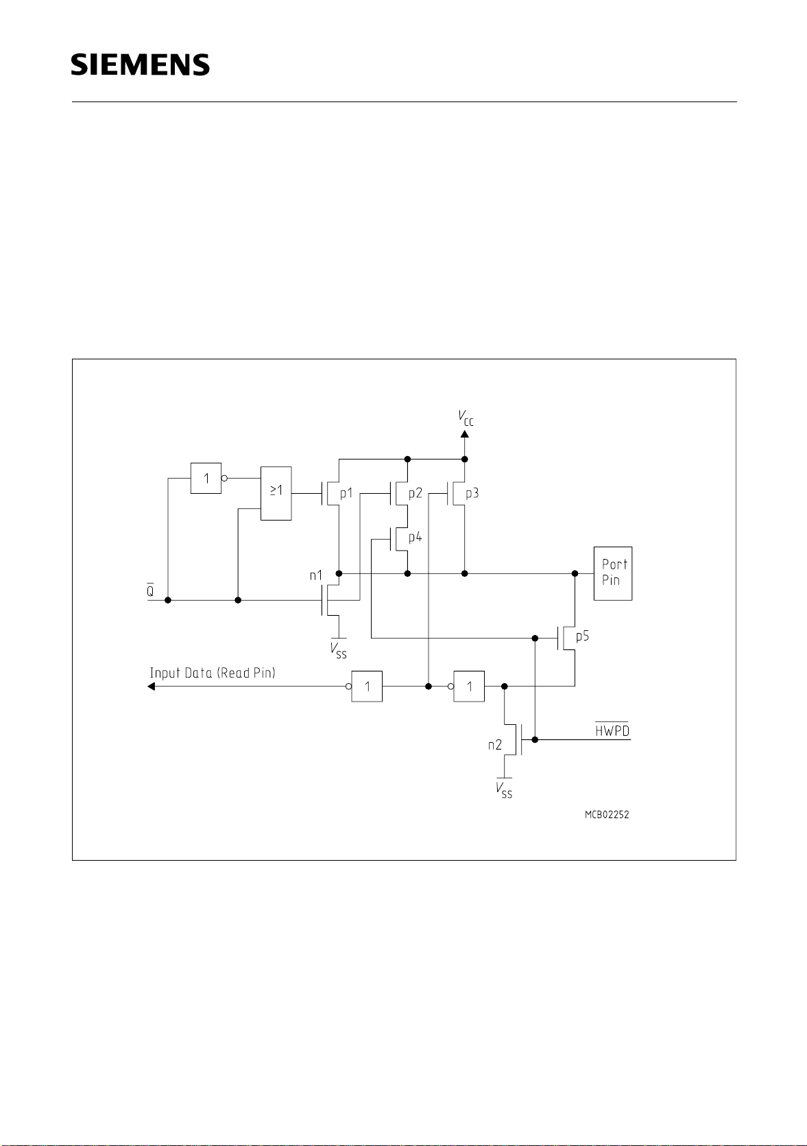
Digital I/O Port Circuitry
To realize the Hardware Power Down Mode with floating Port pins in the SAB 80C515A/83C515A-5
the standard port structure used in the 8051 Family is modified (figure 5-1).
The FETs p4, p5 and n2 are added. During Hardware Power Down this FETs disconnect the port
pins from internal logic.
Figure 5-1
Port Structure
Semiconductor Group 5-1

On-Chip Peripheral Components
P1 and p3 are not active during Hardware Power Down.
P1 is activated only for two oscillator periods i f a 0-to-1 transition is programmed to the port pin (n ot
possible during HWPD).
P3 is turned off during reset state (also HWPD).
For detailed description of the port structure please refer to the SAB 80C515/80C535 User’s
Manual.
Semiconductor Group 5-2

On-Chip Peripheral Components
5.1 10-Bit A/D-Converter
In the SAB 80C515A a new high performance/high speed 8-channel 10-bit A/D-Converter is
implemented. Its successive approximation technique provides 7 µs conversion time
(
f
= 16 MHz). The conversion principle is upward compatible to the one used in the SAB 80C515.
OSC
The major components are shown in figure 5-1.
The comparator is a fully differential comparator f or a high power supply rejection ratio and very low
offset voltages. The capacitor network is binary weighted providing 10-bit resolution.
T
The table below shows the sample time
on
f
and the selected prescaler (see also Bit ADCL in SFR ADCON 1).
OSC
f
[MHz] Prescaler f
osc
12 ÷ 8 1.5 2.67 9.33
and the conversion time TC (including TS), which depend
S
[MHz] TS [µs] TC [µs]
ADC
(incl.
T
)
S
÷ 16 0.75 5.33 18.66
16 ÷ 8 2.0 2.0 7.0
÷ 16 1.0 4.0 14.0
18 ÷ 8 –––
÷ 16 1.125 3.555 12.4
Semiconductor Group 5-3

On-Chip Peripheral Components
Figure 5-2
10-Bit A/D - Co n verter
Semiconductor Group 5-4
Special Function Registers ADCON0, ADCON1
MSB LSB
Bit No.
Addr.
0D8
H
76543210
BD
CLK ADEX BSY ADM MX2 MX1 MX0
MSB LSB
Bit No.
Addr.
0DC
H
76543210
ADCL MX3
These bits are not used in controling A/D converter functions in the 80C515A
On-Chip Peripheral Components
ADCON0
MX2 MX1
MX0
ADCON1
Bit Function
ADEX Internal/external start of conversion.
When set, the external start of conversion by P4.0 / ADST
BSY Busy flag.
This flag indicates whether a conve rsion is in progress (BSY = 1). The flag
is cleared by hardware when the conversion is finished.
ADM A/D Conversion mode.
When set, a continuous conversion is selected.
If cleared, the converter stops after one conversion.
MX2 - MX0 Select 8 input channels of the ADC.
Bits MX0 to MX2 can be written or read either in ADCON0 o r in ADCON1
ADCL ADC Clock.
When set
The reset value of ADCON0 and ADCON1 is 00
f
ADC
= f
/ 16. Has to be set when f
OSC
H
> 16 MHz
OSC
is enabled
Semiconductor Group 5-5

Special Function Register ADDATH, ADDATL
MSB LSB
Bit No.
Addr.
0D9
Bit No.
Addr.
0DA
H
H
76543210
msb
MSB LSB
76543210
lbs
These bits are not used for conversion result
On-Chip Peripheral Components
ADDAT
ADDATL
H
The reset value of ADDATH and ADDATL is 00H.
The registers ADDATH (0D9H) and ADDATL (0DAH) contain the 10-bit conversion result. The data
is read as two 8-bit bytes. Data is presented in left justified format (i.e. the msb is the most left-hand
bit in a 16-bit word). To get a 10-bit conversion result two READ operations are required. Otherwise
ADDATH contains the 8-bit conversion result.
Semiconductor Group 5-6
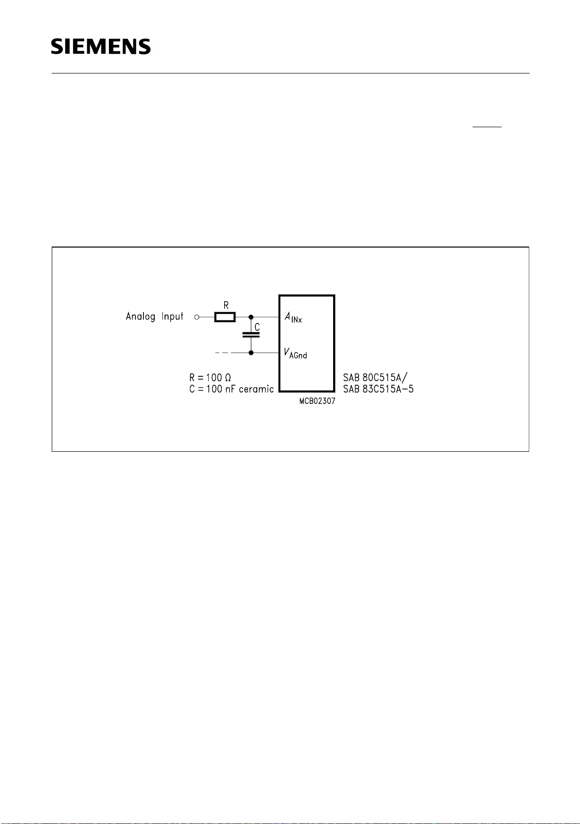
A/D Converter Timing
On-Chip Peripheral Components
After a conversion has been started (by a write to ADDATL, external start by P4.0/ADST
continuous mode) the analog input voltage is sampled for 4 clock cycles. The analog source must
be capable of charging the c apacitor netwo rk of appr. 50 pF to full ac curacy in this time. During this
period the converter is susceptable to spikes and noise at the analo g input, which may cause wrong
codes at the digital outputs. Therefore RC-filteri ng at the analog inputs i s recommended (s ee figure
below).
Conversion of the sampled analog voltage takes place between the 4th an 14th clock cycle.
or in
Figure 5-3
Recommended RC-Filtering at the Analog Inputs
Semiconductor Group 5-7
On-Chip Peripheral Components
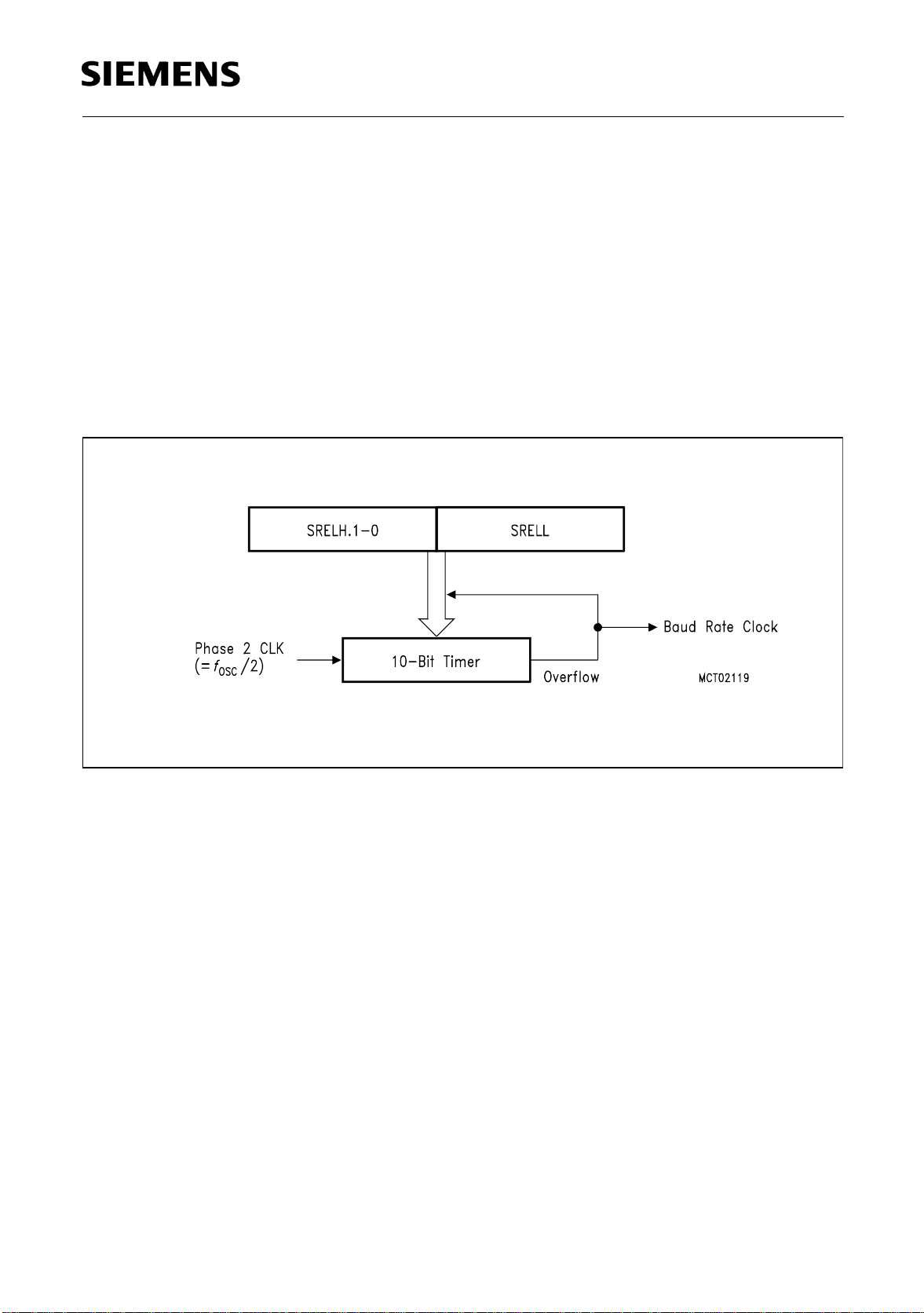
5.2 New Baud Rate Generator for Serial Channel
The Serial Channel has a new baud rate generator which provides greater flexibility and better
resolution. It substitutes the 80C515’s baud rate generator at the Serial Channel which provides
only 4.8 kBaud or 9.6 kBaud at 12 MHz crystal frequency. Since the new generator offers greater
flexibility it is often possible to use it instead of Timer1 which is then free for other tasks.
Figure 5-3 shows a block diagram of the new baud rate generator for the Serial Channel. It consists
of a free running 10-bit timer with
automatic reload from the registers SRELL (address AAH) and SRELH (address BAH). The lower
8 bits of the timer are reloaded from SRELL, while the upper two bits are reloaded from bit 0 and 1
of register SRELH. The baud rate timer is reloaded by writing to SRELL.
f
/ 2 input frequency. On overflow of this timer there is an
OSC
Figure 5-4
Baud Rate Generator for the Serial Interface
Semiconductor Group 5-8

Special Function Register S0RELH, S0RELL
MSB LSB
Bit No.
Addr.
0BA
Bit No.
Addr.
0AA
H
H
76543210
MSB LSB
76543210
shaded areas are not used for programming the baudrate timer
On-Chip Peripheral Components
msb
lsb
SRELH
SRELL
Bit Function
SRELH.0-1 Reload value. Upper two bits of the timer reload value.
SRELL.0-7 Reload value. Lower 8 bit of timer reload value.
Reset value of SRELL is 0D9H, SRELH contains XXXX XX11B.
Semiconductor Group 5-9

On-Chip Peripheral Components
Figure 5-5 shows a block diagram of the options available for baud rate generation of Serial
Channel. It is a fully compatible s uperset of the functionali ty of the SAB 80C515. The new baud ra te
generator can be used in modes 1 and 3 of the Serial Channe l. It is activated by setting bit BD
(ADCON.7). This also starts the baud rate timer. When Timer1 shall be used for baud rate
generation, bit BD must be cleared. In any case, bit SMOD (PCON.7) selects an additional divider
by two.
The default values after reset in registers SRELL and SRELH provide a baud rate of 4.8 kBaud (with
SMOD = 0) or 9.6 kBaud (with SMOD = 1) at 12 MHz oscillator frequency. This guarantees ful l
compatibility to the SAB 80C515.
Figure 5-5
Block Diagram of Baud Rate Generation for Serial Interface
If the new baud rate generator is used the baud rate of the Serial Channel in Mode 1 and 3 can be
determined as follows:
SMOD
2
x oscillator frequency
Mode 1, 3 baud rate =
64 x (2
10
– SREL)
; with SREL = SRELH.1 – 0, SRELL.7 – 0
SMOD
2
x f
OSC
SREL = 210 –
64 x baud rate
Semiconductor Group 5-10

On-Chip Peripheral Components
5.3 Fail Save Mechanisms
The SAB 80C515A offers two on-chip peripherals which ensure an automatic ’fail-save’ reaction in
cases where the controller’s hardware fails or the software hangs up:
– Programmable Watchdog Timer (WDT) with variable time-out period from 512 µs to approx.
1.1 seconds at 12 MHz. The SAB 80C515A's WDT is compat ible to the SAB 80C515's WDT,
which is not programmable.
– An Oscillator Watchdog (OWD) which monitors the on-chip oscillator and forces the
microcontroller into the reset state if the on-c hip oscillator fails . This unit is new in with respec t
to the SAB 80C515.
Semiconductor Group 5-11

On-Chip Peripheral Components
5.3.1 Programmable Watchdog Timer
To protect the system against software upset, the user’s program has to clear the watchdog within
a previously programmed time period. If the software fails to do this periodical refresh of the
Watchdog Timer, an internal hardware reset will be initiated. The software can be designed such
that the watchdog times the if the program does not work properly. It also times out if a software
error is based on hardware-related problems.
The Watchdog Timer in the SAB 80C515A is a 15-bit timer, which is incremented by a count rate of
either
arrangement of two prescalers, a divide-by-two and a divide-by-16 prescaler (see figure 5-6). The
latter is enabled by setting bit WDTREL.7.
f
CYCLE
/2 or f
CYCLE
/32 (f
CYCLE
= f
/12). That is, th e machine clock is d ivided by a series of
OSC
Figure 5-6
Block Diagram of the Programmable Watchdog Timer
Semiconductor Group 5-12

On-Chip Peripheral Components
Special Function Register WDTREL (Address 086H)
Bit No.
MSB LSB
76543210
086
H
Watchdog Timer Reload Register
WDTREL
Bit Function
WDTREL.7 Prescaler select bit.
When set, the watchdog timer is clocked through an additional divide-by-16
prescaler (see figure 12).
WDTREL.6
to
WDTREL.0
Seven bit reload value for the high-byte of the watchdog timer.
This value is loaded to the WDT when a refresh is triggered by a consecutive
setting of bits WDT and SWDT.
Reset value of WDTREL is 00H.
Immediately after start (see next section for start procedure), the Watchdog Timer is initialized to
the reload value programmed to WDTREL.0-WDTREL.6. After an external HW reset (or power-on
reset, or HW Power Down) register WDTREL is cleared to 00H. The lower seven bits of WDTREL
can be loaded by software at any time.
Examples (given for 12 and 18 MHz oscillator frequency):
WDTREL Time-out Period Comments
f
00
H
= 12 MHz f
OSC
65.535 ms 43.690 ms This is the default value and coincides
= 18 MHz
OSC
with the watchdog period of the SAB
80C515
80
7F
H
H
1.1 s 0.73 s maximum time period
512 µs 341 µs minimum time period
Semiconductor Group 5-13

Starting the Watchdog Timer
On-Chip Peripheral Components
There are two ways to start the Watchdog Timer depending on the level applied to the pin PE
(Power Down Modes enable # / Start Watchdog Timer; pin 4). This pin serves two functions (new
for the SAB 80C515A), because it is also used for disabling the software initia ted power saving
modes. For details concerning software initiated power saving modes see User’s Manual
SAB 80C515.
Automatic Start of the Watchdog Timer
The automatic start of the Watchdog Timer directly after an external reset or a Hardware Power
Down (HWPD
pin 4 (PE
mode) are disabled and cannot be started by software. If pin PE
pull-up transistor ensures the automatic start of the Watchdog Timer.
The self-start of the Watchdog Timer by a pin option has been i mplemented to p rovide high system
security in electrically noisy environments.
Note:
The automatic start of the Watchdog Timer is only performed if PE
RESET
not start the Watchdog Timer.
or HWPD is active. A positive transition at these pins during normal program execution will
; PLCC68 pin 60, new for SAB 80C515A) is a hardware start initialized by strapping
/SWD) to VCC. In this case the power saving modes (Software power-down mode and idle
/SWD is left unconnected, a weak
/SWD is held at high level while
/SWD
Furthermore, when using the hardware start, the Watchdo g Timer starts running with its default
time-out period. The value in the reload regis ter WDTREL, howe ver can be overwritten at any time
to set any time-out period desired.
Software Start of the Watchdog Timer
The Watchdog Timer can also be started by software. This method is compatible to the start
procedure in the SAB 80C515. Setting of bit SWDT in SFR IEN1 starts the Watchdog Timer. Using
the software start, the time-out period can be programmed before Watchdog Timer starts running.
Note that once s tarted the Watchdog Time r cannot be stopped by any thing but an external
hardware reset at pin 10 (RESET
at pin 60 (HWPD
, independently of level at PE/SWD).
) with a low level on pin 4 (PE/SWD) or a hardware power down
Semiconductor Group 5-14

On-Chip Peripheral Components
Refreshing the Watchdog Timer
At the same time the Watchdog Timer is started, the 7-bit register WDTH is preset by the contents
of WDTREL.0 to WDTREL.6. Once started the Watchdog Timer cannot be stop ped by software but
can be refreshed to the reload value only by first s etting bit WDT (IEN0.6) and by the next instruction
setting SWDT (IEN1.6). Bit WDT will automatically be cleared during the second machine cycle
after having been set
minimize the chance of an unintentional reset of the watchdog unit.
The reload register WDTREL can be written at any time, as already mentioned. Therefore, a
periodical refresh of WDTREL can be added to the above mentioned starting procedure of the
Watchdog Timer. Thus a wrong reload value caused by a possible distortion during the write
operation to WDTREL can be corrected by software.
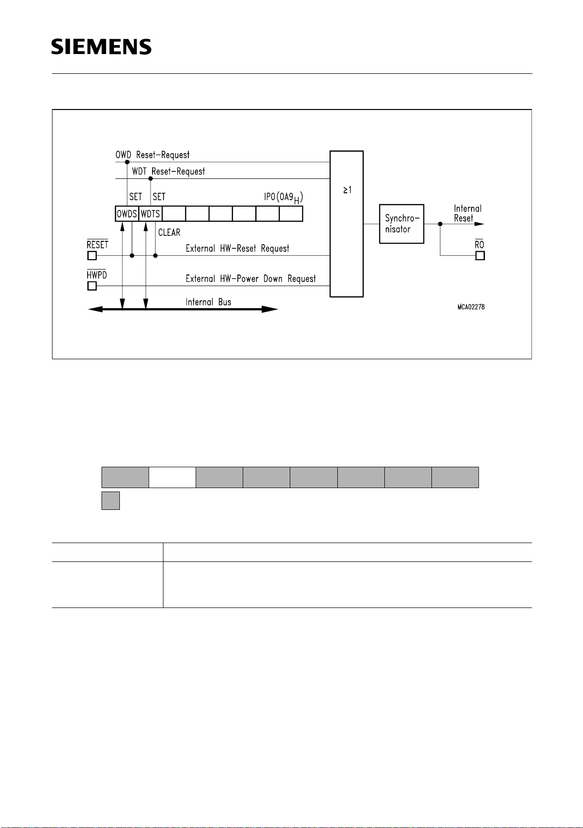
Watchdog Reset and Watchdog Status Flag (WDTS)
If the software fails to clear the watchdog in time, an internally generated watchdog reset i s entered
at the counter state 7FFCH. The duration of the reset signal then depends on the prescaler
selection (either 8 or 128 cycles). This internal reset differs from an external one in so far as the
Watchdog Timer is not disabled and bit WDTS is set. Figure 5-6 shows a block diagram of all reset
requests in the SAB 80C515A and the function of the watchdog status flag. The WDTS is a fl ip-flop,
which is set b y a Watchdog Time r reset and can b e cleared by an ex ternal hardwa re reset. Bit
WDTS allows the software to examine from which source the reset was activated. The bit WDTS
can also be cleared by software.
1)
. This double-instruction refresh of the Watchdog Timer is implemented to
1)
(SETB - Instructions have to be used)
Semiconductor Group 5-15
On-Chip Peripheral Components
Figure 5-7
Watchdog Status Flags and Reset Requests
Special Function Register IP0 (Address 0A9H)
Bit No.
086
Bit Function
WDTS Watchdog timer status flag.
Reset value of IP0 is 00H.
MSB LSB
76543210
OWDS WDTS IP0.5 IP0.4 IP0.3 IP0.2 IP0.1 IP0.0
H
These bits are not used for Watchdog Timer
Set by hardware e when a Watchdog Timer reset occurred . Can be cleared
and set by software.
IPO
Semiconductor Group 5-16

On-Chip Peripheral Components
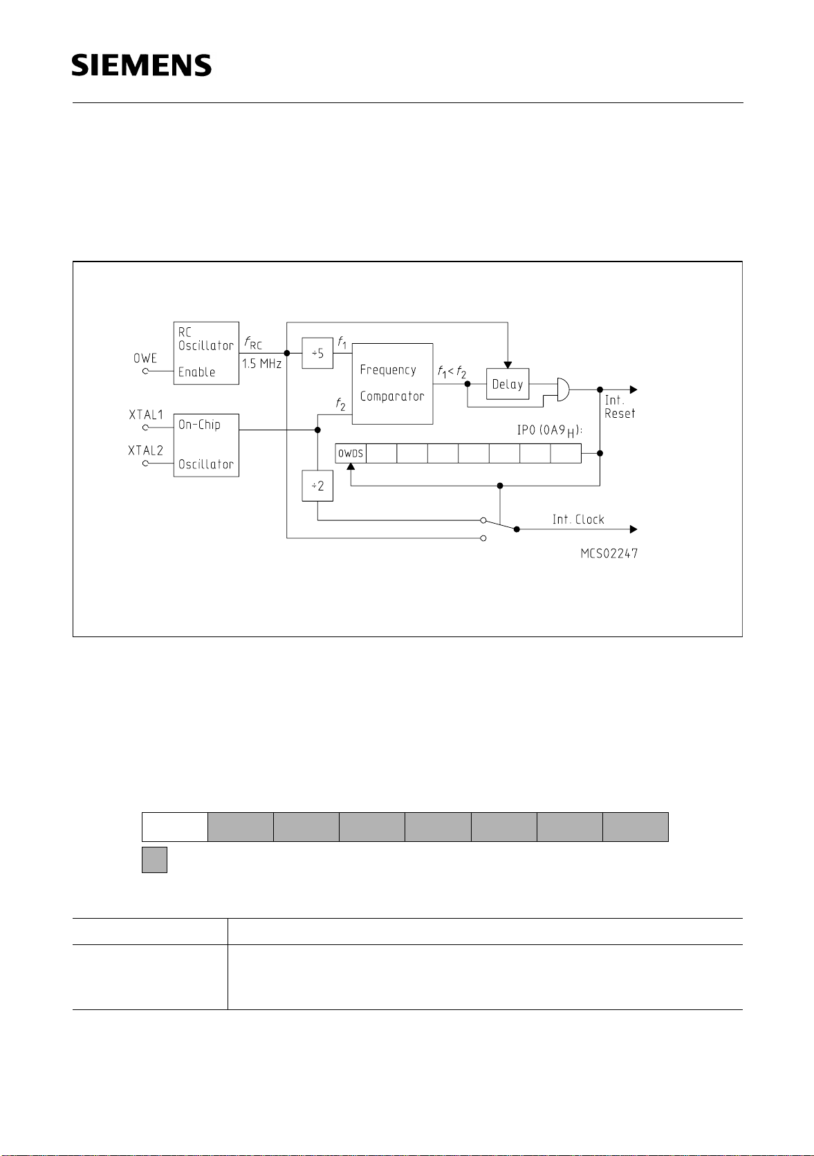
5.3.2 Oscillator Watchdog Unit
The unit serves three functions:
– Monitoring of the on-chip oscillator’s function.
The watchdog supervises the on-chip oscillato r's frequency; if it is lower than the frequency of
the auxiliary RC oscillator in the watchdog unit, the internal clock is supplied by the RC
oscillator and the device is brought into reset; if the failure condition disappears (i.e. the onchip oscillator has a higher frequency than the RC oscillator), the part executes a final reset
phase of appr. 0.5 ms in order to allow the oscillator to stabilize; then the oscillator watchdog
reset is released and the part starts program execution again.
– Restart from the Hardware Power Down Mode.
If the Hardware Power Down Mode is terminated the oscillator watchdog has to control the
correct start-up of the on-chip oscillator and to restart the program. The oscillator watchdog
function is only part of the complete Hardware Power Down sequence; however, the
watchdog works identically to the monitoring function. The Hardware Power Down Mode is
discussed in detail in section 4.1, 4.2
– Fast internal reset after power-on.
In this function the oscillator watchdog unit provides a clock supply for the reset before the onchip oscillator has started. In this case the osc illator watchdog unit also works identically to the
monitoring function. The power-on is described in section 4.3.
Note:
The oscillator watchdog unit is always enabled.
Semiconductor Group 5-17
On-Chip Peripheral Components
Detailed Description of the Oscillator Watchdog Unit
Figure 5-8 shows the block diagram of the oscillator watchdog unit. It consists of an internal RC
oscillator which provides the reference frequency for the comparison with the frequency of the onchip oscillator.
Figure 5-8
Oscillator Watchdog Unit
Special Function Register IP0 (Address 0A9H)
Bit No.
086
Bit Function
OWDS Oscillator watchdog timer status flag.
Reset value of IP0 is 00H.
MSB LSB
76543210
OWDS WDTS IP0.5 IP0.4 IP0.3 IP0.2 IP0.1 IP0.0
H
These bits are not used for Watchdog Timer
Set by hardware when an oscillator watchdog reset occurred. Can be
cleared and set by software.
IPO
Semiconductor Group 5-18

On-Chip Peripheral Components
The frequency coming from the RC oscillat or is divided by 5 and compared to t he on-chip oscillator’ s
frequency. If the frequency coming from the on-chip oscillator is found lower than the frequency
derived from the RC oscillator the watchdog detects a failure condition (t he oscillation at the on-chip
oscillator could stop because of cr ystal damage etc.). In this cas e it switches the input of the internal
clock system to the output of the RC os cillator. This m eans that the part is being clocke d even if the
on-chip oscillator has stopped or has not yet started. At the same time the watchdog activates the
internal reset in order to bring the part in its defined reset state. The reset is performed because
clock is available from the RC oscillator. This internal watchdog reset has the same effects as an
externally applied rese t signal with the following exception s: The Watchdog Timer Status flag
WDTS (IP0.6) is not reset; (the Watchdog Timer however is stopped) and bit OWDS is set. This
allows the software to examine error conditions detected by the Watc hdog Timer even if meanwhile
an oscillator failure occurred.
The oscillator watchdog is able to detect a recovery of the on-chip oscillator after a failure. If the
frequency derived from the on-chip oscillator i s again high er than the referen ce the watchdog starts
a final reset sequence which takes typ. 1 ms. Within that time the clock is still supplied by the RC
oscillator and the part is held in reset. This allows a reliable stabilization of the on chip oscillator.
After that, the watchdog toggles the clock supply back to the on-chip oscillator and releases the
reset request. If no external reset is applied in this moment the part will start program execution. If
an external reset is active, however, the device will keep the reset state until also the external reset
request disappears.
Furthermore, the status flag OWDS (IP0.7) is set if the oscillator watchdog was active. The status
flag can be evaluated by software to detect that a reset was caused by the oscillator watchdog. The
flag OWDS can be set or cleared by software. An external reset request, however, also resets
OWDS (and WDTS).
Semiconductor Group 5-19

High-Performance SAB 80C515A / 83C515A-5
8-Bit CMOS Single-Chip Microcontroller
Preliminary
SAB 83C515A-5 Microcontroller with factory mask-programmable ROM
SAB 80C515A Microcontroller for external ROM
●
SAB 80C515A / 83C515A-5, up to 18 MHz operation frequency
32 K
●
●
256
●
Additional 1 K
Superset of SAB 80C51 architecture:
●
1
666 ns instruction cycle time at 18 MHz
256 directly addressable bits
Boolean processor
64 Kbyte external data and program memory addressing
Three 16-bit timer/counters
●
●
Versatile "fail-safe" provisions
●
Twelve interrupt vectors, four priority levels selectable
Genuine 10-bit A/D converter with 8 multiplexed inputs
●
●
Full duplex serial interface with programmable Baudrate-Generator
●
Functionally compatible with SAB 80C515
Extended power saving mode
●
●
Fast Power-On Reset
●
Seven ports: 48 I/O lines, 8 input lines
Two temperature ranges available:
●
0 to 70 ° C (T1)
– 40 to 85 ° C (T3)
Plastic packages: P-LCC-68 and P-MQFP-80
●
8 ROM (SAB 83C515A-5 only, ROM-Protection available)
×
×
8 on-chip RAM
×
8 on-chip RAM (XRAM)
µ
s instruction cycle time at 12 MHz
The SAB 80C515A/83C515A-5 is a high-end member of the Siemens SAB 8051
microcontroller family. It is designed in Siemens ACMOS technology and based on the
SAB 8051 architecture. ACMOS is a technology which combines high-speed and density
characteristics with low-power consumption or dissipation.
While maintaining all the SAB 80C515 features and operating characteristics the
SAB 80C515A/83C515A-5 contains more on-chip RAM/ROM. Furthermore a new 10-bit A/DConverter is implemented as well as extended security mechanisms. The SAB 80C515A is
identical with the SAB 83C515A-5 except that it lacks the on-chip program memory. The
SAB 80C515A / 83C515A-5 is supplied in a 68-pin plastic leaded chip carrier package
(P-LCC- 68) and in a 80-pin plastic metric quad flat package (P-MQFP-80).
Versions for extended temperature range – 40 to + 110 ∞ C are available on request.
p
-
SAB 80C515A/83C515A-5
Ordering Information
Type Ordering
Code
Package Description
8-Bit CMOS microcontroller
SAB 80C515A-N18 Q67120-C0581 P-LCC-68 for external memory, 18 MHz
SAB 83C515A-5N18 Q67120-DXXXX P-LCC-68 with mask-programmable ROM,
18 MHz
SAB 80C515A-N18-T3 Q67120-C0784 P-LCC-68 for external memory, 18 MHz
ext. temperature − 40 to + 85 ° C
SAB 83C515A-5N18-T3 Q67120-DXXXX P-LCC-68 with mask-programmable ROM,
18 MHz
ext. temperature − 40 to + 85 ° C
SAB 80C515A-M18-T3 Q67120-C0851 P-MQFP-80 for external memory, 18 MHz
ext. temperature − 40 to + 85 ° C
SAB 83C515A-5M18-T3 Q67120-DXXXX P-MQFP-80 with mask-programmable ROM,
18 MHz
ext. temperature − 40 to + 85 ° C
Notes
:
Versions for extended temperature range − 40 to + 110
The ordering number of ROM types (DXXXX extension) is defined after program release
(verification) of the customer.
C on request.
°
Semiconductor Group 6-2
SAB 80C515A/83C515A-5
Logic Symbol
Semiconductor Group 6-3
SAB 80C515A/83C515A-5
The pin functions of the SAB 80C515A are identical with those of the SAB 80C515 with
following exception:
Pin SAB 80C515A SAB 80C515
68
1
4
HWPD
P0.4/ADST
PE/SWD
V
CC
P4.0
PE
Pin Configuration
(P-LCC-68)
Semiconductor Group 6-4

N.C. pins must not be connected.
P0.6 / AD6
SAB 80C515A / 80C515A-5
80
1
5
10
15
20
21 25 30
40
41
35
45
50
55
60
61
657075
P0.7 / AD7
P0.5 / AD5
P0.4 / AD4
P0.2 / AD2
P0.3 / AD3
P0.1 / AD1
P0.0 / AD0
P5.7
N.C.
EA
ALE
PSEN
P2.7 / A15
N.C.
N.C.
P2.6 / A14
P2.5 / A13
P2.4 / A12
P2.3 / A11
VAREF
N.C.
VAGND
P6.7 / AIN7
P6.5 / AIN5
P6.6 / AIN6
P6.4 / AIN4
P6.3 / AIN3
RESET
P6.2 / AIN2
P6.0 / AIN0
N.C.
N.C.
P3.1 / TXD0
P6.1 / AIN1
P3.0 / RXD0
P3.2 / INT0
P3.3 / INT1
P3.4 / T0
P3.5 / T1
N.C.
P3.7 / RD
P1.7 / T2
P1.6 / CLKOUT
P1.4 / INT2
P1.5 / T2EX
P1.3 / INT6 / CC3
P1.2 / INT5 / CC2
P3.6 / WR
P1.1 / INT4 / CC1
VCC
VCC
VSS
XTAL2
P1.0 / INT3
/ CC0
VSS
XTAL1
P2.0 / A8
P2.1 / A9
P2.2 / A10
P4.5
P4.6
P4.4
P4.3
P4.2
PE
/ SWD
P4.1
P4.0 / ADST
P4.7
N.C.
HWPD
N.C.
P5.0
P5.2
N.C.
P5.1
P5.3
P5.4
P5.5
P5.6
SAB 80C515A/83C515A-5
Pin Configuration
(P-MQFP-80 )
Semiconductor Group 6-5

Pin Definitions and Functions
SAB 80C515A/83C515A-5
Symbol Pin
P-LCC-68
Pin
P-MQFP-80
P4.0-P4.7 1-3, 5-9 72-74,
76-80
PE
/SWD 4 75 I
Input (I)
Output (O)
I/O
Function
Port 4
is an 8-bit bidirectional I/O port with internal
pull-up resistors. Port 4 pins that have 1’s written to them are pulled high by the internal pullup resistors, and in that state can be used as
inputs. As inputs, port 4 pins being externally
pulled low will source current (
I
, in the DC
IL
characteristics) because of the internal pull-up
resistors.
P4 also contains the external A/D converter
control pin. The output latch corresponding to
a secondary function must be programmed to
a one (1) for that function to operate. The secondary function assigned to port 6:
– ADST
(P4.0): external A/D converter start
pin
Power saving mode enable/Start Watchdog Timer
A low level on this pin allows the software to
enter the power down, idle and slow down
mode. In case the low level is also seen during
reset, the watchdog timer function is off on default.
Use of the software controlled power saving
modes is blocked, when this pin is held on
high level. A high level during reset performs
an automatic start of the watchdog timer immediately after reset.
When left unconnected this pin is pulled high
by a weak internal pull-up resistor.
RESET
V
AREF1
V
AGND
10 1 I
11 3
12 4
Semiconductor Group 6-6
Reset pin
A low level on this pin for the duration of two
machine cycles while the oscillator is running
resets the SAB 80C515A. A small internal
pullup resistor permits power-on reset using
only a capacitor connected to
V
SS
Reference voltage for the A/D converter
Reference ground for the A/D converter

Pin Definitions and Functions (cont’d)
SAB 80C515A/83C515A-5
Symbol Pin
P-LCC-68
Pin
P-MQFP-80
Input (I)
Output (O)
P6.7-P6.0 13-20 5-12 I
P3.0-P3.7 21-28 15-22 I/O
Function
Port 6
is an 8-bit unidirectional input port to the A/
D converter. Port pins can be used for digital
input, if voltage levels simultaneously meet
the specifications high/low input voltages, and
for the eight multiplexed analog inputs.
Port 3
is an 8-bit bidirectional I/O port with internal
pullup resistors. Port 3 pins that have1's
written to them are pulled high by the internal
pullup resistors, and in that state can be used
as inputs. As inputs, port 3 pins being
externally pulled low will source current (
I
, in
IL
the DC characteristics) because of the internal
pullup resistors. Port 3 also contains the
interrupt, timer, serial port and external
memory strobe pins that are used by various
options. The output latch corresponding to a
secondary function must be programmed to a
one (1) for that function to operate. The
secondary functions are assigned to the pins
of port 3, as follows:
–R
×
D (P3.0): serial port’s receiver data
input (asynchronous) or data
input/output (synchronous)
–T
×
D (P3.1): serial port’s transmitter data
output (asynchronous) or
clock output (synchronous)
– INT0
(P3.2): interrupt 0 input/timer 0 gate
control input
– INT1
(P3.3): interrupt 1 input/timer 1 gate
control input
– T0 (P3.4): counter 0 input
– T1 (P3.5): counter 1 input
–WR
(P3.6): the write control signal
latches the data byte from
port 0 into the external data
memory
–RD
(P3.7): the read control signal
enables the external data
memory to port 0
Semiconductor Group 6-7

Pin Definitions and Functions (cont’d)
–
SAB 80C515A/83C515A-5
Symbol Pin
P-LCC-68
P1.7 P1.0
29-36 24-31 I/O
Pin
P-MQFP-80
Input (I)
Output (O)
Function
Port 1
is an 8-bit bidirectional I/O port with internal
pullup resistors. Port 1 pins that have 1's
written to them are pulled high by the internal
pullup resistors, and in that state can be used
as inputs. As inputs, port 1 pins being
externally pulled low will source current (
the DC characteristics) because of the internal
pullup resistors. The port is used for the loworder address byte during program
verification. Port 1 also contains the interrupt,
timer, clock, capture and compare pins that
are used by various options. The output latch
corresponding to a secondary function must
be programmed to a one (1) for that function to
operate (except when used for the compare
functions). The secondary functions are
assigned to the port 1 pins as follows:
– INT3
/CC0 (P1.0): interrupt 3 input /
compare 0 output /
capture 0 input
I
in
IL
XTAL2 39 36
– INT4/CC1 (P1.1): interrupt 4 input /
compare 1 output /
capture 1 input
– INT5/CC2 (P1.2): interrupt 5 input /
compare 2 output /
capture 2 input
– INT6/CC3 (P1.3): interrupt 6 input /
compare 3 output /
capture 3 input
– INT2
– T2EX (P1.5): timer 2 external
– CLKOUT (P1.6): system clock output
– T2 (P1.7): counter 2 input
XTAL2
Input to the inverting oscillator amplifier and
input to the internal clock generator circuits.
(P1.4): interrupt 2 input
reloadtrigger input
Semiconductor Group 6-8

Pin Definitions and Functions (cont’d)
SAB 80C515A/83C515A-5
-
Symbol Pin
P-LCC-68
XTAL1 40 37
P2.0-P2.7 41-48 38-45 I/O
Pin
P-MQFP-80
Input (I)
Output (O)
Function
XTAL1
Output of the inverting oscillator amplifier.
To drive the device from an external clock
source, XTAL2 should be driven, while XTAL1
is left unconnected. There are no requirements on the duty cycle of the external clock
signal, since the input to the internal clokking circuitry is divided down by a divide-bytwo flip-flop. Minimum and maximum high and
low times and rise/fall times specified in the
AC characteristics must be taken into account.
Port 2
is an 8-bit bidirectional I/O port with internal
pullup resistors. Port 2 pins that have 1's
written to them are pulled high by the internal
pullup resistors, and in that state can be used
as inputs. As inputs, port 2 pins being
externally pulled low will source current (
the DC characteristics) because of the internal
pullup resistors.
Port 2 emits the high-order address byte
during fetches from external program memory
and during accesses to external data memory
that use 16-bit addresses (MOVX@DPTR). In
this application it uses strong internal pullup
resistors when issuing 1's. During accesses to
external data memory that use 8-bit
addresses (MOVX@Ri), port 2 issues the
contents of the P2 special function register.
I
in
IL,
PSEN
ALE 50 48 O The
49 47 O The Program Store Enable
output is a control signal that enables the
external program memory to the bus during
external fetch operations. It is activated every
six oscillator periods, except during external
data memory accesses. The signal remains
high during internal program execution.
output is used for latching the address into
external memory during normal operation. It is
activated every six oscillator periods, except
during an external data memory access.
Semiconductor Group 6-9
Address Latch enable

Pin Definitions and Functions (cont’d)
SAB 80C515A/83C515A-5
Symbol Pin
P-LCC-68
Pin
P-MQFP-80
Input (I)
Output (O)
Function
EA 51 49 I External Access Enable
When held high, the SAB 80C515A executes
instructions from the internal ROM as long as
the PC is less than 32768. When held low, the
SAB 80C515A fetches all instructions from
external program memory. For the SAB
80C515A this pin must be tied low.
P0.0-P0.7 52-59 52-59 I/O Port 0
is an 8-bit open-drain bidirectional I/O port.
Port 0 pins that have 1's written to them float,
and in that state can be used as highimpedance inputs.
Port 0 is also the multiplexed low-order
address and data bus during accesses to
external program and data memory. In this
application it uses strong internal pullup
resistors when issuing 1's.
Port 0 also outputs the code bytes during
program verification in the SAB 80C515A.
External pullup resistors are required during
program verification.
P5.7-P5.0 60-67 60-67 I/O Port 5 is an 8-bit bidirectional I/O port with
internal pullup resistors. Port 5 pins that have
1's written to them are pulled high by the
internal pullup resistors, and in that state can
be used as inputs. As inputs, port 5 pins being
externally pulled low will source current
(I
in the DC characteristics) because of the
IL
internal pullup resistors.
HWPD
68 69 I Hardware Power Down
A low level on this pin for the duration of one
machine cycle while the oscillator is running
resets the SAB 80C515A.
A low level for a longer period will force the
part to Power Down Mode with the pins floating. (see table 5)
V
CC
37 32, 33 – Supply voltage
during normal, idle, and power-down operation.
V
SS
N.C. – 2, 13, 14, 23,
38 34, 35 – Ground (0 V)
– Not connected
46, 50, 51,
68, 70, 71
These pins of the P-MQFP-80 package must
not be connected.
Semiconductor Group 6-10

SAB 80C515A/83C515A-5
Figure 1
Block Diagram
Semiconductor Group 6-11
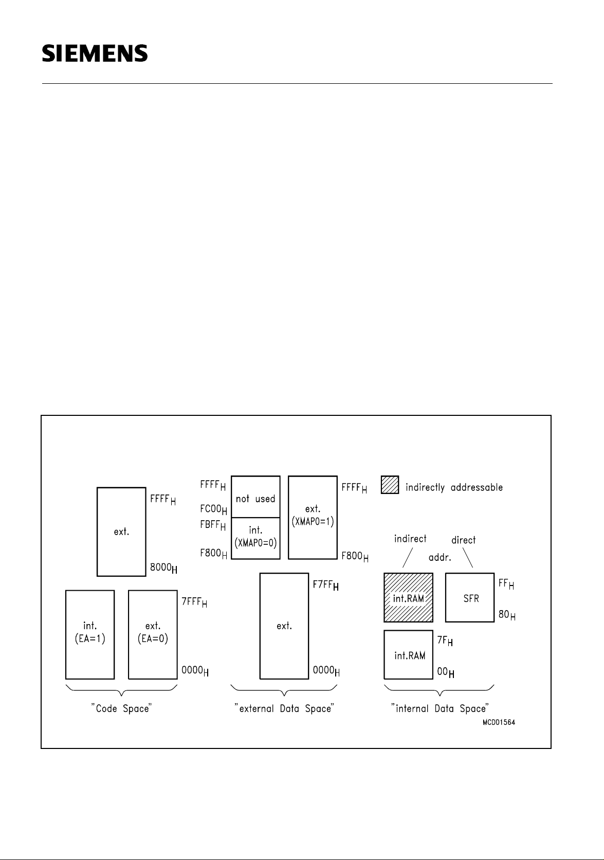
SAB 80C515A/83C515A-5
Functional Description
The SAB 80C515A is based on 8051 architecture. It is a fully compatible member of the
Siemens SAB 8051/80C51 microcontroller family being an significantly enhanced
SAB 80C515. The SAB 80C515A is therefore code compatible with the SAB 80C515.
Having an 8-bit CPU with extensive facilities for bit-handling and binary BCD arithmetics the
SAB 80C515A is optimized for control applications. With a 18 MHz crystal, 58 % of the
instructions are executed in 666.67 ns.
While maintaining all architectural and operational characteristics of the SAB 80C515 the SAB
80C515A incorporates more on-chip RAM. A new 10-bit A/D-Converter is implemented as well
as an oscillator watchdog unit. Also the maximum operating frequency of 18 MHz is higher than
at the SAB 80C515.
With exception of the ROM sizes both parts are identical. Therefore the therm SAB 80C515A
refers to both versions within this specification unless otherwise noted.
Memory Organisation
According to the SAB 8051 architecture, the SAB 80C515A has separate address spaces for
program and data memory. Figure 2 illustrates the mapping of address spaces.
Figure 2
Memory Map
Semiconductor Group 6-12

SAB 80C515A/83C515A-5
Program Memory ('Code Space')
The SAB 83C515A-5 has 32 Kbyte of on-chip ROM, while the SAB 80C515A has no internal
ROM. The program memory can externally be expanded up to 64 Kbyte. Pin EA
whether program fetches below address 8000
are done from internal or external memory.
H
As a new feature the SAB 83C515A-5 offers the possibility of protecting the internal ROM
against unauthorized access. This protection is implemented in the ROM-Mask. Therefore, the
decision ROM-Protection 'yes' or 'no' has to be made when delivering the ROM-Code. Once
enabled, there is no way of disabling the ROM-Protection.
Effect: The access to internal ROM done by an externally fetched MOVC instruction is
disabled. Nevertheless, an access from internal ROM to external ROM is possible.
To verify the read protected ROM-Code a special ROM-Verify-Mode is implemented. This
mode also can be used to verify unprotected internal ROM.
determines
ROM -Protection ROM-Verification Mode
Restrictions
(see 'AC Characteristics')
no ROM-Verification Mode 1
–
(standard 8051 Verification Mode)
ROM-Verification Mode 2
yes ROM-Verification Mode 2 – standard 8051
Verification Mode is
disabled
– externally applied MOVC
accessing internal ROM
is disabled
Semiconductor Group 6-13

SAB 80C515A/83C515A-5
Data Memory ('Data Space')
The data memory space consists of an internal and an external memory space.The
SAB 80C515A contains another 1 Kbyte on On-Chip RAM additional to the 256-bytes internal
RAM of the base type SAB 80C515. This RAM is called XRAM ('extended RAM') in this
document.
External Data Memory
Up to 64 Kbyte external data memory can be addressed by instructions that use 8-bit or 16-bit
indirect addressing. For 8-bit addressing MOVX instructions in combination with registers R0
and R1 can be used. A 16-bit external memory addressing is supported by a 16-bit datapointer.
Registers XPAGE and SYSCON are controlling whether data fetches at addresses F800
FBFF
are done from internal XRAM or from external data memory.
H
Internal Data Memory
H
to
The internal data memory is divided into four physically distinct blocks:
– the lower 128 bytes of RAM including four register banks containing eight
registers each
– the upper 128 byte of RAM
– the 128 byte special function register area.
– a 1 K
chip at the address range from F800
× 8 area which is accessed like external RAM (MOVX-instructions), implemented on
to FBFFH. Special Function Register SYSCON
H
controls whether data is read from or written to XRAM or external RAM.
A map of the internal data memory is shown in figure 2. The overlapping address spaces of the
standard internal data memory (256 byte) are accessed by different addressing modes (see
User's Manual SAB 80C515). The stack can be located anywhere in the internal data memory.
Architecture of the XRAM
The contents of the XRAM is not affected by a reset or HW Power Down. After power-up the
contents is undefined, while it remains unchanged during and after a reset or HW Power Down
if the power supply is not turned off.
The additional On-Chip RAM is logically located in the "external data memory" range at the
upper end of the 64 Kbyte address range (F800
enabled the address range F800
to FFFFH is occupied. This is done to assure software
H
-FBFFH). Nevertheless when XRAM is
H
compatibility to SAB 80C517A. It is possible to enable and disable (only by reset) the XRAM. If
it is disabled the device shows the same behaviour as the parts without XRAM, i.e. all MOVX
accesses use the external bus to physically external data memory.
Semiconductor Group 6-14

SAB 80C515A/83C515A-5
Accesses to XRAM
Because the XRAM is used in the same way as external data memory the same instruction
types must be used for accessing the XRAM.
Note:
If a reset occurs during a write operation to XRAM, the effect on XRAM depends on the
cycle which the reset is detected at (MOVX is a 2-cycle instruction):
Reset detection at cycle 1: The new value will not be written to XRAM. The old value
is not affected.
Reset detection at cycle 2: The old value in XRAM is overwritten by the new value.
Accesses to XRAM using the DPTR
There are a Read and a Write instruction from and to XRAM which use one of the 16-bit DPTR
for indirect addressing. The instructions are:
MOVX A, @DPTR (Read)
MOVX @DPTR, A (Write)
Normally the use of these instructions would use a physically external memory. However, in the
SAB 80C515A the XRAM is accessed if it is enabled and if the DPTR points to the XRAM
address space (DPTR ≥ F800
Accesses to XRAM using the Registers R0/R1
The 8051 architecture provides also instructions for accesses to external data memory range
which use only an 8-bit address (indirect addressing with registers R0 or R1). The instructions
are:
).
H
MOVX A, @Ri (Read)
MOVX @Ri, A (Write)
In application systems, either a real 8-bit bus (with 8-bit address) is used or Port 2 serves as
page register which selects pages of 256-byte. However, the distinction, whether Port 2 is
used as general purpose I/O or as "page address" is made by the external system design. From
the device’s point of view it cannot be decided whether the Port 2 data is used externally as
address or as I/O data!
Hence, a special page register is implemented into the SAB 80C515A to provide the possibility
of accessing the XRAM also with the MOVX @Ri instructions, i.e. XPAGE serves the same
function for the XRAM as Port 2 for external data memory.
Semiconductor Group 6-15

Special Function Register XPAGE
SAB 80C515A/83C515A-5
Addr. 91
H
XPAGE
The reset value of XPAGE is 00H.
XPAGE can be set and read by software.
The register XPAGE provides the upper address byte for accesses to XRAM with MOVX @Ri
instructions. If the address formed from XPAGE and Ri is less than the XRAM address range,
then an external access is performed. For the SAB 80C515A the contents of XPAGE must be
greater or equal than F8
in order to use the XRAM. Of course, the XRAM must be enabled if
H
it shall be used with MOVX @Ri instructions.
Thus, the register XPAGE is used for addressing of the XRAM; additionally its contents are
used for generating the internal XRAM select. If the contents of XPAGE is less than the XRAM
address range then an external bus access is performed where the upper address byte is
provided by P2 and not by XPAGE!
Therefore, the software has to distinguish two cases, if the MOVX @Ri instructions with paging
shall be used:
a) Access to XRAM: The upper address byte must be written to XPAGE or P2;
both writes selects the XRAM address range.
b) Access to external memory: The upper address byte must be written to P2; XPAGE will
be loaded with the same address in order to deselect the
XRAM.
Semiconductor Group 6-16
SAB 80C515A/83C515A-5
Control of XRAM in the SAB 80C515A
There are two control bits in register SYSCON which control the use and the bus operation
during accesses to the additional On-Chip RAM (XRAM).
Special Function Register SYSCON
Addr. 0B1
H
XMAP1 XMAP0 SYSCON
Bit Function
XMAP0 Global enable/disable bit for XRAM memory.
XMAP0 =0: The access to XRAM (= On-Chip XDATA memory) is en-
abled.
XMAP0 = 1: The access to XRAM is disabled. All MOVX accesses are
performed by the external bus (reset state).
XMAP1 Control bit for / RD/WR
signals during accesses to XRAM; this bit has no
effect if XRAM is disabled (XMAP0 = 1) or if addresses exceeding the
XRAM address range are used for MOVX accesses.
XMAP1 = 0: The signals RD
and WR are not activated during accesses
to XRAM.
XMAP1 = 1: The signals RD
and WR are activated during accesses to
XRAM.
Reset value of SYSCON is XXXX XX01B.
The control bit XMAP0 is a global enable/disable bit for the additional On-Chip RAM (XRAM).
If this bit is set, the XRAM is disabled, all MOVX accesses use external memory via the external
bus. In this case the SAB 80C515A does not use the additional On-Chip RAM and is compatible
with the types without XRAM.
Semiconductor Group 6-17

SAB 80C515A/83C515A-5
XMAP0 is hardware protected by an unsymmetric latch. An unintentional disabling of XRAM
could be dangerous since indeterminate values would be read from external bus. To avoid this
the XMAP-bit is forced to '1' only by reset. Additionally, during reset an internal capacitor is
loaded. So after reset state XRAM is disabled. Because of the load time of the capacitor
XMAP0-bit once written to '0' (that is, discharging capacitor) cannot be set to '1' again by
software. On the other hand any distortion (software hang up, noise, ...) is not able to load this
capacitor, too. That is, the stable status is XRAM enabled. The only way to disable XRAM after
it was enabled is a reset.
The clear instruction for XMAP0 should be integrated in the program initialization routine before
XRAM is used. In extremely noisy systems the user may have redundant clear instructions.
The control bit XMAP1 is relevant only if the XRAM is accessed. In this case the external RD
and WR
debug purposes it might be useful to have these signals and the addresses at Ports 0.2
available. This is performed if XMAP1 is set.
The behaviour of Port 0 and P2 during a MOVX access depends on the control bits in register
SYSCON and on the state of pin EA
the following characteristics:
a) Use of P0 and P2 pins during the MOVX access.
Bus: The pins work as external address/data bus. If (internal) XRAM
I/0: The pins work as Input/Output lines under control of their latch.
b) Activation of the RD
c) Use of internal or external XDATA memory.
The shaded areas describe the standard operation as each 80C51 device without on-chip
XRAM behaves.
signals at P3.6 and P3.7 are not activated during the access, if XMAP1 is cleared. For
. The table 1 lists the various operating conditions. It shows
is accessed, the data written to the XRAM can be seen on the bus in
debug mode.
and WR pin during the access.
Semiconductor Group 6-18
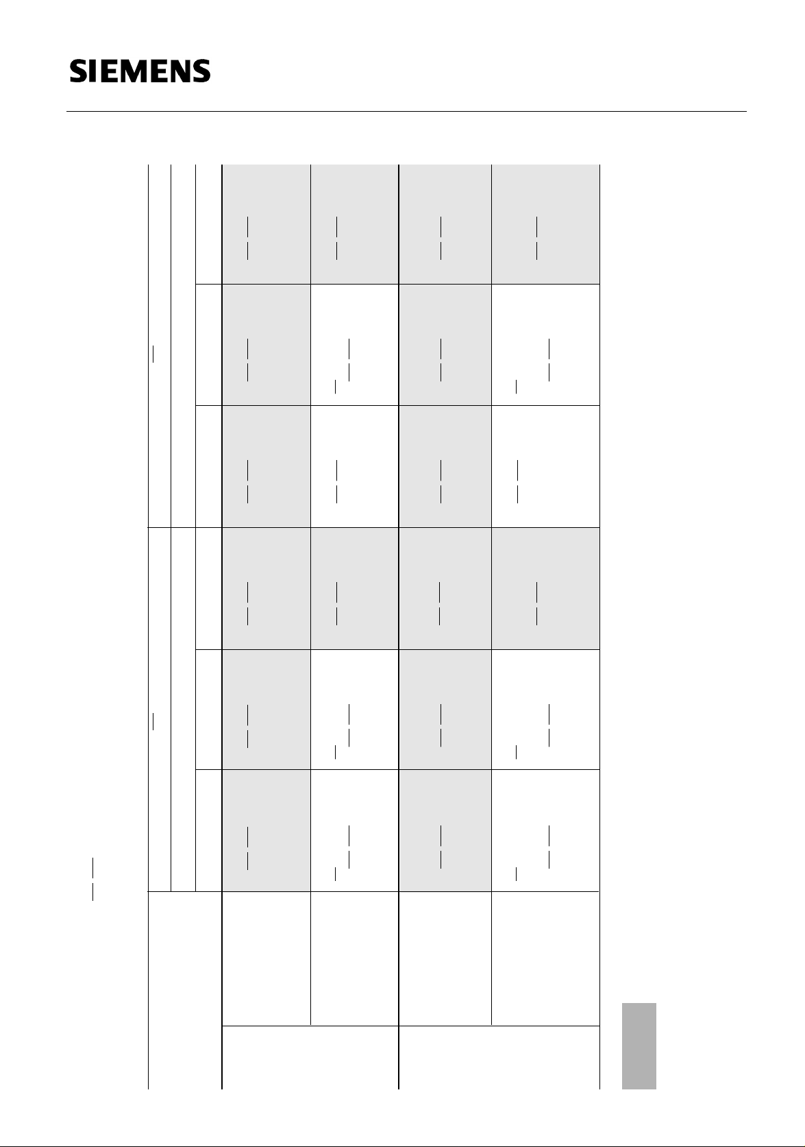
EA = 1
XMAP1, XMAP0
➝Bus
RD/WR active
c) ext. memory is
a) P0/P2
b)
➝Bus
RD/WR active
c) ext. memory is
a) P0/P2
b)
used
used
RD/WR active
c) ext. memory is
a) P0/P2➝Bus
b)
a) P0/P2➝BUS
(WR -Data only)
b) RD/WR active
➝Bus
➝I/0
a) P0
P2
RD/WR active
b)
used
➝Bus
➝I/0
c) XRAM is used
P2
a) P0
RD/WR active
b)
SAB 80C515A/83C515A-5
➝Bus
➝I/0
a) P0
P2
a) P0➝BUS
(WR -Data only)
RD/WR active
b)
P2➝I/0
c) ext. memory is
used
c) ext. memory is
used
c) ext. memory is
used
RD/WR active
c) XRAM is used
b)
➝Bus
00 10 X1
RD/WR active
c) ext. memory is
a) P0/P2
b)
➝Bus
RD/WR active
c) ext. memory is
b)
a) P0/P2
➝Bus
EA = 0
XMAP1, XMAP0
00 10 X1
/WR active
a) P0/P2
b) RD
c) ext. memory is
➝Bus
/WR active
a) P0/P2
c) ext. memory is
b) RD
RD/WR during MOVX accesses
used
used
used
used
RD/WR inactive
c) XRAM is used
a) P0/P2➝I/0
b)
➝Bus
RD/WR active
c) ext. memory is
b)
a) P0/P2
a) P0/P2➝BUS
(WR -Data only)
b) RD/WR active
a) P0/P2➝BUS
(WR -Data only)
b) RD/WR inactive
➝Bus
➝I/0
RD/WR active
a) P0
P2
b)
➝Bus
➝I/0
a) P0
P2
RD/WR active
b)
used
➝Bus
➝I/0
c) XRAM is used
c) XRAM is used
P2
a) P0
➝I/0
a) P0➝Bus
P2
RD/WR active
b)
RD/WR active
b)
RD/WR inactive
c) ext. memory is
used
c) XRAM is used
a) P0/P2➝I/0
b)
➝Bus
➝I/0
c) ext. memory is
used
c) ext. memory is
used
c) ext. memory is
used
a) P0
P2
a) P0/P2➝BUS
(WR -Data only)
a) P0/P2➝BUS
(WR -Data only)
RD/WR active
b)
P2➝I/0
P2➝I/0
c) ext. memory is
used
RD/WR active
c) XRAM is used
b)
RD/WR inactive
b)
c) XRAM is used
address
range
DPTR ≥ XRAM
DPTR < XRAM
Table 1:
Behaviour of P0/P2 and
address
range
MOVX
@DPTR
Semiconductor Group 6-19
addr.
range
XPAGE < XRAM
page
@Ri
MOVX
addr.
XPAGE ≥ XRAM
range
modes compatible to 8051 - family
page

SAB 80C515A/83C515A-5
Special Function Registers
All registers, except the program counter and the four general purpose register banks, reside
in the special function register area. The special function registers include arithmetic registers,
pointers, and registers that provide an interface between the CPU and the on-chip peripherals.
There are also 128 directly addressable bits within the SFR area. All special function registers
are listed in table 2 and table 3.
In table 2 they are organized in numeric order of their addresses. In table 3 they are organized
in groups which refer to the functional blocks of the SAB 80C515A.
Table 2
Special Function Register
Address Register Contents
Address Register Contents
after Reset
1)
80
H
81
H
82
H
83
H
84
H
85
H
86
H
87
H
88
H
89
H
8A
H
8B
H
8C
H
8D
H
8E
H
8F
H
90
H
91
H
92
H
93
H
94
H
95
H
96
H
97
H
1)
Bit-addressable special function registers
2)
X means that the value is indeterminate and the location is reserved
P0
SP
DPL
DPH
(WDTL)
(WDTH)
WDTREL
PCON
TCON
1)
TMOD
TL0
TL1
TH0
TH1
reserved
reserved
1)
P1
XPAGE
reserved
reserved
reserved
reserved
reserved
reserved
0FF
07
00
00
00
00
00
00
00
00
00
00
XX
XX
0FF
XX
XX
XX
XX
XX
XX
XX
H
H
H
H
H
H
H
H
H
H
H
H
2)
H
2)
H
H
2)
H
2)
H
2)
H
2)
H
2)
H
2)
H
2)
H
98
99
9A
9B
9C
9D
9E
9F
A0
A1
A2
A3
A4
A5
A6
A7
A8
A9
AA
AB
AC
AD
AE
AF
H
H
H
H
H
H
H
H
H
H
H
H
H
H
H
H
H
H
H
H
H
H
H
H
S0CON
SBUF
reserved
reserved
reserved
reserved
reserved
reserved
1)
P2
reserved
reserved
reserved
reserved
reserved
reserved
reserved
IEN0
1)
IP0
SRELL
reserved
reserved
reserved
reserved
reserved
after Reset
1)
00
H
XXH
XX
H
XX
H
XX
H
XX
H
XX
H
XX
H
0FF
H
XX
H
XX
H
XX
H
XX
H
XX
H
XX
H
XX
H
00
H
00
H
0D9
H
XX
H
XX
H
XX
H
XX
H
XX
H
2)
2)
2)
2)
2)
2)
2)
2)
2)
2)
2)
2)
2)
2
2)
2)
2)
2)
2)
Semiconductor Group 6-20

Table 2: Special Function Register (cont’d)
SAB 80C515A/83C515A-5
Address Register Contents
Address Register Contents
after Reset
B0
H
B1
H
B2
H
B3
H
B4
H
B5
H
B6
H
B7
H
B8
H
B9
H
BA
H
BB
H
BC
H
BD
H
BE
H
BF
H
C0
H
C1
H
C2
H
C3
H
C4
H
C5
H
C6
H
C7
H
C8
H
C9
H
CA
H
CB
H
CC
H
CD
H
CE
H
CF
H
1)
Bit-addressable special function registers
2)
X means that the value is indeterminate and the location is reserved
1)
P3
SYSCON
reserved
reserved
reserved
reserved
reserved
reserved
1)
EN1
IP1
SRELH
reserved
reserved
reserved
reserved
reserved
IRCON
1)
CCEN
CCL1
CCH1
CCL2
CCH2
CCL3
CCH3
T2CON
reserved
CRCL
CRCH
TL2
TH2
reserved
reserved
1)
0FF
H
XXXX XX01
2)
XX
H
2)
XX
H
2)
XX
H
2)
XX
H
2)
XX
H
2
XX
H
00
H
XX00 0000
XXXX XX11
2)
XX
H
2)
XX
H
2)
XX
H
2
XX
H
2)
XX
H
00
H
00
H
00
H
00
H
00
H
00
H
00
H
00
H
00
H
2)
XX
H
00
H
00
H
00
H
00
H
2)
XX
H
2
XX
H
D0
D1
D2
D3
D4
D5
D6
D7
D8
D9
DA
DB
DV
DD
DE
DF
E0
E1
E2
E3
E4
E5
E6
E7
E8
E9
EA
EB
EC
ED
EE
EF
H
H
H
H
H
H
H
H
H
H
H
H
H
H
H
H
H
H
H
H
H
H
H
H
H
H
H
H
H
H
H
H
2)
B
2)
B
2)
B
PSW
1)
reserved
reserved
reserved
reserved
reserved
reserved
reserved
ADCON0
ADDATH
ADDATL
P6
ADCVON1
reserved
reserved
reserved
1)
ACC
reserved
reserved
reserved
reserved
reserved
reserved
reserved
1)
P4
reserved
reserved
reserved
reserved
reserved
reserved
reserved
after Reset
00
XX
XX
XX
XX
XX
XX
XX
1)
00
00
00
XX
XXXX 0000
XX
XX
XX
00
XX
XX
XX
XX
XX
XX
XX
0FF
XX
XX
XX
XX
XX
XX
XX
H
2)
H
2)
H
2)
H
2)
H
2)
H
2)
H
2)
H
H
H
H
2)
H
2)
H
2)
H
2)
H
H
2)
H
2)
H
2)
H
2)
H
2)
H
2)
H
2)
H
H
2)
H
2)
H
2)
H
2)
H
2)
H
2)
H
2)
H
2)
B
Semiconductor Group 6-21

Table 2: Special Function Register (cont’d)
SAB 80C515A/83C515A-5
Address Register Contents
Address Register Contents
after Reset
1)
F0
H
F1
H
F2
H
F3
H
F4
H
F5
H
F6
H
F7
H
1)
Bit-addressable special function registers
2)
X means that the value is indeterminate and the location is reserved
B
reserved
reserved
reserved
reserved
reserved
reserved
reserved
00
XX
XX
XX
XX
XX
XX
XX
H
2)
H
2)
H
2)
H
2)
H
2)
H
2)
H
2
H
F8
F9
FA
FB
FC
FD
FE
FF
H
H
H
H
H
H
H
H
1)
P5
reserved
reserved
after Reset
00F
H
2)
XX
H
2)
XX
H
Semiconductor Group 6-22

SAB 80C515A/83C515A-5
Table 3
Special Function Registers - Functional Blocks
Block Symbol Name Address Contents
after Reset
1)
CPU ACC
B
DPH
DPL
PSW
SP
A/DConverter
ADCON0
ADCON1
ADDATH
ADDATL
Interrupt
System
EN0
IEN1
IP0
IP1
IRCON0
TCON
T2CON
Accumulator
B-Register
Data Pointer, High Byte
Data Pointer, Low Byte
Program Status Word Register
Stack Pointer
A/D Converter Control Register 0
A/D Converter Control Register 1
A/D Converter Data Reg. High Byte
A/D Converter Data Reg. Low Byte
Interrupt Enable Register 0
Interrupt Enable Register 1
Interrupt Priority Register 0
Interrupt Priority Register 1
Interrupt Request Control Register
2)
Timer Control Register
2)
Timer 2 Control Register
0E0
H
0F0H
83
H
82
H
0D0H
81
H
0D8
H
0DC
0D9
H
0DA
H
0A8
H
0B8H
0A9
H
0B9
H
0C0H
88H
0C8
H
1)
1)
1)
H
1)
1)
1)
1)
00
H
00
H
00
H
00
H
00
H
07
H
00
H
0XXX 0000
00
H
00
H
00
H
00
H
00
H
XX00 0000
00
H
00
H
00
H
3)
B
B
Compare/
CaptureUnit
(CCU)
XRAM XPAGE
CCEN
CCH1
CCH2
CCH3
CCL1
CCL2
CCL3
CRCH
CRCL
TH2
TL2
T2CON
Comp./Capture Enable Reg.
Comp./Capture Reg. 1, High Byte
Comp./Capture Reg. 2, High Byte
Comp./Capture Reg. 3, High Byte
Comp./Capture Reg. 1, Low Byte
Comp./Capture Reg. 2, Low Byte
Comp./Capture Reg. 3, Low Byte
Com./Rel./Capt. Reg. High Byte
Com./Rel./Capt. Reg. Low Byte
Timer 2, High Byte
Timer 2, Low Byte
Timer 2 Control Register
Page Address Register for Exten-
0C1
H
0C3
H
0C5
H
0C7
H
0C2
H
0C4
H
0C6
H
0CB
H
0CA
H
0CD
0CC
0C8H
91
H
H
H
1)
ded On Chip RAM
SYSCON
1)
Bit-addressable special function registers
2)
This special function register is listed repeatedly since some bits of it also belong to other
functional blocks.
3)
X means that the value is indeterminate and the location is reserved
XRAM Control Register
0B1
H
00
H
00
H
00
H
00
H
00
H
00
H
00
H
00
H
00
H
00
H
00
H
00
H
00
H
XXXX XX01
3)
B
Semiconductor Group 6-23

SAB 80C515A/83C515A-5
Table 3
Special Function Registers - Functional Blocks (cont’d)
Block Symbol Name Address Contents
after Reset
1)
Ports P0
P1
P2
P3
P4
P5
P6
Port 0
Port 1
Port 2
Port 3
Port 4
Port 5
Port 6, Analog/Digital Input
80
H
90H
0A0H
0B0H
0E8H
0F8H
0DB
H
1)
1)
1)
1)
1)
0FF
0FF
0FF
0FF
0FF
0FF
H
H
H
H
H
H
Pow.Sav.M
PCON Power Control Register 87
H
ode
Serial
Channels
ADCON0
PCON
2)
SBUF
SCON
SRELL
2)
A/D Converter Control Reg.
Power Control Register
Serial Channel Buffer Reg.
Serial Channel Control Reg.
Serial Channel Reload Reg.,
0D8
87
99
98H
AA
1)
H
H
H
1)
H
low byte
SRELH
Serial Channel Reload Reg.,
BA
H
high byte
Timer 0/
Timer 1
Watchdog
1)
Bit-addressable special function registers
2)
This special function register is listed repeatedly since some bits of it also belong to other
functional blocks.
3)
X means that the value is indeterminate and the location is reserved
TCON
TH0
TH1
TL0
TL1
TMOD
2)
IEN0
2)
IEN1
2)
IP0
2)
IP1
WDTREL
Timer Control Register
Timer 0, High Byte
Timer 1, High Byte
Timer 0, Low Byte
Timer 1, Low Byte
Timer Mode Register
Interrupt Enable Register 0
Interrupt Enable Register 1
Interrupt Priority Register 0
Interrupt Priority Register 1
Watchdog Timer Reload Reg.
1)
88
H
8C
H
8D
H
8A
H
8B
H
89
H
0A8
H
0B8H
0A9
H
0B9
H
86
H
1)
1)
00
H
00
H
00
H
0XX
00
D9
3)
H
H
H
XXXX XX11
00
H
00
H
00
H
00
H
00
H
00
H
00
H
00
H
00
H
XX00 0000
00
H
3)
B
B
Semiconductor Group 6-24

SAB 80C515A/83C515A-5
A/D Converter
In the SAB 80C515A a new high performance / high-speed 8-channel 10-bit A/D-Converter
(ADC) is implemented. Its successive approximation technique provides 7
= 16 MHz). The conversion principle is upward compatible to the one used in the
(f
OSC
SAB 80C515. The main functional blocks are shown in figure 3.
The comparator is a fully differential comparator for a high power supply rejection ratio and very
low offset voltages. The capacitor network is binary weighted providing genuine10-bit
resolution.
µs conversion time
The table below shows the sample time T
on f
f
OSC
and a new prescaler.
OSC
[MHz] Prescaler f
and the conversion time T C, which are dependend
S
[MHz] Sample Time
ADC
Conversion Time
(incl. sample time)
T
S
[µs]
T
[µs]
C
12 ÷ 8 1.5 2.67 9.3
÷ 16 0.75 5.33 18.66
16 ÷ 8 2.0 2.0 7.0
÷ 16 1.0 1.0 14.0
18 ÷ 8 – – –
÷ 16 1.125 3.55 12.4
The ADC is clocked (f
ADC
) with f
/8. Because of the ADC's maximum clock frequency of
OSC
2 MHz the prescaler (divide-by-2) has to be enabled (set Bit ADCL in SFR ADCON 1) when the
oscillator frequency (f
) is higher than 16 MHz.
OSC
Semiconductor Group 6-25

SAB 80C515A/83C515A-5
Figure 3
Block Diagram A/D Converter
Semiconductor Group 6-26

SAB 80C515A/83C515A-5
Timers /Counters
The SAB 80C515A contains three 16-bit timers/counters wich are useful in many applications
for timing and counting. the input clock for wach timer/counter is 1/12 of the oscillator frequency
in the timer operation or can be taken from an external clock source for the counter operation
(maximum count rate is 1/24 of the oscillator frequency).
– Timer/Counter 0 and 1
These timers/counters can operate in four modes:
Mode 0: 8-bit timer/counter with 32:1 prescaler
Mode 1: 16-bit timer/counter
Mode 2: 8-bit timer/counter with 8-bit auto-reload
Mode 3: Timer/counter 0 is configured as one 8-bit timer/counter and one
8-bit timer; Timer/counter 1 in this mode holds its count.
External inputs INTO
and 1 to facilitate pulse width measurements.
– Timer/Counter 2
Timer/counter 2 of the SAB 80C515A is a 16-bit timer/counter with several additional features.
It offers a 2:1 prescaler, a selectable gate function, and compare, capture and reload functions.
Corresponding to the 16-bit timer register there are four 16-bit capture/compare registers, one
of them can be used to perform a 16-bit reload on a timer overflow or external event. Each of
these registers corresponds to a pin of port 1 for capture input/compare output.
Figure 4 shows a block diagram of timer/counter 2.
Reload
A 16-bit reload can be performed with the 16-bit CRC register consisting of CRCL and CRCH.
There are two modes from which to select:
Mode 0: Reload is caused by a timer 2 overflow (auto-reload).
Mode 1: Reload is caused in response to a negative transition at pin T2EX
(P1.5), which can also request an interrupt.
and INT1 can be programmed to function as a gate for timer/counters 0
Semiconductor Group 6-27

SAB 80C515A/83C515A-5
Capture
This feature permits saving of the actual timer/counter contents into a selected register upon
an external event or a software write operation. Two modes are provided to latch the current
16-bit value of timer 2 registers TL2 and TH2 into a dedicated capture register.
Mode 0: Capture is performed in response to a transition at the corresponding
port 1 pins CC0 to CC3.
Mode 1: Write operation into the low-order byte of the dedicated capture
register causes the timer 2 contents to be latched into this register.
Compare
In compare mode, the 16-bit values stored in the dedicated compare registers are compared
to the contents of the timer 2 registers. If the count value in the timer 2 registers matches one
of the stored values, an appropriate output signal is generated and an interrupt is requested.
Two compare modes are provided:
Mode 0: Upon a match the output signal changes from low to high. It goes
back to low level when timer 2 overflows.
Mode 1: The transition of the output signal can be determined by software.
A timer 2 overflow causes no output change.
Semiconductor Group 6-28
SAB 80C515A/83C515A-5
Figure 4
Block Diagram of Timer/Counter 2
Semiconductor Group 6-29

SAB 80C515A/83C515A-5
Interrupt Structure
The SAB 80C515A has 12 interrupt vectors with the following vector addresses and request
flags.
Table 4
Interrupt Sources and Vectors
Source (Request Flags) Vector Address Vector
IE0
TF0
IE1
TF1
RI + TI
TF2 + EXF2
IADC
IEX2
IEX3
IEX4
IEX5
IEX6
0003
000B
0013
001B
0023
002B
0043
004B
0053
005B
0063
006B
H
H
H
H
H
H
H
H
H
H
H
H
External interrupt 0
Timer 0 interrupt
External interrupt 1
Timer 1 interrupt
Serial port interrupt
Timer 2 interrupt
A/D converter interrupt
External interrupt 2
External interrupt 3
External interrupt 4
External interrupt 5
External interrupt 6
Each interrupt vector can be individually enabled/disabled. The minimum response time to an
interrupt request is more than 3 machine cycles and less than 9 machine cycles, if no other
interrrupt of the same or a higher priority level is in process.
Figure 5 shows the interrupt request sources.
External interrupts 0 and 1 can be activated by a low-level or a negative transition (selectable)
at their corresponding input pin, external interrupts 2 and 3 can be programmed for triggering
on a negative or a positive transition. The external interrupts 3 or 6 are combined with the
corresponding alternate functions compare (output) and capture (input) on port 1.
For programming of the priority levels the interrupt vectors are combined to pairs. Each pair can
be programmed individually to one of four priority levels by setting or clearing one bit in special
function register IP0 and one in IP1.
Figure 6 shows the priority level structure.
Semiconductor Group 6-30
SAB 80C515A/83C515A-5
Figure 5
Interrupt Request Sources
Semiconductor Group 6-31
SAB 80C515A/83C515A-5
Figure 6
Interrupt Priority Level Structure
Semiconductor Group 6-32
SAB 80C515A/83C515A-5
I/O Ports
The SAB 80C515A has six 8-bit I/O ports and one input port. Port 0 is an open-drain
bidirectional I/O port, while ports 1 to 5 are quasi-bidirectional I/O ports with internal pull-up
resistors. That means, when configured as inputs, ports 1 to 5 will be pulled high and will source
current when externally pulled low. Port 0 will float when configured as input.
Port 0 and port 2 can be used to expand the program and data memory externally. During an
access to external memory, port 0 emits the low-order address byte and reads/writes the data
byte, while port 2 emits the high-order address byte. In this function, port 0 is not an open-drain
port, but uses a strong internal pull-up FET. Ports 1, 3 and 4 are provided for several alternate
functions, as listed below:
Port Symbol Function
P1.0
P1.1
P1.2
P1.3
P1.4
P1.5
P1.6
P1.7
P3.0
/CC0
INT3
INT4/CC1
INT5/CC2
INT6/CC3
INT2
T2EX
CLKOUT
T2
RxD
External interrupt 3 input, compare 0 output, capture 0 input
External interrupt 4 input, compare 1 output, capture 1 input
External interrupt 5 input, compare 2 output, capture 2 input
External interrupt 6 input, compare 3 output, capture 3 input
External interrupt 2 input
Timer 2 external reload trigger input
System clock output
Timer 2 external count or gate input
Serial port’s receiver data input (asynchronous) or
data input /output (synchronous)
P3.1
TxD
Serial port’s transmitter data output (asynchronous) or
clock output (synchronous)
P3.2
P3.3
P3.4
P3.5
P3.6
P3.7
P4.0
INT0
INT1
T0
T1
WR
RD
ADST
External interrupt 0 input, timer 0 gate control
External interrupt 1 input, timer 1 gate control
Timer 0 external counter input
Timer 1 external counter input
External data memory write strobe
External data memory read strobe
A/D Converter, external start of conversion
The SAB 80C515A has one dual-purpose input port. The ANx lines of port 6 in the SAB 80C515
can individually be used as analog or digital inputs. Reading the special function register P6
allows the user to input the digital values currently applied to the port pins. It is not necessary
to select these modes by software; the voltages applied at port 6 pins can be converted to
digital values using the A/D converter and at the same time the pins can be read via SFR P6.
It must be noted, however, that the results in port P6 bits will be indeterminate if the levels at
the corresponding pins are not within their V
to use port P6 as an output port. Special function register P6 is located at address 0DB
specifications. Furthermore, it is not possible
IL/VIH
.
H
In Hardware Power Down Mode the port pins and several control lines enter a floating state.
For more details see the section about Hardware Power Down Mode.
Semiconductor Group 6-33

SAB 80C515A/83C515A-5
Power Saving Modes
The SAB 80C515A provides – due to Siemens ACMOS technology – four modes in which
power consumption can be significantly reduced.
– The Slow Down Mode
The controller keeps up the full operating functionality, but is driven with one eight of its
normal operating frequency. Slowing down the frequency remarkable reduces power
consumption.
– The Idle Mode
The CPU is gated off from the oscillator, but all peripherals are still supplied with the clock
and continue working.
– The Software Power Down Mode
Operation of the SAB 80C515A is stopped, the on-chip oscillator and the RC-oscillator are
turned off. This mode is used to save the contents of the internal RAM with a very low
standby current and is fully compatible to the Power Down Mode of the SAB 80C515.
– The Hardware Power Down Mode
Operation of the SAB 80C515A is stopped, the on-chip oscillator and the RC-oscillator are
turned off. The pin HWPD
floating state. The Hardware Power Down Mode is new in the SAB 80C515A and is
independent of the state of pin PE
reduction modes).
Hardware Enable for Software controlled Power Saving Modes
A dedicated pin PE
saving modes. Since this pin is mostly used in noise-critical application it is combined with an
automatic start of the Watchdog Timer.
/SWD = VIH (logic high level): Using of the power saving modes is not possible. The
PE
/SWD = VIL (logic low level): All power saving moes can be activated by software. The
PE
When left unconnected, pin PE
provide system protection on default.
/SWD of the SAB 80C515A allows to block the Software controlled power
controls this mode. Port pins and several control lines enter a
/SWD (which enables only the software initiated power
watchdog timer starts immediately after reset. The
instruction sequences used for entering of power saving
modes will not affect the normal operation of the device.
watchdog timer can be started by software at any time.
/SWD is pulled high by a weak internall pull-up. This is done to
The logic-level applied to pin PE/SWD can be changed during program execution to allow or to
block the use of the power saving modes without any effect on the on-chip watchdog circuitry.
Semiconductor Group 6-34

Requirements for Hardware Power Down Mode
SAB 80C515A/83C515A-5
There is no dedicated pin to enable the Hardware Power Down Mode. The control pin PE
/SWD
has no control function in this mode. It enables and disables only the use of software controlled
power saving modes.
Software Controlled Power Saving Modes
All of these modes are entered by software. Special function register PCON (power control
register, address is 87
) is used to select one of these modes.
H
Slow Down Mode
During slow down operation all signal frequencies that are derived from the oscillator clock, are
divided by eight, also the clockout signal and and the watchdog timer count.
The slow down mode is enabled by setting bit SD. The controller actually enters the slow down
mode after a short synchronisation period (max. 2 machine cycles).
The slow down mode is disabled by clearing bit SD.
Idle Mode
During idle mode all peripherals of the SAB 80C515A (except for the watchdog timer) are still
supplied by the oscillator clock. Thus the user has to take care which peripheral should
continue to run and which has to be stopped during Idle.
The procedure to enter the Idle mode is similar to the one entering the power down mode. The
two bits IDLE and IDLS must be set by two consecutive instructions to minimize the chance of
unintentional activating of the idle mode.
There are two ways to terminate the idle mode:
– The idle mode can be terminated by activating any enabled interrupt. This interrupt will be
serviced and the instruction to be executed following the RETI instruction will be the one
following the instruction that set the bit IDLS.
– The other way to terminate the idle mode, is a hardware reset. Since the oscillator is still
running, the hardware reset must be held active only for two machine cycles for a complete
reset.
Normally the port pins hold the logical state they had at the time idle mode was activated. If
some pins are programmed to serve their alternate functions they still continue to output during
idle mode if the assigned function is on. The control signals ALE and PSEN
hold at logic high
levels (see table 5).
Semiconductor Group 6-35

SAB 80C515A/83C515A-5
Software Power Down Mode
The power down mode is entered by two consecutive instructions directly following each other.
The first instruction has to set the flag PDE (power down enable) and must not set PDS (power
down set). The following instruction has to set the start bit PDS. Bits PDE and PDS will
automatically be cleared after having been set.
The instruction that sets bit PDS is the last instruction executed before going into power down
mode. The only exit from power down mode is a hardware reset.
The status of all output lines of the controller can be looked up in table 5.
Hardware Controlled Power Down Mode
The pin HWPD
normal operating modes. If pin HWPD
Power Down Mode; this is independent of the state of pin PE
HWPD
is sampled once per machine cycle. If it is found active, the device starts a complete
controls this mode. If it is on logic high level (inactive) the part is running in the
gets active (low level) the part enters the Hardware
/SWD.
internal reset sequence. The watchdog timer is stopped and its status flag WDTS is cleared
exactly the same effects as a hardware reset. In this phase the power consumption is not yet
reduced. After completion of the internal reset both oscillators of the chip are disabled. At the
same time the port pins and several control lines enter a floating state as shown in table 5. In
this state the power consumption is reduced to the power down current IPD. Also the supply
voltage can be reduced. Table 5 also lists the voltages which may be applied at the pins during
Hardware Power Down Mode without affecting the low power consumption.
Termination of HWPD Mode:
This power down state is maintained while pin HWPD
is held active. If HWPD goes to high
level (inactive state) an automatic start up procedure is performed:
– First the pins leave their floating condition and enter their default reset state (as they had
immediately before going to float state).
– Both oscillators are enabled. The oscillator watchdog’s RC oscillator starts up very fast (typ.
less than 2 ms).
– Because the oscillator watchdog is active it detects a failure condition if the on-chip oscillator
hasn’t yet started. Hence, the watchdog keeps the part in reset and supplies the internal
clock from the RC oscillator.
– Finally, when the on-chip oscillator has started, the oscillator watchdog releases the part
from reset with oscillator watchdog status flag set.
When automatic start of the watchdog was enabled (PE
/SWD connected to V
CC
), the
Watchdog Timer will start, too (with its default reload value for time-out period).
– The Reset
pin overrides the Hardware Power Down function, i.e. if reset gets active during
Hardware Power Down it is terminated and the device performs the normal
resetfunction.(Thus, pin Reset
function.(Thus, pin Reset
has to be inactive during Hardware Power Down Mode).
has to be inactive during Hardware Power Down Mode).
Semiconductor Group 6-36

SAB 80C515A/83C515A-5
Table 5
Status of all pins during Idle Mode, Power Down Mode and Hardware Power
Down Mode
Pins Idle Mode
Last instruction
executed from
internal
ROM
external
ROM
Power Down Mode
Last instruction
executed from
internal
external
ROM
P0 Data float Data float
P1 Data
alt outputs
Dat
alt outputsa
Data
last outputs
Data
last outputs
P2 Data Address Data Data
P3 Data
alt outputs
P4 Data
alt outputs
P5 Data
alt output
P6
1) 1) 1) 1)
Data
alt outputs
Data
alt outputs
Data
alt output
Data
last output
Data
last outputs
Data
last output
Data
last output
Data
last output
Data
last output
ROM
1)
Hardware Power
Down
Status
floating
1)
outputs
disabled
input
function
EA
active input
2)
PE/SWD active input pull-up
disabled
2)
XTAL1 active output
XTAL2 disabled input
function
1)
PSEN high high low low floating output
ALE high high low low
V
AREF
V
AGND
active supply pins
RESET active input must
be high
1)
Applied voltage range at pin VSS ≤VIN ≤ V
2)
VIN = VSS or VIN = V
3)
VSS ≤ VIN ≤ VCC; V
CC
AREF
≥ V
AGND
CC
3)
Semiconductor Group 6-37

SAB 80C515A/83C515A-5
Serial Interface
The SAB 80C515A has a full duplex and receive buffered serial interface. It is functionally
identical with the serial interface of the SAB 8051.
Table 6 shows possible configurations and the according baud rates.
Table 6
Baud Rate Generation
Mode Mode 0
8-Bit
synchronous
channel
8-Bit
UART
9-Bit
UART
Baudrate
f
O SC
f
OSC
f
OSC
=12 MHz
=16 MHz
=18 MHz
derived from f
1 MHz
1.33 MHz
1.5 MHz
OSC
Mode Mode 1
Baudrate
f
OSC
f
OSC
f
OSC
=12 MHz
=16 MHz
=18 MHz
1 Baud – 62.5 kBaud
1 Baud – 83 kBaud
1 Baud – 93.7 kBaud
183 Baud – 375 kBaud
244 Baud – 500 kBaud
Baud – 562.5 kBaud
2375
derived from Timer 1 10-Bit Baudrate
Generator
Mode Mode 2 Mode 3
Baudrate
f
OSC =
f
OSC
12 MHz
=16 MHz
187.5 kBaud/
375 kBaud
250 Baud/
500 kBaud
1 Baud –
62.5 kBaud
1 Baud –
83.3 kBaud
183 Baud –75 kBaud
244 Baud – 500 kBaud
f
=18 MHz
OSC
281.2 kBaud/
562.5 kBaud
derived from f
2 Timer 1 10-Bit
OSC/
Semiconductor Group 6-38
1 Baud –
93.7 kBaud
275 Baud – 562.5 kBaud
Baudrate
Generator

The Serial Interface can operate in 4 modes:
Mode 1.3 baud rate =
2
SMOD
* f
OSC
64 * (210 - SREL)
Mode 0: Shift register mode:
Serial data enters and exits through R × D. T × D outputs the shift clock 8 data bits
are transmitted/received (LSB first). The baud rate is fixed at 1/12 of the oscillator frequency.
Mode 1: 8-bit UART, variable baud rate:
10-bit are transmitted (through T × D) or received (through R × D): a start bit (0), 8
data bits (LSB first), and a stop bit (1). On reception, the stop bit goes into RB80 in
special function register SCON. The baud rate is variable.
Mode 2: 9-bit UART, fixed baud rate:
11-bit are transmitted (through T × D) or received (through R × D): a start bit (0), 8
data bits (LSB first), a programmable 9th, and a stop bit (1). On transmission, the 9th
data bit (TB80 in SCON) can be assigned to the value of 0 or 1. For example, the parity bit (P in the PSW) could be moved into TB80 or a second stop bit by setting TB80
to 1. On reception the 9th data bit goes into RB80 in special function register SCON,
while the stop bit is ignored. The baud rate is programmable to either 1/32 or 1/64 of
the oscillator frequency.
SAB 80C515A/83C515A-5
Mode 3: 9-bit UART, variable baud rate:
11-bit are transmitted (through T × D) or received (through R × D): a start bit (0), 8
data bits (LSB first), a programmable 9th, and a stop bit (1). In fact, mode 3 is the
same as mode 2 in all respects except the baud rate. The baud rate in mode 3 is variable.
Variable Baud Rates for Serial Interface
Variable baud rates for modes 1 and 3 of serial interface can be derived from either timer 1 or
a new dedicated Baudrate Generator.
The baud rate is generated by a free running 10-bit timer with programmable reload register.
The default value after reset in the reload registers SRELL and SRELH provides a baud rate of
4.8 kBaud (SMOD = 0) or 9.6 kBaud (SMOD = 1) at 12 MHz oscillator frequency. This guarantees full compatibility to the SAB 80C515.
Semiconductor Group 6-39

SAB 80C515A/83C515A-5
Fail Safe Units
The SAB 80C515A offers enhanced fail safe mechanisms, which allow an automatic recovery
from software upset or hardware failure:
– a programmable watchdog timer (WDT), with variable time-out period from 512 µs up to
appr. 1.1 s @12 MHz. Upward compatible to SAB 80C515 watchdog timer.
– an oscillator watchdog (OWD) which monitors the on-chip oscillator and forces the
microcontroller into reset state, in case the on-chip oscillator fails; it also controls the restart
from the Hardware Power Down Mode and provides the clock for a fast internal reset after
power-on.
Programmable Watchdog Timer
The WDT can be activated by hardware or software.
Hardware initialization is done when pin PE
SAB 80C515A then starts program execution with the WDT running. Since pin PE
sampled during Reset, the WDT cannot be started externally during normal operation.
Software initialization is done by setting bit SWDT in SFR IEN1.
A refresh of the watchdog timer is done by setting bits WDT (SFR IEN0) and SWDT
consecutively. This double instruction sequence has been implemented to increase system
security.
When a watchdog timer reset occurs, the watchdog timer keeps on running, but a status flag
WDTS (SFR IP0) is set. This flag can also be cleared by software.
Figure 7 shows the block diagram of the programmable Watchdog Timer.
Oscillator Watchdog
The unit serves three functions:
– Monitoring of the on-chip oscillator’s function.
The watchdog monitors the on-chip oscillator’s frequency; if it is lower than the frequency of
the auxiliary RC oscillator in the watchdog unit, the internal clock is supplied by the RC
oscillator and the device is forced into reset; if the failure condition disappears (i.e. the onchip oscillator has again a higher frequency than the RC oscillator), the part executes a final
reset phase of appr. 0.25 ms in order to allow the oscillator to stabilize; then the oscillator
watchdog reset is released and the part starts program execution again.
/SWD (Pin 4) is held high during RESET. The
/SWD is only
– Restart from the Hardware Power Down Mode.
If the Hardware Power Down Mode is terminated the oscillator watchdog has to control the
correct start-up of the on-chip oscillator and to restart the program. The oscillator watchdog
function is only part of the complete Hardware Power Down sequence; however, the
watchdog works identically to the monitoring function.
– Fast internal reset after power-on.
In this function the oscillator watchdog unit provides a clock supply for the reset before the
on-chip oscillator has started. In this case the oscillator watchdog unit also works identically
to the monitoring function.
Semiconductor Group 6-40

SAB 80C515A/83C515A-5
Figure 8 shows the block diagram of the oscillator watchdog unit. It consists of an internal RC
oscillator which provides the reference frequency for the frequency comparator.
Figure 7
Block Diagram of the Programmable Watchdog Timer
Figure 8
Functional Block Diagram of the Oscillator Watchdog
Semiconductor Group 6-41

SAB 80C515A/83C515A-5
Fast internal reset after power-on
The SAB 80C515A can use the oscillator watchdog unit for a fast internal reset procedure after
power-on.
Normally members of the 8051 family (like the SAB 80C515) enter their default reset state not
before the on-chip oscillator starts. The reason is that the external reset signal must be
internally synchronized and processed in order to bring the device into the correct reset state.
Especially if a crystal is used the start up time of the oscillator is relatively long (typ. 1 ms).
During this time period the pins have an undefined state which could have severe effects e.g.
to actuators connected to port pins.
In the SAB 80C515A the oscillator watchdog unit avoids this situation. After power-on the
oscillator watchdog’s RC oscillator starts working within a very short start-up time (typ. less than
2 ms). In the following the watchdog circuitry detects a failure condition for the on-chip oscillator
because this has not yet started (a failure is always recognized if the watchdog’s RC oscillator
runs faster than the on-chip oscillator). As long as this condition is valid the watchdog uses the
RC oscillator output as clock source for the chip rather than the on-chip oscillator’s output. This
allows correct resetting of the part and brings also all ports to the defined state.
Delay time between power-on and correct reset state:
Typ.: 18
Max.: 34
µs
µs
Instruction Set
The SAB 80C515A / 83C515A-5 has the same instruction set as the industry standard 8051
microcontroller.
A pocket guide is available which contains the complete instruction set in functional and
hexadecimal order. Furtheron it provides helpful information about Special Function Registers,
Interrupt Vectors and Assembler Directives.
Literature Information
Title Ordering No.
Microcontroller Family SAB 8051 Pocket Guide B158-H6497-X-X-7600
Semiconductor Group 6-42

SAB 80C515A/83C515A-5
Absolute Maximum Ratings
Ambient temperature under bias – 40 to 85 ˚C
Storage temperature – 65 to 150 ˚C
Voltage on V
pins with respect to ground (V
CC
Voltage on any pin with respect to ground (V
Input current on any pin during overload condition – 10mA to + 10 mA
Absolute sum of all input currents during overload condition |100 mA|
Power dissipation 1 W
Note Stresses above those listed under "Absolute Maximum Ratings" may cause permanent
damage of the device. This is a stress rating only and functional operation of the device
at these or any other conditions above those indicated in the operational sections of this
specification is not implied. Exposure to absolute maximum rating conditions for longer
periods may affect device reliability. During overload conditions (V
theVoltage on V
pins with respect to ground (VSS) must not exeed the values defind-
CC
ed by the absolute maximum ratings.
) – 0.5 V to 6.5 V
SS
) – 0.5 to V
SS
>
V
CC
or
IN
V
CC
IN
+ 0.5 V
<
V
SS
)
DC Characteristics
= 5 V + 10 %, – 15 %; VSS = 0 V
V
CC
T
= 0 to 70 ˚C for the SAB 80C515A
A
T
= – 40 to 85 ˚C for the SAB 80C515A-T3
A
Parameter Symbol Limit V alues Unit Test condition
min. max.
Input low voltage
(exept EA
,RESET, HWPD)
Input low voltage EA
V
IL
– 0.5 0.2 V
CC
– 0.1
V
I L1
– 0.5 0.2 V
CC
V–
V–
– 0.3
Input low voltage
(HWPD, RESET)
Input high voltage (exept
RESET, XTAL2 and HWPD)
Input high voltage to XTAL2 V
V
I L2
– 0.5 0.2 V
CC
V–
+ 0.1
V
IH
0.2 V
CC
V
+ 0.5 V –
CC
+ 0.9
IH1
0.7 V
CC
V
+ 0.5 V –
CC
Input high voltage to RESET
V
IH2
0.6 V
and HWPD
Semiconductor Group 6-43
CC
V
+ 0.5 V –
CC
SAB 80C515A/83C515A-5
DC Characteristics (cont’d)
Parameter Symbol Limit V alues Unit Test condition
min. max.
Output low voltage
(ports 1, 2, 3, 4, 5)
Output low voltage
(ports 0, ALE, RESET
)
Output high voltage,
(ports1, 2, 3, 4, 5)
Output high voltage
(port 0 in external bus mode,ALE, PSEN
)
Logic 0 input current
(ports 1, 2, 3, 4, 5)
Logical 1-to-0 transition
current, ports 1, 2, 3, 4, 5
Input leakage current
(port 0, EA
, P6, HWPD)
– 0.45 V I
V
OL
V
V
V
I
I
I
OL1
OH
OH1
IL
TL
L I
–
2.4
0.9 V
2.4
V
0.9
0.45 V I
–
–
C C
–
–
C C
– 10 – 70 µA V
– 65 – 650 µA V
–
–
± 100
± 150
V
V
V
V
nA
nA
= 1.6 mA
OL
= 3.2 mA
OL
I
= – 80 µA
OH
= – 10 µA
I
OH
I
= – 800 µA
OH
= – 80 µA
I
OH
= 2 V
IN
= 2 V
IN
0.45
< V
0.45 < V
T
> 100 ˚C
A
I N
I N
< V
< V
1)
1)
2)
CC
CC
Input low current to RESET
I
for reset
Input low current (XTAL2) I
Input low current (PE
/SWD) I
Pin capacitance C
Power-supply current:
Active mode, 12 MHz
Active mode, 18 MHz
Idle mode, 12 MHz
Idle mode, 18 MHz
7)
7)
7)
7)
Slow down mode, 12 MHz
Slow down mode, 18 MHz
Power Down Mode
Notes see page 43.
– I
– I
– I
– I
– I
– I
– I
IL2
I L3
I L4
I O
CC
CC
CC
CC
CC
CC
PD
– 10 – 100 µA V
– – 15 µA V
– – 20 µA V
– 10 pF f
–
–
–
–
–
–
–
26
35
11.8
14.2
9
10
50
mA
mA
mA
mA
mA
mA
µA
= 0.45 V
IN
= 0.45 V
IN
= 0.45 V
IN
= 1 MHz,
C
T
= 25 ˚C
A
V
V
V
V
V
V
CC
CC
CC
CC
CC
CC
= 5 V
= 5 V
= 5 V
= 5 V
= 5 V
= 5 V
4)
4)
5)
5)
6)
6)
VCC = 2 ... 5.5 V
3)
Semiconductor Group 6-44

SAB 80C515A/83C515A-5
Notes for page 44:
1) Capacitive loading on ports 0 and 2 may cause spurious noise pulses to be superimposed
on the V
discharging into the port 0 and port 2 pins when these pins make 1-to-0 transitions during
bus operation. In the worst case (capacitive loading > 100 pF), the noise pulse on ALE line
may exceed 0.8 V. In such cases it may be desirable to qualify ALE with a schmitt-trigger,
or use an address latch with a schmitt-trigger strobe input.
of ALE and ports 1, 3, 4 and 5. The noise is due to external bus capacitance
OL
2) Capacitive loading on ports 0 and 2 may cause the V
3) I
below the 0.9 V
fall
(Software Power Down Mode) is measured under following conditions:
PD
= RESET = VCC; Port0 = Port6 = VCC; XTAL1 = N.C.; XTAL2 = VSS;
EA
/SWD = VSS; HWPD = VCC; V
PE
specification when the address lines are stabilizing.
CC
= V SS; V
AGND
ARef
disconnected.
(Hardware Power Down Mode): independent of any particular pin connection.
I
PD
4) I
(active mode) is measured with:
CC
XTAL2 driven with t
= PE/SWD = VCC; Port0 = Port6 = VCC; HWPD = VCC; RESET = VSS;
EA
CLCH
, t
all other pins are disconnected. I
CHCL
= 5 ns, V
would be slightly higher if a crystal oscillator is used (ap-
CC
= VSS + 0.5 V, V
IL
pr. 1 mA).
5) I
(Idle mode) is measured with all output pins disconnected and with all peripherals dis-
CC
abled; XTAL2 driven with t
= N.C.; RESET
= VCC; HWPD = VCC; Port0 = Port6 = VCC; EA = PE/SWD = V
CLCH
, t
CHCL
= 5 ns, V
= VSS + 0.5 V, VIH = V
IL
pins are disconnected;
6) I
(slow down mode) is measured with all output pins disconnected and with all peripherals
CC
disabled;
XTAL2 driven with t
N.C.; RESET
= VCC; HWPD = VCC; Port6 = VCC; EA = PE/SWD = VSS; all other pins are
CLCH
, t
= 5 ns, VIL = V SS + 0.5 V, VIH = VCC – 0.5 V; XTAL1 =
CHCL
disconnected;
on ALE and PSEN to momentarily
OH
= VCC; all other pins are
IH
= V
– 0.5 V; XTAL1 = N.C.;
CC
– 0.5 V; XTAL1
CC
SS;
all other
I
7)
Max at other frequencies is given by:
CC
I
active mode:
f
OSC
I
CC
idle mode:
where
measured at
(max) = 1.5
CC
(max)= 0.4
is the oscillator frequency in MHz.
V
= 5 V.
CC
*
*
f
OSC
f
OSC
+ 8
+ 7
Semiconductor Group 6-45
I
values are given in mA and
CC
A/D Converter Characteristics
SAB 80C515A/83C515A-5
= 5 V + 10 %, – 15 %; V
V
CC
V
AREF
= V
± 5 %; V
CC
AGND
= 0 V
SS
= VSS ± 0.2 V;
= 0 to 70 ˚C for the SAB 80C515A/83C515A-5
T
A
= – 40 to 85 ˚C for the SAB 80C515A-T3/83C515A-5-T3
T
A
Parameter Symbol Limit values Unit Test condition
min. typ. max.
Analog input capacitance C
Sample time
T
I
S
25 70 pF
1)
4 t
CY
µs
2)
(inc. load time)
Conversion time
T
C
14 t
CY
1)
µs
3)
(inc. sample time)
Total unadjusted error TUE ± 2 LSB V
V
supply current I
AREF
REF
± 20 µA
V
AREF
AGND
= V
= V
CC
SS
1)
t CY = (8*2
2)
This parameter specifies the time during the input capacitance CI, can be charged/discharged by the
external source. It must be guaranteed, that the input capacitance CI,, is fully loaded within this time.
4TCY is 2 µs at the f
voltage have no effect on the conversion result.
3)
This parameter includes the sample time TS. 14TCY is 7 µs at f
ADCL
)
/f
OSC
; (tCY = 1/f
= 16 MHz. After the end of the sample time TS, changes of the analog input
OSC
ADC
; f
ADC
= f
OSC
/(8*2
ADCL
))
= 16 MHz.
OSC
Semiconductor Group 6-46
AC Characteristics
SAB 80C515A/83C515A-5
= 5 V + 10 %, – 15 %; V
V
CC
for port 0, ALE and PSEN outputs = 100 pF; C
(C
L
= 0 V
SS
= 0 to 70 ˚C for the SAB 80C515A/83C515A-5
T
A
= – 40 to 85 ˚C for the SAB 80C515A-T3/83C515A-5-T3
T
A
for all other outputs = 80 pF)
L
Parameter Symbol Limit values Unit
18 MHz clock Variable clock
1/t
= 3.5 MHz to 18 MHz
CLCL
min. max. min. max.
Program Memory Characteristics
ALE pulse width t
Address setup to ALE t
Address hold after ALE t
ALE to valid
LHLL
AVLL
LLAX
t
LLIV
71 – 2 t
26 – t
26 – t
C LCL
C LCL
– 122 – 4 t
– 40 – ns
C LCL
– 30 – ns
– 30 – ns
– 100 ns
C LCL
instruction in
ALE to PSEN t
PSEN
PSEN
pulse width t
to valid
LLPL
PLPH
t
PLIV
31 – t
132
–
3 t
– 25 – ns
C LCL
– 35
C LCL
–92– 3 t
instruction in
Input instruction hold
t
PXIX
0–0
after PSEN
Input instruction float
t
PXIZ
*)
–46
–
after PSEN
Address valid after
t
PXAV
*)
48 – t
C LCL
– 8
PSEN
Address to valid
t
AVIV
– 218
–
instruction in
Address float to PSEN t
*)
Interfacing the SAB 80C515A to devices with float times up to 45 ns is permissible.
This limited bus contention will not cause any damage to port 0 drivers.
A ZPL
0–0
–
C LCL
–
t
–
5 t
–
– 10 ns
C LCL
C LCL
ns
– 75 ns
ns
ns
– 60 ns
ns
Semiconductor Group 6-47
SAB 80C515A/83C515A-5
AC Characteristics (cont’d)
Parameter Symbol Limit values Unit
18 MHz clock Variable clock
1/t
min max. min. max.
External Data Memory Characteristics
= 3.5 MHz to 18 MHz
CLCL
pulse width t
RD
pulse width t
WR
Address hold after
ALE
RD to valid data in t
DATA hold after RD
Data float after RD
ALE to valid data in t
Address to valid
data in
ALE to WR or RD t
or RD high to
WR
ALE high
Address valid to WR t
RLRH
WLWH
t
LLAX2
RLDV
t
RHDX
t
RHDZ
LLDV
t
AVDV
LLWL
t
WHLH
AVWL
233 – 6 t
233 – 6 t
81 – 2 t
– 128
–
CLCL
CLCL
CLCL
– 100
– 100
– 30
0– 0
– 51
– 294
– 335
117 217 3 t
16 96 t
92 – 4
–
–
–
CLCL
– 40 t
CLCL
t
CLCL
– 50 3 t
– 130 – ns
–
–
–
5 t
CLCL
–
2 t
CLCL
8 t
CLCL
9 t
CLCL
CLCL
CLCL
ns
ns
ns
– 150 ns
ns
– 60 ns
– 150 ns
– 165 ns
+ 50 ns
+ 40 ns
Data valid to WR
t
QVWX
11 – t
transition
Data setup before WR t
Data hold after WR
Address float after RD
QVWH
t
WHQX
t
RLAZ
239 – 7 t
16 – t
– 0
Semiconductor Group 6-48
– 45 – ns
CLCL
– 150 – ns
CLCL
– 40 – ns
CLCL
–
0ns
 Loading...