

Page 1

Motor Control Shield
For Arduino
Motor Control Shield
With BTN8982TA for Arduino
User Manual
V0.9 2015-03
A u tom otive Powe r
Page 2

Motor Control Shield with BTN8982TA
1
2
3
4
5
6
7
8
9
10
11
12
13
14
15
16
17
18
19
20
21
22
23
24
25
26
27
28
for Arduino
Table of Contents
Table of Contents
About this document ................................................................................................................... 3
Scope and purpose ................................................................................................................................................. 3
Intended audience .................................................................................................................................................. 3
Related information ............................................................................................................................................... 3
1 Motor Control Shield Introduction ................................................................................ 4
1.1 Motor Control Shield overview ........................................................................................................... 4
1.2 Key Features ........................................................................................................................................ 4
1.3 Block Diagram of a bi-directional Motor Control ............................................................................... 6
2 Motor Control Shield Board Description ........................................................................ 7
2.1 Schematics .......................................................................................................................................... 7
2.2 Layout .................................................................................................................................................. 8
2.3 Important design and layout rules: .................................................................................................... 9
2.4 Pin Assignment .................................................................................................................................. 10
2.5 Pin Definitions and Functions ........................................................................................................... 11
3 BTN8982TA Overview ................................................................................................ 12
3.1 Key Features of the BTN8982TA NovalithICTM .................................................................................. 12
3.2 Block Diagram ................................................................................................................................... 13
3.3 Pin Assignment .................................................................................................................................. 14
3.4 Pin Definitions and Functions ........................................................................................................... 14
4 Getting Started ......................................................................................................... 15
4.1 Target Applications ........................................................................................................................... 15
4.2 Typical target Application ................................................................................................................. 15
4.2.1 Getting Started: Shield................................................................................................................ 15
4.2.2 Getting Started: Software ........................................................................................................... 16
4.2.3 Software hints ............................................................................................................................. 19
Users Manual 2 V0.9, 2015-03
Page 3

Motor Control Shield with BTN8982TA
1
2
3
4
5
6
7
Reference
Description
BTN8982TA Reference Manuals
Product page which contains reference information
for the half-bridge BTN8982TA
Arduino Home Page
All information on Arduino
Arduino Uno Product Page
Arduino Uno R3 description
DAVE™ Development Platform
All details on DAVE™ IDE
XMC1100 Boot Kit
Product page which contains reference information
for the XMC1100 Boot Kit
8
for Arduino
About this document
Scope and purpose
This document describes how to use the Motor Control Shield with BTN8982TA for Arduino.
Intended audience
Engineers, hobbyists and students who want to add a powerful Motor Control to Arduino projects.
Related information
Table 1 Supplementary links and document references
Users Manual 3 V0.9, 2015-03
Page 4
1
2
3
4
5
6
7
8
9
10
11
12
13
14
15
16
17
18
19
20
21
Vbat
GND
OUT1
2x
NovalithIC
BTN8982TA
GND
Arduino
TM
Connector
OUT2
Arduino
TM
Connector
Motor Control Shield with BTN8982TA
for Arduino
1 Motor Control Shield introduction
1.1 Motor Control Shield overview
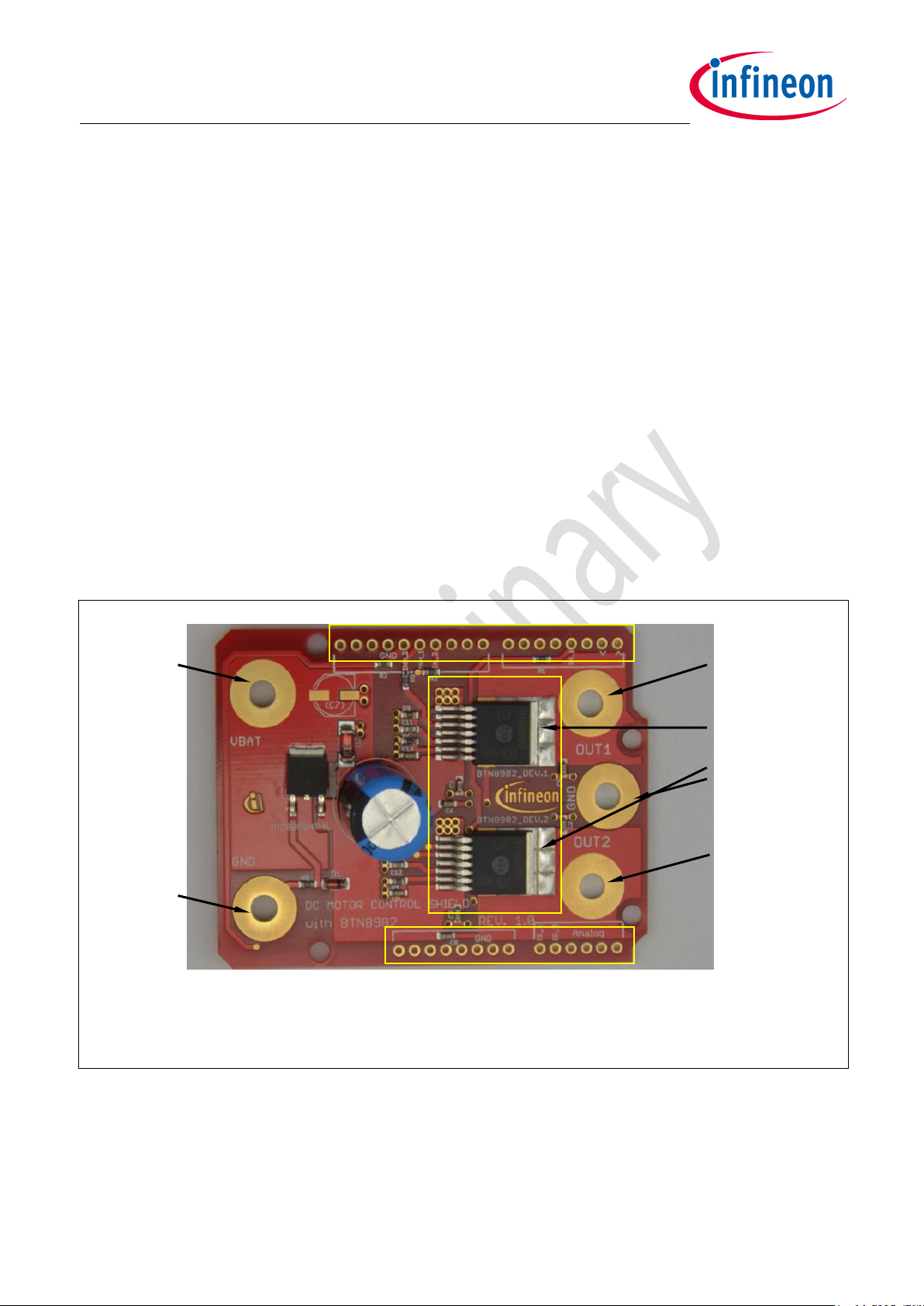
The Motor Control Shield adds powerful motor control to the Arduino projects. The shield can be controlled
with the general logic IO-Ports of a microcontroller. Either an Arduino Uno R3 or the XMC1100 Boot Kit from
Infineon can be used as the master.
On board of the Motor Control Shield are two BTN8982TA NovalithICTM. Each is featuring one P-channel high
side MOSFET and one N-channel low side MOSFET with an integrated driver IC in one package. Due to the Pchannel high side switch a charge pump is not needed.
The BTN8982TA half-bridge is easy to control by applying logic level signals to the IN and INH pin. When
applying a PWM to the IN pin the current provided to the motor can be controlled with the duty cycle of the
PWM. With an external resistor connected between the SR pin and GND the slew rate of the power switches
can be adjusted.
The Motor Control Shield can be easily connected to any Arduino board or the XMC1100 Boot Kit via
headers.
Figure 1 Motor Control Shield photo
1.2 Key features
The Motor Control Shield has the following features:
An Arduino Uno R3, XMC1100 Boot Kit, or similar board connected to the shield can control the two half-
Users Manual 4 V0.9, 2015-03
bridges via the general IO pins.
TM
Page 5

1
2
3
4
5
6
7
8
9
10
11
12
13
14
15
16
17
18
19
20
21
22
23
Motor Control Shield with BTN8982TA
for Arduino
Brushed DC Motor Control up to 250 W continuous load
Drives either one brushed bi-directional DC motor or two uni-directional DC motors.
Capable of high frequency PWM, e.g. 30 kHz
Adjustable slew rates for optimized EMI by changing external resistor
Driver circuit with logic level inputs
Status flag diagnosis with current sense capability
Protection e.g. against overtemperature and overcurrent
Reverse polarity protection with IPD90P04P4L
Further comments:
o 8-18 V nominal input voltage (max. 6 – 40 V)
o Average motor current 30 A restricted due to the limited power dissipation of the PCB
(BTN8982TA current limitation @ 55 A min.)
o To keep the costs as low as possible the pin headers and connectors are not attached to the
shield. The user can solder them by himself. The pin headers are not expensive, but the
through whole soldering is a not insignificant cost factor.
o The size of the DC-link capacity (C4 in the schematics and C10 in the application circuit.)
with 1000µF is for most applications oversized. It is a worst case scenario if a 500W motor is
connected to the shield. The capacity can be replaced by smaller capacities when using less
powerful motors. Equation 10 in the BTN8960 /62 /80 /82 High Current PN Half Bridge
NovalithICTM (Rev. 0.3, 2014-09-11) Application Note should be used to calculate the value
of the DC-link capacity.
Figure 2 Motor Control Shield driving an engine cooling fan
Users Manual 5 V0.9, 2015-03
Page 6
Motor Control Shield with BTN8982TA
1
2
3
4
5
6
7
8
optional
M
XC866
TLE
4278G
I/O
Reset
Vdd
Vss
WO
RO
Q
D
GND
I
Microcontroller Voltage Regulator
C
19
100nF
C
D
47nF
C
Q
22µF
C
10
1000µF
R
11
10k
R
12
10k
R
111
0..51k
R
112
1k
I/OI/O
C
I
470nF
C
1O2V
220nF
C
1OUT
220nF
C
2O2V
220nF
C
2OUT
220nF
C
29
100nF
R
211
0..51k
I/OA/D
R
22
10k
R
21
10k
R
212
1k
A/D
INH
IN
IS
SR
BTN8982TA
VS
OUT
GND
INH
IN
IS
SR
BTN8982TA
VS
OUT
GND
V
S
Reverse Polarity
Protection
(IPD90P03P4L-04)
R
3
10k
D
Z1
10V
C
1
100nF
L
1
C
22
100nF
C
2IS
1nF
C
1IS
1nF
C
12
100nF
for Arduino
1.3 Block diagram of a bi-directional Motor Control
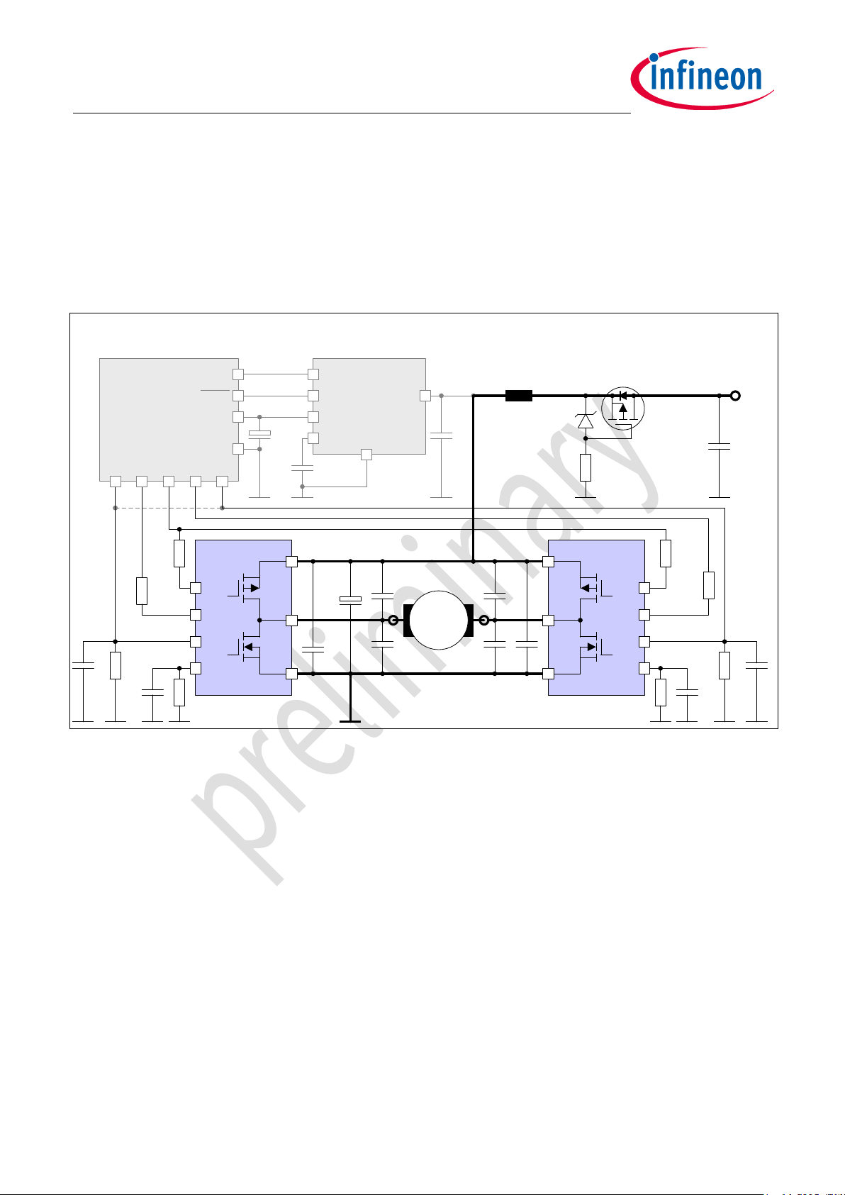
As a starting point for the Motor Control Shield, the application block diagram shown in Figure 3 was used.
For simplicity reasons the conductivity L1 was removed in the Shield schematics. In the application block
diagram the INH pins of both half-bridges are connected to one IO-port of the microcontroller. To be more
flexible in the usage of the Motor Control Shield each INH of the two half-bridges is connected to a separate
IO pin.
Figure 3 Application circuit for a bi-directional motor control with BTN8982TA
Users Manual 6 V0.9, 2015-03
Page 7

1
2
3
4
5
6
7
8
9
10
11
12
13
14
15
16
Motor Control Shield with BTN8982TA
for Arduino
2 Motor Control Shield board description
For a safe and sufficient motor control design, discrete components are needed. Some of them must be
dedicated to the motor application and some to the NovalithIC™.
Figure 4, Figure 5 and Figure 6 show the schematics plus the corresponding layout of the Motor Control
Shield.
Due to the possibility of using the Shield with loads which can draw a current of up to 55 A the connectors
Vbat, GND, OUT1 and OUT2 are designed as solid 4mm through whole connectors. This provides the
possibility to connect plugs which are capable of such high currents. Nevertheless the thermal performance
of the Shield itself limits the possible current which should be applied to the Motor Control Shield to 30 A. To
reach the best performance in terms of parasitic inductance and EMC a GND plane, with maximal size was
designed.
2.1 Schematics
In Figure 4 the schematics of the Motor Control Shield is shown. The schematics are based on the
application circuit in the BTN8982TA Data Sheet.
Figure 4 Schematics Motor Control Shield for Arduino with BTN8982TA
Users Manual 7 V0.9, 2015-03
Page 8

Motor Control Shield with BTN8982TA
1
2
3
4
5
6
7
for Arduino
2.2 Layout
Figure 5 and Figure 6 show the layout of the Motor Control Shield. The layout follows the design rules in the
BTN8960 /62 /80 /82 High Current PN Half Bridge NovalithICTM Application Note (also see Chapter 2.3).
Figure 5 Motor Control Shield – Bottom and top layers
Figure 6 Motor Control Shield for Arduino with BTN8982TA – Layout
Users Manual 8 V0.9, 2015-03
Page 9

Motor Control Shield with BTN8982TA
1
2
3
4
5
6
7
8
9
10
11
12
13
14
15
16
for Arduino
Figure 7 Motor Control Shield for Arduino with BTN8982TA – Bill of Material (BOM)
2.3 Important design and layout rules:
The basis for the following design and layout recommendations is the parasitic inductance of electrical
wires and design guidelines as described in Chapter three and four of the Application Note BTN8960 /62 /80
/82 High Current PN Half Bridge NovalithICTM (Rev. 0.3, 2014-09-11).
C4, so called DC-link capacitor: This electrolytic capacitor is required to keep the voltage ripple at the Vs-
pin of the NovalithIC™ low during switching operation (the applied measurement procedure for the
supply voltage is described in Chapter 3.1 of the Application Note). It is strongly recommended that the
voltage ripple at the NovalithIC™ Vs-pin to the GND-pin is kept below 1 V peak to peak. The value of C4
must be aligned accordingly. See therefore Equation (10) in the Application Note. Most electrolytic
capacitors are less effective at cold temperatures. It must be assured that C4 is also effective under the
worst case conditions of the application. The layout is very important too. As shown in Figure 6, the
capacitor C4 must be positioned with very short wiring close to the NovalithIC™. This must be done to
keep the parasitic inductors of the PCB-wires as small as possible.
Users Manual 9 V0.9, 2015-03
Page 10

1
2
3
4
5
6
7
8
9
10
11
12
13
14
15
16
17
18
19
20
21
22
23
24
25
26
27
28
29
30
31
32
Motor Control Shield with BTN8982TA
for Arduino
C1/C3: This ceramic capacitors support C4 to keep the supply voltage ripple low and cover the fast
transients between the Vs-pin and the GND-pin. The value of these ceramic capacitors must be chosen
so that fast Vs-ripples at the NovalithIC™ do not exceed 1V peak to peak. The layout wiring for C1/C3
must be shorter than for C4 to the NovalithIC™ to keep the parasitic PCB-wire inductance as small as
possible. In addition the parasitic inductance could be kept low by placing at least two vias for the
connection to the GND-layer.
C6/C8: These ceramic capacitors are important for EMI in order to avoid entering RF into the NovalithIC™
as much as possible. Good results have been achieved with a value of 220 nF. In terms of layout, it is
important to place these capacitors between “OUT” and “Vs” without significant additional wiring from
C6/C8 to the Vs- and OUT-line.
C5/C2: These ceramic capacitor help to improve the EMC immunity and the ESD performance of the
application. Good results have been achieved with a value of 220 nF. To keep the EMC and ESD out of the
board, the capacitor is most effective when positioned directly next to the board connector. In addition,
the parasitic inductance could be kept low by placing at least two vias for the connection to the GNDlayer.
Other components:
IC0, D1 and R8: Reverse polarity protection. See Chapter 4.4 of the Applikation Note.
R9/R6: Slew rate resistors according to data sheet.
C11/C12: Stabilization for slew rate resistors (R9/R6).
R7/R4: Resistors to generate a current sensing voltage from the IS current.
C10/C9: Ceramic capacitors for EMC immunity improvement. GND connection with at least two GND-
vias. A good value is 1nF. In case the current should be measured during the PWM-phase this capacitor
must be adapted to the ON-time inside the PWM-phase.
R1, R2, R3 and R5: Device protection in case of microcontroller pins shorted to Vs.
2.4 Pin assignment
To use the Motor Control Shield the necessary control signals can be applied directly at the ArduinoTM
connectors. There is no need to use an Arduino or XMC 1100 Boot Kit to get the Motor Control Shield into an
application. The control pins are logic level inputs which can be driven by any other microcontroller or with
logic level signals. Besides the supply voltage Vbat has to be provided to the Vbat connector. Figure 8 shows
the pinout/connectors of the Motor Control Shield.
Users Manual 10 V0.9, 2015-03
Page 11

Motor Control Shield with BTN8982TA
1
2
3
Pin
Symbol
I/O
Function
GND
GND
-
Ground
D3
IN_1
I
Input bridge 1
Defines whether high- or low side switch is activated
D11
IN_2
I
Input bridge 2
Defines whether high- or low side switch is activated
D12
INH_1
I
Inhibit bridge 1
When set to low device goes in sleep mode
D13
INH_2
I
Inhibit bridge 2
When set to low device goes in sleep mode
OUT_1
OUT_1
O
Power output of the bridge 1
OUT_2
OUT_2
O
Power output of the bridge 2
A0
IS_1
O
Current Sense and Diagnostics of half-bridge 1
A1
IS_2
O
Current Sense and Diagnostics of half-bridge 2
Vbat
Vbat
-
Supply (Vs after the reverse polarity protection)
Vbat
GND
OUT1
NovalithIC
TM
BTN8982TA
GND
OUT2
INH_2
IN_2
IN_1
GND
GND
for Arduino
2x
Figure 8 Motor Control Shield connectors
2.5 Pin definitions and functions
Users Manual 11 V0.9, 2015-03
Page 12

1
2
3
4
5
6
7
8
9
10
11
12
13
14
15
16
17
18
19
20
21
22
23
24
25
26
27
28
29
Motor Control Shield with BTN8982TA
for Arduino
3 BTN8982TA overview
The BTN8982TA used in the Motor Control Shield is an integrated high current half-bridge for motor drive
applications. It is part of the NovalithIC™ family containing one p-channel high side MOSFET and one nchannel low side MOSFET with an integrated driver IC in one package. Due to the p-channel high side switch
the need for a charge pump is eliminated thus minimizing EMI. Interfacing to a microcontroller is made easy
by the integrated driver IC which features logic level inputs, diagnosis with current sense, slew rate
adjustment, dead time generation and protection against overtemperature, undervoltage, overcurrent and
short circuit.
The BTN8982TA provides a cost optimized solution for protected high current PWM motor drives with very
low board space consumption.
3.1 Key features of the BTN8982TA NovalithIC
Path resistance of max. 20.4 mΩ @ 150 °C (typ. 10.0 mΩ @ 25 °C)
High side: max. 10.5 mΩ @ 150 °C (typ. 5.3 mΩ @ 25 °C)
Low side: max. 9.9 mΩ @ 150 °C (typ. 4.7 mΩ @ 25 °C)
Enhanced switching speed for reduced switching losses
Capable for high PWM frequency combined with active freewheeling
Low quiescent current of typ. 7 µA @ 25 °C
Switched mode current limitation for reduced power dissipation in overcurrent
Current limitation level of 55 A min.
Status flag diagnosis with current sense capability
Overtemperature shut down with latch behavior
Undervoltage shut down
Driver circuit with logic level inputs
Adjustable slew rates for optimized EMI
Operation up to 40 V
Green Product (RoHS compliant)
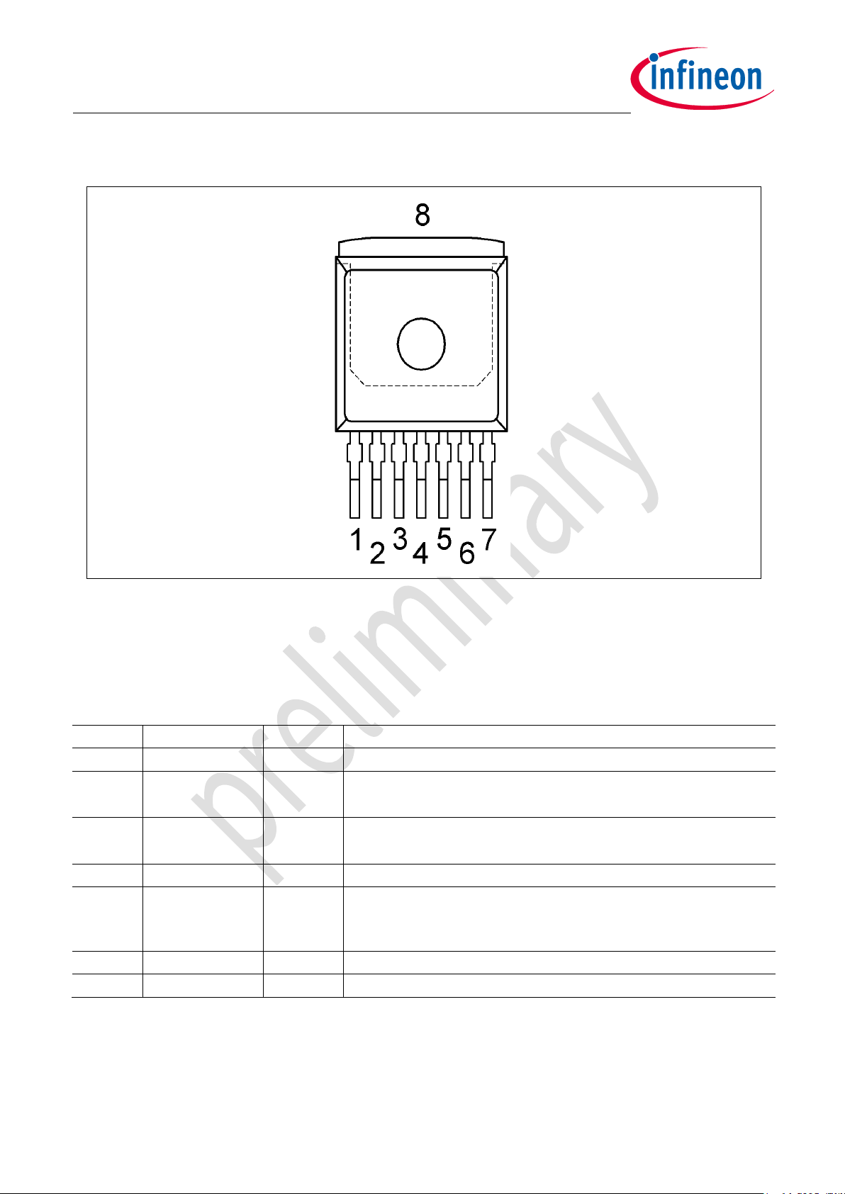
AEC Qualified in PG-TO263-7-1 package
TM
Figure 9 PG-TO263-7-1
Users Manual 12 V0.9, 2015-03
Page 13
1
2
3
4
5
6
7
8
9
10
11
12
13
IS
SR
INH
IN
GND
OUT
VS
Gate Driver
HS
Slewrate
Adjustment
Digital Logic
Undervolt.
detection
Overtemp.
detection
Current
Limitation
LS
Current
Limitation
HS
Current
Sense
Gate Driver
LS
LS off HS off
Motor Control Shield with BTN8982TA
for Arduino
3.2 Block diagram
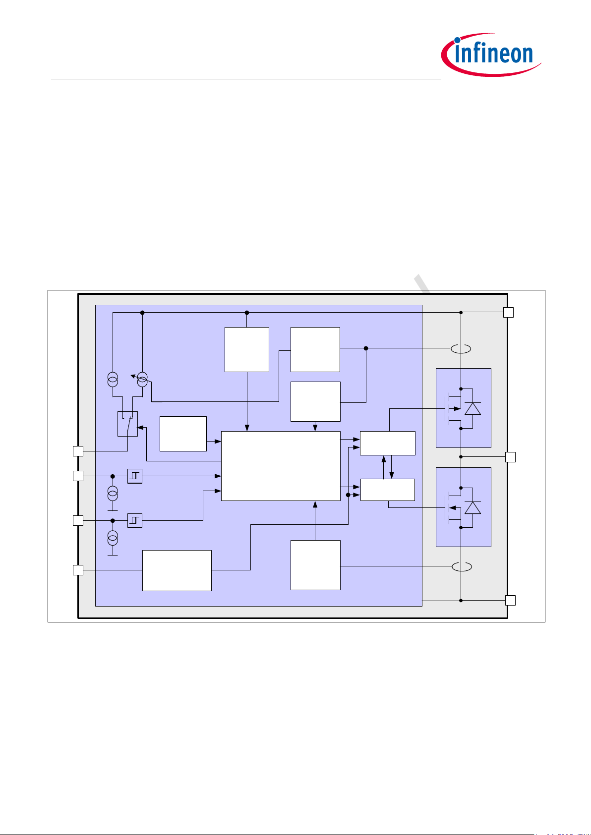
The BTN8982TA is part of the NovalithIC™ family containing three separate chips in one package: One p-
channel high side MOSFET and one n-channel low side MOSFET together with a driver IC, forming an
integrated high current half-bridge. All three chips are mounted on one common lead frame, using the chip
on chip and chip by chip technology. The power switches utilize vertical MOS technologies to ensure
optimum on state resistance.
Due to the p-channel high side switch the need for a charge pump is eliminated thus minimizing EMI.
Interfacing to a microcontroller is made easy by the integrated driver IC which features logic level inputs,
diagnosis with current sense, slew rate adjustment, dead time generation and protection against
overtemperature, undervoltage, overcurrent and short circuit. The BTN8982TA can be combined with other
BTN8982TA to form H-bridge and 3-phase drive configurations.
Figure 10 Block diagram BTN8982TA
Users Manual 13 V0.9, 2015-03
Page 14
Motor Control Shield with BTN8982TA
1
2
3
4
5
Pin
Symbol
I/O
Function
1
GND
-
Ground
2
IN
I
Input
Defines whether high- or low side switch is activated
3
INH
I
Inhibit
When set to low device goes in sleep mode
4, 8
OUT
O
Power output of the bridge
5
SR
I
Slew Rate
The slew rate of the power switches can be adjusted by
connecting a resistor between SR and GND
6
IS O Current Sense and Diagnostics
7
Vs - Supply (Vbat at the Shield connector)
6
7
for Arduino
3.3 Pin assignment
Figure 11 Pin assignment BTN8982TA (top view)
3.4 Pin definitions and functions BTN8982TA
Table 2
Users Manual 14 V0.9, 2015-03
Page 15

1
2
3
4
5
6
7
8
9
10
11
12
13
14
15
16
17
18
19
20
21
22
23
24
25
26
27
Motor Control Shield with BTN8982TA
for Arduino
4 Getting Started
4.1 Target applications
The application targeted by the BTN89xx devices is brushed DC Motor Control. Besides Motor Control any
other inductive, resistive and capacitive load within the electrical characteristics of the NovalithIC
driven by the BTN89xx. In the Motor Control Shield two BTN8982TA are used. Each is capable of driving up to
50 A. The limited thermal performance of the Shield PCB limits the recommended maximum current to 30 A.
4.2 Typical target application
With the Motor Control Shield either two mid power uni-directional DC-brushed motors or one bi-directional
brushed motor (with the two half-bridges used in H-bridge configuration) can be driven. The half-bridges
are controlled via the IN (Input) and INH (Inhibit) pins. The slew rate of the high frequency PWM can be
adjusted by connecting an external resistor between the SR pin and GND. The BTM8982TA also provides a
sense current at the IS pin. The Power Shield provides a fast and easy access to brushed DC motor solutions
of up to 300 W.
TM
can be
4.2.1 Getting started: Shield
Choose a mid-power, brushed DC motor.
Choose a DC adapter. The nominal input of the Power Shield is 8 – 18 V DC. Maximum Voltage is 40 V
Select pin headers and connectors of your choice and solder to the Power Shield. Due to cost
reduction, the pin headers and connectors are not attached.
Connect the Power Shield to Arduino Uno R3 or XMC 1100 Boot Kit.
Connect power supply (5 V) to the Arduino Uno R3 or XMC 1100 Boot Kit (Micro USB). For the XMC
Boot Kit a standard mobile phone charger can be used.
Program the controller board with the motor control software (see 4.2.2).
Connect the motor to OUT1 and OUT2 (H-bridge). For bi-directional applications connect the motor
to OUT1 and OUT2 (H-bridge). For uni-directional use, the motor can be placed between an output
OUT1/OUT2 and either GND or Vbat (half-bridge).
Connect the DC adapter to the Power Shield (Vbat, GND).
Turn on the power.
Users Manual 15 V0.9, 2015-03
Page 16

Motor Control Shield with BTN8982TA
1
2
3
4
5
6
7
8
9
10
11
12
13
14
15
16
17
18
19
20
Vbat
GND
OUT1
NovalithIC
TM
BTN8982TA
GND
OUT2
INH_2
IN_2
IN_1
GND
GND
for Arduino
2x
Figure 12 Motor Control Shield connectors
4.2.2 Getting started: Software
A simple example software for the XMC1100 Boot Kit is provided (H-bridge).
Users Manual 16 V0.9, 2015-03
Connect the XMC 1100 Boot Kit with a micro USB cable to the USB port of your PC.
Download and install the DAVE
Infineon website DAVETM.
Start DAVE
TM
and import project file H-bridge:
TM
- Free Development Platform for Code Generation from the
Page 17

Motor Control Shield with BTN8982TA
1
2
3
4
5
6
7
8
for Arduino
1: Select File Import
2: Choose Infineon DAVE project
Users Manual 17 V0.9, 2015-03
Page 18

Motor Control Shield with BTN8982TA
1
2
3
4
5
6
7
8
9
10
11
12
13
14
for Arduino
3: Select archive file Browse for the file Select the project Click finish
4: Build the project:
5: Start the debugger:
Users Manual 18 V0.9, 2015-03
Page 19

Motor Control Shield with BTN8982TA
1
2
3
4
5
6
7
8
9
10
11
12
13
14
15
16
for Arduino
6: Run the software the motor will spin
4.2.3 Software hints
For hints, tutorials, software examples, a quick introduction and further information around the DAVE™ –
Free Development Platform for Code Generation, visit the DAVETM web site.
The DAVE
Figure 13. The output voltage is controlled by the two PWMSP001 Apps. The ramp time is controlled by a
third PWMSP001 App via interrupts. The inhibit signals are software controlled by the IO004 App.
TM
App structure of the software example H-bridge for the Motor Control Shield is shown in
Figure 13 App structure of the example software H-bridge
To change the PWM frequency from 25 kHz to a different value the settings of both PWM App instances
PWMSP001/0 and PWMSP001/0 have to be modified. There, the PWM frequency can be easily set to different
values.
Users Manual 19 V0.9, 2015-03
Page 20

Motor Control Shield with BTN8982TA
1
2
3
4
5
6
7
for Arduino
Figure 14 shows the ramp generator and the parameters which can be set in main.c. The parameter
“outputvoltage_max” and “outputvoltage_min” are controlled in the software by adapting the PWM
duty cycle. With the duty cycle the motor speed and current consumption in controlled.
Figure 14 Ramp generator and its parameters
Users Manual 20 V0.9, 2015-03
Page 21

Motor Control Shield with BTN8982TA
1
2
Page or Reference
Description of change
V0.9, 2015-03
for Arduino
Revision History
Major changes since the last revision
Users Manual 21 V0.9, 2015-03
Page 22

Published by
Infineon Technologies AG
81726 Munich, Germany
© 2015 Infineon Technologies AG.
All Rights Reserved.
Order Number:
B127-10043-V1-7600-EU-EC-P
Legal Disclaimer
The information given in this document shall in
no event be regarded as a guarantee of
conditions or characteristics. With respect to any
examples or hints given herein, any typical values
stated herein and/or any information regarding
the application of the device, Infineon
Technologies hereby disclaims any and all
warranties and liabilities of any kind, including
without limitation, warranties of noninfringement of intellectual property rights of any
third party.
Information
For further information on technology, delivery
terms and conditions and prices, please contact
the nearest Infineon Technologies Office
(www.infineon.com).
Warnings
Due to technical requirements, components may
contain dangerous substances. For information on
the types in question, please contact the nearest
Infineon Technologies Office. Infineon Technologies
components may be used in life-support devices or
systems only with the express written approval of
Infineon Technologies, if a failure of such components
can reasonably be expected to cause the failure of
that life-support device or system or to affect the
safety or effectiveness of that device or system. Life
support devices or systems are intended to be
implanted in the human body or to support and/or
maintain and sustain and/or protect human life. If
they fail, it is reasonable to assume that the health of
the user or other persons may be endangered.
www.infineon.com
Trademarks of Infineon Technologies AG
AURIX™, C166™, CanPAK™, CIPOS™, CIPURSE™, CoolGaN™, CoolMOS™, CoolSET™, CoolSiC™, CORECONTROL™, CROSSAVE™, DAVE™, DI-POL™, DrBLADE™,
EasyPIM™, EconoBRIDGE™, EconoDUAL™, EconoPACK™, EconoPIM™, EiceDRIVER™, eupec™, FCOS™, HITFET™, HybridPACK™, ISOFACE™, IsoPACK™, iWafer™, MIPAQ™, ModSTACK™, my-d™, NovalithIC™, OmniTune™, OPTIGA™, OptiMOS™, ORIGA™, POWERCODE™, PRIMARION™, PrimePACK™,
PrimeSTACK™, PROFET™, PRO-SIL™, RASIC™, REAL3™, ReverSave™, SatRIC™, SIEGET™, SIPMOS™, SmartLEWIS™, SOLID FLASH™, SPOC™, TEMPFET™,
thinQ!™, TRENCHSTOP™, TriCore™.
Other Trademarks
Advance Design System™ (ADS) of Agilent Technologies, AMBA™, ARM™, MULTI-ICE™, KEIL™, PRIMECELL™, REALVIEW™, THUMB™, µVision™ of ARM
Limited, UK. ANSI™ of American National Standards Institute. AUTOSAR™ of AUTOSAR development partnership. Bluetooth™ of Bluetooth SIG Inc. CAT-
iq™ of DECT Forum. COLOSSUS™, FirstGPS™ of Trimble Navigation Ltd. EMV™ of EMVCo, LLC (Visa Holdings Inc.). EPCOS™ of Epcos AG. FLEXGO™ of
Microsoft Corporation. HYPERTERMINAL™ of Hilgraeve Incorporated. MCS™ of Intel Corp. IEC™ of Commission Electrotechnique Internationale. IrDA™ of
Infrared Data Association Corporation. ISO™ of INTERNATIONAL ORGANIZATION FOR STANDARDIZATION. MATLAB™ of MathWorks, Inc. MAXIM™ of
Maxim Integrated Products, Inc. MICROTEC™, NUCLEUS™ of Mentor Graphics Corporation. MIPI™ of MIPI Alliance, Inc. MIPS™ of MIPS Technologies, Inc.,
USA. muRata™ of MURATA MANUFACTURING CO., MICROWAVE OFFICE™ (MWO) of Applied Wave Research Inc., OmniVision™ of OmniVision Technologies,
Inc. Openwave™ of Openwave Systems Inc. RED HAT™ of Red Hat, Inc. RFMD™ of RF Micro Devices, Inc. SIRIUS™ of Sirius Satellite Radio Inc. SOLARIS™ of
Sun Microsystems, Inc. SPANSION™ of Spansion LLC Ltd. Symbian™ of Symbian Software Limited. TAIYO YUDEN™ of Taiyo Yuden Co. TEAKLITE™ of CEVA,
Inc. TEKTRONIX™ of Tektronix Inc. TOKO™ of TOKO KABUSHIKI KAISHA TA. UNIX™ of X/Open Company Limited. VERILOG™, PALLADIUM™ of Cadence
Design Systems, Inc. VLYNQ™ of Texas Instruments Incorporated. VXWORKS™, WIND RIVER™ of WIND RIVER SYSTEMS, INC. ZETEX™ of Diodes Zetex.
Last Trademarks Update 2014-07-17
Edition 2015-03
ifx000000000001
 Loading...