
IRAUDAMP17
100W/4Ω x 2 Channel Class D Audio Power Amplifier
Using the IR4302
By
Jun Honda, Liwei Zheng
International Rectifier suggests the following guidelines for safe operation and
handling of IRAUDAMP17 Demo board;
Always wear safety glasses whenever operating Demo Board
Avoid physical contact with exposed metal surfaces when operating Demo
Board
Turn off Demo Board when placing or removing measurement probes
www.irf.com Page 1 of 13
CAUTION:
IRAUDAMP17 REV 1.1

TABLE OF CONTENTS ........................... PAGE
INTRODUCTION..............................................................................3
SPECIFICATIONS ...........................................................................3
CONNECTION SETUP ....................................................................4
TEST PROCEDURES......................................................................5
PERFORMANCE AND TEST GRAPHS ..........................................5
THERMAL INFORMATION..............................................................8
BILL OF MATERIALS ....................................................................10
PCB SPECIFICATIONS.................................................................11
REVISION CHANGES DESCRIPTIONS .......................................13
www.irf.com Page 2 of 13
IRAUDAMP17 REV 1.1
Introduction
The IRAUDAMP17 reference design is a two-channel, 100W/ch (4 Ω/52V Bus voltage) half-bridge
Class D audio power amplifier with single power supply. This reference design demonstrates how to
use the IR4302 IC with single power supply, implement protection circuits, and design an optimum
PCB layout using PowIRaudio integrated Class D IC. This reference design does not require
additional heatsink or fan cooling for normal operation (one-eighth of continuous rated power).The
reference design provides all the required housekeeping power supplies for ease of use. The twochannel design is scalable for power and the number of channels.
Applications
AV receivers
Home theater systems
Mini component stereos
Powered speakers
Sub-woofers
Musical Instrument amplifiers
Car audio amplifiers
Features
Output Power: 100W x 2 channels (10%THD+N 4Ω load; with heatsink),
60W x 2 channels (10%THD+N 4Ω load; no heatsink),
Multiple Protection Features: Over-current protection (OCP), high side and low side
Over-voltage protection (OVP),
Under-voltage protection (UVP), high side and low side
Over-temperature protection (OTP)
PWM Modulator: Self-oscillating half-bridge topology
Specifications
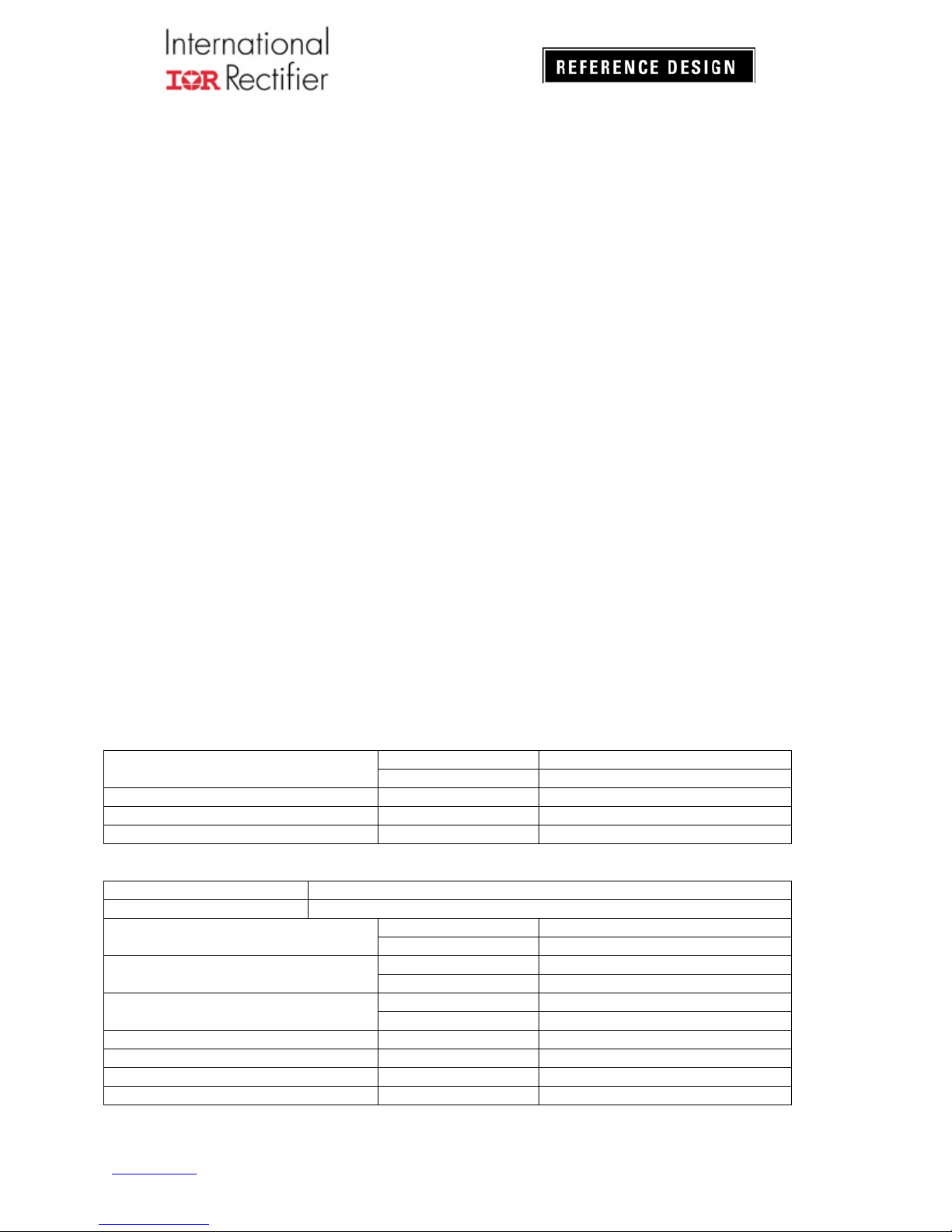
General Test Conditions (unless otherwise noted) Notes / Conditions
Supply Voltages
Load Impedance 2-4Ω Resistive load
Self-Oscillating Frequency 400kHz No input signal, Adjustable
Gain Setting 24.8dB 1Vrms input yields rated power
Electrical Data Typical Notes / Conditions
IR Devices Used IR4302 PowIRaudio integrated Class D IC
Modulator Self-oscillating, second order sigma-delta modulation, analog input
Power Supply Range
Output Power CH1-2: (1% THD+N)
Output Power CH1-2: (10% THD+N)
Rated Load Impedance 2-4Ω Resistive load
Idling Supply Current 65mA No input signal
Total Idle Power Consumption 3.4W No input signal
Distortion 0.008% THD+N @ 30W, 4Ω
40V~52V With heatsink
30V~42V *Without heatsink
40V~52V
30V~42V *Without heatsink
75W 1kHz, 4Ω load, with heatsink
50W 1kHz, 4Ω load, without heatsink
100W 1kHz, 4Ω load, with heatsink
60W 1kHz, 4Ω load, without heatsink
Single power supply;
www.irf.com Page 3 of 13
IRAUDAMP17 REV 1.1
Residual Noise
220V
Channel Efficiency 96%
*Need to change components as below to achieve 30V~42V power supply voltage range without heatsink
With Heatsink Without Heatsink
Power Supply Voltage Range 40~52V 30~42V
R7~R10 390Ω 240Ω
Z5 36V 27V
Connection Setup
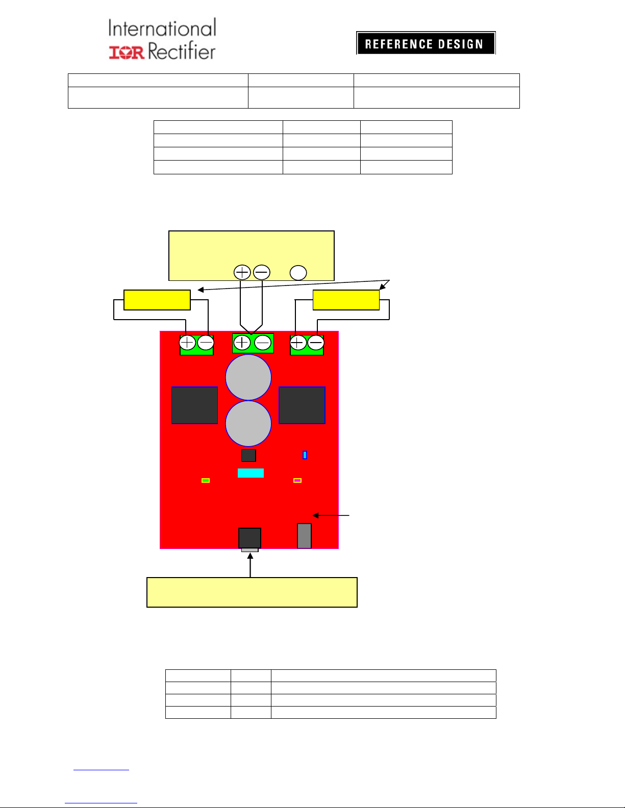
40-52V*, 3A DC supply
P1
P2
CH1
Output
P3
CH2
Output
IHF-A weighted, AES-17 filter
Single-channel driven,100W Class D
stage
* Without heatsink Power supply
voltage range is 30~42V
250W, Non-inductive Resistors
4 Ohm 4 Ohm
CLIP
Indicator
Audio Signal Generator
Connector Description
Audio IN CN1 Analog input for CH1 and CH2
POWER P3 Single supply
CH1 OUT P1 Output for CH1
CH2 OUT P2 Output for CH2
Audio
Input
Power
Indicator
IR4302
CN1
FAULT
Indicator
SW1
Fig 1 Typical Test Setup
SW1:PWM Shutdown/MUTE
www.irf.com Page 4 of 13
IRAUDAMP17 REV 1.1
Test Procedures
Test Setup:
1. Connect 4, 250W load to both output connectors, P1 and P2 and audio analyzer (Ap).
2. Connect Audio Signal Generator to CN1 for CH1 and CH2 respectively (Ap).
3. Connect a single power supply to P3 pre-adjusted to 40-52V as shown on Figure above
4. Turn on the power supply.
5. Turn on SW1 (right side).
6. Blue LED (Normal) stays turning on after RED LED extinguished.
7. With an Oscilloscope, monitor switching waveform at VS of CH1 and CH2.
8. Quiescent current for the power supply should be 70mA 10mA at 52V.
Functionality Audio Tests:
9. Sweep the audio signal voltage from 15 mV
10. Monitor the output signals at P1/P2 with an oscilloscope. The waveform must be a non
distorted sinusoidal signal with input sinusoidal signal below 1Vrms.
RMS
to 1.5 V
RMS
.
Performance and Test Graphs
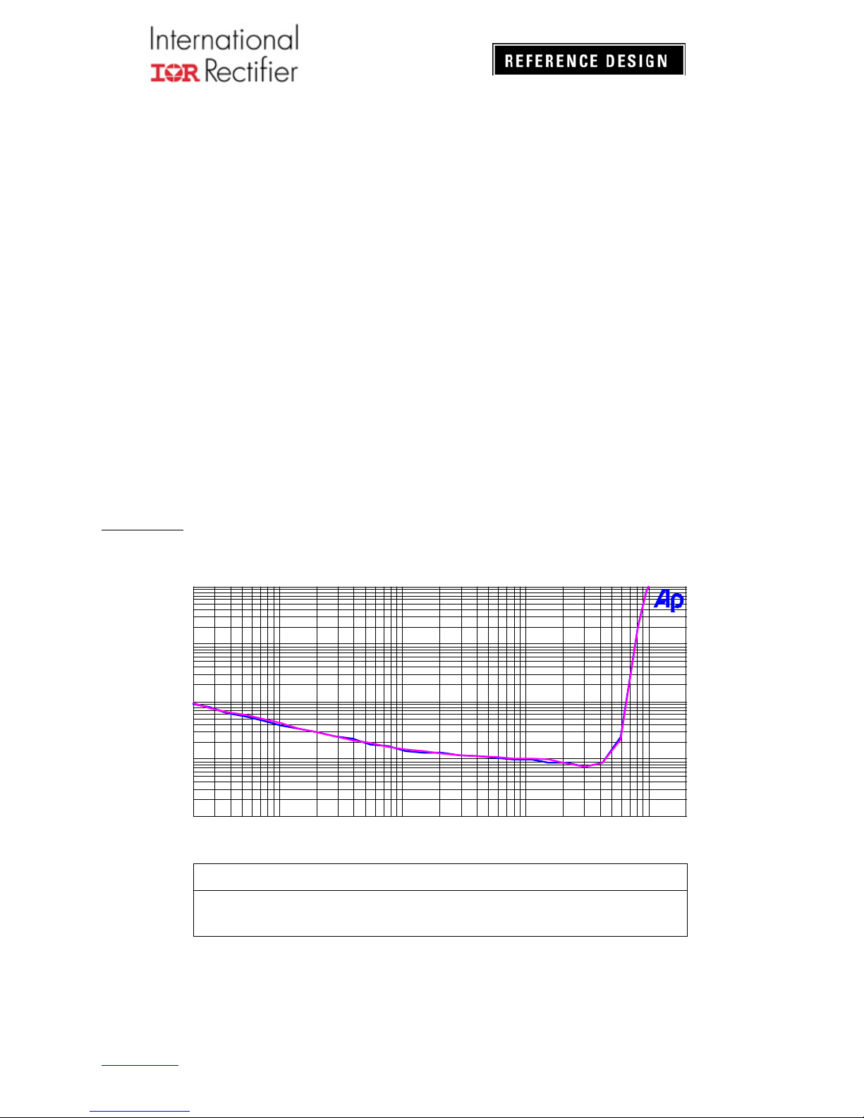
Power vs THD+N
Test Conditions:
Load Impedance = 4 ohms
VBus = 52V(with heatsink)
Input Signal=1 kHz
10
5
2
1
0.5
0.2
0.1
%
0.05
0.02
0.01
0.005
0.002
0.001
20m 20050m 100m 200m 500m 1 2 5 10 20 50 100
W
ColorSweep Trace Line Sty le Thick Data Axis Comment
1 1 Blue Solid 2 Anlr.THD+N Ratio Left CH1 4ohms 52V
1 3 Magenta Solid 2 Anlr.THD+N Ratio Left CH2 4ohms 52V
www.irf.com Page 5 of 13
Fig 2
IRAUDAMP17 REV 1.1
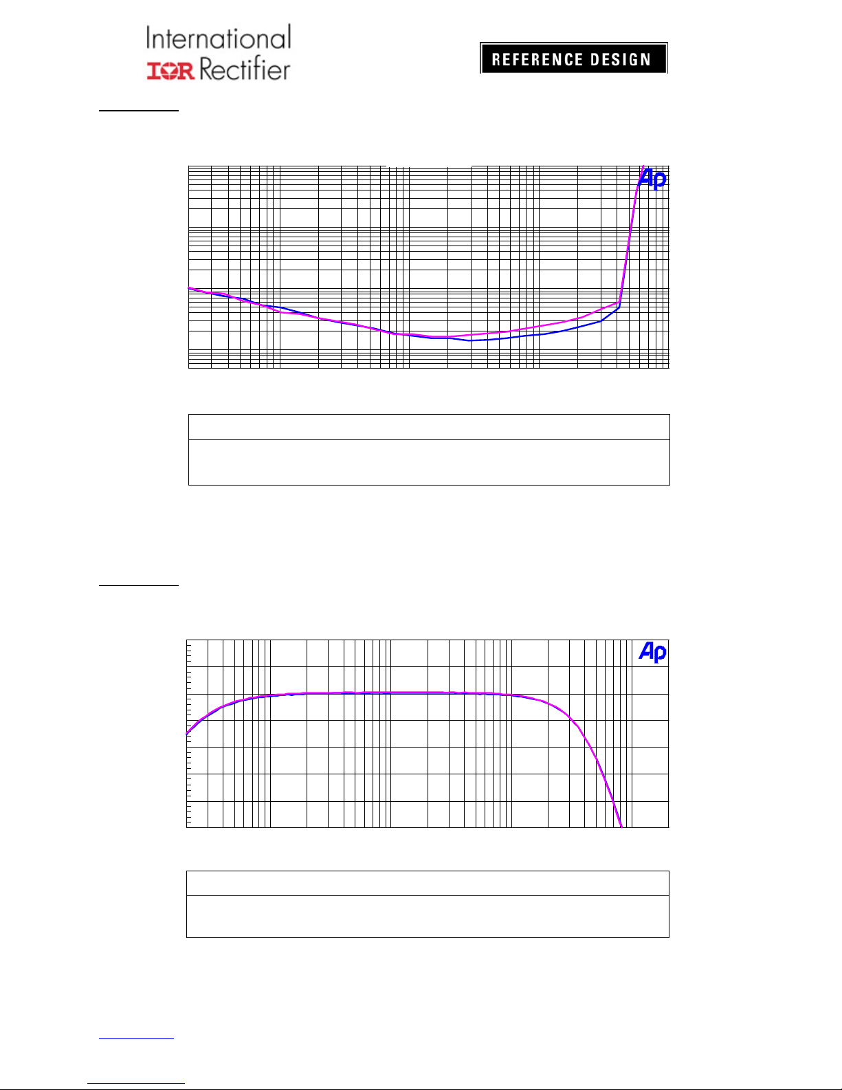
Test Conditions:
Load Impedance = 4 ohms
Frequency Response
VBus = 42V(without heatsink)
Input Signal=1 kHz
10
5
2
1
0.5
%
0.2
0.1
0.05
0.02
0.006
20m 10050m 100m 200m 500m 1 2 5 10 20 50
1 1 Blue Solid 2 Anlr.THD+N Ratio Left Ch1 42V 4ohms
1 3 Magenta Solid 2 Anlr.THD+N Ratio Left Ch2 42V 4ohms
Test Conditions:
Load Impedance = 4 ohms
VBus = 52V
Set Output = 1V
+4
THD+N vs Power
W
ColorSweep Trac e Line Style Thick Data Axis Comment
Fig 3
+2
+0
d
B
A
-2
r
-4
-6
-8
-10
20 200k50 100 200 500 1k 2k 5k 10k 20k 50k 100k
Hz
ColorSweep Trace Line Style Thick Data Ax is Comment
1 1 Blue Solid 2 Anlr.Level A Left Ch1 52V 4ohms
1 2 Magenta Solid 2 Anlr.Level B Left Ch2 52V 4ohms
Fig 4
www.irf.com Page 6 of 13
IRAUDAMP17 REV 1.1
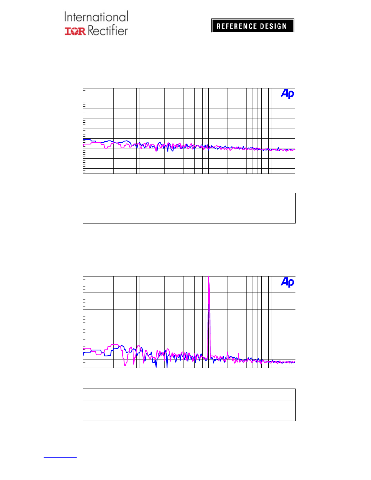
Noise Floor
Test Conditions:
Load Impedance = 4 ohms
No Input Signal
VBus = 52V
d
B
V
-100
-120
-140
+20
+0
-20
-40
-60
-80
10 20k20 50 100 200 500 1k 2k 5k 10k
Hz
ColorSweep Trace Line Sty le Thick Data Axis Comment
1 1 Blue Solid 2 Fft.Ch.1 Ampl Left Ch1
1 2 Magenta Solid 2 Fft.Ch.2 Am pl Left Ch2
Noise Floor with 1Vrms Output
Test Conditions:
Load Impedance = 4 ohms
VBus = 52V
Set Output= 1Vrms @ 1 KHz
+0
-20
-40
d
B
-60
V
-80
-100
10 20k20 50 100 200 500 1k 2k 5k 10k
Fig5
Hz
ColorS weep Trace Line Sty le Thick Data Axis Comment
1 1 Blue Solid 2 Fft.Ch.1 Ampl Left Ch1
1 2 Magenta Solid 2 Fft.Ch.2 Ampl Left Ch2
www.irf.com Page 7 of 13
Fig 6
IRAUDAMP17 REV 1.1
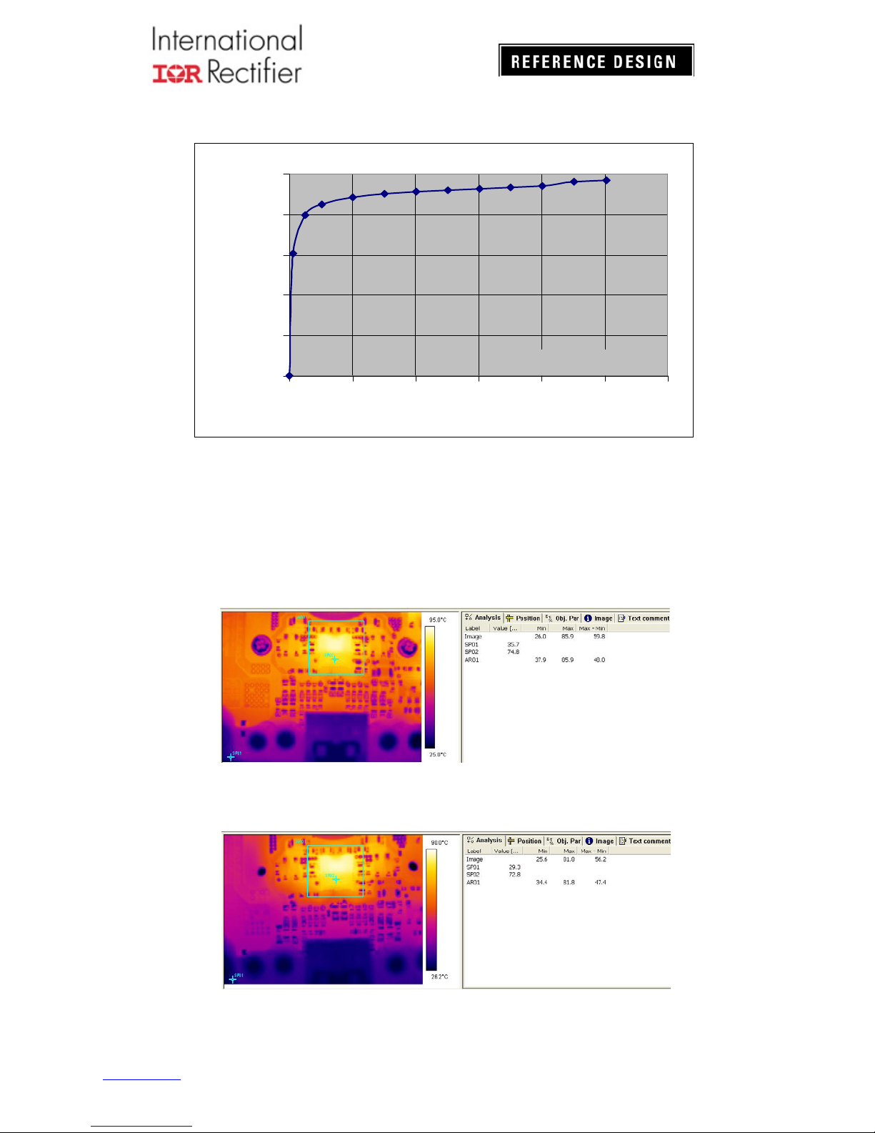
Efficiency
100.0%
80.0%
60.0%
40.0%
Efficiency
20.0%
0.0%
0 20406080100120
Thermal Information:
1/8 Po Thermal Test
Conditions:
Tamb=25°C natural convection cooling
Both Channel Driven 1/8Po continuous 30mins
Temperature measured by infrared camera
*Tested with heatsink
Power (W)
Fig 7
Fig 8 IRAUDAMP17 with heatsink (Vbus=52V)
IR4302’s temperature saturated around 85°C within 30minutes
Fig 9 IRAUDAMP17 without heatsink (Vbus=42V)
IR4302’s temperature saturated around 82°C within 30minutes
www.irf.com Page 8 of 13
IRAUDAMP17 REV 1.1

Schematic
Z5
*36V
R56
10k
R57
47k
+B
R55
+B
R52
+B
2
354
S1
1
OFF
UVP
47k
R53
10k
Z4
56V
10k
OVP
R51
47k
C35
6
ON
CT_PGND
0.1uF
SW SPDT
MMBT5551
Q2
SD
+B
C27
C25
0.1uF
0.1uF,100V
GND
MMBT5551
Q3
GND
1
2
P1
CT_P GND
LCH
R45 2.2k
D6
D7
R43
10, 1W
L1
C31
22uH
0.47uF, 400V
R41
1R
C33
+B
+
0.1uF, 63V
1
2
P3
+B
GND
2200uF, 63V
2200uF, 63V
C38
C39
C37
0.1uF,100V
C36
0.1uF,100V
R48 10k, 1/2WR4910k, 1/2W
GND
GND
-
P2
D8
L2
22uH
R42
1R
GND
R50
10R0
Dual Supply
10 Ohm
INPUT GND
R47
NM
CT_S GND CT_PGND
CT_PGND
1
2
CT_P GND
RCH
R46 2.2k
D9
C34
R44
10, 1W
0.1uF, 63V
C32
0.47uF, 400V
C28
0.1uF,100V
C26
0.1uF
Not m ounted
Singl e Suppl y
Not m ounted
10 Ohm
R47
R50
+B
+B
R40 9.1k
R35
1k 1W
R34 9.1k
23
C20
C19
0.1uF,50V
R32
33K
R30
4.7R
IC1
IR4302
VP2
24
D4
1N4148
VS2
1N4148
25
VB2
26
CSH2
27
COM
28
GND
NC
29
NC
30
DS2
1
R26
10K
C15 1nF
R24
180R
R22
2.2nF,50V
C11
C6
2.2nF,50V
1nF
GND
R8
CT_S GND
*390R 1W
SCH_DB_4302 Rev1.2
CP1
68k 1%
R15
R11
R3
D2
VAA
68k 1%
R16
R12
C1
1nF
C2
*3.01k 1%
*3.01k 1%
330
R4
330
CT_S GND
2.2uF
2.2uF
CP2
R1100k
Class D, AMP17 Schematic
VCC
23
22
21
VS2
VN2
VN1
OO
31
GND
-B
IN-23COM P 22CLIP
GND
IN+1
VSS
IN+2
5
4
180R
R19 180R
C12
2.2nF,50V
C7
2.2nF,50V
C5 10uF,10V
Z1
CT_SGND
R9
*390R 1W
IN-19COM P 1
VAA
8
6
7
R23
10uF,10V
R20 180R
C13
C10
C8
Z2
5.1V
2.2nF,50V
5.1V
R10
VSS
VAA
*390R 1W
INPUT GND
5
4
213
CN1
180R
20
VS1
CSD11FAULT
10
12
C17
1nF
R21 180R
C14 2.2nF,50V
2.2nF,50V
C9
2.2nF,50V
+B
R7
*390R 1W
0.1uF,50V
R33
33K
R31
4.7R
VP1
19
D5
1N4148
VS1
D3
1N4148
18
VB1
17
CSH1
16
COM
15
VCC
14
NC
13
DS1
R27
10K
R25
47K
D1
D10
C16
22uF, 16V
CP3
VSS
68k 1%
R17
R13
R5
VAA
SD
C3
*3.01k 1%
330
2.2uF
R2100k
R28
4.7R
C18
68k 1%
R18
R14
1nF
C4
1nF
*3.01k 1%
R6
330
CT_S GND
2.2uF
CP4
Z3
11V
MJD44H11T4G
1
Q1
CP5
R29
10K
DS3
GND
10uF,16V
GND
22uF
27V
240 Ohm
W itho ut H eatsink
36V
40-52V 30-42V
390ohm
With H e a ts ink
Power Supply
Voltage R a nge
R7,R8,R9,R10
*
CT_S GND
Z5
Fig 10
www.irf.com Page 9 of 13
IRAUDAMP17 REV 1.1

Bill of Materials
No Digikey P/N Designator Description Quantity Vender
1
399-1082-1-ND C1, C2, C3, C4, C15, C17 CAP CER 1000PF 50V 10% X7R 0603 6 Digikey
2
587-2668-1-ND C5, C10 CAP CER 10UF 10V 10% X7R 0805 2 Digikey
3
490-1500-1-ND
4
587-1433-1-ND C16 CAP CER 22UF 16V 20% X5R 1206 1 Digikey
5
490-5519-1-ND C18 CAP CER 10UF 16V 10% X6S 0805 1 Digikey
6
311-1140-1-ND C19, C20 CAP CER 0.1UF 50V 10% X7R 0805 2 Digikey
7
445-1418-1-ND C25, C26 CAP CER 0.1UF 100V 10% X7R 0805 2 Digikey
8
445-1377-1-ND C27, C28, C36, C37 CAP CER 0.1UF 100V 10% X7R 1206 4 Digikey
9
495-1315-ND C31, C32 CAP FILM 0.47UF 400VDC RADIAL 2 Digikey
10
BC2054-ND C33, C34 CAP FILM 0.1UF 63VDC RADIAL 2 Digikey
11
445-1418-1-ND C35 CAP CER 0.1UF 100V 10% X7R 0805 1 Digikey
12
565-1137-ND C38, C39 CAP ALUM 2200UF 63V 20% RADIAL 2 Digikey
13
CP1-3545N-ND CN1
14
565-1103-ND CP1, CP2, CP3, CP4 CAP ALUM 2.2UF 50V 20% RADIAL 4 Digikey
15
565-1056-ND CP5 CAP ALUM 22UF 25V 20% RADIAL 1 Digikey
16
1N4148W-FDICT-ND D1, D2, D3, D4, D5, D10
17
DFLU1200-7DICT-ND D6, D7, D8, D9 DIODE ULTRA FAST POWERDI 123 4 Digikey
18
160-1181-1-ND DS1 LED RED CLEAR 0603 SMD 1 Digikey
19
160-1183-1-ND DS2 LED GREEN CLEAR 0603 SMD 1 Digikey
20
160-1646-1-ND DS3 LED BLUE CLEAR 0603 SMD 1 Digikey
21
IR4302 IC1 2 CH PowIRaudio integrated Class D IC 1 IR
22
Sagami 7G17A-220M-R L1, L2 Power Inductors Class D Inductor 22uH 2
23
281-1414-ND P1, P2, P3
24
MJD44H11T4GOSCT-ND Q1 TRANS PWR NPN 8A 80V DPAK 1 Digikey
25
MMBT5551FSCT-ND Q2, Q3 TRANSISTOR NPN 160V SOT-23 2 Digikey
26
RMCF0603JT100KCT-ND R1, R2 RES 100K OHM 1/10W 5% 0603 SMD 2 Digikey
27
RMCF0603JT330RCT-ND R3, R4, R5, R6 RES 330 OHM 1/10W 5% 0603 SMD 4 Digikey
28
RMCF2512JT390RCT-ND R7, R8, R9, R10 RES 390 OHM 1W 5% 2512 SMD 4 Digikey
29
RHM3.01KCRCT-ND R11, R12, R13, R14 RES 3.01K OHM 1/8W 1% 0805 SMD 4 Digikey
30
311-68.0KCRCT-ND R15, R16, R17, R18 RES 68.0K OHM 1/8W 1% 0805 SMD 4 Digikey
31
RHM180GCT-ND
32
RHM47KGCT-ND R25 RES 47K OHM 1/10W 5% 0603 SMD 1 Digikey
33
RHM10KGCT-ND R26, R27, R29 RES 10K OHM 1/10W 5% 0603 SMD 3 Digikey
34
RMCF0603JT4R70CT-ND R28, R30, R31 RES TF 1/10W 4.7 OHM 5% 0603 3 Digikey
35
RHM33KGCT-ND R32, R33 RES 33K OHM 1/10W 5% 0603 SMD 2 Digikey
36
RHM9.1KARCT-ND R34, R40 RES 9.1K OHM 1/8W 5% 0805 SMD 2 Digikey
37
PT1.0KXCT-ND R35 RES 1.0K OHM 1W 5% 2512 SMD 1 Digikey
38
P1.0ACT-ND R41, R42 RESISTOR 1.0 OHM 1/8W 5% 0805 2 Digikey
39
541-10.0AFCT-ND R43, R44 RES 10.0 OHM 1W 1% 2512 SMD 2 Digikey
40
RMCF0805JT2K20CT-ND R45, R46 RES 2.2K OHM 1/8W 5% 0805 SMD 2 Digikey
41
541-10KVCT-ND R48, R49 RES 10K OHM 1/2W 5% 1210 SMD 2 Digikey
42
311-10ARCT-ND R50 RES 10 OHM 1/8W 5% 0805 SMD 1 Digikey
43
RHM47KARCT-ND R51, R55, R57 RES 47K OHM 1/8W 5% 0805 SMD 3 Digikey
C6, C7, C8, C9, C11, C12,
C13, C14
R19, R20, R21, R22, R23,
R24
CAP CER 2200PF 50V 10% X7R 0603 8 Digikey
CONN JACK STEREO R/A 5PIN
3.5MM
DIODE SWITCH 100V 400MW
SOD123
CONN TERM BLOCK PCB 5.0MM
2POS
RES 180 OHM 1/10W 5% 0603 SMD 6 Digikey
1 Digikey
6 Digikey
Inductors,
Inc
3 Digikey
www.irf.com Page 10 of 13
IRAUDAMP17 REV 1.1
44
RHM10KARCT-ND R52, R53, R56 RES 10K OHM 1/8W 5% 0805 SMD 3 Digikey
45
360-1758-ND S1
46
DDZ5V1BDICT-ND Z1, Z2 DIODE ZENER 5.1V 500MW SOD-123 2 Digikey
47
BZT52C11-FDICT-ND Z3 DIODE ZENER 11V 500MW SOD123 1 Digikey
MMSZ5263BT1GOSCT-
48
ND Z4 DIODE ZENER 56V 500MW SOD-123 1 Digikey
49
BZT52C36-FDICT-ND Z5 DIODE ZENER 36V 500MW SOD-123 1 Digikey
50
8401K-ND 1/2" Standoffs 4-40 STDOFF HEX M/F 4-40 .500"L ALUM 4 Digikey
51
H724-ND 4-40 Nut NUT HEX 4-40 STAINLESS STEEL 4 Digikey
52
H729-ND No. 4 Lock Washer WASHER LOCK INTERNAL #4 SS 4 Digikey
53
BER161-ND Thermal Pad THERMAL PAD .020" 4X4" GAPPAD 1/6 Digikey
SWITCH TOGGLE SPDT .4VA SEAL
PCB
1 Digikey
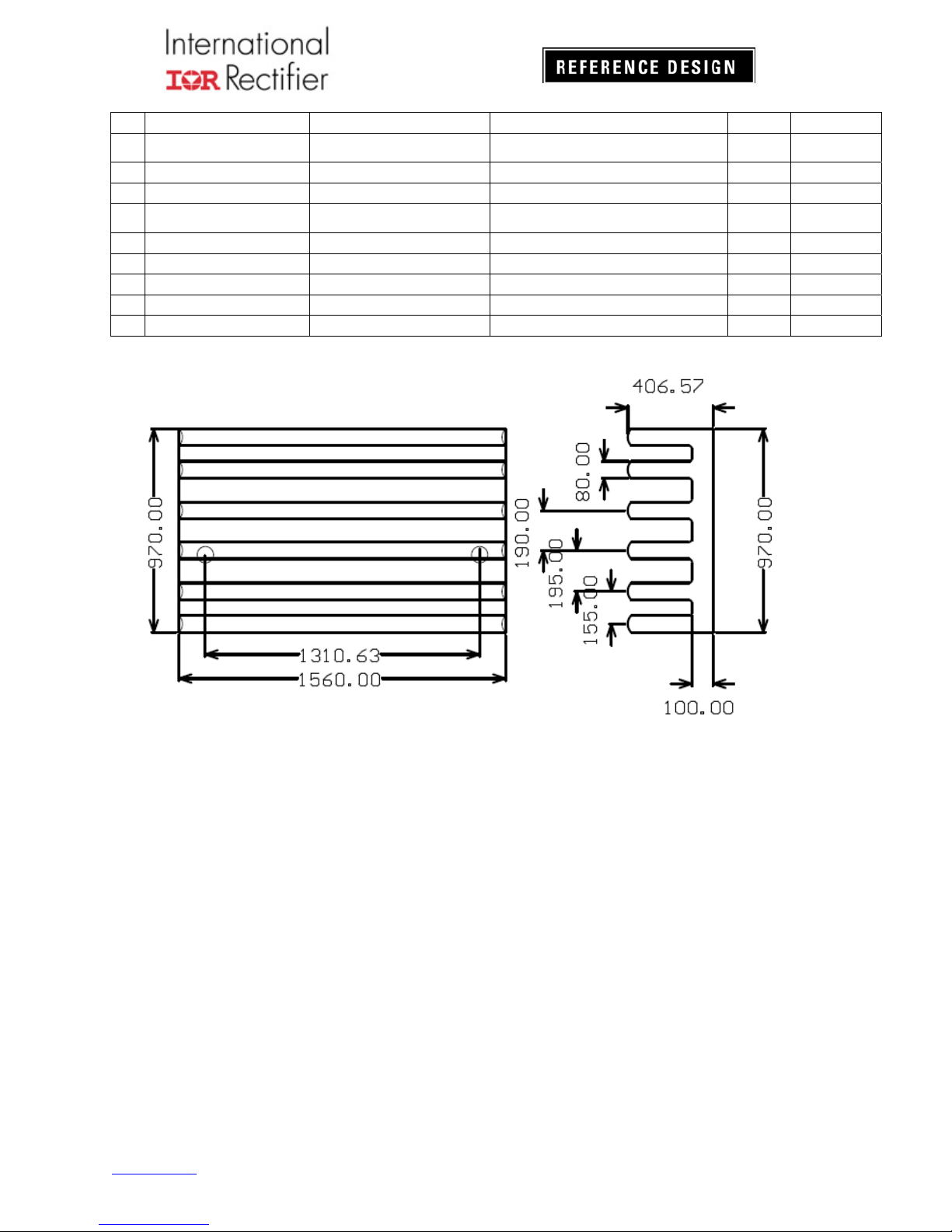
IRAUDAMP17 Heatsink
Fig11
PCB Specifications
PCB:
1. Two Layers SMT PCB with through holes
2. 1/16 thickness
3. 2/0 OZ Cu
4. FR4 material
5. 10 mil lines and spaces
6. Solder Mask to be Green enamel EMP110 DBG (CARAPACE) or Enthone Endplate
DSR-3241or equivalent.
7. Silk Screen to be white epoxy non conductive per IPC–RB 276 Standard.
8. All exposed copper must finished with TIN-LEAD Sn 60 or 63 for 100u inches thick.
9. Tolerance of PCB size shall be 0.010 –0.000 inches
10. Tolerance of all Holes is -.000 + 0.003”
11. PCB acceptance criteria as defined for class II PCB’S standards.
www.irf.com Page 11 of 13
IRAUDAMP17 REV 1.1

PCB Layout
Top side:
Bottom side:
Fig 12
Note: Refer to AN1170 for footprint and board mounting details.
www.irf.com Page 12 of 13
Fig 13
IRAUDAMP17 REV 1.1

Revision changes descriptions
Revision Changes description Date
Rev 1.0 Released May, 16 2012
Rev 1.1 BOM R50=10ohm May, 24 2012
WORLD HEADQUARTERS: 101 N. Sepulveda Blvd., El Segundo, California 90245 Tel: (310) 252-7105
Data and specifications subject to change without notice. 05/16/2012
www.irf.com Page 13 of 13
IRAUDAMP17 REV 1.1
 Loading...