


User Manual, V 1.7, January 2001
C166S V2
16-Bit Microcontroller
Microcontrollers
Never stop thinking.

Edition 2001-01
Published by Infineon Technologies AG,
St.-Martin-Strasse 53,
D-81541 München, Germany
© Infineon Technologies AG 2001.
All Rights Reserved.
Attention please!
The information herein is given to describe certain components and shall not be considered as warranted
characteristics.
Terms of delivery and rights to technical change reserved.
We hereby disclaim any and all warranties, including but not limited to warranties of non-infringement, regarding
circuits, descriptions and charts stated herein.
Infineon Technologies is an approved CECC manufacturer.
Information
For further information on technology, delivery terms and conditions and prices please contact your nearest
Infineon Technologies Office in Germany or our Infineon Technologies Representatives worldwide (see address
list).
Warnings
Due to technical requirements components may contain dangerous substances. For information on the types in
question please contact your nearest Infineon Technologies Office.
Infineon Technologies Components may only be used in life-support devices or systems with the express written
approval of Infineon Technologies, if a failure of such components can reasonably be expected to cause the failure
of that life-support device or system, or to affect the safety or effectiveness of that device or system. Life support
devices or systems are intended to be implanted in the human body, or to support and/or maintain and sustain
and/or protect human life. If they fail, it is reasonable to assume that the health of the user or other persons may
be endangered.

User Manual, V 1.7, January 2001
C166S V2
16-Bit Microcontroller
Microcontrollers
Never stop thinking.

C166S V2
Revision History: 2001-01 V1.7
Previous Version: Page Subjects (major changes since last revision)
We Listen to Your Comments
Any information within this document that you feel is wrong, unclear or missing at all?
Your feedback will help us to continuously improve the quality of this document.
Please send your proposal (including a reference to this document) to:
ce.cmd@infineon.com

User Manual
C166S V2
Table of Contents Page
1 Introduction . . . . . . . . . . . . . . . . . . . . . . . . . . . . . . . . . . . . . . . . . . . . . . . . 9
1.1 Technical Overview . . . . . . . . . . . . . . . . . . . . . . . . . . . . . . . . . . . . . . . . . . . 9
1.2 System Description . . . . . . . . . . . . . . . . . . . . . . . . . . . . . . . . . . . . . . . . . . 10
1.2.1 CPU . . . . . . . . . . . . . . . . . . . . . . . . . . . . . . . . . . . . . . . . . . . . . . . . . . . . 11
1.2.2 On-Chip Memory Modules . . . . . . . . . . . . . . . . . . . . . . . . . . . . . . . . . . . 12
1.2.3 Data Management Unit (DMU) . . . . . . . . . . . . . . . . . . . . . . . . . . . . . . . 12
1.2.4 Program Memory Unit (PMU) . . . . . . . . . . . . . . . . . . . . . . . . . . . . . . . . 12
1.2.5 Interrupt and PEC Controller . . . . . . . . . . . . . . . . . . . . . . . . . . . . . . . . . 13
1.2.6 OCDS and JTAG . . . . . . . . . . . . . . . . . . . . . . . . . . . . . . . . . . . . . . . . . . 13
1.2.7 External Bus Controller (EBC) . . . . . . . . . . . . . . . . . . . . . . . . . . . . . . . . 13
1.2.8 System Control Unit (SCU) . . . . . . . . . . . . . . . . . . . . . . . . . . . . . . . . . . 13
1.2.9 Clock Generation Unit (CGU) . . . . . . . . . . . . . . . . . . . . . . . . . . . . . . . . 14
1.2.10 On-Chip Bootstrap Loader . . . . . . . . . . . . . . . . . . . . . . . . . . . . . . . . . . . 14
2 Central Processing Unit . . . . . . . . . . . . . . . . . . . . . . . . . . . . . . . . . . . . . 15
2.1 Register Description Format . . . . . . . . . . . . . . . . . . . . . . . . . . . . . . . . . . . 17
2.2 CPU Special Function Registers . . . . . . . . . . . . . . . . . . . . . . . . . . . . . . . . 18
2.3 Instruction Fetch and Program Flow Control . . . . . . . . . . . . . . . . . . . . . . . 19
2.3.1 Branch Target Addressing Modes . . . . . . . . . . . . . . . . . . . . . . . . . . . . . 20
2.3.2 Branch Detection and Branch Prediction . . . . . . . . . . . . . . . . . . . . . . . . 22
2.3.3 Sequential and Mispredicted Instruction Flow . . . . . . . . . . . . . . . . . . . . 24
2.3.3.1 Correctly Predicted Instruction Flow . . . . . . . . . . . . . . . . . . . . . . . . . 24
2.3.3.2 Incorrectly Predicted Instruction Flow . . . . . . . . . . . . . . . . . . . . . . . . 26
2.3.4 Atomic and Extend Instructions . . . . . . . . . . . . . . . . . . . . . . . . . . . . . . . 27
2.3.5 Code Addressing via Code Segment and Instruction Pointer . . . . . . . . 28
2.3.6 IFU Control Registers . . . . . . . . . . . . . . . . . . . . . . . . . . . . . . . . . . . . . . 30
2.3.6.1 The CPU Configuration Register CPUCON1 . . . . . . . . . . . . . . . . . . . 30
2.3.6.2 The CPU Configuration Register CPUCON2 . . . . . . . . . . . . . . . . . . . 31
2.4 Use of General Purpose Registers . . . . . . . . . . . . . . . . . . . . . . . . . . . . . . 34
2.4.1 Memory Mapped GPR Banks and the Global Register Bank . . . . . . . . 36
2.4.2 Local Register Bank . . . . . . . . . . . . . . . . . . . . . . . . . . . . . . . . . . . . . . . . 40
2.4.3 Context Switch . . . . . . . . . . . . . . . . . . . . . . . . . . . . . . . . . . . . . . . . . . . . 40
2.4.3.1 Changing the selected Physical Register Bank . . . . . . . . . . . . . . . . . 40
2.4.3.2 Context Switching of the Global Register Bank . . . . . . . . . . . . . . . . . 42
2.5 Data Addressing . . . . . . . . . . . . . . . . . . . . . . . . . . . . . . . . . . . . . . . . . . . . 45
2.5.1 Short Addressing Modes . . . . . . . . . . . . . . . . . . . . . . . . . . . . . . . . . . . 46
2.5.2 Long and Indirect Addressing Modes . . . . . . . . . . . . . . . . . . . . . . . . . . 48
2.5.2.1 Addressing via Data Page Pointer DPP . . . . . . . . . . . . . . . . . . . . . . 49
2.5.2.2 DPP Override Mechanism in the C166S V2 CPU . . . . . . . . . . . . . . . 51
2.5.2.3 Long Addressing Mode . . . . . . . . . . . . . . . . . . . . . . . . . . . . . . . . . . . 52
2.5.2.4 Indirect Addressing Modes . . . . . . . . . . . . . . . . . . . . . . . . . . . . . . . . 53
2.5.3 DSP Addressing . . . . . . . . . . . . . . . . . . . . . . . . . . . . . . . . . . . . . . . . . . 56
2.5.4 The CoREG Addressing Mode . . . . . . . . . . . . . . . . . . . . . . . . . . . . . . . 63
User Manual 5 V 1.7, 2001-01

User Manual
C166S V2
Table of Contents Page
2.5.5 The System Stack . . . . . . . . . . . . . . . . . . . . . . . . . . . . . . . . . . . . . . . . . 64
2.6 Data Processing . . . . . . . . . . . . . . . . . . . . . . . . . . . . . . . . . . . . . . . . . . . . 68
2.6.1 Data Types . . . . . . . . . . . . . . . . . . . . . . . . . . . . . . . . . . . . . . . . . . . . . . 68
2.6.2 Constants . . . . . . . . . . . . . . . . . . . . . . . . . . . . . . . . . . . . . . . . . . . . . . . . 70
2.6.3 16-bit Adder/Subtracter, Barrel Shifter, and 16-bit Logic Unit . . . . . . . . 70
2.6.4 Bit Manipulation Unit . . . . . . . . . . . . . . . . . . . . . . . . . . . . . . . . . . . . . . . 70
2.6.5 Multiply and Divide Unit . . . . . . . . . . . . . . . . . . . . . . . . . . . . . . . . . . . . . 71
2.6.6 The Processor Status Word PSW . . . . . . . . . . . . . . . . . . . . . . . . . . . . . 74
2.7 Parallel Data Processing . . . . . . . . . . . . . . . . . . . . . . . . . . . . . . . . . . . . . . 78
2.7.1 Representation of Numbers and Rounding . . . . . . . . . . . . . . . . . . . . . . 79
2.7.2 The 16-bit by 16-bit signed/unsigned Multiplier and Scaler . . . . . . . . . . 80
2.7.3 Concatenation Unit . . . . . . . . . . . . . . . . . . . . . . . . . . . . . . . . . . . . . . . . 80
2.7.4 One-bit Scaler . . . . . . . . . . . . . . . . . . . . . . . . . . . . . . . . . . . . . . . . . . . . 80
2.7.5 The 40-bit Adder/Subtracter . . . . . . . . . . . . . . . . . . . . . . . . . . . . . . . . . 81
2.7.6 The Data Limiter . . . . . . . . . . . . . . . . . . . . . . . . . . . . . . . . . . . . . . . . . . 81
2.7.7 The Accumulator Shifter . . . . . . . . . . . . . . . . . . . . . . . . . . . . . . . . . . . . 82
2.7.8 The 40-bit Signed Accumulator Register . . . . . . . . . . . . . . . . . . . . . . . . 82
2.7.9 The Repeat Counter MRW . . . . . . . . . . . . . . . . . . . . . . . . . . . . . . . . . . 84
2.7.10 The MAC Unit Status Word MSW . . . . . . . . . . . . . . . . . . . . . . . . . . . . . 85
2.7.11 The MAC Unit Control Word MCW . . . . . . . . . . . . . . . . . . . . . . . . . . . . 88
2.8 Dedicated CSFRs . . . . . . . . . . . . . . . . . . . . . . . . . . . . . . . . . . . . . . . . . . . 89
3 C166S V2 Memory Organization . . . . . . . . . . . . . . . . . . . . . . . . . . . . . . . 91
3.1 Data Organization in Memory . . . . . . . . . . . . . . . . . . . . . . . . . . . . . . . . . . 93
3.2 Internal Program Memory . . . . . . . . . . . . . . . . . . . . . . . . . . . . . . . . . . . . . 93
3.3 DPRAM, Internal SRAM, and SFR Areas . . . . . . . . . . . . . . . . . . . . . . . . . 94
3.3.1 Data Memories . . . . . . . . . . . . . . . . . . . . . . . . . . . . . . . . . . . . . . . . . . . 94
3.3.2 Special Function Register Areas . . . . . . . . . . . . . . . . . . . . . . . . . . . . . . 96
3.3.3 IO Area . . . . . . . . . . . . . . . . . . . . . . . . . . . . . . . . . . . . . . . . . . . . . . . . . 97
3.3.4 PEC Source and Destination Pointers . . . . . . . . . . . . . . . . . . . . . . . . . . 97
3.4 External Memory Space . . . . . . . . . . . . . . . . . . . . . . . . . . . . . . . . . . . . . 98
3.4.1 Boot and Debug/Monitor Program Memories . . . . . . . . . . . . . . . . . . . . 98
3.5 Crossing Memory Boundaries . . . . . . . . . . . . . . . . . . . . . . . . . . . . . . . . . 99
3.6 System Stack . . . . . . . . . . . . . . . . . . . . . . . . . . . . . . . . . . . . . . . . . . . . . . . 99
3.6.1 Data Organization in Global General Purpose Registers . . . . . . . . . . 100
4 Instruction Pipeline . . . . . . . . . . . . . . . . . . . . . . . . . . . . . . . . . . . . . . . . 103
4.1 Instruction Dependencies in Different Pipeline Stages . . . . . . . . . . . . . . 104
4.1.1 The General Purpose Registers . . . . . . . . . . . . . . . . . . . . . . . . . . . . . 104
4.1.2 Indirect Addressing Modes . . . . . . . . . . . . . . . . . . . . . . . . . . . . . . . . . 106
4.1.3 Memory Bandwidth Conflicts . . . . . . . . . . . . . . . . . . . . . . . . . . . . . . . . 107
4.1.4 CPU-SFRs and the Pipeline . . . . . . . . . . . . . . . . . . . . . . . . . . . . . . . . 110
5 Interrupt and Exception Handling . . . . . . . . . . . . . . . . . . . . . . . . . . . . 117
User Manual 6 V 1.7, 2001-01

User Manual
C166S V2
5.1 Interrupt System and Control . . . . . . . . . . . . . . . . . . . . . . . . . . . . . . . . . . 118
5.1.1 General Interrupt System Structure . . . . . . . . . . . . . . . . . . . . . . . . . . . 118
5.1.2 Interrupt Arbitration . . . . . . . . . . . . . . . . . . . . . . . . . . . . . . . . . . . . . . . 120
5.1.3 Interrupt Control . . . . . . . . . . . . . . . . . . . . . . . . . . . . . . . . . . . . . . . . . . 122
5.1.4 Interrupt Vector Table . . . . . . . . . . . . . . . . . . . . . . . . . . . . . . . . . . . . . 124
5.1.5 Interrupt Jump Table Cache . . . . . . . . . . . . . . . . . . . . . . . . . . . . . . . . 125
5.2 Status and Switch Context Control . . . . . . . . . . . . . . . . . . . . . . . . . . . . . 127
5.2.1 Interrupt Control Functions in the PSW . . . . . . . . . . . . . . . . . . . . . . . . 127
5.2.2 Saving the Status during Interrupt Service . . . . . . . . . . . . . . . . . . . . . 129
5.2.3 Context Switching . . . . . . . . . . . . . . . . . . . . . . . . . . . . . . . . . . . . . . . . 130
5.2.4 Fast Bank Switching . . . . . . . . . . . . . . . . . . . . . . . . . . . . . . . . . . . . . . 131
5.3 Traps . . . . . . . . . . . . . . . . . . . . . . . . . . . . . . . . . . . . . . . . . . . . . . . . . . . . 132
5.3.1 Software Traps . . . . . . . . . . . . . . . . . . . . . . . . . . . . . . . . . . . . . . . . . . 132
5.3.2 Hardware Traps . . . . . . . . . . . . . . . . . . . . . . . . . . . . . . . . . . . . . . . . . . 133
5.4 Peripheral Event Controller . . . . . . . . . . . . . . . . . . . . . . . . . . . . . . . . . . . 138
5.4.1 PEC Control Registers . . . . . . . . . . . . . . . . . . . . . . . . . . . . . . . . . . . . . 139
5.4.2 The PEC Source and Destination Pointer . . . . . . . . . . . . . . . . . . . . . . 145
5.4.3 PEC Handler Interrupt Actions Summary . . . . . . . . . . . . . . . . . . . . . . 147
5.4.4 PEC Channel Assignment and Arbitration . . . . . . . . . . . . . . . . . . . . . . 149
5.5 CPU Action Control Unit . . . . . . . . . . . . . . . . . . . . . . . . . . . . . . . . . . . . . 151
6 External Bus Controller . . . . . . . . . . . . . . . . . . . . . . . . . . . . . . . . . . . . . 153
6.1 Introduction . . . . . . . . . . . . . . . . . . . . . . . . . . . . . . . . . . . . . . . . . . . . . . . 153
6.2 Timing Principles . . . . . . . . . . . . . . . . . . . . . . . . . . . . . . . . . . . . . . . . . . . 154
6.2.1 A Phase . . . . . . . . . . . . . . . . . . . . . . . . . . . . . . . . . . . . . . . . . . . . . . . . 157
6.2.2 B Phase . . . . . . . . . . . . . . . . . . . . . . . . . . . . . . . . . . . . . . . . . . . . . . . . 157
6.2.3 C Phase . . . . . . . . . . . . . . . . . . . . . . . . . . . . . . . . . . . . . . . . . . . . . . . . 157
6.2.4 D Phase . . . . . . . . . . . . . . . . . . . . . . . . . . . . . . . . . . . . . . . . . . . . . . . . 157
6.2.5 E Phase . . . . . . . . . . . . . . . . . . . . . . . . . . . . . . . . . . . . . . . . . . . . . . . . 157
6.2.6 F Phase . . . . . . . . . . . . . . . . . . . . . . . . . . . . . . . . . . . . . . . . . . . . . . . . 158
6.3 Functional Description . . . . . . . . . . . . . . . . . . . . . . . . . . . . . . . . . . . . . . . 158
6.3.1 Configuration Register Overview . . . . . . . . . . . . . . . . . . . . . . . . . . . . . 158
6.3.2 The EBC MODE Registers EBCMODx . . . . . . . . . . . . . . . . . . . . . . . . 158
6.3.3 The Timing Configuration registers TCONCSx . . . . . . . . . . . . . . . . . . 161
6.3.4 The Function Configuration Registers FCONCSx . . . . . . . . . . . . . . . . 163
6.3.5 The Address Window Selection Registers ADDRSELx . . . . . . . . . . . . 164
6.3.5.1 Definition of Address Areas . . . . . . . . . . . . . . . . . . . . . . . . . . . . . . . 164
6.3.5.2 Address Window Arbitration . . . . . . . . . . . . . . . . . . . . . . . . . . . . . . 166
6.3.6 Ready Controlled Bus Cycles . . . . . . . . . . . . . . . . . . . . . . . . . . . . . . . 167
6.3.6.1 General . . . . . . . . . . . . . . . . . . . . . . . . . . . . . . . . . . . . . . . . . . . . . . 167
6.3.6.2 The Synchronous/Asynchronous READY . . . . . . . . . . . . . . . . . . . . 168
6.3.6.3 Combining the READY function with predefined wait states . . . . . . 168
6.3.7 EBC Idle State . . . . . . . . . . . . . . . . . . . . . . . . . . . . . . . . . . . . . . . . . . 169
User Manual 7 V 1.7, 2001-01

User Manual
C166S V2
6.4 Multi Master Systems . . . . . . . . . . . . . . . . . . . . . . . . . . . . . . . . . . . . . . . 169
6.4.1 External Bus Arbitration . . . . . . . . . . . . . . . . . . . . . . . . . . . . . . . . . . . . 169
6.4.1.1 Initialization of Arbitration . . . . . . . . . . . . . . . . . . . . . . . . . . . . . . . . . 169
6.4.1.2 Arbitration Master Scheme . . . . . . . . . . . . . . . . . . . . . . . . . . . . . . . 170
6.4.1.3 Arbitration Slave Scheme . . . . . . . . . . . . . . . . . . . . . . . . . . . . . . . . 171
6.4.1.4 Locking the Bus . . . . . . . . . . . . . . . . . . . . . . . . . . . . . . . . . . . . . . . . 171
6.4.2 Connecting Multimaster Systems . . . . . . . . . . . . . . . . . . . . . . . . . . . . 172
6.5 Fastest possible external access . . . . . . . . . . . . . . . . . . . . . . . . . . . . . . 173
7 Instruction Set . . . . . . . . . . . . . . . . . . . . . . . . . . . . . . . . . . . . . . . . . . . . 175
7.1 Short Instruction Summary . . . . . . . . . . . . . . . . . . . . . . . . . . . . . . . . . . . 175
7.2 Instruction Set Summary . . . . . . . . . . . . . . . . . . . . . . . . . . . . . . . . . . . . . 178
7.3 Instruction Opcodes . . . . . . . . . . . . . . . . . . . . . . . . . . . . . . . . . . . . . . . . . 192
8 Detailed Instruction Description . . . . . . . . . . . . . . . . . . . . . . . . . . . . . 205
8.1 Normal Instruction Set . . . . . . . . . . . . . . . . . . . . . . . . . . . . . . . . . . . . . . . 212
8.2 DSP Instruction Set . . . . . . . . . . . . . . . . . . . . . . . . . . . . . . . . . . . . . . . . . 315
8.3 Instructions for OCDS/ITC injection and System Control . . . . . . . . . . . . 417
9 Summary of CPU/Subsystem Registers . . . . . . . . . . . . . . . . . . . . . . . 421
9.1 General Purpose Registers (GPRs) . . . . . . . . . . . . . . . . . . . . . . . . . . . . 421
9.2 Core Special Function Registers . . . . . . . . . . . . . . . . . . . . . . . . . . . . . . . 423
9.2.1 Ordered by Name . . . . . . . . . . . . . . . . . . . . . . . . . . . . . . . . . . . . . . . . 423
9.2.2 Ordered by Address . . . . . . . . . . . . . . . . . . . . . . . . . . . . . . . . . . . . . . 424
9.3 Register Overview Interrupt and Peripheral Event Controller . . . . . . . . . 426
9.3.1 Ordered by Name . . . . . . . . . . . . . . . . . . . . . . . . . . . . . . . . . . . . . . . . 426
9.3.2 Ordered by Address . . . . . . . . . . . . . . . . . . . . . . . . . . . . . . . . . . . . . . . 427
9.4 Register Overview External Bus Controller . . . . . . . . . . . . . . . . . . . . . . . 430
9.4.1 Ordered by Name . . . . . . . . . . . . . . . . . . . . . . . . . . . . . . . . . . . . . . . . 430
9.4.2 Ordered by Address . . . . . . . . . . . . . . . . . . . . . . . . . . . . . . . . . . . . . . . 431
10 Keyword Index . . . . . . . . . . . . . . . . . . . . . . . . . . . . . . . . . . . . . . . . . . . . 433
User Manual 8 V 1.7, 2001-01

User Manual
C166S V2
Introduction
1 Introduction
C166S V2 is a member of the most recent generation of the popular C166
microcontroller cores. C166S V2 combines high performance with enhanced modular
architecture. It was developed to provide easy migration from standard existing C16x to
the new C166S V2 core with its impressive DSP performance and advanced interrupt
handling. The system architecture inherits successful hardware and software concepts
that have been established in the C16x 16-bit microcontroller families. C166 code
compatibility enable re-use of existing code. This dramatically reduces the time-tomarket for new product development.
The following features position C166S V2 strategically for contemporary and emerging
markets for performance-hungry real-time applications:
– High CPU performance. Single clock cycle execution doubles the performance at the
same CPU frequency (relative to the performance of the C166).
– Built-in advanced MAC unit dramatically increases DSP performance.
– High Internal Program Memory bandwidth and the instruction fetch pipeline
significantly improve program flow regularity and optimize fetches into the execution
pipeline.
– Sophisticated Data Memory structure and multiple high-speed data buses provide
transparent data access (0 cycles) and broad bandwidth for efficient DSP processing.
– Advanced exceptions handling block with multi-stage arbitration capability yields
stellar interrupt performance with extremely small latency.
– Upgraded Peripheral Event Controller supports efficient and flexible DMA features to
support a broad range of fast peripherals.
– Highly modular architecture and flexible bus structure provide effective methods of
integrating application-specific peripherals to produce customer-oriented derivatives.
This User’s Manual describes the new standard C166S V2 core independently from its
use for the dedicated product. Differencies to existing standard products are therefore
described in the User’s Manual (or Target Specification) of the product.
1.1 Technical Overview
– 5-stage execution pipeline
– 2-stage instruction fetch pipeline with FIFO for instruction pre-fetching
– Pipeline with forwarding that controls data dependencies in hardware
– Linear address space for code and data (von Neumann architecture)
– Multiple high bandwidth internal busses for data and instructions
– Enhanced memory map with extended I/O areas
– 16 MBytes total linear address space
– C16x family compatible on-chip special function register area
– Fast multiplication (16-bit x 16-bit) in one CPU clock cycle
– Fast background execution of division (32-bit/16-bit) in 21 CPU clock cycles
User Manual 1-9 V 1.7, 2001-01

User Manual
C166S V2
– Nearly all instructions executed in one CPU clock cycle
– Enhanced boolean bit manipulation facilities
– Zero cycle jump execution
– Additional instructions to support High Level Language (HLL) and operating systems
– Register-based design with multiple variable register banks
– Two additional fast register banks
– General purpose register architecture
– 16 General-purpose registers (GPRs) for byte operands
– 16 General-purpose registers (GPRs) for integer operands
– Overlapping 8-bit and 16-bit registers
– Opcode fully upward compatible with C166 family
– Variable stack with automatic stack overflow/underflow detection
– High performance branch-, call- and loop processing
– Multiply and accumulate instructions (MAC) executed in one CPU clock cycle
– Extremely short interrupt response time
– "Fast interrupt" and "Fast context switch" features
– Peripheral bus (PDBUS+) with bit protection
Introduction
1.2 System Description
The basic C166S V2 System consists of the following main units:
• C166S V2 CPU
• On-Chip Data- and Code-Memories
• Data Management Unit (DMU)
• Program Management Unit (PMU)
• Interrupt and Peripheral Event Controller (PEC) Controller
• OCDS and JTAG-Interface
• External Bus Controller (EBC)
• System Control Unit (SCU)
• Clock
The powerful C166S V2 core, the peripherals, and the internal memories of the
C166S V2 microcontroller are connected to various busses:
• 16-bit high performance system bus
• 16-bit enhanced peripheral bus (PDBUS+)
• 64-bit internal program memory bus
• 16-bit data memory bus
Generation Unit (CGU)
User Manual 1-10 V 1.7, 2001-01

User Manual
C166S V2
Figure 1-1 shows a typical configuration of a C166S V2-based system.
C166S V2 MegaCore
16
Program Memory
up to 4MBytes
PMU
64 64
C166S V2 CPU
Injection
Break
Interface
Interface
Interrupt Controll er
Peripheral Event Control ler
and
Trace
Interface
up tp 3 kBytes
DPRAM
DMU
WDT
SCU
C166S V2
System
PDBUS+
Peripheral
1
16
Periheral2Peripheral
....
High Speed System Bus
Peripheral
n
JTAGOCDS
Introduction
Data Memory
up tp 24 kBytes
SRAM
CGU
16
Config.
EBC
Block
External Bus Interface
PLL
OSC
XTAL1
Dedicated Pins
XTAL2
JTAG
RESET
CONFIG
PORT
PORT PORT
NMI
CLKOUT
CLKOUT
Figure 1-1 C166S V2 System
1.2.1 CPU
– 5-stage execution pipeline
– 2-stage instruction fetch pipeline with FIFO for instruction pre-fetching
– Pipeline with forwarding that controls data dependencies in hardware
– Flexible PMU and DMU with cache capabilities
– Linear address space for code and data (von Neumann architecture)
– Multiple high bandwidth internal busses for data and instructions
– 16 MBytes total linear address space
– Nearly all instructions executed in one CPU clock cycle
– Enhanced boolean bit manipulation facilities
– Zero cycle jump execution
– Additional instructions to support HLL and operating systems
– Register-based design with multiple variable register banks
– Two additional fast register banks
– General purpose register architecture
– 16 General-purpose registers (GPRs) for byte operands
– 16 General-purpose registers (GPRs) for integer operands
Bus
External
User Manual 1-11 V 1.7, 2001-01

User Manual
C166S V2
– Overlapping 8-bit and 16-bit registers
Multiply Accumulate Unit (MAC)
– Single cycle MAC with zero cycle latency including a 16*16 multiplier plus 40-bit barrel
shifter; single clock multiplication is ten times faster than C166 at the same CPU clock
– 40-bit accumulator to handle overflows
– Automatic saturation to 32 bit or rounding included with the MAC instruction
– Fractional numbers supported directly
– One Finite Impulse Response Filter (FIR) tap per cycle with no circular buffer
management
Introduction
1.2.2 On-Chip Memory Modules
– Up to 3 KBytes on-chip dual ported SRAM for DSP data and register banks
– Up to 24 KBytes on-chip internal single ported SRAM module for data storage
– Up to 4 MBytes on-chip memory module for program storage
Note: The on-chip memory configuration may differ from product to product. Product
specific on-chip memory configurations are defined in the corresponding product
specifications.
1.2.3 Data Management Unit (DMU)
The Data Management Unit (DMU) handles all data transfers external to the core (i.e.
external memory or on-chip special function registers on the PDBUS+) and instruction
fetches in external memory. The DMU acts as a data mover between the various
interfaces. By handling all these interfaces, it incorporates the C166S V2 System Bus.
An access prioritization between External BUS Controller (EBC) accesses from the core
Program Memory Unit (PMU) is handled by the DMU. This allows an instruction
and
fetch from external memory in parallel with data access that is not on EBC.
1.2.4 Program Memory Unit (PMU)
The PMU has two basic functions: to provide the CPU with instructions and to provide
the CPU (through the DMU) with data located in the Internal Program Memory. The
Internal Program Memory is implemented within the PMU.
The instructions requested by the CPU can be located in the Internal Program Memory;
in which case, the instructions are requested to the internal memory. Alternatively, they
can be located in external memory; in which case, the PMU re-sends this request to the
EBC through the DMU, receives the data from the external memory, through the EBC/
DMU, and delivers it as the requested instruction to the CPU.
User Manual 1-12 V 1.7, 2001-01

User Manual
C166S V2
Introduction
1.2.5 Interrupt and PEC Controller
– 16-Priority-level interrupt system with up to 128 sources on four group levels
– Eight PEC channels with 24-bit source and destination pointers with segment pointer
registers
– Enhanced PEC pointers. PEC source pointers and PEC destination pointers can be
simultaneously modified
– Independent programmable PEC level and "End of PEC" interrupt
1.2.6 OCDS and JTAG
The OCDS (level 1) provides facilities to the debugger to emulate resources and assist
in application program debug. The main features are:
– Real time emulation
– Extended trigger capability including: instruction pointer events, data events on
address and/or value, external inputs, counters, chaining of events, timers, etc.
– Software break support
– Break and “break before make” (on IP events only)
– Interrupt servicing during break or monitor mode
– Simple monitor mode or JTAG based debugging through instruction injection
The C166S V2 OCDS is controlled by the debugger1) through a set of registers
accessible from the JTAG interface. The OCDS also receives informations (such as IP,
data, status) from the core for monitoring the activity and generating triggers. Finally, the
OCDS interacts with the core through a break interface to suspend program execution,
and through an injection interface to allow execution of OCDS generated instructions.
1.2.7 External Bus Controller (EBC)
All external memory accesses are performed by a particular on-chip External Bus
Controller (EBC).
1.2.8 System Control Unit (SCU)
The System Control Unit supports all central control tasks and all product specific
features. The following typical sub-modules are implemented in this unit:
Reset Control
The reset function is controlled by the reset control unit.
1)
Debugger refers to the tool connected to the emulator, and more specifically to the OCDS via the JTAG and
which manages the emulation/debugging task.
User Manual 1-13 V 1.7, 2001-01

User Manual
C166S V2
Power Saving Control
The Power Saving Control block, known from the power management of the C166
derivatives, manages idle mode, power down mode, and sleep mode of the C166S V2.
ID Control
A set of six identification registers is defined for the most important silicon parameters,
including the chip manufacturer, the chip type and its properties. These ID registers can
be used for automatic test selection.
External Interrupt Control
The C166S V2 System provides asynchronous fast external interrupt inputs.
Central System Control
The central system behavior of the C166S V2 is controlled by this block. The frequency
of the PDBUS+ (bus clock) and of all peripherals connected to this bus is programmable
according to the maximum physical bus speed and the application requirements.
Furthermore, the clock generation status is indicated. Depending on the application
state, various security levels (such as protected and unprotected mode) are supported
by the security level control state machine.
Introduction
Watchdog Timer (WDT)
The Watchdog Timer is one of the fail-safe mechanisms that have been implemented to
prevent the controller from malfunctioning. However, the Watchdog Timer can detect
only long term malfunctions.
1.2.9 Clock Generation Unit (CGU)
The C166S V2 Clock Generation Unit uses either an oscillator or crystal to generate the
system clock. A programmable on-chip PLL adds high flexibility to clock generation for
the C166S V2.
1.2.10 On-Chip Bootstrap Loader
As in the C166, the on-chip bootstrap loader allows the start code to be moved into
internal RAM via the serial interface.
User Manual 1-14 V 1.7, 2001-01

User Manual
C166S V2
Central Processing Unit
2 Central Processing Unit
C166S V2 CPU represents the third generation of the well known C166 core family. It
combines many powerful enhancements with compatibility to the C166 family. The new
architecture results in high CPU performance, fast and efficient access to different kinds
of memories, and proficient peripheral units integration.
.
System-Bus
IP
PMU
IFU
VECSEG
TFR
Injection/Exception
Handler
data in
address
data out
DPRAM
2-Stage
Prefetch
Pipeline
5-Stage
Pipeline
IPIP
Internal Program Memory
CPU
Prefetch Unit
Branch Unit
FIFO
CSP
CPUCON1
CPUCON2
CPUID
Return Stack
IDX0
IDX1
QX0
QX1
Multiply Unit
MAH
MAC
SRAM
+/-
+/-
QR0
QR1
+/-
MRW
MCW
MSW
MAL
DPP0
DPP1
DPP2
DPP3
Division Unit
Multiply Unit
MDC
PSW
ZEROS
DMU
SPSEG
SP
STKOV
STKUN
Bit-Mask-Gen.
Barrel-Shifter
+/-
MDLMDH
ONES
address
data out
data in
Peripheral-Bus
ADU
ALU
GPRs
RF
Buffer
data out
address
data in
System-Bus
CP
R15
R15
R14
R14
GPRs
R1
R0
R15
R14
GPRs
R1
R1
R0
R0
WB
address
R15
R14
GPRs
R1
R0
data in
data out
Figure 2-1 CPU Architecture
User Manual 2-15 V 1.7, 2001-01

User Manual
C166S V2
Central Processing Unit
The new core architecture of the C166S V2 CPU results in higher CPU clock frequencies
and reduces the number of clock cycles per executed instruction by half, compared to
the C166 core. C166S V2 CPU also integrates a multiplication and accumulation unit
which dramatically increases performance of the DSP-intensive tasks.
C166S V2 CPU has eight main units that are listed below. All of these units have been
optimized to achieve maximum performance and flexibility.
• High Performance Instruction Fetch Unit (IFU)
– High Bandwidth Fetch Interface
– Instruction FIFO
– High Performance Branch-, Call-, and Loop-Processing with instruction flow
prediction
• Return Stack
– Injection/Exception Handler
– Handling of Interrupt Requests
– Handling of Hardware Failures
• Instruction Pipeline (IPIP)
– Bypassable 2-stage Prefetch Pipeline
– 5-stage Execution Pipeline
• Address and Data Unit (ADU)
– 16-bit arithmetic unit for address generation
– DSP address unit with a set of dedicated address- and offset pointers
• Arithmetic and Logic Unit (ALU)
– 8-bit and 16-bit Arithmetic Unit
– 16-bit Barrel Shifter
– Multiplication and Division Unit
– 8-bit and 16-bit Logic Unit
– Bit manipulation Unit
• Multiply and ACcumulate Unit (MAC)
– 16-bit multiplier with 32-bit result generation
1)
– 40-bit Accumulator with 40-bit Barrel Shifter
– Repeat Control Unit
• Register File (RF)
– 5-port Register File with three independent register banks
• Write Back Buffer (WB)
– 3-entries buffer
1)
The same hardware-multiplier is used in the ALU and in the MAC Unit.
User Manual 2-16 V 1.7, 2001-01

User Manual
C166S V2
Central Processing Unit
2.1 Register Description Format
C166S V2 CPU contains a set of Special Function Register (SFR) and Extended Special
Function Registers (ESFR). They are described in the respective chapter of this manual.
The example below shows how to interpret the format and notation used to describe
SFRs and ESFRs.
A word register looks like this:
REG_NAME
Short Description SFR(b)/ESFR(b)/XSFR Reset Value: aaaa
1514131211109876543210
0 0 0 0 0 0
rrrrrr
bitfield
A
rwh rrrw rw rwh
0 0
A byte register looks like this:
REG_NAME
Short Description SFR(b)/ESFR(b)/XSFR Reset Value: aa
bitCbitBbit
A
H
H
76543210
0
r
bitfield
A
rwh r rw rw rwh
0
bit
C
bit
B
bit
Field Bits Type Description
bitfieldX [m:n] type Description
value Function off(Default)
value Enable Function 1
... ...
bitX [n] type Description
0 Function off(Default)
1 Enable Function
Elements:
REG_NAME Name of this register
bitX Name of bit
bitfieldX Name of bitfield
A16 / A8 Long 16-bit address/Short 8-bit address
SFR(b)/ESFR(b) Register space (SFR or ESFR (bit addressable) Register)
XSFR Register located in the internal 4 k IO area
A
User Manual 2-17 V 1.7, 2001-01

User Manual
C166S V2
(* *) * * Register contents after reset
’0/1’ : defined value,
’U’ : unchanged (undefined (’X’) after power up)
’?’ : defined by reset configuration
[n] Bit number
[m:n] n : Bit number first bit of the bitfield
m : Bit number of last bit of the bitfield
type ’r’ : readable by software
’w’ : writable by software
’h’ : writable by hardware
value ’0/1’ : defined value,
’X’ : undefined,
’ : reserved for future purpose, read access delivers 0,
’0
must not be set to 1
Central Processing Unit
2.2 CPU Special Function Registers
The core CPU requires a set of CPU Special Function Registers (CSFRs) to maintain
the system state information, to control system and bus configuration, and to manage
code memory segmentation and data memory paging. The CPU also uses CSFRs to
access the General Purpose Registers (GPRs) and the System Stack, to supply the ALU
with register-addressable constants, and to support multiply and divide ALU operations.
The access mechanism for these CSFRs in the CPU core is identical to the access
mechanism for any other SFR. Since all SFRs can be controlled by any instruction
capable of addressing the SFR/CSFR memory space, there is no need for special
system control instructions.
However, to ensure proper processor operations, certain restrictions on the user access
to some CSFRs must be imposed. For example, the Instruction Pointer (IP) and Code
Segment Pointer (CSP) cannot be accessed directly at all. They can only be changed
indirectly via branch instructions.
The PSW, SP, and MDC registers can be modified not only explicitly by the programmer,
but also implicitly by the CPU during normal instruction processing.
Note: Note that any explicit write request (via software) to an CSFR supersedes a
simultaneous modification by hardware of the same register.
Note: All SFRs may be accessed wordwise, or bytewise (some of them even bitwise).
Reading bytes from word SFRs is a non-critical operation. Any write operation to
a single byte of an CSFR clears the non-addressed complementary byte within the
specified CSFR.
Non-implemented (reserved) CSFR bits cannot be modified, and will always
supply a read value of 0.
User Manual 2-18 V 1.7, 2001-01

User Manual
C166S V2
Central Processing Unit
2.3 Instruction Fetch and Program Flow Control
The Instruction Fetch Unit (IFU) pre-fetches and pre-processes instructions to provide a
continuous instruction flow. The IFU can fetch simultaneously at least two instructions
via a 64-bit wide bus from the Program Management Unit (PMU). The pre-fetched
instructions are stored in an instruction FIFO. Pre-processing of branch instructions
enables the instruction flow to be predicted. While the CPU is in the process of executing
an instruction fetched from the FIFO, the pre-fetcher of the IFU starts to fetch a new
instruction at a predicted target address from the PMU. The latency time of this access
is hidden by the execution of the instructions which have been buffered in the FIFO
before. Even for a non-sequential instruction, execution the IFU can generally provide a
continuous instruction flow. The IFU contains two pipeline stages: the Prefetch Stage
and the Fetch Stage.
data
64bit
24-bit address
+/-
CPUCON1
CPUCON2
CPUID
CSP
IP
Return Stack
IFU PipelineIFU Control
Instruction Buffer(up to 6 Instr.)
Branch Detection and Prediction Logic
Stage
Instruction Buffer(up to 3 Instr.)
Branch Folding
Unit
Prefetch
Control Registers
Injection and Exception Handler
TFRVECSEG
Instruction Buffer(up to 1 Instr.)
Instruction
FIFO
Bypass Fetch to Decode
Bypass Prefetch to Decode
Fetch
Decode
Stage
Stage
Figure 2-2 IFU Block Diagram
User Manual 2-19 V 1.7, 2001-01

User Manual
C166S V2
Central Processing Unit
During the pre-fetch stage, the Branch Detection and Prediction Logic analyzes up to
three pre-fetched instructions stored in the first Instruction Buffer (up to six instructions).
If a branch is detected, then the IFU starts to fetch the next instructions from the PMU
according to the prediction rules. After having been analyzed, up to three instructions are
stored in the second Instruction Buffer (three instructions) which is the input register of
the Fetch Stage.
On the Fetch Stage, the pre-fetched instructions are stored in the instruction FIFO. The
Branch Folding Unit (BFU) allows processing of branch instructions in parallel with
preceding instructions. To achieve this the BFU pre-processes and re-formats the
branch instruction. First, BFU defines (calculates) the absolute target address. This
address—after being combined with branch condition and branch attribute bits—is
stored in the same FIFO step as the preceding instruction. The target address is also
used to pre-fetch the next instructions.
For the Execution Pipeline, both instructions are fetched from the FIFO again and are
executed in parallel. If the instruction flow was predicted incorrectly (or FIFO is empty),
the two stages of the IFU can be bypassed.
Note: Pipeline behavior in case of a incorrectly predicted instruction flow is described in
the following sections.
2.3.1 Branch Target Addressing Modes
The target address and the segment of jump or call instructions can be specified by
several addressing modes. The Instruction Pointer register (IP) may be updated using
relative, absolute, or indirect modes. The Code Segment Pointer register (CSP) can be
updated using an absolute value only. A special mode is provided to address the
interrupt and trap jump vector table which resides in the lowest portion of the code
segment selected by the VECSEG register contents.
Table 2-1 Branch Target Addressing Modes
Mnemonic Target Address Target Segment Valid Address Range
caddr (IP) = caddr - caddr= 0000H...FFFE
rel (IP) = (IP) + 2*rel
(IP) = (IP) + 2*(rel+1)
-
-
rel = 00H...7F
rel = 80H...FF
H
[Rw] (IP) = (Rw) - Rw w = 0...15
seg - (CSP) = seg seg = 0...255(3)
#trap7 (IP) = 0000H +
(CSP) = VECSEG trap7 = 00H...7F
H
VECSC*trap7
H
H
User Manual 2-20 V 1.7, 2001-01

User Manual
C166S V2
Central Processing Unit
caddr: Specifies an absolute 16-bit code address within the current segment.
Branches MAY NOT be taken to odd code addresses. Therefore, the least
significant bit of ’caddr’ is not used.
rel: This mnemonic represents an 8-bit signed word offset address relative to the
current Instruction Pointer contents, which points to the instruction after the
branch instruction. Depending on the offset address range, both forward (’rel’=
00H to 7FH) and backward (’rel’= 80H to FFH) branches are possible. The
branch instruction itself is repeatedly executed, when ’rel’ = ’-1’ (FF
) for a
H
word-sized branch instruction, or ’rel’ = ’-2’ (FEH) for a double-word-sized
branch instruction.
[Rw]: In this case, the 16-bit branch target instruction address is determined indi-
rectly by the contents of a word GPR. In contrast to indirect data addresses,
indirectly specified code addresses are NOT calculated via additional pointer
registers (eg. DPP registers). Branches MAY NOT be taken to odd code
addresses. Therefore, the least significant bit of ’caddr’ is not used.
seg: Specifies an absolute code segment number. The C166S V2 CPU supports
256 different code segments, so only the eight lower bits (respectively) of the
’seg’ operand value are used to update the CSP register.
#trap7: Specifies a particular interrupt or trap number for branching to the correspond-
ing interrupt or trap service routine via a jump vector table. Trap numbers from
00H to 7FH can be specified to access any double word code location within
the address range xx’0000
...xx’15D4H (depending of VECSC) in the selected
H
code segment (see VECSEG, i.e. the interrupt jump vector table), please refer
to Section 5.1.4.
User Manual 2-21 V 1.7, 2001-01

User Manual
C166S V2
Central Processing Unit
2.3.2 Branch Detection and Branch Prediction
The Branch Detection Unit pre-processes instructions and classifies detected branches.
Depending on the branch class, the Branch Prediction Unit predicts the program flow
using the rules in the following table:.
Table 2-2 Branch Target Addressing Modes
Instruction Classes Instructions Prediction
Branch instructions with user
programmable branch
prediction
Branch instructions with branch
prediction defined by Assembler
Inter-segment branch
instructions
JMPA- xcc,caddr
JMPA+ xcc,caddr
CALLA- xcc, caddr
CALLA+ xcc,caddr
JMPA xcc,caddr
CALLA xcc, caddr
JMPS seg, caddr
CALLS seg,caddr
The User can specify whether
the branch should be taken
Assembler defines whether the
branch should be taken based
on the jump condition.
The branch is always taken.
Indirect branch instructions JMPI cc,[Rw]
CALLI cc,[Rw]
Relative branches instructions
with condition code
Relative branch instructions
without condition code
Branch instructions with
bitcondition
Return instructions RET
Note: For JMPA+/- and CALLA+/- instructions, a static user programmable prediction
scheme is used. If bit 8 (’a’) of the instruction long word is cleared, the branch is
assumed ‘taken.’ If it is set, the branch is assumed ‘not taken’. The user controls
value of bit 8 by entering ’+’ or ’-’ in the instruction mnemonics. This bit can be also
set/cleared by the Assembler for JMPA and CALLA instructions depending on the
jump condition.
JMPR cc,rel The branch is taken if it is
CALLR rel The branch is always taken.
JB bitaddr,rel
JBC bitaddr,rel
JNB bitaddr,rel
JNBS bitaddr,rel
RETS
RETP
RETI
The branch is taken only if the
branch is unconditional.
unconditional or if the branch is
a backward branch.
The branch is taken if it is a
backward branch. Forward
branches are always not taken.
The branch is always taken.
User Manual 2-22 V 1.7, 2001-01

User Manual
C166S V2
Note: For JMPA instruction, a pre-fetch hint bit is used (the instruction bit 9 = l). This bit
is required by the fetch unit to deal efficiently with short backward loops. It must
be set if 0 < IP_jmpa - IP_target <= 32, where IP_jmpa is the address of the JMPA
instruction and IP_target is the target address of the JMPA. Otherwise, bit 9 must
be cleared.
Central Processing Unit
User Manual 2-23 V 1.7, 2001-01

User Manual
C166S V2
Central Processing Unit
2.3.3 Sequential and Mispredicted Instruction Flow
Because passing through one pipeline stage takes at least one clock cycle, any isolated
instruction takes at least five clock cycles to be completed. Pipelining, however, allows
parallel (i.e. simultaneous) processing of up to five instructions (with branches up to six
instructions). Therefore, most of the instructions appear to be processed during one
clock cycle as soon as the pipeline has been filled once after reset.
The pipelining increases the average instruction throughput considered over a certain
period of time. In this manual, any execution time specification always refers to the
average instruction execution time due to pipelined parallel processing.
2.3.3.1 Correctly Predicted Instruction Flow
Figure 2-3 and Figure 2-4 show the continuous execution of instructions in principal
under the assumption of a fast (0 wait states) Program Memory. In this example, most
of the instructions are executed in one CPU cycle while Instruction I
cycles for the execution. I
is a general example for multicycle instructions (two cycles
n+6
instruction in this case).
The instructions are fetched from the Instruction FIFO while the IFU pre-fetches the next
instructions to fill the FIFO. The Instruction FIFO is being filled with new instructions
while the previously stored instructions are being fetched from the FIFO to be executed
in the CPU. As long as the instruction flow is correctly predicted by the IFU, both
processes are independent.
I
takes two CPU
n+6
I
n+21
I
n+19
I
n+16
I
n+14
I
n+11
I
n+9
I
n+21
I
n+18
I
n+15
I
n+13
I
n+11
I
n+8
I
n+20
I
n+17
I
n+15
I
n+12
I
n+10
I
n+7
I
n+20
I
n+16
I
n+14
I
n+12
I
n+10
I
n+6
I
a+40
I
a+32
I
a+24
I
a+16
I
a+8
I
a
Figure 2-3 Program Memory Contents for Figure 2-4
The diagram shows the sequential instruction flow through the different pipeline stages.
While the Prefetcher is prefetching the instruction from the PMU, the processing pipeline
is filled with instructions fetched out of the FIFO. In this example with a fast Internal
Program Memory, the Prefetcher is able to fetch more instructions than the processing
pipeline can execute. In T
User Manual 2-24 V 1.7, 2001-01
, the FIFO and prefetch buffer are filled and no further
n+4

User Manual
C166S V2
Central Processing Unit
instructions can be prefetched. The PMU address stays stable (T
double word can be buffered (T
T
n+1
I
d+2
I
n+9
...
I
n+11
I
n+6
I
n+7
I
n+8
I
n+4
...
I
n+8
I
n+5
PMU Address I
PMU Data 64bit I
PREFETCH
96 bit Buffer
FETCH
Instruction
Buffer
FIFO contents I
Fetch from FIFO I
T
n
a+16Ia+24Ia+32Ia+40
d+1
I
n+6
...
I
n+9
I
n+5
n+3
...
I
n+5
n+4
) in the 96-bit Prefetch buffer again.
n+7
T
n+2
I
d+3
I
n+12
I
n+13
I
n+9
I
n+10
I
n+11
I
n+5
...
I
n+11
I
n+6
T
n+3
I
d+4
I
n+14
I
n+15
I
n+12
I
n+13
I
n+6
...
I
n+13
I
n+7
T
n+4
I
a+40Ia+40Ia+40Ia+48Ia+48
I
d+5
I
n+15
...
I
n+19
I
n+14
I
n+7
...
I
n+14
I
n+7
T
n+5
I
d+5
I
n+15
...
I
n+19
-I
I
n+7
...
I
n+14
I
n+8
) until a whole 64-bit
n+4
T
n+6
I
d+5
I
n+16
...
I
n+19
n+15In+16In+17
I
n+8
...
I
n+15
I
n+9
T
n+7
I
d+5
I
n+17
...
I
n+19
I
n+9
...
I
n+16
I
n+10In+11
T
I
d+7
I
n+18
...
I
n+21
I
n+10
...
I
n+17
n+8
DECODE I
ADDRESS I
MEMORY I
EXECUTE I
n+3
n+2
n+1
n
WRITE BACK I
I
n+4
I
n+3
I
n+2
I
n+1
n
I
n+5
I
n+4
I
n+3
I
n+2
I
n+1
I
n+6
I
n+5
I
n+4
I
n+3
I
n+2
Figure 2-4 Sequential Instruction Execution
I
n+6
I
n+6
I
n+5
I
n+4
I
n+3
I
n+7
I
n+6
I
n+6
I
n+5
I
n+4
I
n+8
I
n+7
I
n+6
I
n+6
I
n+5
I
n+9
I
n+8
I
n+7
I
n+6
I
n+6
I
n+10
I
n+9
I
n+8
I
n+7
I
n+6
User Manual 2-25 V 1.7, 2001-01

User Manual
C166S V2
Central Processing Unit
2.3.3.2 Incorrectly Predicted Instruction Flow
If the CPU detects that the IFU made an incorrect prediction of the instruction flow, then
the pipeline stages and the Instruction FIFO containing the wrong prefetched instructions
are canceled. The entire instruction fetch must be restarted at the correct point of the
program. Figure 2-5 and Figure 2-6 show the behavior in the case of incorrectly
predicted instruction flow (0- wait states Internal Program Memory).
During the cycle Tn, the CPU detects an incorrectly prediction case which leads to a
canceling of the pipeline. The new address is transferred to the PMU in T
delivers the first data in the next cycle T
memory boundary and a second fetch in T
instruction. In T
, the Prefetch Buffer contains two 32-bit instructions while the first
n+4
. But, the target instruction crosses the 64-bit
n+2
is required to get the entire 32-bit
n+3
instruction Im is directly forwarded to the Decode stage.
I
...
I
...
I
m+5
I
m+5
I
m+4
I
a+24
64-bit wide Program Memory with four
16 bit packages
n+1
which
I
m+4
I
m+2
I
m+3
I
m+1
I
m
I
...
I
m+3
I
m+1
I
...
I
m+2
I
m
I
a+16
I
a+8
I
a
Figure 2-5 Program Memory Contents for Figure 2-6
The prefetcher is now restarted and prefetches further instructions. In T
instruction I
is forwarded from the Fetch Instruction Buffer directly to the Decode
m+1
n+5
, the
stage as well. The Fetch row shows all instructions in the Fetch Instruction Buffer and
the instructions fetched from the Instruction FIFO. The instruction I
instruction fetched from the FIFO during T
. During the same cycle, instruction I
n+6
is the first
m+3
m+2
was still forwarded from the Fetch Instruction Buffer to the Decode stage.
User Manual 2-26 V 1.7, 2001-01

User Manual
C166S V2
T
n
PMU Address I... I
PMU Data 64bit I
PREFETCH
...
I
...
96-bit Buffer
FETCH
I
next+2
T
n+1
a
T
I
a+8
I
d
n+2
T
n+3
I
a+16
I
d+1
T
n+4
I
a+24I...
I
d+2
I
m
I
m+1
Central Processing Unit
T
n+5
I
d+3
I
m+2
I
m+3
I
m+1
Instruction
Buffer
Fetch from FIFO I
DECODE I
ADDRESS I
MEMORY I
EXECUTE I
next+1
next
branch
n
WRITE BACK I
I
branch
n
I
branch
I
m
I
m+1
I
m
T
n+6
I
...
I
...
I
m+4
I
m+5
I
m+2
I
m+3
m+3
I
m+2
I
m+1
I
m
T
I
...
I
...
I
...
I
m+4
I
m+5
I
m+4
I
m+3
I
m+2
I
m+1
I
m
n+7
T
n+8
I
...
I
...
I
...
I
...
I
m+5
I
m+4
I
m+3
I
m+2
I
m+1
I
m
Figure 2-6 Incorrectly Predicted Instruction Flow
2.3.4 Atomic and Extend Instructions
The atomic and extend instructions (ATOMIC, EXTR, EXTP, EXTS, EXTPR, EXTSR)
disable the standard and PEC interrupts and class A traps until completion of the
immediately following sequence of instructions. The number of instructions in the
sequence may vary from 1 to 4. It is coded in the 2-bit constant field #irang2 and takes
values from 0 to 3. The EXTended instructions additionally change the addressing
mechanism during this sequence (see instruction description).
ATOMIC and EXTended instructions become active immediately, so no additional NOPs
are required. All instructions requiring multi cycles or hold states for execution are
considered to be one instruction. The ATOMIC and EXTended instructions can be used
with any instruction type.
Note: If a class B trap interrupt occurs during an ATOMIC or EXTended sequence, then
the sequence is terminated, an interrupt lock is removed, and the standard
condition is restored before the trap routine is executed. The remaining
instructions of the terminated sequence executed after returning from the trap
routine will run under standard conditions.
Note: Certain precautions are required when using nested ATOMIC and EXTended
instructions. There is only one counter to control the length of the sequence, i.e.
User Manual 2-27 V 1.7, 2001-01

User Manual
C166S V2
Central Processing Unit
issuing an ATOMIC or EXTended instruction within a sequence will reload the
counter with the value of the new instruction.
2.3.5 Code Addressing via Code Segment and Instruction Pointer
The C166S V2 CPU provides a total addressable memory space of 16 MBytes. This
address space is arranged as 256 segments of 64 Kilobytes each. A dedicated 24-bit
code address pointer is used to access the memories for instruction fetches. This pointer
has two parts: an 8-bit code segment pointer CSP and a 16-bit offset pointer called
Instruction Pointer (IP). The concatenation of the CSP and IP results directly in a correct
24-bit physical memory address.
Memory organized in segments
255
254
FF’0000
FE’0000
H
H
CSP 015 IP
8
0157
1
0
01’0000
00’0000
H
H
segment offset
1516
023
Figure 2-7 Addressing via the Code Segment- and Instruction Pointer
The Instruction Pointer IP
This register determines the 16-bit intra-segment address of the currently fetched
instruction within the code segment selected by the CSP register. The IP register is not
mapped into the C166S V2 CPU’s address space, and thus it is not directly accessible
by the programmer. The IP can be modified indirectly via the stack by return instructions.
The IP register is implicitly updated by the C166S V2 CPU for branch instructions and
after instruction fetch operations.
IP
Instruction Pointer (not addressable) Reset Value: 0000
H
1514131211109876543210
IP 0
h-
User Manual 2-28 V 1.7, 2001-01
User Manual
C166S V2
Central Processing Unit
Field Bits Type Description
IP [15:1] h Specifies the intra segment offset from which the
current instruction is to be fetched. IP refers to the
current segment <SEGNR>.
0 [0] - IP is always word-aligned
The Code Segment Pointer CSP
This non-bit addressable register selects the code segment being used at run-time to
access instructions. The lower 8 bits of register CSP select one of up 256 segments of
64 Kilobytes each, while the higher 8 bits are reserved for future use. The reset value is
specified by the contents of the VECSEG register (Section 5.1.4).
CSP
Code Segment Pointer SFR Reset Value: 0000
1514131211109876543210
0 0 0 0 0 0 0 0
SEGNR
H
rrrrrrrr
rh
Field Bits Type Description
SEGNR [7:0] rh Specifies the code segment from which the current
instruction is to be fetched.
The actual code memory address is generated by direct extension of the 16-bit contents
of the IP register by the lower byte of the CSP register as shown in the figure below. The
CSP register can be only read and may not be written by data operations.
There are two modes: segmented and non-segmented. The mode is selected with the
SGTDIS bit in the CPUCON1 register. After reset, the segmented mode is selected.
CPUCON1
CPU Control Register 1 SFR Reset Value: 0000
1514131211109876543210
WDT
0 0 0 0 0 0 0 0 0 VECSC
rrrrrrr
r
r
rw rw rw rw rw rw
SGT
CTL
DIS
INT
SCXT
BP ZCJ
H
Note: For a summary of the CPUCON1 register, please refer to Section 2.3.6.
User Manual 2-29 V 1.7, 2001-01

User Manual
C166S V2
Central Processing Unit
Field Bits Type Description
SGTDIS [3] rw Segmentation Disable/Enable Control
0 Segmentation enabled
1 Segmentation disabled
Segmented Mode
The CSP is modified either directly by the JMPS and CALLS instructions, or indirectly via
the stack by the RETS and RETI instructions.
Upon the acceptance of an interrupt or the execution of a software TRAP instruction, the
CSP register is automatically loaded with the segment address of the vector location.
Non-Segmented Mode
In non-segmented mode, the CSP is fixed to the CSP value of the instruction that
disabled the segmentation. It is no longer possible to modify the CSP either directly by
the JMPS or CALLS instructions or indirectly via the stack by the RETS (RETI)
instruction.
In case of interrupt processing or a software TRAP instruction, the CSP register is
automatically loaded with the segment address of the vector location (VECSEG).
Note: For the correct execution of interrupt tasks, the contents of VECSEG must be the
same as the segment selected by the current value of CSP, i.e. the vector table
must be located in the segment pointed by the CSP.
Note: For Single Chip Mode, the contents of the CSP register are significant for internal
Program Memories accesses.
2.3.6 IFU Control Registers
2.3.6.1
This register is used to configure the C166S V2 CPU. Most bits of this register enable
dedicated features of the Instruction Fetch Unit (IFU). CPICON1 may not exist in future
product derivatives.
CPUCON1
CPU Control Register 1 SFR Reset Value: 0000
1514131211109876543210
The CPU Configuration Register CPUCON1
H
WDT
0 0 0 0 0 0 0 0 0 VECSC
rrrrrrr
r
User Manual 2-30 V 1.7, 2001-01
r
rw rw rw rw rw rw
SGT
CTL
DIS
INT
SCXT
BP ZCJ

User Manual
C166S V2
Central Processing Unit
Field Bits Type Description
VECSC [6:5] rw Scaling factor of Vector Table
00 Space between two vectors is 2 words
01 Space between two vectors is 4 words
10 Space between two vectors is 8 words
11 Space between two vectors is 16 words
WDTCTL [4] rw Configuration of Watch Dog Timer
0 DISWDT executable until End of Init
1 DISWDT/ENWDT always executable
SGTDIS [3] rw Segmentation Disable/Enable Control
0 Segmentation enabled
1 Segmentation disabled
INTSCXT [2] rw Enable Interruptibility of Switch Context
0 Switch context is not interruptible
1 Switch context is interruptible
BP [1] rw Enable Branch Prediction Unit
0 Branch prediction disabled
1 Branch prediction enabled
1)
ZCJ [0] rw Enable Zero Cycle Jump function
0 Zero cycle jump function disabled
1 Zero cycle jump function enabled
1)
The DISWDT (executed after EINIT) and ENWDT instructions are internally converted in a NOP instruction
Note: Register CPUCON1 is only changeable in supervisor mode. Supervisor mode is
finished by executing the EINIT instruction.
2.3.6.2 The CPU Configuration Register CPUCON2
This register is used to configure the C166S V2 CPU. It is an extension of the CPUCON1
register. This register is implemented for test purposes only in the first C166S V2
demonstration devices. This register will not be implemented in production devices.
CPUCON2
CPU Control Register SFR Reset Value: 0000
1514131211109876543210
1)
reserved
FIFODEPTH FIFOFED
rw
rw rw rw
BYPPFBYPFEIO
IAEN
rw
STEN LFIC
rw rw rw rw rw r rw
OV
RUN
RETSTFAST
BL
1)
0 SL
H
User Manual 2-31 V 1.7, 2001-01

User Manual
C166S V2
Field Bits Type Description
FIFODEPTH [15:12] rw FIFO Depth configuration
0000 No FIFO (entries)
0001 One FIFO entry
... ....
1000 Eight FIFO entries
1001 reserved
... ...
1111 reserved
FIFOFED [11:10] rw FIFO Fed configuration
00 FIFO disabled
01 FIFO filled with up to one instruction per cycle
10 FIFO filled with up to two instructions per cycle
11 FIFO filled with up to three instruction per cycle
BYPPF [9] rw Prefetch Bypass control
0 Bypass path from prefetch to decode disabled
1 Bypass path from prefetch to decode available
Central Processing Unit
BYPF [8] rw Fetch Bypass control
0 Bypass path from fetch to decode disabled
1 Bypass path from fetch to decode available
EIOIAEN [7] rw Early IO Injection Acknowledge Enable
0 Injection acknowledge by destructive read not
guaranteed
1 Injection acknowledge by destructive read
guaranteed
STEN
1)
[6] rw Stall Instruction Enable
0 Stall Instruction disabled
1 Stall Instruction enabled
LFIC [5] rw Linear Follower Instruction Cache
0 Linear Follower Instruction Cache disabled
1 Linear Follower Instruction Cache enabled
OVRUN [4] rw Pipeline control
0 Overrun of pipeline bubbles not allowed
1 Overrun of pipeline bubbles allowed
RETST [3] rw Enable return Stack
0 Return Stack is disabled
1 Return Stack is enabled
User Manual 2-32 V 1.7, 2001-01

User Manual
C166S V2
Central Processing Unit
Field Bits Type Description
FASTBL
2)
[2] rw Enables the fast injection of block transfers
0 Direct injection disabled
1 Direct injection enabled
SL [0] rw Enables short loop mode
0 Short loop mode disabled
1 Short loop mode enabled
1)
enables dedicated stall debug instructions:
STALLAM d
STALLEW de,he,dw,hw Opcode: 45 dehedwhw d and h are 6 bit each
Stalls the corresponding pipeline stage after d cycles for h cycles.
2)
The FASTBL bit is implemented, but reserved. So do not use it. The block feature is implemented in the CPU,
but not used by the Interrupt and Injection Unit.
a,ha,dm,hm
Opcode: 44 dahadmh
m
Note: Register CPUCON2 is changeable in supervisor mode only. Supervisor mode is
finished by executing the EINIT instruction.
User Manual 2-33 V 1.7, 2001-01

User Manual
C166S V2
Central Processing Unit
2.4 Use of General Purpose Registers
The C166S V2 CPU uses several banks of sixteen dedicated registers R0, R1, R2...
R15, called General Purpose Registers (GPR), which can be accessed in one CPU
cycle. The GPRs are the working registers of the arithmetic and logic units and many
also serve as address pointers for indirect addressing modes.
There are several banks of GPRs which are memory mapped and two special banks
which are not memory-mapped.
The banks of the memory-mapped GPRs are located in the internal DPRAM. One bank
uses a block of 16 consecutive words. A Context Pointer (CP) register determines the
base address of the current selected bank. Because of the required number of access
ports and access time, the GPRs located in the DPRAM cannot be accessed directly. To
get the required performance, the GPRs are cached in a 5-port register file for high
speed GPR accesses.
Registerfileglobal localCore-RAM
AGU Write Port
ALU Write Port
R15
R15
R15
R14
R13
k
n
R12
a
B
R11
R
R10
P
R9
G
d
R8
e
p
R7
p
R6
a
m
R5
y
r
R4
o
R3
m
e
R2
M
R1
R0
CP
R14
R13
R12
R11
R10
R9
R8
R7
R6
R5
R4
R3
R2
R1
R0
R15
R14
R13
R12
R11
R10
R9
R8
R7
R6
R5
R4
R3
R2
R1
R0
R14
R13
R12
R11
R10
R9
R8
R7
R6
R5
R4
R3
R2
R1
R0
AGU Read Port
ALU Read Port 1
ALU Read Port 2
Figure 2-8 Register File
User Manual 2-34 V 1.7, 2001-01

User Manual
C166S V2
The register file is split into three independent physical register banks. Because of
behavior differences, the banks can be distinguished as global and local register banks.
There are two local and one global register bank.
The memory-mapped GPR bank selected by the current CP is always cached in the
global register bank. Only one memory-mapped GPR bank can be cached at the time.
In the case of a context switch, the cache contents must be sequentially saved and
restored.
Note: The global register bank is the equivalent of the memory-mapped GPR bank of the
C166 family which is selected by the context pointer CP.
To support a very fast context switch for time-critical tasks, two independent not memory
mapped GPR banks are available. They are physically and logically located in the two
special local register banks. They cannot be accessed via a 24-bit physical memory
address.
Only one of the three physical register banks can be activated at the same time. The
bank selection is controlled by the BANK bitfield of the PSW. The BANK bitfield can be
changed explicitly by any instruction which writes to the PSW, or implicitly by a RETI
instruction, an interrupt or hardware trap. In case of an interrupt, the selection of the
register bank is configured in the Interrupt Controller ITC. Hardware traps always use the
global register bank.
Central Processing Unit
User Manual 2-35 V 1.7, 2001-01

User Manual
C166S V2
Central Processing Unit
2.4.1 Memory Mapped GPR Banks and the Global Register Bank
The C166S V2 CPU uses the global register bank to cache an active memory-mapped
GPR bank selected by the Context Pointer (CP). The CP register value determines the
address of the first General Purpose Register (GPR) within the DPRAM of up to 16
wordwide and/or bytewide GPRs and selects the memory area which is automatically
cached in the global register bank.
Internal DPRAM
(CP)+30
(CP)+28
º
(CP)+2
(CP)
R15
R14
R13
R12
R11
R10
R9
R8
R7
R6
R5
R4
R3
R2
R1
R0
global local
Register File
15
16-Bit Context Pointer
0
R15
R14
R13
R12
R11
R10
R9
R8
R7
R6
R5
R4
R3
R2
R1
R0
Figure 2-9 Register Bank Selection via Register CP
The General Purpose Registers of a global register bank are memory-mapped. The
behavior is identical with a cache in which the CP is used as a tag. If the global register
bank is activated, the cache will be validated before further instructions are executed.
After validation, all further accesses to the GPRs are redirected to the global register
bank. If the global register bank is activated, there are three possible ways to access the
global register bank:
Short 4-Bit GPR Addresses (mnemonic: Rw or Rb) specify addresses relative to the
memory location pointed by the contents of the CP register, i.e. the base of contents of
the current global register bank. Both byte and word GPR accesses are possible. The
short 4-bit GPR address is logically added to the contents of register CP in the case a
byte (Rb) GPR address is specified, or multiplied by two and then added to CP; in case
of a word (Rw) GPR address (see figure below).
Note: If GPRs are used as indirect address pointers, they are always accessed
wordwise.
User Manual 2-36 V 1.7, 2001-01

User Manual
C166S V2
Central Processing Unit
For some instructions, only the first four GPRs can be used as indirect address pointers.
These GPRs are specified via short 2-bit GPR addresses. The respective physical
address calculation is identical with the one for the short 4-bit GPR addresses.
Short 8-Bit Register Addresses (mnemonic: reg or bitoff) within a range from F0H to
interpret the four least significant bits as short 4-bit GPR addresses, while the four
FF
H
most significant bits are ignored. The respective physical GPR address is calculated
similar to the short 4-bit GPR addresses. For single bit GPR accesses, the GPR’s word
address is calculated in the same way. The accessed bit position within the word is
specified by a separate additional 4-bit value.
Specified by reg or bitoff
12-Bit Context Pointer
1 011
For byte GPR
accesses
1 1 1 1
4-Bit GPR
address
*2
*1
For word GPR
accesses
Internal
DPRAM
+
Must be within
the internal
DPRAM area
GPRs
Figure 2-10 Implicit CP Use by logical Short GPR Addressing Modes
.
24-Bit Memory Addresses can be directly used to access GPRs. In this case, the CPU
immediately starts the memory access. At the same time, a hit detection logic checks if
the accessed memory location is cached in the global register bank. In case of a cache
hit, an additional global register bank read access is initiated. The data that is read from
cache will be used and the data that is read from memory will be discarded. This leads
to a delay of one CPU cycle (MOV R4,mem [CP<=mem<=CP+31]). In case of memory
write access, the hit detection logic determines a cache hit in advance. Nevertheless, the
address conversion needs one additional CPU cycle. The value is directly written into the
global register bank without further delay (MOV mem,R4).
Note: The 24-bit GPR addressing mode is not recommended because it requires an
extra cycle for the read and write access.
User Manual 2-37 V 1.7, 2001-01

User Manual
C166S V2
.
Table 2-3 Addressing Modes to Access Word-GPRs
Name Physical
Address
1)
R0
(CP)+0 F0
R1 (CP)+2 F1
R2 (CP)+4 F2
R3 (CP)+6 F3
R4 (CP)+8 F4
R5 (CP)+10 F5
R6 (CP)+12 F6
R7 (CP)+14 F7
R8 (CP)+16 F8
R9 (CP)+18 F9
R10 (CP)+20 FA
R11 (CP)+22 FB
R12 (CP)+24 FC
R13 (CP)+26 FD
R14 (CP)+28 FE
R15 (CP)+30 FF
1)
Addressing mode only usable if the GPR bank is memory mapped.
8-Bit
Address
H
H
H
H
H
H
H
H
H
H
H
H
H
H
H
H
4-Bit
Description Reset
Address
0h General Purpose Word Register R0 UUUU
1h General Purpose Word Register R1 UUUU
2h General Purpose Word Register R2 UUUU
3h General Purpose Word Register R3 UUUU
4h General Purpose Word Register R4 UUUU
5h General Purpose Word Register R5 UUUU
6h General Purpose Word Register R6 UUUU
7h General Purpose Word Register R7 UUUU
8h General Purpose Word Register R8 UUUU
9h General Purpose Word Register R9 UUUU
Ah General Purpose Word Register R10 UUUU
Bh General Purpose Word Register R11 UUUU
Ch General Purpose Word Register R12 UUUU
Dh General Purpose Word Register R13 UUUU
Eh General Purpose Word Register R14 UUUU
Fh General Purpose Word Register R15 UUUU
Central Processing Unit
Value
H
H
H
H
H
H
H
H
H
H
H
H
H
H
H
H
Note: The first 8 GPRs (R7...R0) may also be accessed bytewise.
Note: Writing to a GPR byte does not affect the other byte of the respective GPR.
User Manual 2-38 V 1.7, 2001-01

User Manual
C166S V2
Central Processing Unit
The respective halves of the byte-accessible registers have special names (see
Table 2-4). .
Table 2-4 Addressing modes to access Byte-GPRs
Name Physical
Address
1)
RL0 (CP)+0 F0
RH0 (CP)+1 F1
RL1 (CP)+2 F2
RH1 (CP)+3 F3
RL2 (CP)+4 F4
RH2 (CP)+5 F5
RL3 (CP)+6 F6
RH3 (CP)+7 F7
RL4 (CP)+8 F8
RH4 (CP)+9 F9
RL5 (CP)+10 FA
RH5 (CP)+11 FB
RL6 (CP)+12 FC
RH6 (CP)+13 FD
RL7 (CP)+14 FE
RH7 (CP)+15 FF
1)
Addressing mode only usable if the GPR bank is memory mapped.
8-Bit
Address
H
H
H
H
H
H
H
H
H
H
H
H
H
H
H
H
4-Bit
Address
Description Reset
Value
0h General Purpose Byte Register RL0 UU
1h General Purpose Byte Register RL1 UU
2h General Purpose Byte Register RL2 UU
3h General Purpose Byte Register RL3 UU
4h General Purpose Byte Register RL4 UU
5h General Purpose Byte Register RL5 UU
6h General Purpose Byte Register RL6 UU
7h General Purpose Byte Register RL7 UU
8h General Purpose Byte Register RL8 UU
9h General Purpose Byte Register RL9 UU
Ah General Purpose Byte Register RL10 UU
Bh General Purpose Byte Register RL11 UU
Ch General Purpose Byte Register RL12 UU
Dh General Purpose Byte Register RL13 UU
Eh General Purpose Byte Register RL14 UU
Fh General Purpose Byte Register RL15 UU
H
H
H
H
H
H
H
H
H
H
H
H
H
H
H
H
Note: Even if the local register bank is selected by BANK, an old memory-mapped GPR
bank can be cached in the global register bank. Memory accesses are still
redirected in case of a cache hit.
User Manual 2-39 V 1.7, 2001-01

User Manual
C166S V2
Central Processing Unit
2.4.2 Local Register Bank
C166S V2 CPU has two local register banks with sixteen independent GPRs each. Both
local register banks are not memory mapped. After a switch to a local register bank, the
GPRs are directly accessible. There are two different ways to access an activated local
register bank.
Short 4-Bit GPR Addresses (mnemonic: Rw or Rb) specify addresses in the local
register banks. The local register bank is selected by the BANK bitfield of the PSW.
Depending on whether a relative word (Rw) or byte (Rb) GPR address is specified, the
short 4-bit GPR address is either multiplied by two or not before it is used to physically
access the local register bank. Thus, both byte and word GPR accesses are possible in
this way.
Note: If GPRs are used as indirect address pointers, they are always accessed
wordwise.
For some instructions, only the first four GPRs can be used as indirect address pointers.
These GPRs are specified via short 2-bit GPR addresses. The respective physical
address calculation is identical with the one for the short 4-bit GPR addresses.
Short 8-Bit Register Addresses (mnemonic: reg or bitoff) within a range from F0
FF
interpret the four least significant bits as short 4-bit GPR address, while the four
H
most significant bits are ignored. The respective physical GPR address calculation is
identical with the one for the short 4-bit GPR addresses. For single bit accesses on a
GPR, the GPR’s word address is calculated as just described, but the position of the bit
within the word is specified by a separate additional 4-bit value.
For a summary of all addressing modes usable to access GPRs, please see Table 2-3
and Table 2-4.
to
H
2.4.3 Context Switch
An interrupt service routine or a task scheduler of an operating system usually saves into
the stack all the used registers and restores them before returning. The more registers
a routine uses, the more time is wasted with saving and restoring. There are two ways
to change a context in the C166S V2 core:
• Switching the context by changing the selected register banks.
• Switching the context of the global register bank by changing the context pointer CP.
2.4.3.1 Changing the selected Physical Register Bank
The switch between the three physical register banks is the fastest possible context
switch. It is possible to switch between the current memory-mapped GPR bank located
in the global register bank and the two not memory-mapped local register banks. The
BANK bit field of the PSW register determines the selected bank.
User Manual 2-40 V 1.7, 2001-01

User Manual
C166S V2
Central Processing Unit
PSW
Processor Status Word SFRb Reset Value: 0000
1514131211109876543210
ILVL IEN
rwh
rw rw
HLD
EN
BANK
rwh
USR1 USR0
rwh
MUL
IP
EZVCN
rwhrwhrwhrwhrwhrwhrwh
Field Bits Type Description
BANK 9-8 rwh Reserved for register file bank selection
00 Global register bank
01 Reserved
10 Local register bank 1
11 Local register bank 2
In case of an interrupt service, the bank switch is automatically executed by updating the
PSW. The Interrupt Controller (ITC) configuration decides which register bank will be
selected. By executing a RETI instruction, the BANK bit field of the PSW will
automatically be restored and the context will switched to the original register bank.
H
global
Bank
Execution
Task A
Interrupt of Task B
recognized
local
Bank
Execution
Task B
Execution of
RETI
global
Bank
Execution
Task A
Figure 2-11 Context Switch by Changing the Physical Register Bank
After a switch to a local register bank, the new bank is immediately available. After
switching to the global register bank, the cached memory-mapped GPRs must be valid
before any further instructions can be executed. If the global register bank is not valid at
this time (in case if the context switch process has been interrupted), the cache
validation process is repeated automatically. For further explanation, please refer to
Section 2.4.3.2.
Note: The switch between the three physical register banks of the register file can also
be executed by writing to the BANK bitfield of the PSW. Because of pipeline
dependencies an explicit change of the PSW must cancel the pipeline.
User Manual 2-41 V 1.7, 2001-01

User Manual
C166S V2
Central Processing Unit
2.4.3.2 Context Switching of the Global Register Bank
The contents of the global register bank are switched by changing the base address of
the memory mapped GPR bank. The base address is given by the contents of the
Context Pointer (CP).
The Context Pointer (CP)
The CP register is non-bit addressable. It can be updated via any instruction capable of
modifying SFRs.
CP
Context Pointer SFR Reset Value: FC00
1514131211109876543210
1
1 1 1 CONTEXT POINTER 0
rrrr rw r
H
Field Bits Type Description
1 [15:12] r CP always points in the internal DPRAM
CONTEXT POINTER [11:1] rw Modifiable Portion of register CP
Specifies the (word) base address of the current
memory-mapped register bank.
When writing a value to register CP with bits
CP[11:9] = ’000’, bits CP[11:10] are set to ’11’
by hardware.
0 [0] r CP is always word-aligned
Note: It is the user’s responsibility that the physical GPR address specified via CP
register plus the short GPR address must always be an internal DPRAM location.
If this condition is not met, unexpected results may occur. Do not set CP below the
internal DPRAM start address.
Note: Due to the internal instruction pipeline, a write operation to the CP register stalls
the instruction flow until the register file context switch is really executed. The
instruction immediately following the instruction that updates CP register can use
the new value of the changed CP.
The C166S V2 CPU switches the complete memory-mapped GPR bank with a single
instruction. After switching, the service routine executes within its own separate context.
The instruction “SCXT CP, #New_Bank” pushes the value of the current context pointer
(CP) into the system stack and loads CP with the immediate value “New_Bank”, which
selects a new register bank. The service routine may now use its “own registers”. This
User Manual 2-42 V 1.7, 2001-01

User Manual
C166S V2
Central Processing Unit
memory register bank is preserved when the service routine terminates, i.e. its contents
is available on the next call.
Before returning from the service routine (RETI), the previous CP is simply popped from
the system stack which returns the registers to the original bank.
Context Pointer Updating
After the CP has been update, a state machine starts to store the old contents of the
global register bank and to load the new one. An instruction “SCXT CP, #New_Bank”
takes two cycles. The store and load algorithm is executed in nineteen CPU cycles: the
execution of the cache validation process takes sixteen cycles plus three cycles to stall
an instruction execution to avoid pipeline conflicts upon the completion of the validation
process. The context switch process has two phases:
1. Store phase: The contents of the global register bank is stored back into the DPRAM
by executing eight injected STORE instructions. After the last STORE instruction the
contents of the global register bank are invalidated.
2. Load phase: The global register bank is loaded with the new context by executing
eight injected LOAD instructions. After the last LOAD instruction the contents of the
global register bank are validated.
The code execution is stopped until the global register bank is valid. A hardware interrupt
which also uses a global register bank cannot be executed until the validation process is
finished (see Figure 2-12).
Execution
Task A
Execution of
SCXT CP
started
global
Bank
Interrupt of Task B
recognized
Register Bank
validation
process
finished
Execution
Task B
Execution of
SCXT CP
Register Bank
validation
process
started
finished
global
Bank
Execution
Task B
Execution of
POP CP
started
Register Bank
validation
process
finished
Execution
Task B
Execution of
RETI
global
Bank
Execution
Task A
Figure 2-12 Validation process and hardware interrupts using a global register
bank
But, the validation process can be interrupted by any hardware interrupt which will work
with a local register bank. After switching back to the global register bank, the validation
process must be finished. The way the validation process will be restarted depends on
the phase in which it has been interrupted.
User Manual 2-43 V 1.7, 2001-01

User Manual
C166S V2
Central Processing Unit
If the interrupt occurred before the load phase, the entire validation process is restarted
from the very beginning. If the store phase has been completed before the interrupt, only
the load phase is executed.
Execution
Task A
global
Bank
Execution of
SCXT CP
started
Interrupt of Task B
recognized
Register Bank
validation
process
stopped
local
Bank
Execution
Task B
Execution of
RETI
restarted finished
Register Bank
validation
process
global
Bank
Execution
Task A
Note: Validation Process and Hardware Interrupts using a Local Register Bank
Note: A cache validation process of Task A can be interrupted by a Task B which uses
a local register bank. Task B itself is interrupted again by an interrupt Task C which
uses a global register bank again. In this case, the validation process of Task A
must be finished before code of Task C can be executed. This means that the
validation process of Task A does not affect the interrupt latency of Task B but the
latency of Task C. If Task C would immediately interrupt Task A, the register bank
validation process of Task A would be finished first. The worst case interrupt
latency is identical in both cases (see Figure 2-12 and Figure 2-13).
.
Execution
Task A
global
Bank
Execution of
SCXT CP
started
Interrupt of Task B
recognized
Register Bank
validation
process
stopped
local
Bank
Execution
Task B
Interrupt of Task C
recognized
global
Bank
Register Bank
validation
process
restarted finished
Execution
Task C
Execution of
RETI
local
Bank
Execution
Task B
Execution of
RETI
global
Bank
Execution
Task A
Figure 2-13 Validation Process and Hardware Interrupts using Local and Global
Register Bank
User Manual 2-44 V 1.7, 2001-01

User Manual
C166S V2
Central Processing Unit
2.5 Data Addressing
The Address Data Unit (ADU) of the C166S V2 CPU contains two independent
arithmetic units to generate, calculate, and update addresses for data accesses. The
ADU performs the following major tasks:
• Standard Address Generation (Standard Address Generation Unit)
• DSP Address Generation (DSP Address Unit)
• Data Paging (Standard Address Unit)
• Stack Handling (Standard Address Unit)
The Standard Address Unit supports linear arithmetic for the indirect addressing modes
and also generates the address in case of all other short and long addressing modes.
The DSP Address Generation Unit contains an additional set of address pointers and
offset registers which are used in conjunction with the CoXXX instructions only.
The C166S V2 CPU provides a lot of powerful addressing modes for word, byte, and bit
data accesses (short, long, indirect). The different addressing modes use different
formats and have different scopes.
User Manual 2-45 V 1.7, 2001-01

User Manual
C166S V2
Central Processing Unit
2.5.1 Short Addressing Modes
All of these addressing modes use an implicit base offset address to specify a 24-bit
physical address.
Short addressing modes allow access to the GPR, SFR or bit addressable memory
space:
Physical Address = Base Address + ∆ * Short Address
Note: ∆ is 1 for byte GPRs, ∆ is 2 for word GPRs..
Table 2-5 Short addressing modes
Mnemonic Physical Address Short Address
Range
Rw (CP) + 2*Rw or local Rw = 0...15 GPRs(Word)
Rb (CP) + 1*Rb or local Rb = 0...15 GPRs(Byte)
reg 00’FE00
00’F000
(CP)+2*(reg∧0F
(CP)+1*(reg∧0FH) or local
bitoff 00’FD00H+ 2*bitoff
00’FF00
00’F100
(CP) + 2*(bitoff∧0FH) or
+ 2*reg
H
+ 2*reg
H
) or local
H
+ 2*(bitoff∧7FH)
H
+ 2*(bitoff∧7FH)
H
reg = 00H...EF
reg = 00H...EF
reg = F0H...FF
reg = F0H...FF
bitoff = 00H...7F
bitoff = 80H...EF
bitoff = 80H...EF
bitoff = F0H...FF
local
Scope of Access
SFRs (Word, Low byte)
H
ESFRs(Word, Low byte)
H
GPRs(Word)
H
GPRs(Bytes)
H
RAM Bit word offset
H
SFR Bit word offset
H
ESFR Bit word offset
H
GPR Bit word offset
H
bitaddr Word offset as with bitoff.
Immediate bit position.
bitoff = 00
...FF
H
bitpos= 0...15
Any single bit
H
Rw, Rb: Specifies direct access to any GPR in the currently active context (global reg-
ister bank or local register bank). Both ’Rw’ and ’Rb’ require four bits in the
instruction format.The base address of the global register bank is determined
by the contents of register CP. ’Rw’ specifies a 4-bit word GPR address relative
to the base address (CP), while ’Rb’ specifies a 4-bit byte GPR address rela-
tive to the base address (CP). In case of an active local register bank this 4
bits are used directly to address the GPR.
reg: Specifies direct access to any (E)SFR or GPR in the currently active context
(global or local register bank). The ’reg’ value requires eight bits in the instruc-
tion format. Short ’reg’ addresses in the range from 00
to EFH always specify
H
(E)SFRs. In that case, the factor ’D’ equates 2 and the base address is
00’FE00H for the standard SFR area or 00’F000H for the extended ESFR
area. The ‘reg’ accesses to the ESFR area require a preceding EXT*R instruction to switch the base address. Depending on the opcode, either the total
word (for word operations) or the low byte (for byte operations) of an SFR can
User Manual 2-46 V 1.7, 2001-01

User Manual
C166S V2
Central Processing Unit
be addressed via ’reg’. Note that the high byte of an SFR cannot be accessed
via the ’reg’ addressing mode. Short ’reg’ addresses in the range from F0H to
FFH always specify GPRs. In that case, only the lower four bits of ’reg’ are sig-
nificant for physical address generation and, therefore, it is identical to the
address generation described for the ’Rb’ and ’Rw’ addressing modes.
bitoff: Specifies direct access to any word in the bit addressable memory space. The
’bitoff’ value requires eight bits in the instruction format. Depending on the
specified ’bitoff’ range different base addresses are used to generate physical
addresses: Short ’bitoff’ addresses in the range from 00
to 7FH use
H
00’FD00H as a base address to specify the 128 highest internal RAM word
locations in the range from 00’FD00
h to 00’FDFEH. Short 'bitoff' addresses in
H
the range from 80H to EFH use base address 00’FF00H to specify the internal
SFR word locations in the range from 00’FF00H to 00’FFDEH or base address
00’F100H to specify the internal ESFR word locations in the range from
00’F100
to 00’F1DEH. The ‘bitoff’ accesses to the ESFR area require a pre-
H
ceding EXT*R instruction to switch the base address. For short 'bitoff'
addresses from F0
to FFH, only the lowest four bits are used to generate the
H
address of the selected word GPR.
bitaddr: Any bit address is specified by a word address within the bit addressable
memory space (see 'bitoff'), and by a bit position ('bitpos') within that word.
Therefore, 'bitaddr' requires twelve bits in the instruction format.
User Manual 2-47 V 1.7, 2001-01

User Manual
C166S V2
Central Processing Unit
2.5.2 Long and Indirect Addressing Modes
These addressing modes use one of the four DPP registers to specify a 24-bit address.
Any word or byte data within the entire address space can be accessed with these
modes.
Any long or indirect 16-bit address contain two parts that have different meanings. Bits
13...0 specify a 14-bit data page offset, while bits 15...14 specify the Data Page Pointer
(DPP) (1 of 4) register used to generate the full 24-bit address (see Figure 2-14).
The C166S V2 CPU also supports an override mechanism for the DPP addressing
scheme (EXTP(R) and EXTS(R) instructions). See following sections for details.
16-bit Long Address
DPP0
DPP1
DPP2
DPP3
15
14 13
14-bit page offset
0
24-bit Physical Address
Figure 2-14 Interpretation of a 16-bit Long Address
Note: Word accesses on odd byte addresses are not executed. A hardware trap will be
triggered.
User Manual 2-48 V 1.7, 2001-01

User Manual
C166S V2
Central Processing Unit
2.5.2.1 Addressing via Data Page Pointer DPP
The four non-bit addressable Data Page Pointer registers select up to four different data
pages. The lower 10 bits of each DPP register select one of the 1024 possible 16Kilobyte data pages while the upper 6 bits are reserved for the future use. The DPP
registers provide an access to the entire memory space in 16 Kilobytes pages.
The DPP registers are implicitly used whenever data accesses to any memory location
are made via indirect or direct long 16-bit addressing modes (except for override
accesses via EXTended instructions and PEC data transfers).
Data paging is performed by concatenating the lower 14-bits of an indirect or direct long
16-bit address with the contents of the DDP register selected by the upper two bits of the
16-bit address. The contents of the selected DPP register specifies one of the 1024
possible data pages. This data page base address together with the 14-bit page offset
forms the physical 24-bit address.
16-Bit Data Address
Memory
015 14
255
254
FF’0000
FE’0000
H
H
DPP
selects DPP
09
DPP3 - 11
DPP2 - 10
DPP1 - 01
DPP0 - 00
x
1
01’0000
0
00’0000
H
H
Page
Segment Segment offset
Page offset
Figure 2-15 Data Page Pointer Addressing
After reset, the DPP registers select data pages 3...0 within segment 0. If the user does
not want to use any data paging, no further action is required.
023 15 14
User Manual 2-49 V 1.7, 2001-01

User Manual
C166S V2
Central Processing Unit
DPP0
Data Page Pointer 0 SFR Reset Value: 0000
1514131211109876543210
0 0 0 0 0 PN
0
rrrrrr rw
DPP1
Data Page Pointer 1 SFR Reset Value: 0001
1514131211109876543210
0 0 0 0 0 PN
0
rrrrrr rw
DPP2
Data Page Pointer 2 SFR Reset Value: 0002
H
H
H
1514131211109876543210
0 0 0 0 0 PN
0
rrrrrr rw
DPP3
Data Page Pointer 3 SFR Reset Value: 0003
1514131211109876543210
0 0 0 0 0 PN
0
rrrrrr rw
Field Bits Type Description
PN [9:0] rw Data Page Number of DPP
Specifies the data page selected via DPP.
Note: In case of non-segmented memory mode, the entire DPP register is still used for
the calculation of the physical 24-bit address.
H
A DPP register can be updated via any instruction capable of modifying an SFR.
User Manual 2-50 V 1.7, 2001-01

User Manual
C166S V2
Central Processing Unit
Note: Due to the internal instruction pipeline, a write operation to the DPPx registers
could stall the instruction flow until the DPP is actually updated. The instruction
that immediately follows the instruction which updates the DPP register can use
the new value of the changed DPPx.
2.5.2.2 DPP Override Mechanism in the C166S V2 CPU
The C166S V2 CPU provides an override mechanism for the temporary bypass of the
DPP addressing scheme.
The EXTP(R) and EXTS(R) instructions override this addressing mechanism. Instruction
EXTP(R) replaces the contents of the respective DPP register, while instruction
EXTS(R) concatenates the complete 16-bit long address with the specified segment
base address. The overriding page or segment may be specified directly as a constant
(#pag, #seg) or via a word GPR (Rw).
EXTP(R):
16-bit Long Address
15
14 13
0
#pag
24-bit Physical Address
EXTS(R):
16-bit Long Address
#seg
24-bit Physical Address
15
Figure 2-16 Overriding the DPP Mechanism
14-bit page offset
0
16-bit segment offset
User Manual 2-51 V 1.7, 2001-01

User Manual
C166S V2
Central Processing Unit
2.5.2.3 Long Addressing Mode
The long addressing mode uses a 16-bit constant value encoded in the instruction format
which specifies the data page offset and the DPP.
The long addressing mode is referred to by the mnemonic ‘mem’. .
Table 2-6 Long Addressing Modes
Mnemonic Physical Address Scope of Access
mem (DPP0) || mem∧3FFF
(DPP1) || mem∧3FFF
(DPP2) || mem∧3FFF
(DPP3) || mem∧3FFF
mem pag || mem∧3FFF
H
H
H
H
H
mem seg || mem Any Word or Byte
Note: The long addressing may be used with the DPP overriding mechanism (EXTP(R)
and EXTS(R)).
Any Word or Byte
Any Word or Byte
User Manual 2-52 V 1.7, 2001-01

User Manual
C166S V2
Central Processing Unit
2.5.2.4 Indirect Addressing Modes
These addressing modes can be considered as a combination of short and long
addressing modes. This means that long 16-bit address is provided indirectly by the
contents of a word GPR which is specified directly by a short 4-bit address (’Rw’=0 to
15). There are indirect addressing modes, which add a constant value to the GPR
contents before the long 16-bit address is calculated. Other indirect addressing modes
can decrement or increment the indirect address pointers (GPR contents) by 2 or 1
(referring to words or bytes) or by the contents of the offset registers QR0 and QR1.
The Offset Register QR0 and QR1
There are two non-bit addressable offset registers QR0 and QR1 which can be used in
conjunction with the CoXXX instructions.
QR0
Offset Register ESFR Reset Value: 0000
1514131211109876543210
H
QR 0
rw r
QR1
Offset Register ESFR Reset Value: 0000
1514131211109876543210
QR 0
rw r
Field Bits Type Description
QR [15:1] rw Modifiable portion of register QRx
Specifies the 16-bit offset address for indirect
addressing modes.
0 [0] r Fixed to 0
Note: During initialization of the QR registers, instruction flow stalls are possible. For the
proper operation refer to Chapter 4.1.4.
H
In each case, one of the four DPP registers is used to specify physical 24-bit addresses.
Any word or byte data within the entire memory space can be addressed indirectly.
Note: The indirect addressing may be used with the DPP overriding mechanism
(EXTP(R) and EXTS(R)).
User Manual 2-53 V 1.7, 2001-01

User Manual
C166S V2
Some instructions only use the lowest four word GPRs (R3...R0) as indirect address
pointers, which are specified via short 2-bit addresses in that case.
Physical addresses are generated from indirect address pointers using the following
algorithm:
1) Calculate the physical address of the word GPR, which is used as indirect
address pointer, using the specified short address (’Rw’) and
- the current global register bank
GPR Address = (CP) + 2 * Short Address
- the current local register bank
GPR Address = 2 * Short Address.
2) If required, pre-decremented indirect address pointer (‘-Rw’) by the data-type-
dependent value (D=1 for byte operations, D=2 for word operations) before
the long 16-bit address is generated:
Central Processing Unit
(GPR Address) = (GPR Address) - D ; [optional step!]
3) Calculate the long 16-bit address by adding a constant value (’Rw+const16’ if
selected) to the contents of the indirect address pointer:
Long Address = (GPR Pointer) + Constant ; [+Constant is optional]
4) Calculate the physical 24-bit address using the resulting long address and the
corresponding DPP register contents (see long 'mem' addressing modes).
Physical Address = (DPPi) + Page offset
5) - If required, post-in/decrement indirect address pointers (‘Rw±’) by the data-
type-dependent value (D=1 for byte operations, D=2 for word operations).
- If required, post-in/decrement indirect address pointers (‘Rw± QRx’) by
D=QRx:
(GPR Pointer) = (GPR Pointer) ± D ; [optional step!]
User Manual 2-54 V 1.7, 2001-01

User Manual
C166S V2
The following indirect addressing modes are provided: .
Table 2-7 Indirect Addressing Modes
Mnemonic Particularities
[Rw] Most instructions accept any GPR (R15...R0) as indirect address
pointer. Some instructions accept only the lower four GPRs (R3...R0).
[Rw+] The specified indirect address pointer is automatically post-incremented
by 2 or 1 (for word or byte data operations) after the access.
[-Rw] The specified indirect address pointer is automatically pre-decremented
by 2 or 1 (for word or byte data operations) before the access.
[Rw+#data16] The specified 16-bit constant is added to the indirect address pointer,
before the long address is calculated.
[Rw-] The specified indirect address pointer is automatically post-
decremented by 2 (word data operations) after the access.
[Rw+QRx] The specified indirect address pointer is automatically post-incremented
by QRx (word data operations) after the access.
Central Processing Unit
[Rw-QRx] The specified indirect address pointer is automatically post-
decremented by QRX (word data operations) after the access.
User Manual 2-55 V 1.7, 2001-01

User Manual
C166S V2
Central Processing Unit
2.5.3 DSP Addressing
In addition to the Standard Address Generation Unit, the DSP Address Generation Unit
provides an additional set of pointer and offset registers. An independent arithmetic unit
allows the update of these dedicated pointer registers in parallel with the GPR-Pointer
modification of the Standard Address Generation Unit. The DSP Address Generation
Unit only supports indirect addressing modes that use the special pointer registers IDX0
and IDX1.
The Pointer Register IDX0 and IDX1
The additional set of pointer registers IDX0 and IDX1 allows the execution of DSP
specific CoXXX instruction in one CPU cycle.
IDX0
Address Pointer SFRb Reset Value: 0000
1514131211109876543210
IDX 0
H
rw r
IDX1
Address Pointer SFRb Reset Value: 0000
1514131211109876543210
IDX 0
rw r
Field Bits Type Description
IDX [15:1] rw Modifiable portion of register IDXx
Specifies the 16-bit value of a dedicated address
pointer.
0 [0] r Fixed to 0
Note: During the initialization of the IDX registers, instruction flow stalls are possible. For
the proper operation, refer to the Section 4.1.4.
The address pointers can be used for arithmetic operations as well as for the special
CoMOV instruction. But, the generation of the 24 bit memory address is different.
H
In case of arithmetic CoXXX operations, the IDX pointers are automatically zero
extended to a 24-bit memory address. The IDX address pointers should point to the
internal DPRAM area. Even if the IDX address pointers do not point to the internal
User Manual 2-56 V 1.7, 2001-01

User Manual
C166S V2
Central Processing Unit
DPRAM area, the address is mapped into the DPRAM area. The leading four bits of the
IDX pointers are not taken into account as shown in Figure 2-17.
Memory
2
1
0
02’0000
01’0000
16-Bit IDX Pointer
H
H
DPRAM in Data Page 3
00000000 1111
015 12 11
023 15 12 11
00’0000
H
Figure 2-17 Arithmetic MAC Operations and Addressing via the IDX Pointers
For CoMOV MAC operation, the IDX pointers are concatenated with the Data Page
Pointers, just like normal GPR-Pointers as described in Section 2.5.2.1. The IDX pointer
can address the entire C166S V2 memory area without any restrictions.
User Manual 2-57 V 1.7, 2001-01
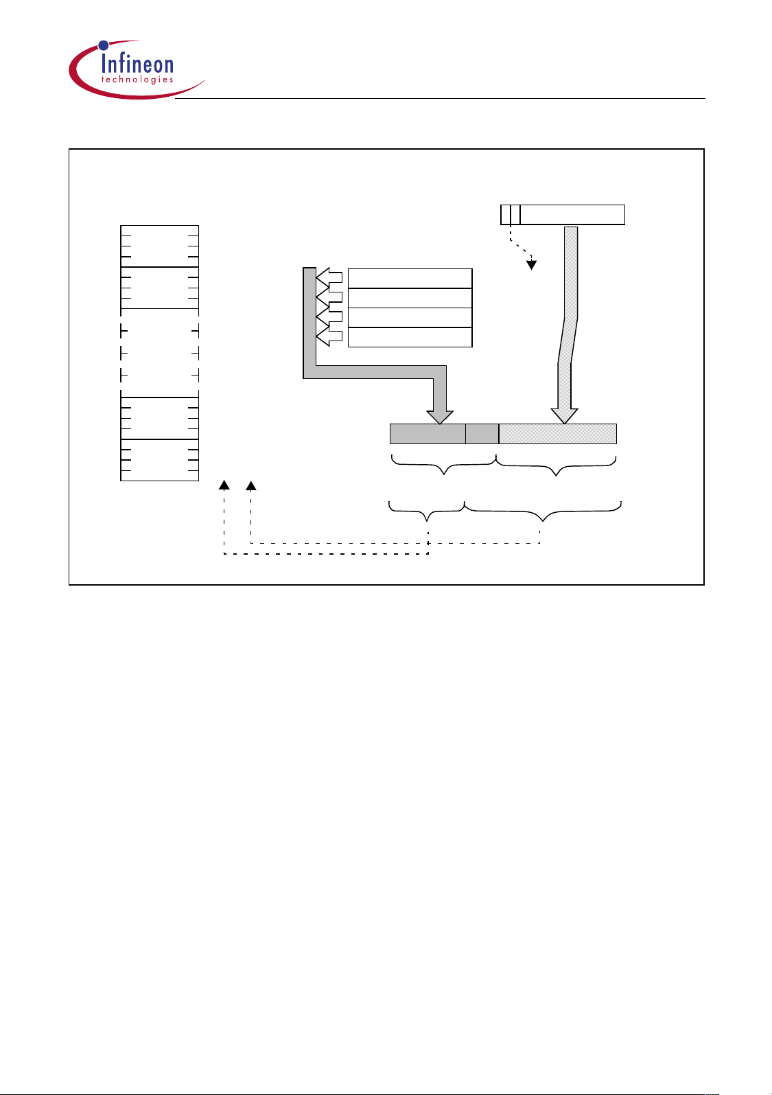
User Manual
C166S V2
Memory
255
09
254
FF’0000
FE’0000
H
H
DPP
Central Processing Unit
16-Bit Data Address (IDXx)
015 14
selects DPP
DPP3 - 11
DPP2 - 10
DPP1 - 01
DPP0 - 00
x
1
01’0000
0
00’0000
H
H
Page
Page offset
023 15 14
Segment Segment offset
Figure 2-18 CoMOV Operations and Addressing via the IDX Pointers
There are indirect addressing modes which allow parallel data move operations before
the long 16-bit address is calculated. Other indirect addressing modes allow
decrementing or incrementing the indirect address pointers (IDXx contents) by 2 or by
the contents of the offset registers. There are two non-bit addressable offset registers
QX0 and QX1 which can be used in conjunction with the CoXXX instructions.
User Manual 2-58 V 1.7, 2001-01

User Manual
C166S V2
Central Processing Unit
The Offset Register QX0 and QX1
These two non-bit addressable registers are used only for CoXXX operations which
access operands using indirect addressing mode. The QX offset registers are used in
conjunction with the IDX pointers.
QX0
Offset Register ESFR Reset Value: 0000
1514131211109876543210
QX 0
rw r
QX1
Offset Register ESFR Reset Value: 0000
1514131211109876543210
QX 0
H
H
rw r
Field Bits Type Description
QX [15:1] rw Modifiable portion of register QXx
Specifies the 16-bit offset address for indirect
addressing modes.
0 [0] r Fixed to 0
Note: During the initialization of the QX registers, instruction flow stalls are possible. For
the proper operation, refer to the Section 4.1.4.
Physical addresses are generated from indirect address pointers IDX via the following
algorithm:
1) Determine the used IDXx pointer
2) An intermediate long address is calculated for the parallel data move opera-
tion of CoXXXM instructions before the long 16-bit address is generated
[optional step!]:
- If required, indirect address pointers (‘IDXx±’) are de/incremented by D=2.
- If required, indirect address pointers (‘IDXx± QXx’) are de/incremented by
D= QXx.
User Manual 2-59 V 1.7, 2001-01

User Manual
C166S V2
Intermediate Address = (IDXx Address) ± D ; [optional step!]
3) Calculate long 16-bit address:
Long Address = (IDXx Pointer)
4) Calculate the physical 24-bit address using the resulting long address and the
corresponding DPP register contents (see long ’mem’ addressing modes and
DPPi override mechanism for arithmetic CoXXX instructions).
Physical Address = (DPPi) + Page offset
5) - If required, indirect address pointers (‘IDXx±’) are in/decremented by D=2 for
word operations.
- If required, indirect address pointers (‘IDXx± QXx’) are in/decremented by
D= QXx for word operations.
Central Processing Unit
(IDX Pointer) = (IDX Pointer) ± D; [optional step!]
The following indirect addressing modes are provided: .
Table 2-8 DSP Addressing Modes
Mnemonic Particularities
[IDXx] Most CoXXX instructions accept IDXx (IDX0, IDX1) as an indirect
address pointer.
[IDXx+] The specified indirect address pointer is automatically post-incremented
by 2 after the access.
with parallel
data move
[IDXx-] The specified indirect address pointer is automatically post-
In case of a CoXXXM instruction, the address stored in the specified
indirect address pointer is automatically pre-decremented by 2 for the
parallel move operation. The pointer itself is not pre-decremented.
Then, the specified indirect address pointer is automatically postincremented by 2 after the access.
decremented by 2 after the access.
User Manual 2-60 V 1.7, 2001-01

User Manual
C166S V2
Table 2-8 DSP Addressing Modes (cont’d)
Mnemonic Particularities
with parallel
data move
[IDXx+QXx] The specified indirect address pointer is automatically post-incremented
with parallel
data move
[IDXx-QXx] The specified indirect address pointer is automatically post-
In case of a CoXXXM instruction, the address stored in the specified
indirect address pointer is automatically pre-incremented by 2 for the
parallel move operation. The pointer itself is not pre-incremented. Then,
the specified indirect address pointer is automatically post-decremented
by 2 after the access.
by QXx after the access.
In case of a CoXXXM instruction, the address stored in the specified
indirect address pointer is automatically pre-decremented by QXx for
the parallel move operation. The pointer itself is not pre-decremented.
Then, the specified indirect address pointer is automatically postincremented by QXx after the access.
decremented by QXx after the access.
Central Processing Unit
with parallel
data move
The example in Figure 2-19 shows the complex operation of CoXXX instructions with a
parallel move operation based on the descriptions about addressing modes given in
Section 2.5.2.4 (Indirect Addressing Modes) and Section 2.5.3 (DSP Addressing
Modes).
In case of a CoXXXM instruction, the address stored in the specified
indirect address pointer is automatically pre-incremented by QXx for the
parallel move operation. The pointer itself is not pre-incremented. Then,
the specified indirect address pointer is automatically post-decremented
by QXx after the access.
User Manual 2-61 V 1.7, 2001-01

User Manual
C166S V2
CoXXXMxx [IDX0+],[R2+]
Address operations
1)
calculate pointer addresses
IDXx = IDX0
2)
intermediate address of write pointer
for the parallel mov operation
Intermediate Address = (IDX0) - 2
3)
calculate long 16bit address
Long Address 1 = (IDX0)
4)
calculate 24bit physical address
Physical Address 1 = Page3 + Page offset
5) post modify address pointer
(IDX0)
= (IDX0) + 2 (R2)
new
Central Processing Unit
R2 Address = CP + 2*2
(global register bank)
Long Address 2 = (R2)
Physical Address 2 = (DPPi) + Page offset
= (R2) + 2
new
Data operations
1)
Read operands
op1 = (Physical Address 1) op2 = (Physical Address 2)
2) Write operand op1
(Intermediate Address) = op1
op1
(IDX0)
(updated pointer)
new
(IDX0) (read pointer)
op2
(R2)
new
(R2) (read pointer)
Intermediate Address
parallel
(write pointer for parallel move)
move
Figure 2-19 Arithmetic MAC Operations with Parallel Move
(updated pointer)
User Manual 2-62 V 1.7, 2001-01
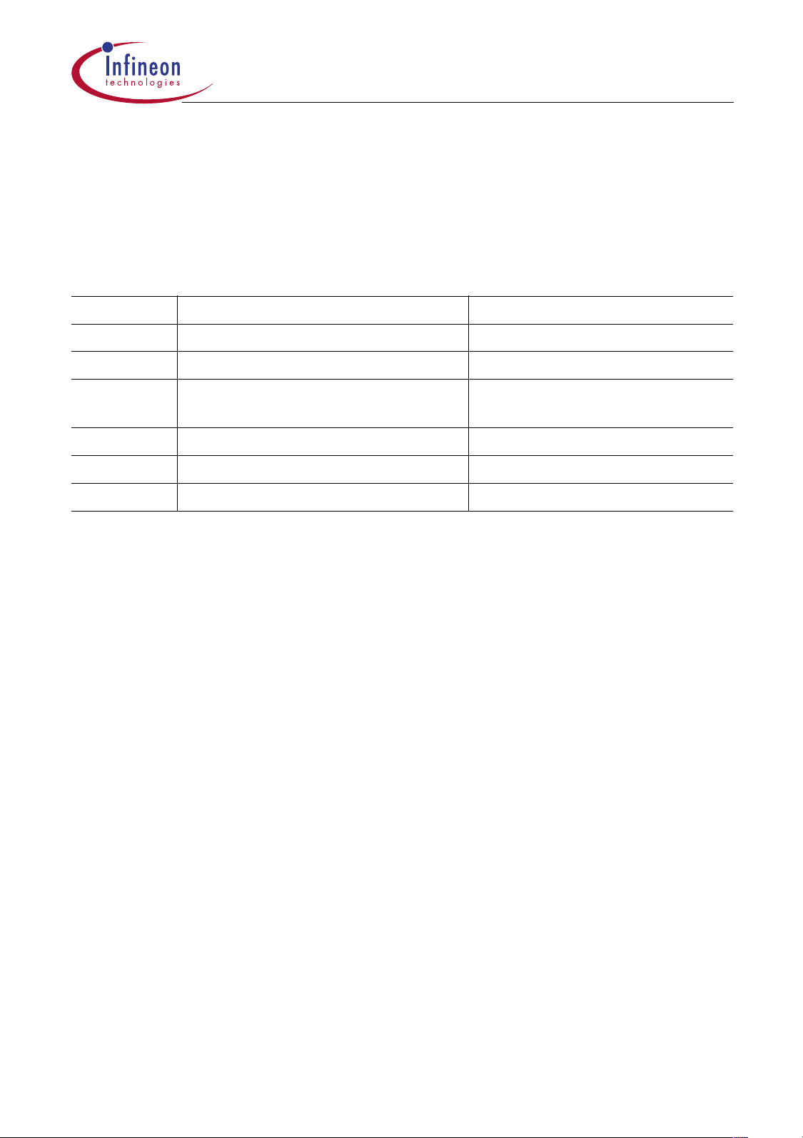
User Manual
C166S V2
Central Processing Unit
2.5.4 The CoREG Addressing Mode
The CoSTORE instruction utilizes the special CoREG addressing mode for immediate
storage of the MAC-Unit register after a MAC operation. The address of the MAC-Unit
register is coded in the CoSTORE instruction format as described in the following table:
.
Table 2-9 Coding of the CoREG Addressing Mode
Mnemonic Register Coding of wwww:w bits [31:27]
MSW MAC-Unit Status Word 00000
MAH MAC-Unit Accumulator High Word 00001
MAS Limited MAC-Unit Accumulator High
Word
MAL MAC-Unit Accumulator Low Word 00100
MCW MAC-Unit Control Word 00101
MRW MAC-Unit Repeat Word 00110
00010
User Manual 2-63 V 1.7, 2001-01

User Manual
C166S V2
Central Processing Unit
2.5.5 The System Stack
The C166S V2 CPU supports a system stack of 64 kBytes. The stack can be located
internally in one of the on-chip memories or externally. The 16-bit Stack Pointer (SP)
register addresses the stack within a 64 kByte segment. The Stack Pointer Segment
Register (SPSG) selects the segment in which the stack is located. A virtual stack
(usually bigger then 64 kBytes) can be implemented by software. This mechanism is
supported by registers STKOV and STKUN (see descriptions below).
The Stack Pointer Register SP
The non-bit addressable Stack Pointer SP register is used to point to the top of the
system stack (TOS). The SP register is pre-decremented whenever data is to be pushed
onto the stack, and it is post-incremented whenever data is to be popped from the stack.
Therefore, the system stack grows from higher toward lower memory locations.
The SP register can be updated via any instruction capable of modifying an 16-bit SFR.
Note: Due to the internal instruction pipeline, a stack pointer initialization stalls the
instruction flow until the operation is finished. A POP and RETURN instruction can
immediately follow an instruction updating the SP.
SP
Stack Pointer SFR Reset Value: FC00
1514131211109876543210
SP 0
rwh r
Field Bits Type Description
SP [15:1] rwh Modifiable portion of register SP
Specifies the top of the system stack.
0 [0] r Fixed to 0
H
User Manual 2-64 V 1.7, 2001-01

User Manual
C166S V2
Central Processing Unit
The Stack Pointer Segment Register SPSEG
This non-bit addressable register selects the segment being used at run-time to access
system stack. The lower eight bits of register SPSEG select one of up 256 segments of
64-kilobytes each, while the higher 8 bits are reserved for future use.
SPSEG
Stack Pointer Segment SFRb Reset Value: 0000
1514131211109876543210
0 0 0 0 0 0 0 SPSEGNR
0
rrrrrrrr rw
Field Bits Type Description
SPSEGNR [7:0] rw Stack Pointer Segment Number
Specifies the segment where the stack is located.
System stack addresses are generated by directly extending the 16-bit contents of the
SP register by the contents of the SPSG register as shown in Figure 2-20.
H
The system stack cannot cross a 64k byte segment boundary.
SPSEG
Stack Pointer Segment
255
FF’0000
254
FE’0000
1
0
01’0000
00’0000
H
H
SPSEGNR
715
H
H
0
16 15
SP
015
023
Figure 2-20 Addressing via the Stack Pointer
In case of a non-segmented memory mode, the SPSG register is also used to generate
the physical address. If a non-segmented memory model is selected, extreme care
should be taken when changing the contents of the SPSG register. Improper SPSG
change may result in erroneous system behavior. The SPSG register can be updated via
any instruction capable of modifying an SFR.
User Manual 2-65 V 1.7, 2001-01

User Manual
C166S V2
Central Processing Unit
Note: Due to the internal instruction pipeline, a write operation to the SPSG register
stalls the instruction flow until the SPSG register is really updated. The instruction
immediately following the instruction updating the SPSG register can use the new
value.
The Stack Overflow Pointer STKOV
This non-bit addressable STKOV register is compared with the SP register before each
implicit write operation which decrements the contents of the SP register. If the contents
of the SP register are equal to the contents of the STKOV register, a stack overflow trap
will occur.
STKOV
Stack Overflow Pointer SFR Reset Value: FA00
1514131211109876543210
STKOV 0
rw r
H
Field Bits Type Description
STKOV [15:1] rw Modifiable portion of register STKOV
Specifies the segment offset address of the lower
limit of the system stack.
0 [0] r Fixed to 0
The STKOV register can be updated via any instruction capable of modifying a SFR.
Note: The Stack Pointer Segment Register SPSG is not taken into account for the stack
pointer comparison. The system stack cannot cross a 64k segment.
This checking mechanism is triggered before every implicit write access. The contents
of the stack pointer is compared with the contents of the overflow register, whenever the
SP is to be decremented either by a CALLA, CALLI, CALLR, CALLS, PCALL, TRAP,
SCXT or PUSH instruction.
Note: If the Stack Pointer was explicitly changed as a result of move or arithmetic
instruction, SP is not compared to the contents of the STKOV. Therefore, if the
modified Stack Pointer is below the limit set by STKOV register, the stack violation
will not be detected. The stack overflow can be detected only if the contents of SP
are equal to (not less than) the contents of the STKOV and only in case of implicit
SP modification. This means that SP may be explicitly set to the value below
permitted SP range and even be operated there without triggering any traps.
However, if SP crosses the limit of the permitted SP range from outside the range
as a result of implicit change (PUSH for example), the event (SP) = (STKOV) will
User Manual 2-66 V 1.7, 2001-01

User Manual
C166S V2
Central Processing Unit
trigger the corresponding trap. Note that event (SP) = (STKOV) resulting from an
explicit SP modification does not trigger the trap.
The Stack Overflow Trap is triggered when (SP) = (STKOV) and if SP is to be implicitly
decremented. This trap may be used in two different ways:
• Fatal error indication treats the stack overflow as a system error and executes
associated trap service routine. Under these circumstances, data in the bottom of the
stack may have been overwritten by the status information stacked upon servicing the
stack overflow trap.
• Automatic system stack flushing allows the system stack to be used as a ’Stack
Cache’ for a bigger external user stack.
The Stack Underflow Pointer STKUN
This non-bit addressable register STKUN is compared with the SP register before each
implicit read operation that increments the contents of the SP register. If the contents of
the SP register are equal to the contents of the STKUN register, a stack underflow
hardware trap will occur.
STKUN
Stack Underflow Pointer SFR Reset Value: FC00
1514131211109876543210
STKUN 0
rw r
Field Bits Type Description
STKUN [15:1] rw Modifiable portion of register STKUN
Specifies the segment offset address of the upper
limit of the system stack.
0 [0] r Fixed to 0
The STKUN register can be updated via any instruction capable of modifying a SFR.
Note: The Stack Pointer Segment Register SPSG is not taken into account for the stack
pointer comparison. The system stack cannot cross a 64 k segment.
This checking mechanism is triggered before each implicit read access. The contents of
the stack pointer are compared to the contents of the underflow register, whenever the
SP will be incremented either by a RET, RETS, RETP, RETI or POP instruction.
H
Note: If the Stack Pointer was explicitly changed as a result of move or arithmetic
instruction, SP is not compared to the contents of the STKUN register. Therefore,
if the modified Stack Pointer is above the limit set by STKUN register, the stack
User Manual 2-67 V 1.7, 2001-01

User Manual
C166S V2
violation will not be detected. The stack underflow can be detected only if the
contents of SP are equal to (not higher than) the contents of the STKUN and only
in case of implicit SP modification. This means that SP may be explicitly set to the
value above the permitted SP range and even be operated there without triggering
any traps. However, if SP crosses the limit of the permitted SP range from outside
the range as a result of an implicit change (POP instruction, for example), the
event (SP) = (STKUN) will trigger the corresponding trap. Note that event (SP) =
(STKUN) resulting from an explicit SP modification does not trigger the trap.
The Stack Underflow Trap is triggered when (SP) = (STKUN) and if SP is to be implicitly
incremented. This trap may be used in two different ways:
Fatal error indication treats the stack underflow as a system error and executes
associated trap service routine.
• Automatic system stack refilling allows use of the system stack as a ’Stack Cache’
for a bigger external user stack.
Scope of Stack Limit Control
The stack limit control implemented by the register pair STKOV and STKUN detects
cases in which the Stack Pointer (SP) crosses the defined stack area as a result of
implicit change.
Central Processing Unit
Note: If a stack overflow or underflow event occurs in an ATOMIC/EXT sequence, the
stack operations that are part of the sequence are completed. The trap is issued
after the completion of the entire ATOMIC/EXT sequence.
2.6 Data Processing
All standard arithmetic, shift and logical operations are performed in the 16-bit ALU. In
addition to the standard arithmetic and logic unit, the ALU of the C166S V2 CPU includes
bit manipulation, multiply and divide unit. Most internal execution blocks have been
optimized to perform operations on either 8-bit or 16-bit numbers. After the pipeline has
been filled, most instructions are completed in one CPU cycle. The status flags are
automatically updated in the PSW register after each ALU operation (see Section 2.6.6).
These flags allow branching upon specific conditions. Support of both signed and
unsigned arithmetic is provided by the user selectable branch test. The status flags are
also preserved automatically by the CPU upon entry into an interrupt or trap routine.
2.6.1 Data Types
The C166S V2 CPU supports operations on booleans/bits, bit strings, characters,
integers, and signed fraction numbers. Most instructions operate with specific data
types, while others are useful for manipulating several data types.
User Manual 2-68 V 1.7, 2001-01

User Manual
C166S V2
The C166S V2 CPU data formats are able to support all ANSI C data types. Additional
to the ANSI C data types, some C-Compilers support new types that allow efficient use
of the bit manipulation instructions in embedded control applications.. .
Table 2-10 ANSI C Data Types
ANSI C Data Types Size (bytes) Range CPU Data Format
bit 1 bit 0 or 1 BIT
sfrbit 1 bit 0 or 1 BIT
esfrbit 1 bit 0 or 1 BIT
signed char 1 -128 to +127 BYTE
unsigned char 1 0 to 255U BYTE
sfr 1 0 to 65535U WORD
esfr 1 0 to 65535U WORD
signed short 2 -32768 to 32767 WORD
unsigned short 2 0 to 65535U WORD
Central Processing Unit
bitword 2 0 to 65535U WORD or BIT
signed int 2 -32768 to 32767 WORD
unsigned int 2 0 to 65535U WORD
signed long 4 -2147483648 to
+2147483647
unsigned long 4 0 to 4294967295UL Not directly supported
float 4 +/-1,176E-38 to
+/-3,402E+38
double 8 +/- 2,225E-308 to
+/- 1,797E+308
long double 8 +/- 2,225E-308 to
+/- 1,797E+308
near pointer 2 16/14 bits
depending on
memory model
far pointer 4 14 bits (16 k) in any
page
Not directly supported
Not directly supported
Not directly supported
Not directly supported
WORD
Not directly supported
User Manual 2-69 V 1.7, 2001-01

User Manual
C166S V2
Central Processing Unit
Table 2-11 CPU Data Formats
CPU Data Format Size (bytes) Range
BIT 1 bit 0 or 1
BYTE 1 0 to 255U or -128 to +127
WORD 2 0 to 65535U or -32768 to 32767
2.6.2 Constants
In addition to the powerful addressing modes, the C166S V2 CPU instruction set also
supports the use of wordwide or bytewide immediate constants. For optimum utilization
of the available code storage, these constants are represented in the instruction formats
by either 3, 4, 8, or 16 bits. The short constants are always zero-extended, while the long
constants are truncated if necessary, to match the data format required for the particular
operation (see table below): .
Table 2-12 Constant Formats
Mnemonic Word Operation Byte Operation
#data3 0000
+ data3 00H + data3
H
#data4 0000H + data4 00H + data4
#data8 0000H + data8 data8
#data16 data16 data16 ∧ FF
H
#mask 0000H + mask mask
Note: Immediate constants are always signified by a leading sign ’#’.
2.6.3 16-bit Adder/Subtracter, Barrel Shifter, and 16-bit Logic Unit
All standard arithmetic and logical operations are performed by the 16-bit ALU. In case
of byte operations, signals from bits 6 and 7 of the ALU result are used to control the
condition flags. Multiple precision arithmetic is supported by a “CARRY-IN” signal to the
ALU from previously calculated portions of the desired operation.
A 16-bit barrel shifter provides multiple bit shifts in a single cycle. Rotations and
arithmetic shifts are also supported.
2.6.4 Bit Manipulation Unit
C166S V2 CPU offers a large number of instructions for bit processing. The special bit
manipulation unit was implemented for this purpose. The bit manipulation instructions
enable efficient control and testing of peripherals. Unlike other microcontrollers,
User Manual 2-70 V 1.7, 2001-01

User Manual
C166S V2
C166S V2 CPU features instructions that provide direct access to two operands in the
bit addressable space without requiring them to be moved to temporary locations.
The same logical instructions that are available for words and bytes can also be used for
bits. The user can compare and modify a control bit for a peripheral in one instruction.
Multiple bit shift instructions have been included to avoid long instruction streams of
single bit shift operations. These instruction require a single CPU cycle. Additionally, bit
field instructions enable are able to modify the multiple bits in one operand in a single
instruction.
All instructions that manipulate single bits or bit groups internally use a read-modify-write
sequence that accesses the whole word containing the specified bit(s).
This method has several consequences:
• Bits can be modified only within the internal address areas, i.e. internal RAM and
SFRs. External locations cannot be used with bit instructions.
The upper 256 bytes of the SFR area, the ESFR area, and the internal RAM are bit
addressable, i.e. those register bits located within the respective sections can be directly
manipulated using bit instructions. The other SFRs must be accessed byte/word wise.
Note: All GPRs are bit addressable independent of the allocation of the register bank via
the Context Pointer (CP). Even GPRs allocated to not bit addressable RAM
locations provide this feature.
Central Processing Unit
• The read-modify-write approach may be critical with hardware-effected bits. In such
cases, the hardware may change specific bits while the read-modify-write operation is
in progress, where the write back would overwrite the new bit value generated by the
hardware. The solution is either the implemented hardware protection (see below) or
realized through special programming (see Section 4.1).
Protected bits are not changed during the read-modify-write sequence, that is, when
hardware sets something like an interrupt request flag between the read and the write of
the read-modify-write sequence. The hardware protection logic guarantees that only the
intended bit(s) is/are effected by the write-back operation.
Note: If a conflict occurs between a bit manipulation generated by hardware and an
intended software access, the software access has priority and determines the
final value of the respective bit.
2.6.5 Multiply and Divide Unit
The C166S V2 CPU multiply and divide unit has two separated parts. One is the fast
16x16-bit multiplier that executes a multiplication in one CPU cycle. The other one is a
division sub-unit which performs the division algorithm in 21 CPU cycles maximum.
According to the data and division types, the division length varies between 18 and 21
cycles. The divide instruction requires four CPU cycles to be executed. For performance
reasons, the rest of the division algorithm runs in the background during the following
User Manual 2-71 V 1.7, 2001-01

User Manual
C166S V2
Central Processing Unit
seventeen CPU cycles, while further instructions are executed in parallel. If another
instruction tries to use the unit while a division is still running, the execution of this new
instruction is stalled until the division is finished.
Interrupt tasks can also be started and executed immediately without any delay. The
previous division will be finished in the background. If an instruction of the interrupt task
uses the multiply and divide unit before the previous division process is finished, the
instruction flow will be stalled as well. To avoid these stalls, the multiply and division unit
should not be used during the first fourteen CPU cycles of the interrupt tasks. This
requires up to fourteen one-cycle instructions to be executed between the interrupt entry
and the first instruction which uses the multiply and divide unit again (worst case).
The Multiply/Divide High Register MDH
The sixteen bit, non-bit addressable MDH register contains the high word of the 32-bit
multiply/divide MD register used by the CPU when it performs a multiplication or a
division using implicit addressing (DIV, DIVL, DIVLU, DIVU, MUL, MULU). After an
implicitly addressed multiplication, this register represents the high order sixteen bits of
the 32-bit result. For long divisions, the MDH register must be loaded with the high order
sixteen bits of the 32-bit dividend before the division has started. After any division, the
MDH register represents the 16-bit remainder.
MDH
Multiply Divide High Word SFR Reset Value: 0000
1514131211109876543210
MDH
rwh
Field Bits Type Description
MDH [15:0] rwh High part of MD
The high order sixteen bits of the 32-bit multiply and
divide register MD.
Whenever this register is updated via software, the Multiply/Divide Register In Use
(MDRIU) flag in the Multiply/Divide Control register (MDC) is set to 1.
The Multiply/Divide Low Register MDL
The sixteen bit, non-bit addressable MDL register contains the low word of the 32-bit
multiply/divide MD register used by the CPU when it performs a multiplication or a
division using implicit addressing (DIV, DIVL, DIVLU, DIVU, MUL, MULU). After a
H
User Manual 2-72 V 1.7, 2001-01

User Manual
C166S V2
Central Processing Unit
multiplication, this register represents the low order sixteen bits of the 32-bit result. For
long divisions, the MDL register must be loaded with the low order sixteen bits of the
32-bit dividend before the division has started. After any division, the MDL register
represents the 16-bit quotient.
MDL
Multiply Divide Low Word SFR Reset Value: 0000
1514131211109876543210
MDL
rwh
Field Bits Type Description
MDL [15:0] rwh Low part of MD
The low order 16 bits of the 32-bit multiply and
divide register MD.
H
Whenever this register is updated via software, the Multiply/Divide Register In Use
(MDRIU) flag in the Multiply/Divide Control register (MDC) is set to 1. The MDRIU flag is
cleared whenever the MDL register is read via software.
The Divide Control Register MDC
This bit addressable 16-bit register is implicitly used by the CPU when it performs a
division or multiplication in the ALU.
MDC
Multiply Divide Control SFRb Reset Value: 0000
1514131211109876543210
0
0 0 0 0 0 0 0 0 0 0
rrrrrrrrrrrrwh rrrr
MDR
IU
0
0 0 0
Field Bits Type Description
MDRIU [4] rwh Multiply/Divide Register In Use
0: Cleared when MDL is read via software.
1: Set when MDL or MDH is written via
software, or when a multiply or divide
instruction is executed.
H
User Manual 2-73 V 1.7, 2001-01

User Manual
C166S V2
Central Processing Unit
The MDRIU flag is the only portion of the MDC register used for multiplication and
division within the C166S V2 CPU. This bit indicates the usage of the MDL and MDH
register. It must be stored prior to a new multiplication or division operation. The
remaining portions of the MDC register are never used by the dedicated multiplication
and division hardware.
2.6.6 The Processor Status Word PSW
This bit addressable register reflects the current status of the microcontroller. Two
groups of bits represent the current ALU status and the current CPU interrupt status.
Two separate bits (USR0 and USR1) within register PSW are provided as general
purpose flags.
PSW
Processor Status Word SFRb Reset Value: 0000
1514131211109876543210
ILVL IEN
HLD
EN
BANK
USR1USR0MUL
IP
EZVCN
H
rwh
rw rw
rwh
rwh r rwh rwh rwh rwh rwh
rwh
Field Bits Type Description
ILVL [15:12] rwh CPU Priority Level
0
Lowest Priority
H
... ...
F
Highest Priority
H
IEN [11] rw Interrupt/PEC Enable Bit (globally)
0 Interrupt/PEC requests are disabled
1 Interrupt/PEC requests are enabled
HLDEN [10] rw Hold Enable
0 external bus arbitration disabled
1 external bus arbitration enabled
BANK [9:8] rwh Reserved for Register File Bank Selection
00 Global register bank
01 Reserved
10 Local register bank 1
11 Local register bank 2
USR1 [7] rwh General Purpose Flag
May be used by application
USR0 [6] rwh General Purpose Flag
May be used by application
User Manual 2-74 V 1.7, 2001-01

User Manual
C166S V2
Central Processing Unit
Field Bits Type Description
MULIP [5] r Multiplication/Division in progress
Always set to 0
E [4] rwh End of Table Flag
0 Source operand is neither 8000h nor 80
1 Source operand is 8000h or 80
Z [3] rwh Zero Flag
0 ALU result is not zero
1 ALU result is zero
V [2] rwh Overflow Flag
0 No Overflow produced
0 Overflow produced
C [1] rwh Carry Flag
0 No carry/borrow bit produced
1 Carry/borrow bit produced
N [0] rwh Negative Result
0 ALU result is not negative
1 ALU result is negative
h
h
ALU Status (N, C, V, Z, E, MULIP)
The condition flags (N, C, V, Z, E) within the PSW indicate the ALU status resulting from
the last performed ALU operation. They are set by the majority of instructions according
to the specific rules depending on the ALU operation or data movement.
After execution of an instruction which explicitly updates the PSW register, the condition
flags may no longer represent an actual CPU status. An explicit write operation to the
PSW register supersedes the condition flag values implicitly generated by the CPU. An
explicit read access to the PSW register returns the value of the PSW register after
execution of the immediately preceding instruction.
Note: After reset, all of the ALU status bits are cleared.
• N-Flag: For the majority of ALU operations, the N-flag is set to 1, if the most significant
bit of the result contains a 1; otherwise, it is cleared. In the case of integer operations,
the N-flag can be interpreted as the sign bit of the result (negative: N = 1, positive: N
= 0). Negative numbers are always represented as the 2s complement of the
corresponding positive number. The range of signed numbers extends from '–8000
H
to '+7FFFH' for the word data type, or from '–80H' to '+7FH' for the byte data type. For
Boolean bit operations with only one operand, the N-flag represents the previous state
of the specified bit. For Boolean bit operations with two operands, the N-flag
represents the logical XORing of the two specified bits.
'
User Manual 2-75 V 1.7, 2001-01

User Manual
C166S V2
Central Processing Unit
• C-Flag: After an addition, the C-flag indicates that a “Carry” from the most significant
bit of the specified word or byte data type has been generated. After a subtraction or
a comparison, the C-flag indicates a “Borrow” which represents the logical negation of
a “Carry” for the addition.
This means that the C-flag is set to 1, if no carry from the most significant bit of the
specified word or byte data type has been generated during a subtraction. Subtraction
is performed by the ALU as a 2s complement addition. The C-flag is cleared when this
complement addition causes a “Carry”.
The C-flag is always cleared for logical, multiply and divide ALU operations, because
these operations cannot cause a “Carry” flag to be set.
For shift and rotate operations, the C-flag represents the value of the bit shifted out
last. If a shift count of zero is specified, the C-flag will be cleared. The C-flag is also
cleared for a Prioritize operation, because a 1 is never shifted out of the MSB during
the normalization of an operand.
For Boolean bit operations with only one operand, the C-flag is always cleared. For
Boolean bit operations with two operands, the C-flag represents the logical ANDing of
the two specified bits.
• V-Flag: The addition, subtraction and 2's complement operations set the V-flag to '1'
if the result exceeds the range of 16 bit signed numbers for word operations ('–8000H'
to '+7FFF
'), or 8 bit signed numbers for byte operations ('–80H' to '+7FH'). Otherwise,
H
the V-flag is cleared. Note, that the result of an integer addition, integer subtraction,
or 2's complement is not valid if the V-flag indicates an arithmetic overflow.
For multiplication and division the V-flag is set to 1 if the result can not be represented
in a word data type, otherwise it is cleared. Note that a division by zero will always
cause an overflow. Unlike the division result, the result of multiplication is valid
regardless of V-flag value.
Since the logical ALU operations cannot produce an invalid result, the V-flag is cleared
by these operations.
The V-flag is also used as 'Sticky Bit' for rotate right and shift right operations. Using
only the C-flag, a rounding error caused by a shift right operation can be estimated as
up to one half of the LSB of the result. In conjunction with the V-flag, the C-flag allows
evaluation of the rounding error with a finer resolution (see table below).
For Boolean bit operations with only one operand, the V-flag is always cleared. For
Boolean bit operations with two operands, the V-flag represents the logical ORing of
the two specified bits.
Shift Right Rounding Error Evaluation
• Z-Flag: The Z-flag is normally set to 1 if the result of an ALU operation equals zero;
otherwise, it is cleared.
User Manual 2-76 V 1.7, 2001-01

User Manual
C166S V2
Central Processing Unit
C-Flag V-Flag Rounding Error Quantity
0
0
1
1
0
1
0 < Rounding error < 1/2 LSB
0
1
No rounding error
Rounding error = 1/2 LSB
1
Rounding error >
/2 LSB
For addition and subtraction with “Carry”, the Z-flag is only set to 1 if the Z-flag already
contains a 1 as a result from previous operation and the result of the current ALU
operation also equals zero. This mechanism supports the multiple precision
calculations.
For Boolean bit operations with only one operand, the Z-flag represents the logical
negation of the previous state of the specified bit. For Boolean bit operations with two
operands, the Z-flag represents the logical NORing of the two specified bits. For the
Prioritize operation, the Z-flag indicates whether the second operand was zero or not.
• E-Flag: End of table flag. The E-flag can be altered by the instructions which perform
ALU or data movement operations. The E-flag is cleared by those instructions that
cannot be reasonably used for table search operations. In all other cases, the E-flag
value depends on the value of the source operand to signify whether the end of a
search table is reached or not. If the value of the source operand of an instruction
equals the lowest negative number which depends on the data format of the
corresponding instruction ('8000H' for the word data type, or '80H' for the byte data
type), the E-flag is set to 1; otherwise, it is cleared.
• MULIP-Flag: The MULIP-flag always sticks to 0.
Note: The MULIP flag is a part of the C166 task environment. For compatibility reasons,
the bit is still implemented even if not used. A multiply and divide ALU operation
of the C166S V2 CPU is no longer interruptible.
• BANK: The BANK bitfield of the PSW registers indicates which one of the three
physical register banks is activated. The BANK field is updated by hardware upon
entry into an interrupt service routine, but it can be also modified by software. The
BANK field can be changed explicitly by any instruction which can write to the PSW.
Also, it is implicitly updated by the RETI instruction.
• HLDEN: Refer to EBC Chapter 6.4.1.
CPU Interrupt Status (IEN, ILVL)
The Interrupt Enable bit allows global enable (IEN=1) or disable (IEN=0) of interrupts.
The 4-bit Interrupt Level field (ILVL) specifies the priority of the current CPU activity. The
interrupt level is updated by hardware upon entry into an interrupt service routine, but it
can also be modified via software to prevent other interrupts from being acknowledged.
In case an interrupt level '15' has been assigned to the CPU, it has the highest possible
User Manual 2-77 V 1.7, 2001-01

User Manual
C166S V2
Central Processing Unit
priority, and thus the current CPU operation cannot be interrupted except by hardware
traps or external non-maskable interrupts. For details please, refer to Section 5
“Interrupt and Trap Functions”.
After reset, all interrupts are globally disabled and the lowest priority (ILVL=0) is
assigned to the initial CPU activity.
2.7 Parallel Data Processing
The new CoXXX arithmetic instructions are performed in the MAC unit. The MAC unit
provides single instruction-cycle, non-pipelined, 32-bit additions; 32-bit subtraction; right
and left shifts; 16-bit by 16-bit multiplication; and multiplication with cumultative
subtraction/addition. The MAC unit includes the following major components, shown in
Figure 2-21:
• 16-bit by 16-bit signed/unsigned multiplier with signed result
• Concatenation Unit
• Scaler (one-bit left shifter) for fractional computing
• 40-bit Adder/Subtracter
• 40-bit Signed Accumulator
• Data Limiter
• Accumulator Shifter
• Repeat Counter
1)
1)
The same hardware-multiplier is used in the ALU.
User Manual 2-78 V 1.7, 2001-01

User Manual
C166S V2
16-bit input operands
Concatenation
Unit
signed/unsigned
Multiplier
Signed
Ext.
40-bit Adder/Subtracter
Round+Saturation
40-bit Signed Accumulator
ACCU-Shifter
Central Processing Unit
Repeat Counter
MCW Register
MSW Register
Limiter
16-bit
32-bit
40-bit
Figure 2-21 Functional MAC Unit Block Diagram
The working register of the MAC Unit is a dedicated 40-bit wide Accumulator register. A
set of consistent flags is automatically updated in the MSW register (see Section 2.7.10)
after each MAC operation. These flags allow branching on specific conditions. Unlike the
PSW flags, these flags are not preserved automatically by the CPU upon entry into an
interrupt or trap routine. All dedicated MAC registers must be saved on the stack if the
MAC unit is shared between different tasks and interrupts.
2.7.1 Representation of Numbers and Rounding
The C166S V2 CPU supports the 2s complement representation of binary numbers. In
this format, the sign bit is the MSB of the binary word. This is set to zero for positive
numbers and set to one for negative numbers. Unsigned numbers are supported only by
multiply/multiply-accumulate instructions which specify whether each operand is signed
or unsigned.
In 2s complement fractional format, the N-bit operand is represented using the 1.[N-1]
format (1 signed bit, N-1 fractional bits). Such a format can represent numbers between
-1 and +1-2
User Manual 2-79 V 1.7, 2001-01
-[N-1]
. This format is supported when MP of MCW is set.
User Manual
C166S V2
Central Processing Unit
The C166S V2 CPU implements 2s complement rounding’. With this rounding type, one
is added to the bit to the right of the rounding point (bit 15 of MAL), before truncation
(MAL is cleared).
2.7.2 The 16-bit by 16-bit signed/unsigned Multiplier and Scaler
The multiplier executes 16-bit by 16-bit parallel signed/unsigned fractional and integer
multiplication in one CPU-cycle. The multiplier allows the multiplication of unsigned and
signed operands. The result is always presented in a signed fractional or integer format.
The result of the multiplication feeds a one-bit Scaler to allow compensation for the extra
sign bit gained in multiplying two 16-bit 2s complement numbers.
2.7.3 Concatenation Unit
The Concatenation Unit enables the MAC unit to perform 32-bit arithmetic operations in
one CPU cycle. The Concatenation Unit concatenates two 16-bit operands to a 32-bit
operand before the 32-bit arithmetic operation is executed in the 40-bit adder/subtracter.
The second required operand is always the current Accumulator contents. The
Concatenation Unit is also used to pre-load the Accumulator with a 32-bit value.
2.7.4 One-bit Scaler
The One-bit scaler can shift the result of the concatenation unit or the output of the
multiplier one bit to the left. The scaler is controlled by the executed instruction for the
concatenation or by the MP control bit.
The product is shifted one bit to the left to compensate for the extra sign bit gained in
multiplying two 16-bit 2s complement numbers. The enabled automatic shift is performed
only if both input operands are signed.
MCW
MAC Control Word SFRb Reset Value: 0000
1514131211109876543210
0
0 0 0 0 MP MS 0 0 0 0 0 0 0 0 0
rrrrrrw rwrrrrrrrrr
Field Bits Type Description
MP [10] rw One-bit scaler control
0 Multiplier product shift disabled
1 Multiplier product shift enabled
H
User Manual 2-80 V 1.7, 2001-01

User Manual
C166S V2
Central Processing Unit
• MP-Control Bit: If the MP mode bit is set and both multiplier operands are signed
types, the multiplier output is automatically shifted left by one bit. In the case of a
multiply and accumulate operation, the output of the multiplier is shifted before being
added to the accumulator.
2.7.5 The 40-bit Adder/Subtracter
The 40-bit adder/Subtracter allows intermediate overflows in a series of multiply/
accumulate operations. The adder/Subtracter has two input ports. The 40-bit port is the
feedback of the Accumulator output through the ACCU-Shifter to the Adder/Subtracter.
The 32-bit port is the input port for the operand coming from the One-bit Scaler. The
32-bit operands are signed and extended to 40-bits before the addition/subtraction is
performed.
The output of the Adder/Subtracter goes to the Accumulator. It is also possible to round
the result and to saturate it on a 32-bit value automatically after every accumulation. The
round operation is performed by adding 00’00008000H to the result. Automatic
saturation is enabled by setting the saturation bit, the MAC Control Word (MCW).
MCW
MAC Control Word SFRb Reset Value: 0000
1514131211109876543210
0 0 0 0 MP MS 0 0 0 0 0 0 0 0 0
0
rrrrrrwrw rrrrrrrrr
Field Bits Type Description
MS [9] rw Saturation control
0 Saturation disabled
1 Saturation enabled
• MS-Control Bit: If the MS mode bit is set, the accumulator will be automatically
saturated to 32-bits. The MAC Unit supports signed saturation.
When the accumulator is in the overflow saturation mode and an overflow occurs, the
accumulator is loaded with either the most positive or the most negative value
representable in a 32-bit value, depending on the direction of the overflow as well as the
arithmetic used. The value of the accumulator upon saturation is 00’7fff’ffffh (positive) or
ff’8000’0000h (negative).
H
2.7.6 The Data Limiter
Saturation arithmetic is also provided to selectively limit overflow when reading the
accumulator by means of a CoSTORE <destination>., MAS instruction. Limiting is
User Manual 2-81 V 1.7, 2001-01

User Manual
C166S V2
Central Processing Unit
performed on the MAC-Unit accumulator. If the contents of the Accumulator can be
represented in the destination operand size without overflow, then the data limiter is
disabled and the operand is not modified. If the contents of the accumulator cannot be
represented without overflow in the destination operand size, the limiter will substitute a
“limited” data as explained in the next table:
Table 2-13 Limiter Output
ME-flag MN-flag Output of Limiter
0 x unchanged
10 7FFF
1 1 8000
H
H
Notice that in this particular case, both the accumulator and the status register are not
affected. MAS is readable by means of a CoSTORE instruction only.
2.7.7 The Accumulator Shifter
The accumulator shifter is a parallel shifter with a 40-bit input and a 40 bit output. The
source accumulator shifting operation are:
• No shift (Unmodified)
• Up to 16-bit Arithmetic Left Shift
• Up to 16-bit Arithmetic Right Shift
Notice that the ME, MSV, and MSL bits from MSW are affected by left shifts; therefore,
if the saturation mechanism is enabled (MS), the behavior is similar to the one of the
Adder/Subtracter.
Note: Certain precautions are required in case of left shift with saturation enabled.
Generally, if MAE contains significant bits, then the 32-bit value in the accumulator
is to be saturated. However, it is possible that left shift may move some significant
bits out of the Accumulator. The 40-bit result will be misinterpreted and will be
either not saturated or saturated incorrectly. There is a chance that the result of
left shift may produce a result which can saturate an original positive number to
the minimum negative value, or vice versa.
2.7.8 The 40-bit Signed Accumulator Register
The 40-bit Accumulator consists of three smaller registers, MAH, MAL, and MAE. MAH
and MAL are 16 bits wide; MAE is 8 bits wide. MAE is the Most Significant Byte of the
40-bit accumulator. This byte performs a guarding function. MAE is accessed as the
Least Significant Byte of MSW.
When MAH is written, the value in the accumulator is automatically adjusted to signed
extended 40-bit format. That means MAE will be automatically loaded by zeros for the
positive number (MAH has 0 in the most significant bit). In the case of the negative
User Manual 2-82 V 1.7, 2001-01

User Manual
C166S V2
Central Processing Unit
number (MAH has 1 in the most significant bit), the MAE will be loaded with ones,
representing the extended 40-bit negative number in 2s compliment notation. One may
see that the extended 40-bit value is equal to 32-bit value without extension. In other
words, after this extension, MAE does not contain significant bits. Generally, this
condition is present when the highest 9 bits of the 40-bit signed result are the same.
During the accumulator operations, an overflow may happen and the result may not fit
into 32-bits and the MAE will change. The extension flag “E”, which is the part of the most
significant byte of MSW, is set when the signed result in the accumulator has overflowed
the 32-bit boundary. This condition is present when the highest 9 bits of the 40-bit signed
result are not the same, i.e. MAE contains significant bits.
Most CoXXX operations specify the 40-bit accumulator register as a source and/or a
destination operand.
The MAC Unit Accumulator Extension Byte MAE
The MAE register is a part of the 40-bit MAC unit accumulator register. MAE is accessed
as the Least Significant Byte of MSW. It is implicitly used by the MAC unit for MAC
operation. In case a word operand is written into MAH, the MAE register becomes signextended. It can be accessed via any instruction capable of accessing an SFR.
MSW
MAC Status Word SFRb Reset Value: 0000
1514131211109876543210
MV MSL ME MSV MC MZ MN MAE
0
rwh rwh rwh rwh rwh rwh rwh rwh
r
Field Bits Type Description
MAE [7:0] rwh The most significant bits of the 40-bit Accumulator
The MAC Unit Accumulator High Word MAH
The MAH register is a part of the 40-bit MAC unit accumulator register. It is implicitly used
by the MAC unit for MAC operation. In case the word operand is written into MAH, MAL
acquires the zero value and the MAE register becomes sign-extended. It can be
accessed via any instruction capable of accessing an SFR.
H
User Manual 2-83 V 1.7, 2001-01

User Manual
C166S V2
Central Processing Unit
MAH
Accumulator High Word SFR Reset Value: 0000
1514131211109876543210
MAH
rwh
Field Bits Type Description
MAH [15:0] rwh High part of Accumulator
The middle (bits 31 to 16) word of the 40-bit MAC
Accumulator.
The MAC Unit Accumulator Low Word MAL
The MAL register is a part of the 40-bit MAC unit accumulator register. It is implicitly used
by the MAC Unit for MAC operation. In case of explicit write access to MAH, MAL
receives a zero value. It can be accessed via any instruction capable of accessing an
SFR.
H
MAL
Accumulator Low Word SFR Reset Value: 0000
1514131211109876543210
MAL
rwh
Field Bits Type Description
MAL [15:0] rwh Low part of Accumulator
The low order 16 bits of the 40-bit MAC
Accumulator.
2.7.9 The Repeat Counter MRW
The Repeat Counter MRW controls the number of repetitions a loop must be executed.
The register must be pre-loaded before it can be used with -USRx CoXXX operations.
MAC operations are able to decrement this counter. When an -USRx CoXXX instruction
is executed, the MRW is checked on the zero value before the MRW is decremented. If
H
User Manual 2-84 V 1.7, 2001-01

User Manual
C166S V2
Central Processing Unit
the MRW equals zero, the USRx bit is set and MRW is not further decremented. The
MRW can be accessed via any instruction capable of accessing a SFR.
MRW
MAC Repeat Word SFRb Reset Value: 0000
1514131211109876543210
REPEAT COUNT
rwh
Field Bits Type Description
REPEAT COUNT [15:0] rwh 16-bit loop counter
All CoXXX instructions have a 3-bit wide repeat control field ’rrr’ in the operand field to
control the MRW repeat counter. It is located within CoXXX instructions at bit positions
[31:29].
–‘000’ -> regular CoXXX instruction.
–‘001’ -> RESERVED
–‘010’ -> ‘- USR0 CoXXX’ instruction, decrements repeat counter.
–‘011’ -> ‘- USR1 CoXXX’ instruction, decrements repeat counter.
–’1xx’ -> RESERVED.
H
The following example shows a loop which is executed 20 times. Every time the
CoMACM instruction is executed, the MRW counter is decremented.
mov MRW, #19
loop01:
- USR1 CoMACM [IDX0+], [R0+]
ADD R2,#2
JMPA cc_nusr1, loop01
Because correctly predicted JMPA is executed in 0-cycle, it offers the functionality of a
repeat instruction.
Note: The USR0 bit should be used carefully because this bit was pre-existing and,
therefore, may have been used by programmer or compiler.
2.7.10 The MAC Unit Status Word MSW
The MSW bit addressable register shows the current MAC Unit state. Two groups of bits
represent the current MAC Unit status and the eight additional extension bits belonging
to the MAC accumulator.
User Manual 2-85 V 1.7, 2001-01

User Manual
C166S V2
Central Processing Unit
MAC Unit Status (MV, MN, MZ, MC, MSV, ME, MSL)
The condition flags (MV, MN, MZ, MC, MSV, ME, MSL) within the MSW indicate the
MAC resulting from the most recently performed MAC operation. These flags are
controlled by the majority of the MAC instructions according to specific rules. Those rules
depend on the instruction managing the MAC or data movement operation.
After execution of an instruction which explicitly updates the MSW register, the condition
flags may no longer represent an actual MAC status. An explicit write operation to the
MSW register supersedes the condition flag values implicitly generated by the MAC unit.
An explicit read access to the MSW register returns the value of the MSW register after
execution of the immediately preceding instruction. The MSW register can be accessed
via any instruction capable of accessing an SFR.
Note: After reset, all MAC status bits are cleared.
MSW
MAC Status Word SFRb Reset Value: 0000
1514131211109876543210
H
0
MV MSL ME MSV MC MZ MN MAE
rwh rwh rwh rwh rwh rwh rwh rwh
r
Field Bits Type Description
MAE [7:0] rwh The most significant bits of the 40-bit Accumulator
MN [8] rwh Negative Result
0 MAC result is positive
1 MAC result is negative
MZ [9] rwh Zero Flag
0 MAC result is not zero
1 MAC result is zero
MC [10] rwh Carry Flag
0 No carry/borrow produced
1 Carry/borrow produced
MSV [11] rwh Sticky Overflow Flag
0 No Overflow occurred
1 Overflow occurred
User Manual 2-86 V 1.7, 2001-01

User Manual
C166S V2
Central Processing Unit
Field Bits Type Description
ME [12] rwh MAC Extension Flag
0 MAE does not contain significant bits
1 MAE contains significant bits
MSL [13] rwh Sticky Limit Flag
0 Result was not saturated
1 Result was saturated
MV [14] rwh Overflow Flag
0 No Overflow produced
1 Overflow produced
• Accu Extension MAE: These 8 bits are part of the 40-bit accumulator register. The
MAC Unit implicitly uses these bits during a MAC operation. When writing to the MAH,
the MAE is automatically signed extended with the most significant bit of the MAH
register.
• MN-Flag: For the majority of the MAC operations, the MN-flag is set to 1 if the most
significant bit of the result contains a 1; otherwise, it is cleared. In the case of integer
operations, the MN-flag can be interpreted as the sign bit of the result (negative:
MN=1, positive: MN=0). Negative numbers are always represented as the 2s
complement of the corresponding positive number. The range of signed numbers
extends from '8000000000
' to '7FFFFFFFFFH'.
H
• MZ-Flag: The MZ-flag is normally set to 1 if the result of a MAC operation equals zero;
otherwise, it is cleared.
• MC-Flag: After a MAC addition, the MC-flag indicates that a “Carry” from the most
significant bit of the accumulator extension MAE has been generated. After a MAC
subtraction or a MAC comparison, the MC-flag indicates a “Borrow” representing the
logical negation of a “Carry” for the addition. This means that the MC-flag is set to 1,
if no “Carry” from the most significant bit of the Accumulator has been generated
during a subtraction. Subtraction is performed by the MAC Unit as a 2s complement
addition and the MC-flag is cleared when this complement addition caused a “Carry”.
For left shift MAC operations, the MC-flag represents the value of the bit shifted out
last. Right shift MAC operations always clear the MC-flag. The arithmetic right shift
MAC operation can set the MC-flag if the enabled round operation generates a “Carry”
from the most significant bit of the Accumulator extension MAE.
• MSV-Flag: The addition, subtraction, 2s complement, and round operations always
set the MSV-flag to 1 if the MAC result overflows the maximum range of 40-bit signed
User Manual 2-87 V 1.7, 2001-01

User Manual
C166S V2
Central Processing Unit
numbers. If the MSV-flag indicates an arithmetic overflow, the MAC result of an
operation is not valid. The MSV-flag is a ’Sticky Bit’. Once set, other MAC operations
cannot affect the status of the MSV-flag. Only a direct write operation can clear the
MSV-flag.
• ME-Flag: The ME-flag is set if the accumulator extension MAE contains significant
bits. The ME-flag is set if the nine highest accumulator bits are not all equal.
• MSL-Flag: The MSL-flag is set if an automatic saturation of the accumulator has
happened. The automatic saturation is enabled if the MS-bit of the MAC Control Word
register MCW is set. The MSL-Flag can be also set by instructions which limit the
contents of the accumulator. If the accumulator has been limited, the MSL-Flag is set.
The MSL-Flag is a 'Sticky Bit'. Once set, it cannot be affected by the other MAC
operations. Only a direct write operation can clear the MSL-flag.
• MV-Flag: The addition, subtraction, and accumulation operations set the MV-flag to 1
if the result exceeds the maximum range of signed numbers (80’00000000H to
7F’FFFFFFFF
); otherwise, the MV-flag is cleared. Note that if the MV-flag indicates
H
an arithmetic overflow, the result of the integer addition, integer subtraction, or
accumulation is not valid.
2.7.11 The MAC Unit Control Word MCW
This bit addressable register controls the operation of the MAC Unit. It can be accessed
via any instruction capable of addressing an SFR.
MCW
MAC Control Word SFRb Reset Value: 0000
1514131211109876543210
0
0 0 0 0 MP MS 0 0 0 0 0 0 0 0 0
rrrrrrw rw rrrrrrrrr
Field Bits Type Description
MP [10] rw One-bit scaler control
0 Multiplier product shift disabled
1 Multiplier product shift enabled
MS [9] rw Saturation control
0 Saturation disabled
1 Saturation enabled
H
User Manual 2-88 V 1.7, 2001-01

User Manual
C166S V2
Central Processing Unit
• MS-Control Bit: If the MS mode bit is set, the accumulator will be automatically
saturated to 32 bits. The MAC Unit supports signed saturation.
• MP-Control Bit: If the MP mode bit is set and both multiplier operands are of signed
types, the multiplier output is automatically shifted left by one bit. In the case of a
multiply and accumulate operation, the output of the multiplier is shifted before being
added to the accumulator.
2.8 Dedicated CSFRs
The Constant Zeros Register ZEROS
All bits of this bit addressable register are fixed to 0 by hardware. This register is readonly. Register ZEROS can be used as a register-addressable constant of all zeros for bit
manipulation or mask generation. It can be accessed via any instruction which is capable
of accessing an SFR.
ZEROS
Constant Zeros Register SFRb Reset Value: 0000
1514131211109876543210
0000000000000000
rrrrrrrrrrrrrrrr
Field Bits Type Description
0 [all] r Fixed to Zero
H
User Manual 2-89 V 1.7, 2001-01

User Manual
C166S V2
Central Processing Unit
The Constant Ones Register ONES
All bits of this bit addressable register are fixed to 1 by hardware. This register is readonly. Register ONES can be used as a register-addressable constant of all ones for bit
manipulation or mask generation. It can be accessed via any instruction capable of
accessing an SFR.
ONES
Constant Ones Register SFRb Reset Value: FFFF
1514131211109876543210
1111111111111111
rrrrrrrrrrrrrrrr
Field Bits Type Description
1 [all] r Fixed to One
H
CPU Identification Register CPUID
This 16-bit register contains the module and revision number of the implemented
C166S V2 core module.
CPUID
CPU Identification Register ESFR Reset Value: 03??
1514131211109876543210
MODULE NUMBER VERSION NUMBER
rr
Field Bits Type Description
MODULE NUMBER [15:8] r Module Number
03
C166S V2 core module number
H
VERSION NUMBER [7:0] r Version Number
Version Number
H
User Manual 2-90 V 1.7, 2001-01

User Manual
C166S V2
C166S V2 Memory Organization
3 C166S V2 Memory Organization
The memory space of the C166S V2 CPU is configured in a “Von Neumann”
architecture. This means that code and data are accessed within the same linear
address space. All of the physically separated memory areas, including internal ROM/
Flash/DRAM (if integrated into a specific derivative), internal RAM, internal Special
Function Register Areas (SFRs and ESFRs), and external memory are mapped into a
single common address space.
The C166S V2 CPU provides a total addressable memory space of 16 MBytes. This
address space is arranged as 256 segments of 64 KBytes each. Each segment is again
subdivided into four data pages of 16 KBytes each (see Figure 3-1).
Most internal memory areas are mirrored into the system segment, segment 0. The
upper 4 KBytes of segment 0 (00’F000
Areas (SFR and ESFR) and the DPRAM areas.
Data may be stored in any part of the internal memory areas. Code may be stored in any
part of the internal memory areas except the SFR blocks, the DPRAM, and Internal
SRAM and internal IO area as these areas may be used for control/data, but not for
instructions.
...00’FFFFH) hold the Special Function Register
H
The 64 KByte memory area of segment 191 (BF’0000
store code and data. It is reserved for “on chip” boot and debug/monitor program
memories.
Accesses to internal memory areas on devices without the appropriate internal
memories will produce unpredictable results.
...BF’FFFFH) cannot be used to
H
User Manual 3-91 V 1.7, 2001-01

User Manual
C166S V2
Segment
FF´FFFF
Data Page 1023
H
C166S V2 Memory Organization
255
FF´0000
H
4MByte
int. program memory
C0´0000
H
Segment
191
reserved
BF´0000
H
RAM /
SFR
8MByte
ext. memory
41´0000
H
Data Page 3
Segment
64
40´0000
H
internal-IO
Area
Internal
SRAM
00’FFFF
00’F000
00’E000
00’C000
H
H
H
H
Internal
21´0000
2MByte
ext. IO
Segment
32
20´0000
03´0000
H
H
H
Data Page 2
Data Page 1
SRAM
00’8000
H
Segment
2
~2 MByte
ext. memory
Segment
02´0000
H
External
Memory
00’4000
H
1
Segment
0
01´0000
Data Page 3
...
H
Data Page 0
Data Page 0
00´0000
H
16MByte
00´0000
H
System Segment 0
64KByte
Figure 3-1 Memory Areas and Address Space
User Manual 3-92 V 1.7, 2001-01

User Manual
C166S V2
C166S V2 Memory Organization
3.1 Data Organization in Memory
Bytes are stored at even or odd byte addresses. Words are stored in ascending memory
locations with the low byte at an even byte address followed by the high byte at the next
odd byte address. Instruction double words are stored in ascending memory locations
as two subsequent words, without any restrictions (non aligned). Single bits are always
stored in the specified bit position at a word address. The memory and registers store
data and instructions in little endian byte order (the least significant bytes are at lower
addresses) The byte ordering is illustrated in Figure 3-2. Bit position 0 is the least
significant bit of the byte at an even byte address, and bit position 15 is the most
significant bit of the byte at the next odd byte address. Bit addressing is supported for a
part of the Special Function Registers, a part of the internal RAM, and for the General
Purpose Registers.
º
11
... Bits ...
Byte
Byte
Word (High Byte)
Word (Low Byte)
Double Word (High)
Double Word (Third)
Double Word (Second)
Double Word (Low Byte)
º
8... Bits ...
067
xxxx’xxxA
xxxx’xxx9
xxxx’xxx8
xxxx’xxx7
xxxx’xxx6
xxxx’xxx5
xxxx’xxx4
xxxx’xxx3
xxxx’xxx2
xxxx’xxx1
xxxx’xxx0
xxxx’xxxF
H
H
H
H
H
H
H
H
H
H
H
H
Figure 3-2 Storage of Words, Bytes and Bits in a Byte Organized Memory
Note: Byte units forming a single word must always be stored within the same physical
(internal, external, ROM, RAM) and organizational (page, segment) memory area.
3.2 Internal Program Memory
The C166S V2 CPU reserves an address area of 4MBytes for Internal Program
Memory. The internal memory can be ROM, SRAM, Flash or DRAM. Devices with
User Manual 3-93 V 1.7, 2001-01

User Manual
C166S V2
Internal Program Memory expand the Internal Program Memory area from the beginning
of segment 192, i.e. starting at address C0’0000H.
The Internal Program Memory can be used for both code (instructions) and data
(constants, tables, etc.) storage.
Code fetches are always made on even word addresses. The highest possible code
storage location in the Internal Program Memory is either xx’xxFEH for single word
instructions, or xx’xxFCH, for double word instructions.
Any word and byte data read access may use the indirect or long 16-bit addressing mode.
There is no short addressing mode for Internal Program Memory operands. Any word
data access is made to an even byte address. Any double word access is made to a
modulo 4 address (even word address). The highest possible word data storage location
in the Internal Program Memory is xxxx’xxFE
xxxx’xxFCH.
The Internal Program Memory is not provided for single bit storage, and therefore is not
bit addressable.
Note: The ‘x’ in the locations above depend on the available Internal Program Memory.
C166S V2 Memory Organization
, the highest double word location
H
3.3 DPRAM, Internal SRAM, and SFR Areas
The C166S V2 CPU differentiates between various internal memory types and internal
peripheral areas. These data memories and the IO/SFR areas are located within data
page 3 and provide fast accesses using one dedicated Data Page Pointer (see Figure 3-
3).
Note: Code access is not possible from the DPRAM, the Internal RAM, or the IO/SFR
areas.
3.3.1 Data Memories
Two dedicated volatile memories are available for data storage:
• The DPRAM can be used for:
– General Purpose Register Banks (GPRs)
– Variable and other data storage, especially for MAC operands
– System Stack (not recommended if Internal SRAM is integrated)
• The Internal SRAM can be used for:
– Variable and other data storage
– System Stack (recommended if Internal SRAM is integrated)
A 3 kByte memory area (00‘F200H...000’FE00H) is reserved for the DPRAM. The upper
256 Bytes of the DPRAM (00’FD00H...00’FDFFH) and the GPRs of the current bank are
provided for single bit storage, and thus are bit addressable (see shaded blocks in
Figure 3-3). Any word or byte data in the DPRAM can be accessed via indirect or long
16-bit addressing modes, if the selected DPP register points to data page 3. Any word
User Manual 3-94 V 1.7, 2001-01

User Manual
C166S V2
C166S V2 Memory Organization
data access is made on an even byte address. The highest possible word data storage
location in the DPRAM is 0000’FDFEH.
A 24 kByte memory area (00‘8000H...000’DFFFH) is reserved for the Internal SRAM. Any
word and byte data in the Internal SRAM can be accessed via indirect or long 16-bit
addressing modes, if the selected DPP register points to data page 3 or data page 2. Any
word data access is made on an even byte address. The highest possible word data
storage location in the Internal SRAM is 0000’DFFEH.
00’FFFF
00’FE00
00’FD00
H
H
H
Data Page 3
RAM/SFR
Area
IO
Area
Intenal
SRAM
00’FFFF
00’F000
00’E000
00’C000
H
H
H
internal
IO
SFR
Area
DPRAM
H
Data Page 2
Data Page 1
Data Page 0
Intenal
SRAM
External
Memory
System Segment 0
64KByte
00’8000
00’4000
00´0000
H
DPRAM
H
00’F200
H
ESFR
Area
H
00’F000
H
Figure 3-3 RAM and SFR Areas
User Manual 3-95 V 1.7, 2001-01

User Manual
C166S V2
C166S V2 Memory Organization
3.3.2 Special Function Register Areas
The functions of the CPU, the bus interface, the IO ports, and the on-chip peripherals of
the C166S V2 device are controlled via a number of so-called Special Function
Registers (SFRs). These SFRs are arranged within two areas of 512 Bytes each. The
first register block, the SFR area, is located in the 512 Bytes above the DPRAM
(00’FE00H...00’FFFFH). The second register block, the Extended SFR (ESFR) area, is
located in the 512 Bytes below the DPRAM (00’F000H...00’F1FFH).
Special Function Registers can be addressed via indirect and long 16-bit addressing
modes. Using an 8-bit offset together with an implicit base address allows word SFRs
and their respective low bytes to be addressed. However, this does not work for the
respective high bytes!
Note: High byte access of SFRs using the 8-bit offset addressing mode is not possible.
Note: Writing to any byte of an SFR causes the non-addressed complementary byte to
be cleared!
Note: GPRs can be accessed using the 8-bit offset addressing mode, but they are not
mapped into the SFR and ESFR memory area. an internal peripheral bus access
is executed using the respective long address instead of a GPR access.
The upper half of each register block (except the 16 highest words, refer to Section 2.5.1
) is bit-addressable, so the respective control/status bits can be directly modified or
checked using bit addressing.
When accessing registers in the ESFR area using 8-bit addresses or direct bit
addressing, the Extend Register (EXTR) instruction is required to switch the short
addressing mechanism from the standard SFR area to the Extended SFR area before
accessing registers in the ESFR area. This is not required for 16-bit and indirect
addresses. GPRs R15...R0 are duplicated, i.e. they are accessible within both register
blocks via short 2-, 4- or 8-bit addresses without switching.
Example:
EXTR #4 ;Switch to ESFR area for the next four instructions
MOV ODP2, #data16 ;ODP2 (ESFR register) uses 8-bit register addressing
BFLDL DP6, #mask, #data8;DP6 (ESFR register) bit addressing for bit fields
BSET DP6.7 ;DP6 (ESFR register) bit addressing for single bits
MOV T8REL, R1 ;T8REL uses 16-bit address, R1 is duplicatedº
;...and also accessible via the ESFR mode
;(EXTR is not required for this access)
;------- ;------------------- ;The scope of the EXTR #4 instruction ends here!
MOV T8REL, R1 ;T8REL uses 16-bit address, R1 is duplicatedº
;...and does not require switching
User Manual 3-96 V 1.7, 2001-01

User Manual
C166S V2
C166S V2 Memory Organization
To minimize the switching of SFR banks, the ESFR area contains registers that are
mainly required for initialization and mode selection. Registers that need to be accessed
frequently are allocated to the standard SFR area wherever possible.
Note: The tools are equipped to monitor accesses to the ESFR area and will
automatically insert EXTR instructions, switch the SFR bank address, or issue a
warning in case of missing or excessive EXTR instructions.
3.3.3 IO Area
Some parts of the C166S V2 CPU memory area are marked as IO. These memory areas
have the following special properties:
– Accesses are not buffered and cached
The write back buffers and caches of the C166S V2 CPU are not used to store IO
read and write accesses.
– Special handling of destructive reads
The pipeline of the C166S V2 CPU allows speculative reads. Memory locations of
the IO area are not read until all speculations are solved. Destructive read accesses
are delayed.
– Write before read execution
The pipeline length of the C166S V2 CPU enables a read instruction to read a
memory location before a preceding write instruction has executed its write access.
Data forwarding guarantees the correct instruction flow execution. In case of an IO
read access, the read access will be delayed until all IO writes pending in the
pipeline are executed. In case of a write access, peripherals will change their
internal states. Write accesses must actually be executed before the next read
access is initiated.
Note: The bit manipulation instructions (BSET, BCLR...) use the read-modify-write
approach. The IO read access of this instructions will be stalled until all IO write
accesses are finished.
The following memory areas are marked as IO:
– 2 Mbytes of external IO located to 20’0000H to 3F’FFFF
H
– SFR and ESFR areas located from 00’FE00H to 00’FFFFH and from 00’F000H to
00’F1FFH respectively
– 4 kByte internal IO located from 00’E000H to 00’EFFF
H
Note: All external IO areas support real byte accesses. All internal IO areas do not
support real byte transfers. For more details on the exception of (E)SFR areas
refer to Section 3.3.2.
3.3.4 PEC Source and Destination Pointers
The source and destination pointers for data transfers on the PEC channels are located
in the 4-kByte internal IO area. Each channel uses a pair of pointers stored in two
User Manual 3-97 V 1.7, 2001-01

User Manual
C166S V2
subsequent word registers, with the source pointer (SRCPx) on the lower and the
destination pointer (DSTPx) on the higher word address (x = channel number). The PEC
registers are part of the PEC itself and are addressed via the internal peripheral bus.
In contrast to the C166 family, the pointers are not located in the internal RAM. The
pointers are located in the 4 kByte internal IO.
If a PEC channel is not used, the corresponding pointer locations are not available and
cannot be used for word and byte storage.
Writing to any byte of the PEC pointers does cause the non-addressed complementary
byte to be cleared!
For more detail about use of the source and destination pointers for PEC data transfer,
see the “Interrupt and Exception Execution” section.
C166S V2 Memory Organization
3.4 External Memory Space
The C166S V2 CPU is capable of using an address space of up to 16 MBytes. Only
portions of this address space are occupied by internal memory areas. All addresses not
used for on-chip memory or for registers may reference external memory locations. This
external memory is accessed via the external bus interface. This interface may further
limit the amount of addressable external memory.
External word and byte data can be accessed only via indirect or long 16-bit addressing
modes using one of the four DPP registers. There is no short addressing mode for
external operands. Any word data access is made to an even byte address and double
word accesses to modulo 4 byte addresses (even word address).
The external memory is not provided for single bit storage and therefore is not bit
addressable.
3.4.1 Boot and Debug/Monitor Program Memories
The 64 KByte memory area of segment 191 (BF’0000H...BF’FFFFH) is reserved for boot
and debug/monitor program memories. These “on chip” memories are accessed using
the EBC and are a part of the EBC‘s external memory space. Accesses are not visible
at the port pins of the EBC even if these memories are part of the external memory
space. During normal code execution, this segment is not accessible for the C166S V2
CPU. In case of a read access, the EBC will deliver the predefined 0000H value and write
access will not be executed. Only in special boot and emulation modes can the
memories of segment 191 be accessed.
Note: Segment 191 (BF’0000H...BF’FFFFH) is not usable for the system application.
External memories and peripherals located in this segment will never be
accessed.
User Manual 3-98 V 1.7, 2001-01

User Manual
C166S V2
C166S V2 Memory Organization
3.5 Crossing Memory Boundaries
The address space of the C166S V2 CPU is implicitly divided into logical memory areas
and equally sized blocks of different granularity. Crossing the boundaries between these
areas or blocks (code or data) requires special attention to ensure that the controller
executes the desired operations.
Memory Areas are partitions of the address space that represent different kinds of
memory (if provided at all). These memory areas are the internal RAM areas, the internal
IO areas, the internal Program Memories (if available), and the external memory.
Accessing subsequent data locations that belong to different memory areas is not fully
supported and may therefore lead to erroneous results. There is no problem if the
memory boundaries are word aligned. However, when executing code, the different
memory areas (Internal Program Memory areas and external memory) must be switched
explicitly via branch instructions. Sequential boundary crossing is not supported and may
leads to erroneous results.
Segments are contiguous blocks of 64 KBytes each. They are referenced via the Code
Segment Pointer (CSP) for code fetches and via an explicit segment number for data
accesses overriding the standard DPP scheme.
During code fetching, segments are not changed automatically, but rather must be
switched explicitly. The instructions JMPS, CALLS, and RETS will do this. Larger
sequential programs make sure that the highest used code location of a segment
contains an unconditional branch instruction to the respective following segment, to
prevent the prefetcher from trying to leave the current segment.
Data Pages are contiguous blocks of 16 KBytes each. They are referenced via the data
page pointers DPP3...0 and via an explicit data page number for data accesses
overriding the standard DPP scheme. Each DPP register can select one of the possible
1024 data pages. The DPP register that is used for the current access is selected via the
two upper bits of the 16-bit data address. Subsequent 16-bit data addresses that cross
the 16 KByte data page boundaries will use different data page pointers, while the
physical locations need not be subsequent within memory.
3.6 System Stack
The system stack may be defined within the internal RAM, but can be also located
externally. The size of the system stack is limited to 64 kBytes and must be located in
one segment. For all system stack operations, the stack memory is accessed via a 24 bit
stack pointer. The Stack Pointer register (SP) represents the low order 16 bits of the
24 bit stack pointer, also referred to as Stack Pointer Offset. The Stack Segment Pointer
(SPSEG) represents the high order 8 bits of the stack pointer, also referred to as Stack
Segment.
The system stack implementation in the C166S V2 CPU is from high to low memory. The
system stack grows downward as it is filled. The SP register is decremented first each
User Manual 3-99 V 1.7, 2001-01

User Manual
C166S V2
time data is pushed on the system stack, and incremented after each time the data is
pulled from the system stack. Only word accesses are supported to the system stack.
The 24 bit stack pointer points to the address of the latest system stack entry, rather than
to the next available system stack address.
A stack overflow (STKOV) register and a Stack Underflow (STKUN) register are
provided to control the lower and upper limits of the selected stack area. These two stack
boundary registers can be used for protection against data destruction.
C166S V2 Memory Organization
3.6.1 Data Organization in Global General Purpose Registers
The C166S V2 CPU differentiates between global memory mapped General Purpose
Register (GPR) banks and local not mapped GPR banks. In addition to the memory
mapped register banks, the C166S V2 CPU has two local not memory mapped GPR
register banks for very fast context switching (see Section 2.4).
Note: The local GPR banks are not memory mapped and the GPRs cannot be accessed
using a long or indirect memory address.
The C166S V2 CPU supports register bank (context) switching. Multiple global memory
mapped register banks can physically exist within the DPRAM at the same time;
however, only the global register bank selected by the Context Pointer register (CP) is
active at a given time. Selecting a new active global register bank is done by simply
updating the CP register.
User Manual 3-100 V 1.7, 2001-01
 Loading...