

Page 1

Microcontrollers
XMC4000/1000
Microcontroller Series
for Industrial Applications
Application Guide
V1.0 2015-01
Introduction to Digital Power
Conversion
Page 2

Edition 2015-01
Published by
Infineon Technologies AG
81726 Munich, Germany
© 2015 Infineon Technologies AG
All Rights Reserved.
Legal Disclaimer
The information given in this document shall in no event be regarded as a guarantee of conditions or
characteristics. With respect to any examples or hints given herein, any typical values stated herein and/or any
information regarding the application of the device, Infineon Technologies hereby disclaims any and all
warranties and liabilities of any kind, including without limitation, warranties of non-infringement of intellectual
property rights of any third party.
Information
For further information on technology, delivery terms and conditions and prices, please contact the nearest
Infineon Technologies Office (www.infineon.com).
Warnings
Due to technical requirements, components may contain dangerous substances. For information on the types in
question, please contact the nearest Infineon Technologies Office.
Infineon Technologies components may be used in life-support devices or systems only with the express written
approval of Infineon Technologies, if a failure of such components can reasonably be expected to cause the
failure of that life-support device or system or to affect the safety or effectiveness of that device or system. Life
support devices or systems are intended to be implanted in the human body or to support and/or maintain and
sustain and/or protect human life. If they fail, it is reasonable to assume that the health of the user or other
persons may be endangered.
Page 3

Introduction to Digital Power Conversion
Revision History
Page or Item
Subjects (major changes since previous revision)
V1.0, 2015-01
XMC4000/1000 Family
Revision History
Trademarks of Infineon Technologies AG
AURIX™, C166™, CanPAK™, CIPOS™, CIPURSE™, CoolMOS™, CoolSET™,
CORECONTROL™, CROSSAVE™, DAVE™, EasyPIM™, EconoBRIDGE™, EconoDUAL™,
EconoPIM™, EiceDRIVER™, eupec™, FCOS™, HITFET™, HybridPACK™, I²RF™, ISOFACE™,
IsoPACK™, MIPAQ™, ModSTACK™, my-d™, NovalithIC™, OptiMOS™, ORIGA™, PRIMARION™,
PrimePACK™, PrimeSTACK™, PRO-SIL™, PROFET™, RASIC™, ReverSave™, SatRIC™,
SIEGET™, SINDRION™, SIPMOS™, SmartLEWIS™, SOLID FLASH™, TEMPFET™, thinQ!™,
TRENCHSTOP™, TriCore™.
Other Trademarks
Advance Design System™ (ADS) of Agilent Technologies, AMBA™, ARM™, MULTI-ICE™, KEIL™,
PRIMECELL™, REALVIEW™, THUMB™, µVision™ of ARM Limited, UK. AUTOSAR™ is licensed by
AUTOSAR development partnership. Bluetooth™ of Bluetooth SIG Inc. CAT-iq™ of DECT Forum.
COLOSSUS™, FirstGPS™ of Trimble Navigation Ltd. EMV™ of EMVCo, LLC (Visa Holdings Inc.).
EPCOS™ of Epcos AG. FLEXGO™ of Microsoft Corporation. FlexRay™ is licensed by FlexRay
Consortium. HYPERTERMINAL™ of Hilgraeve Incorporated. IEC™ of Commission Electrotechnique
Internationale. IrDA™ of Infrared Data Association Corporation. ISO™ of INTERNATIONAL
ORGANIZATION FOR STANDARDIZATION. MATLAB™ of MathWorks, Inc. MAXIM™ of Maxim
Integrated Products, Inc. MICROTEC™, NUCLEUS™ of Mentor Graphics Corporation. Mifare™ of
NXP. MIPI™ of MIPI Alliance, Inc. MIPS™ of MIPS Technologies, Inc., USA. muRata™ of MURATA
MANUFACTURING CO., MICROWAVE OFFICE™ (MWO) of Applied Wave Research Inc.,
OmniVision™ of OmniVision Technologies, Inc. Openwave™ Openwave Systems Inc. RED HAT™
Red Hat, Inc. RFMD™ RF Micro Devices, Inc. SIRIUS™ of Sirius Satellite Radio Inc. SOLARIS™ of
Sun Microsystems, Inc. SPANSION™ of Spansion LLC Ltd. Symbian™ of Symbian Software Limited.
TAIYO YUDEN™ of Taiyo Yuden Co. TEAKLITE™ of CEVA, Inc. TEKTRONIX™ of Tektronix Inc.
TOKO™ of TOKO KABUSHIKI KAISHA TA. UNIX™ of X/Open Company Limited. VERILOG™,
PALLADIUM™ of Cadence Design Systems, Inc. VLYNQ™ of Texas Instruments Incorporated.
VXWORKS™, WIND RIVER™ of WIND RIVER SYSTEMS, INC. ZETEX™ of Diodes Zetex Limited.
Last Trademarks Update 2011-02-24
Page 4

Introduction to Digital Power Conversion
XMC4000/1000 Family
Table of Contents
Table of Contents
1 About this document ......................................................................................................................... 6
1.1 Scope and Purpose .............................................................................................................................. 6
1.2 Intendend Audience ............................................................................................................................. 6
2 Comparison of Power Conversion Methods ................................................................................... 7
2.1 What is Power Conversion ................................................................................................................... 7
2.2 Why Power Conversion ........................................................................................................................ 7
2.3 Methods of Power Conversion ............................................................................................................. 7
2.3.1 Linear Mode Power Conversion ..................................................................................................... 7
2.3.2 Switch Mode Power Conversion .................................................................................................... 9
2.3.2.1 Analog Switch Mode Controllers ............................................................................................. 11
2.3.2.2 Digital Switch Mode Controllers .............................................................................................. 11
2.3.2.3 ASIC controller versus MCU / DSP / DSC controllers ............................................................ 12
2.4 Infineon XMC-families for Switch Mode Power Control ..................................................................... 13
2.4.1 Power Conversion Oriented Peripheral Features ........................................................................ 14
2.4.1.1 Sensing ................................................................................................................................... 14
2.4.1.2 Stability and Software ............................................................................................................. 14
2.4.1.3 Modulation .............................................................................................................................. 14
2.4.1.4 PWM Generation .................................................................................................................... 15
3 Converter Topologies ...................................................................................................................... 16
3.1 Buck ................................................................................................................................................... 17
3.2 Boost .................................................................................................................................................. 18
3.3 PFC .................................................................................................................................................... 19
3.4 Phase-Shift Full-Bridge (PSFB) ......................................................................................................... 21
3.5 LLC (Inductor-Inductor-Capacitor) ..................................................................................................... 22
3.6 Generic Digital Power Converter ........................................................................................................ 23
4 PWM Generation............................................................................................................................... 24
4.1 Single Channel ................................................................................................................................... 24
4.2 Single Channel with Complementary Outputs ................................................................................... 24
4.3 Dual Channel with Complementary Outputs with Dead-Time, using CCU8 ...................................... 25
4.4 Dual Channel with Complementary Outputs with Dead-Time, using CCU4 ...................................... 25
4.5 ON/OFF Control ................................................................................................................................. 27
4.6 Fixed ON-Time (FOT) ........................................................................................................................ 27
4.7 Fixed ON-Time with Frequency Limit Control .................................................................................... 28
4.8 Fixed Off-Time (FOFFT) .................................................................................................................... 31
4.9 Phase Shift Control ............................................................................................................................ 32
4.10 Fixed Phase-Shift ............................................................................................................................... 32
4.10.1 Center Aligned Mode ................................................................................................................... 32
4.10.2 Edge Aligned Mode ...................................................................................................................... 33
4.10.3 Interleave ..................................................................................................................................... 34
4.11 Variable Phase-Shift .......................................................................................................................... 35
4.11.1 Power Conversion Control Example ............................................................................................ 37
4.11.2 Zero-Voltage Switching (ZVS) Control ......................................................................................... 38
4.12 Adding High Resolution Channel (HRC) – HRPWM .......................................................................... 39
4.12.1 PWM Dead-Time Compensation ................................................................................................. 40
4.13 Half-Bridge LLC Control using ½ CCU4............................................................................................. 41
4.14 Half-Bridge LLC Control - Synchronous Rectification using CCU4 ................................................... 42
4.15 Full-Bridge LLC Control Using HRC – Synchronous Rectification ..................................................... 43
4.16 Full-Bridge LLC Control – Synchronous Rectification Using HRC ..................................................... 44
5 Sensing ............................................................................................................................................. 46
5.1 Analog Signal Sensing ....................................................................................................................... 46
5.1.1 Level Crossing Detection, Fast Compare mode .......................................................................... 46
5.1.2 PWM with Fast Compare mode Hysteretic Switching ................................................................. 47
5.1.3 Peak Control Using Fast Compare mode .................................................................................... 48
5.1.4 ZCD Control Using Fast Compare mode ..................................................................................... 49
Application Guide 4 V1.0, 2015-01
Page 5

Introduction to Digital Power Conversion
XMC4000/1000 Family
Table of Contents
5.2 Over Voltage and Over Current Protection (OVP / OCP) .................................................................. 50
6 Modulation ........................................................................................................................................ 51
6.1 Voltage Control (VC) .......................................................................................................................... 52
6.1.1 Timing Scheme ............................................................................................................................ 53
6.2 Current Control ................................................................................................................................... 55
6.2.1 Average Current Control (ACC) ................................................................................................... 55
6.2.2 Average Current Control, Edge-Aligned Scheme ........................................................................ 56
6.2.3 Discontinuous to Continuous Current Recovery by Timer-Load ................................................. 58
6.2.4 ACC Center Aligned Scheme ...................................................................................................... 59
6.3 Peak Current Control (PCC) .............................................................................................................. 60
6.3.1 PCC Timing Scheme.................................................................................................................... 62
6.4 Blanking, Filtering and Clamping ....................................................................................................... 63
6.5 Slope Compensation .......................................................................................................................... 64
6.5.1 A Necessity in Fixed Frequency PCC .......................................................................................... 64
6.5.2 Fast Average Current Mode PCC ................................................................................................ 65
6.5.3 VIN independent Average Current mode ...................................................................................... 66
6.5.4 Slope Compensation Conditions – PCC ...................................................................................... 67
6.5.5 Slope Compensation Conditions: PCC ‘Stable Area’ examples .................................................. 70
6.5.6 Without Slope Compensation, Fixed-ON-Time (FOT) ZCD Control ............................................ 71
6.5.7 Without Slope Compensation, Fixed-OFF-Time (FOFFT) PCC .................................................. 71
6.6 CCM, CRM (CrCM) and DCM ............................................................................................................ 72
6.7 CRM: PFC using Fixed-On-Time (FOT)............................................................................................. 74
6.8 CCM / (DCM): PFC using Fixed-Off-Time (FOFFT) .......................................................................... 75
6.9 CCM: PFC example using Average Current Mode Control ............................................................... 76
7 Control Loops ................................................................................................................................... 77
7.1 Using CSG (HRPWM) with an Internal Comparator and Slope Generator........................................ 77
7.2 Using embedded ACMP and external Slope Compensation Ramp .................................................. 78
7.3 Using FADC Compare Mode; Slope Compensation Add-On ............................................................ 81
7.4 Open Loop Gain Stabilization (Frequency Compensation)................................................................ 83
7.4.1 Open Loop Gain Voltage Mode ................................................................................................... 84
7.4.2 Open Loop Gain Bode Plot, Voltage Mode Stabilization ............................................................. 85
7.4.3 Open Loop Gain Current Mode w/ Slope Compensation ............................................................ 86
7.4.4 Open Loop Gain Bode Plot, Current Mode Stabilization ............................................................. 87
8 Application Software ....................................................................................................................... 88
8.1 Advanced Algorithms / User software IP for Power Conversion ........................................................ 88
8.2 Multi-stage, multi-functional, multi-tasking control by a single controller ........................................... 88
8.3 Safety ................................................................................................................................................. 89
8.4 Communication capabilities ............................................................................................................... 89
8.5 Data logging / Firmware updates ....................................................................................................... 89
8.6 Human Machine Interface .................................................................................................................. 89
8.7 Digital Switch Mode Control by New Feed-Forward Techniques ...................................................... 90
8.8 Non-linear Slope Compensation ........................................................................................................ 90
Application Guide 5 V1.0, 2015-01
Page 6

Introduction to Digital Power Conversion
XMC4000/1000 Family
About this document
1 About this document
1.1 Scope and Purpose
This document aims to stimulate and challenge accepted solutions in the field of power applications
with digital control, by revisiting the basics of electric energy transfer and creating a summarized
picture of what can be achieved today with a weighted mix of embedded dedicated peripherals and
computing power.
1.2 Intendend Audience
The information is intended for persons in charge or executive position, with a diverse background in
the subject – as well as to people with deeply rooted experience in the field, such as power supply
designers, for which we want to show the possibilities XMC families can offer.
Application Guide 6 V1.0, 2015-01
Page 7

Introduction to Digital Power Conversion
Category
Type
General Purpose
DC / DC
DC-to-DC converter
Regulator / Stabilizer / Voltage Adapter
AC / DC
AC-to-DC converter
Rectifier / Mains Power Supply Unit (PSU)
DC / AC
AC-to-DC converter
Inverter
AC / AC
AC-to-AC converter
Transformer / Variable frequency Converter
XMC4000/1000 Family
Comparison of Power Conversion Methods
2 Comparison of Power Conversion Methods
2.1 What is Power Conversion
Power conversion is the conversion of electric energy from one form to another. As long as it does not
concern electro-mechanic equivalent energy that consumes energy (e.g. motors) or produces energy
(e.g. generators), then it is about pure power transfer, in any form, from the following categories:
Table 1 Power conversion categories
2.2 Why Power Conversion
According to the global environmental context, each case of electric energy transfer between an
energy source and an energy consuming unit, should consume as little energy as possible to perform
the task by optimal adaption. This is generally unachievable without some form of power conversion.
2.3 Methods of Power Conversion
There are two significantly different ways to convert a DC supply voltage to another DC voltage:
Linear Power Conversion
Switch Mode Power Conversion
When Switch Mode is chosen (e.g. for High Power) the next choice is between:
Analog (discrete) control
Digital (ASIC/MCU/DSP) control
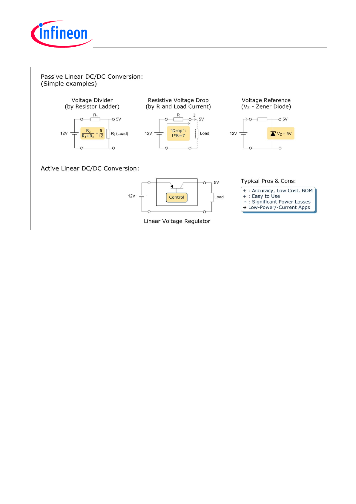
2.3.1 Linear Mode Power Conversion
A Linear DC/DC Converter output/input voltage ratio is < 1 and the output/input current ratio is < 1, so
there is always a significant power loss.
Linear voltage regulators meet such demands as ‘Easy-to-Use’, Accuracy, Low Cost and EMC. They
are therefore the “best-choice” in low power / low current DC-converters.
Application Guide 7 V1.0, 2015-01
Page 8
Introduction to Digital Power Conversion
XMC4000/1000 Family
Comparison of Power Conversion Methods
Figure 1 Linear DC/DC Conversion
Passive Linear Conversion
Passive conversion means that there are no control components involved in the process that are
capable of changing the conversion properties in any way; i.e. the steady state input-to-output transfer
function is not adjustable in runtime. The consequence of this is Load dependent output voltage.
Active Linear Conversion
By “active” conversion we mean that there are components involved that are capable of influencing
the conversion activity; i.e. there is at least one semiconductor capable of controlling the conversion
by at least one additional input signal. This might be to stabilize the output to a reference level for
example.
Application Guide 8 V1.0, 2015-01
Page 9
Introduction to Digital Power Conversion
XMC4000/1000 Family
Comparison of Power Conversion Methods
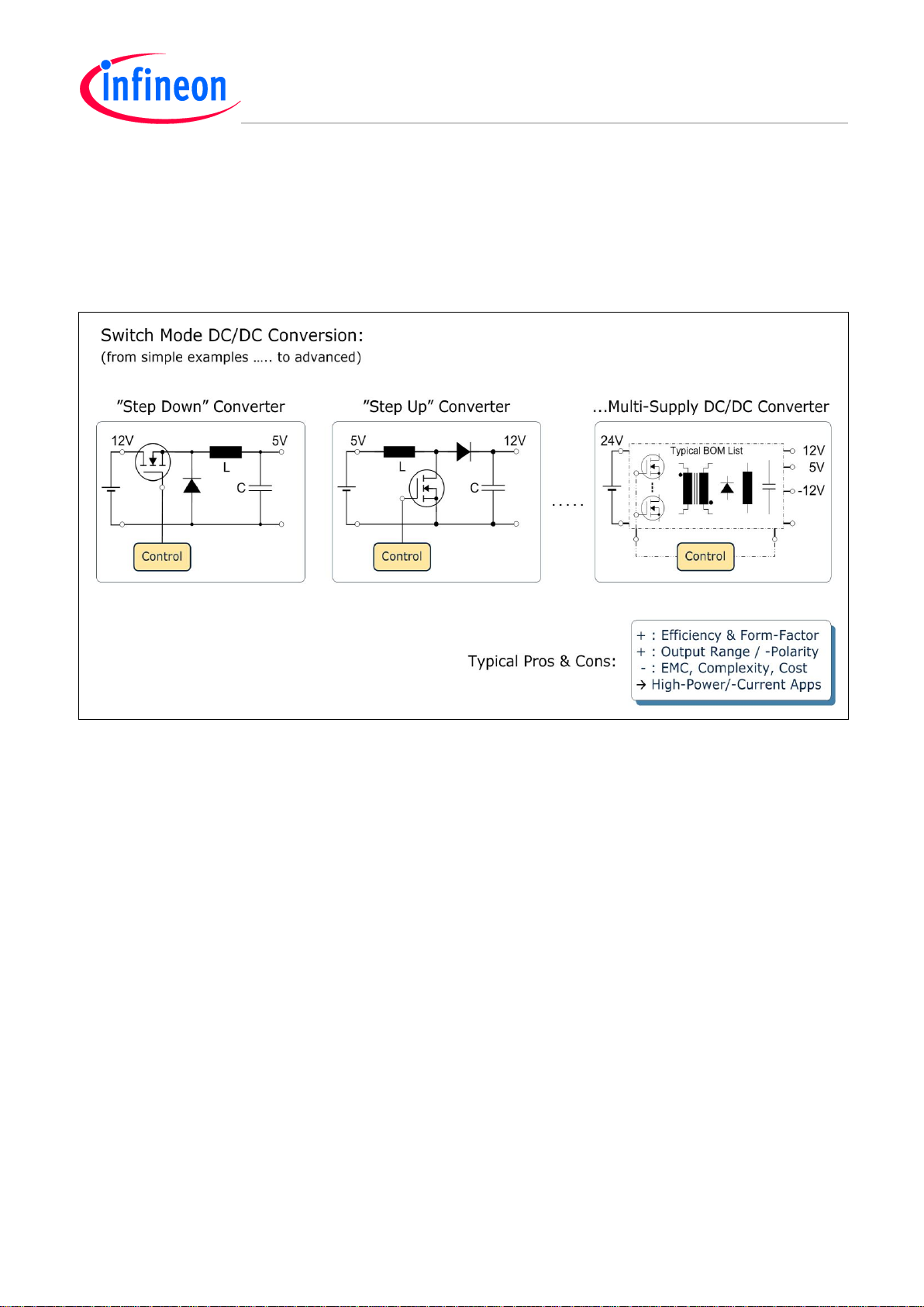
2.3.2 Switch Mode Power Conversion
A Switch Mode DC/DC Converter output/input voltage ratio can be any value, including a negative
value. That property is not covered by any Linear Voltage Converter, so most power conversion usecases can be solved by Switch Mode, especially in the area of high power, where efficiency and formfactor are vital.
Figure 2 Switch Mode DC/DC Conversion
Switch mode conversion is always an “active” conversion, in the sense there has to be active, working
semiconductors in the input-to-output transfer path. The presence of at least one winded component,
such as an inductor, is also essential.
Application Guide 9 V1.0, 2015-01
Page 10
Introduction to Digital Power Conversion
XMC4000/1000 Family
Comparison of Power Conversion Methods
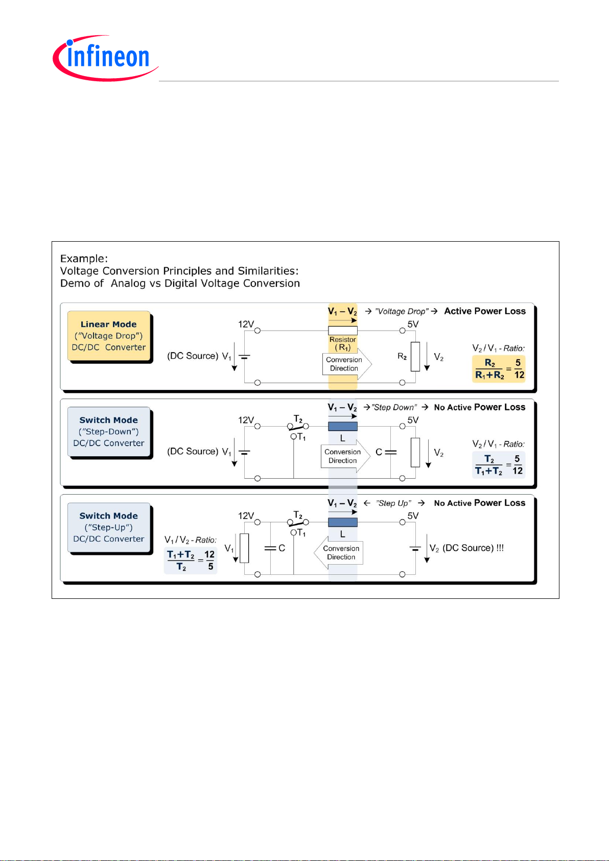
Switch Mode Power Conversion Principle – Compared to Linear Mode
In switch mode voltage conversion, portions of energy, divided by switching in time lengths (T1 or T2),
are transferred from a voltage source to an inductor (L) current as magnetic energy, cyclic in periods
(T). During the rest of each period (T), the energy is moved into a capacitor (C), for the output voltage.
This principle is true for any DC/DC converter topology.
Interesting similarities with linear conversion can be seen in the output/input voltage ratios, when
replacing ‘R’ with ‘T’. This comparison is true as long as the magnetic energy of the inductor is never
emptied before the end of each period (T); i.e. Continuous Conduction Mode (CCM) is assumed.
Figure 3 Power Conversion Principles and Similarities - Demo Model
Power Loss Comparison
The voltage drop (V
) in linear mode is maintained by a resistor (R) and constant current, causing
1 – V2
active power loss.
The voltage (V
) in switch mode is reactive by self-inductance (L) during rising or falling current in
1 – V2
the switch time intervals (T1 or T2) respectively, resulting (ideally) in no power loss.
Application Guide 10 V1.0, 2015-01
Page 11

Introduction to Digital Power Conversion
Positive properties
Negative properties
Fast
Do not adapt to new conditions during run-time
Well known
Sensitivity of parasitic effects and ageing
Simple IPs
Limited range of topologies
Standard discreet components
Narrow input / load range with efficiency
XMC4000/1000 Family
Comparison of Power Conversion Methods
2.3.2.1 Analog Switch Mode Controllers
Traditional Analog Controllers have a significant BOM (Bill of Materials) list of OpAmps, comparators,
filters, and so on. They cover just a limited range of topologies and do not adapt autonomously to
condition changes in run-time. Form factor can be poor and reusability is limited, but they are fast and
well known.
Table 2 Properties of Analog Controllers
2.3.2.2 Digital Switch Mode Controllers
Digital controllers are flexible, with a wide load / input range, and sophisticated reactions to condition
changes during run-time through multi-control loops. They are reconfigurable by software and can
connect to a network / HMI. A smart system can predict ageing or process variations, enabling
scalability and portability of IPs.
Digital Controllers – Positive properties
Cost is higher and complexity is higher too, but there are many positive properties:
Highest efficiency over wide load and input range
Sophisticated start-up algorithms
Overload condition reactions
Auto-switch between power modes (CCMCRMDCMBurst)
Programmable / configurable by software
Multiple control loops are possible
Correct real-time performance
Prediction of system behavior
Reduction of parasitic effects
Scalable for wider ranges
IPs are easily portable: lowhigh end
Fast time to market
Sophisticated reactions to events
Communication and HMI feature
Application Guide 11 V1.0, 2015-01
Page 12

Introduction to Digital Power Conversion
XMC4000/1000 Family
Comparison of Power Conversion Methods
2.3.2.3 ASIC controller versus MCU / DSP / DSC controllers
Here we outline some of the guiding properties to be considered, for the type of controller to choose
when selecting for High-end versus Low-end.
ASIC
ASIC controllers offer gate drivers and fixed optimized solutions at the lowest possible cost. They are
easy to use and they fit Low-end switch mode converters very well.
However, on the downside, they only handle known changes in load and input conditions during runtime, and reusability is limited because they are a customized solution.
Positive properties:
Custom design for known conditions
Fixed and optimized settings
Lowest possible cost
Easy to use
Embedded gate drivers
Form factor
MCU / DSP / DSC
An MCU, DSP or DSC controller brings a platform approach, a smart system with high computation
capability, and embedded power conversion orientated peripherals.
Condition changes are handled in run-time, ensuring the highest efficiency and correct real-time
performance. These features mean that the MCU, DSP or DSC solution is particularly suited to Highend power converters.
Positive properties:
Platform approach (Reuse, Extend)
When highest efficiency is required
Mixed power mode capability
Variable load / inputs
Programmable dwith software IP
Flexible communication
Application Guide 12 V1.0, 2015-01
Page 13
Introduction to Digital Power Conversion
XMC4000/1000 Family
Comparison of Power Conversion Methods
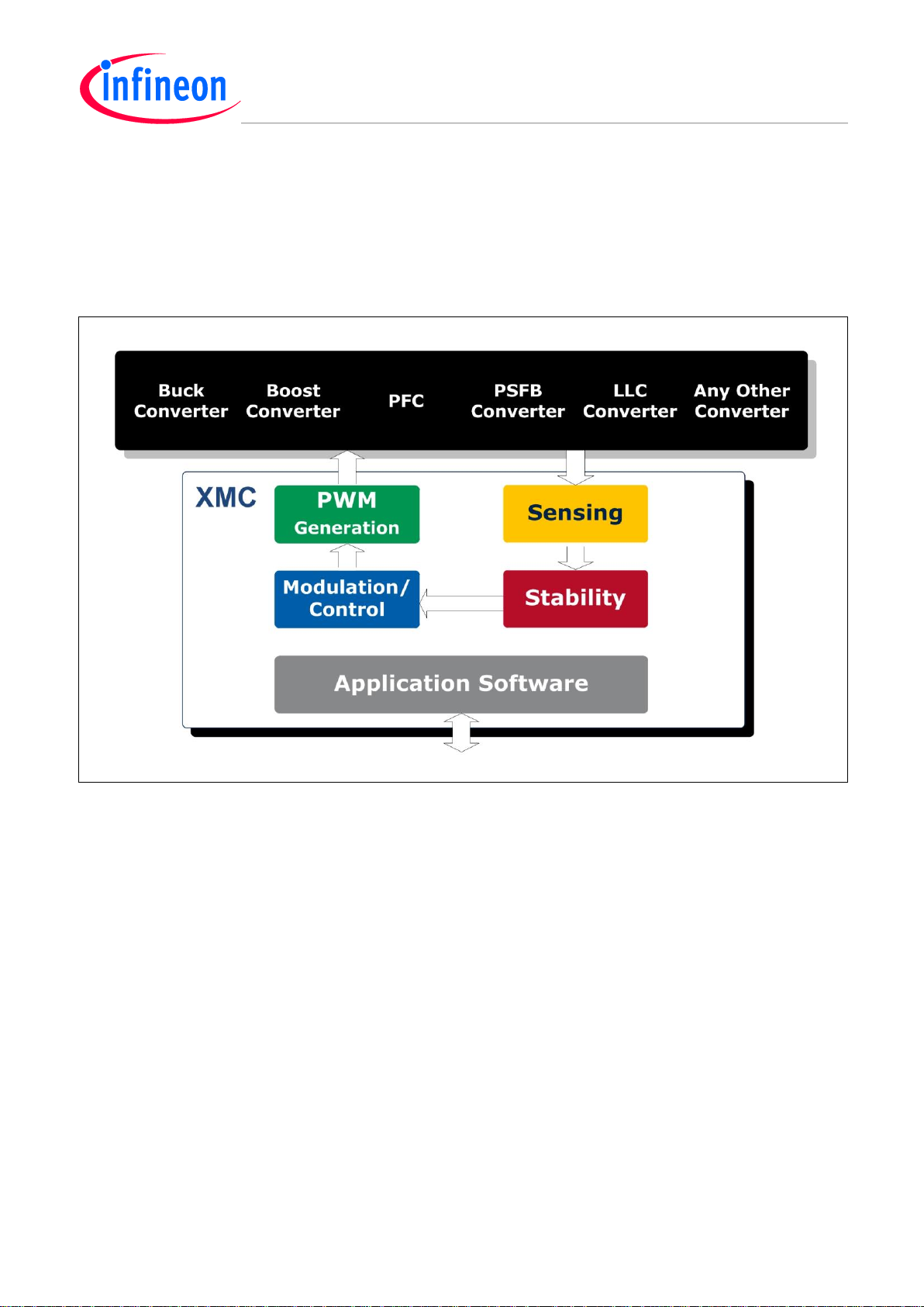
2.4 Infineon XMC-families for Switch Mode Power Control
The Infineon XMC power conversion oriented devices offer flexible 3-level control architectures, for
sense-compute-modulate-and-drive of any power converter topology.
Advanced analog and digital peripherals interact on events in real-time via a hardware matrix,
supported by DMA, Software, DSP (Digital Signal Processing) or over a network.
Figure 4 The Power Conversion Oriented XMC Devices 3-Level Architecture Control Loop
The XMC series for power control meets the performance challenges and demands of today’s
embedded control applications. The high performance, real-time capability is achieved with an ARMCortex architecture, with or without DSP, and a Floating Point Unit (FPU).
Application Guide 13 V1.0, 2015-01
Page 14

Introduction to Digital Power Conversion
XMC4000/1000 Family
Comparison of Power Conversion Methods
2.4.1 Power Conversion Oriented Peripheral Features
Here we highlight features of the XMC-family embedded peripherals that are essential for the
significant tasks required in power conversion control loops.
2.4.1.1 Sensing
Analog values are monitored, or detected upon crossing level limits, via Versatile Analog-to-Digital
Converter (VADC) channels (featuring fast compare mode), or by Analog Comparator (ACMP/CSG).
These units are interconnected with events via hardware action providers, or softwre routines via
interrupts.
The functionality of the ADCs includes:
Automatic scheduling of complex conversion sequences with priority for time-critical conversions
Synchronous sampling of up to 4 signals / Independent result registers, selectable for 8/10/12 bits
Sampling rates up to 2MHz / Flexible data rate reduction / FIR/IIR filter with selectable coefficients
Adjustable conversion speed and sampling timing
4 independent converters with up to 8 inputs w/ channel wise selectable reference voltage source
2.4.1.2 Stability and Software
An important property of conversion control loops is the frequency response of the duty-cycle-tooutput-voltage transfer function. Stabilization is provided via softwre actions in the open loop gain
paths, using DSP operations on discrete time variables, maintained by sampling at rates triggered by
a CCU (Capture and Compare Unit).
2.4.1.3 Modulation
The steady state duty-cycle-to-output-voltage transfer function is controlled by sense-modulate-drive
algorithms in hardware, with some optional add -on attributes, including (but not limited to):
Fixed-Frequency (FF)
Fixed-On-Time (FOT)
Fixed-Off-Time (FOFFT)
Conduction Mode Switching
Comparator & Slope Generation (CSG)
Blanking
Clamping
Filtering
XMC modulation modes
Voltage Mode Control (VC)
Average Current Mode Control (ACC)
Peak Current Mode Control (PCC)
Valley Current Mode Control (VCC)
Zero Crossing Detection Mode (ZCD)
The XMC peripherals handle modulation dynamically, with mode-switch on changed conditions in runtime (on load variation for example). A set of resources can be exchanged “on-the-fly” by a Mode-Bit.
Application Guide 14 V1.0, 2015-01
Page 15

Introduction to Digital Power Conversion
XMC4000/1000 Family
Comparison of Power Conversion Methods
2.4.1.4 PWM Generation
The XMC CAPCOM Units (CCU4 or CCU8) timer slices can be regarded as “timer-cells” that can
cooperate and fit together like “puzzle pieces” to form matrices of sophisticated and compound timing
functions. These can interact for certain function request events and event profile conditions.
Theoretically, any on-chip module can be considered to act on a slice via one of (up to 3) inputs. A
flexible library of modular timing control applications (PWM “Apps”) can be created and then be
reused across projects.
The XMC single and multi-channel PWM drive capabilities include:
Global Synchronization
− to ensure a fully synchronized start with any combination of CAPCOM units
PWM
− by Symmetric / Asymmetric Modulation (Edge-Aligned or Center-Aligned)
− with Active / Passive Output Level Control / Trap Handling Protocol in hardware
− with Dithering (4 bits)
− by Status Events (by Compare or Period-Control)
− by external Set/Clear (by various conditional Start/Stop functions, which can be combined with
Status Events)
− by Matrix Interactions (on specific function request events and event profile conditions)
Examples
Peak, Valley or Hysteretic On-Off PWM
Fixed-On-TIme (FOT) PWM
Fixed-Off-TIme (FOFFT) PWM
Phase-Shift / Fixed Phase-Shift (Interleave) PWM
Half Bridge (HB) control with optional Synchronous-Rectification (SR)
Full Bridge (FB) control (w/ SR)
HB / FB Drive of LLC Resonance Converters
HRPWM Attributes
High Resolution Control (HRC) Insertion – down to 150 ps accuracy:
- HRC can handle switch frequencies up to 5 MHz with 10 bit resolution PWM
- Highly Accurate Low-Load Scenario Control
- Converter Efficiency Improvement: Each HRC can operate with two set of resources
Dead Time Insertion, with “On-the-Fly” optimization during run-time.
Application Guide 15 V1.0, 2015-01
Page 16

Introduction to Digital Power Conversion
XMC4000/1000 Family
Converter Topologies
3 Converter Topologies
The fundamental power converter topologies that we focus on in this document are:
Buck (“Step-Down”) (Section 3.1)
− Conventional
− Interleaved
− Synchronous
− Inverted
Boost (“Step-Up”) (Section 3.2)
− Conventional
− Interleaved
− Synchronous
− Inverted (Buck-Boost)
PFC (”Power-Factor-Correction” (Section 3.3)
− Conventional Boost PFC
− Interleaved Boost PFC
− Bridgeless Boost PFC
− Totem-Pole Bridgeless PFC
PSFB (“Phase-Shift-Full-Bridge”) (Section 3.4)
− (Principle Scheme)
LLC (”L-L-C-resonant”) (Section 3.5)
− (Principle Scheme)
The Generic Digital Power Converter (Section 3.6)
Application Guide 16 V1.0, 2015-01
Page 17

Introduction to Digital Power Conversion
XMC4000/1000 Family
Converter Topologies
3.1 Buck
A Buck converter can only generate lower output average voltage (V
) than the input voltage (VIN),
OUT
and is therefore also referred to as a “Step-Down” converter.
The DC/DC conversion is non-isolating, in the sense that there is a common ground between input
and output. Some improved versions exist:
Figure 5 Buck
Interleaved Buck Converter
When reduced ripple and smaller components are required, especially in high-voltage applications,
then a realistic approach is to interleave the output currents from a multiphase Buck converter stage.
For example a 2-phase Buck converter controlled by fixed 180o phase-shifted PWM from an XMC
CCU4/8
Synchronous Buck Converter
When reduced power conversion loss is required, the rectifying diode D may be replaced by an active
switch that can offer a lower voltage drop. In such a solution the rectification will be synchronously
invoked by a signal that is complementary to the control signal, from a CC8 timer or CC4 timer pair.
Inverted Buck Converter
When a simplified current measurement is required, then an Inverted Buck controller is an alternative,
assuming common ground between input and output voltage is not necessary. By sensing the voltage
over a resistor (R) to ground, the inductor current (IL) can be monitored by a VADC or ACMP.
Application Guide 17 V1.0, 2015-01
Page 18

Introduction to Digital Power Conversion
XMC4000/1000 Family
Converter Topologies
3.2 Boost
A Boost converter is non-isolating and can only generate a higher output average voltage than the
input supply voltage. It is therefore called a “Step-Up” converter.
There is one exception to note however. The Inverted Buck-Boost converter theoretically generates
an output voltage from 0 to minus infinity.
Figure 6 Boost
Interleaved Boost Converter
Similar to the Buck converter, i.e. the ripple will be reduced and smaller components can be used, by
having interleaved output currents from a multiphase Boost converter stage – here by a 2-phase
Boost converter that is controlled by fixed 180o phase-shifted PWM from an XMC CCU4/-8.
Synchronous Boost Converter
A synchronous Boost works similar to a synchronous Buck – however, this variant of improvement is
not often used, since reduced power conversion loss by replacing the rectifying diode D by an active
switch is not very significant in the high voltage range – where this topology more frequently appears.
Application Guide 18 V1.0, 2015-01
Page 19
Introduction to Digital Power Conversion
XMC4000/1000 Family
Converter Topologies
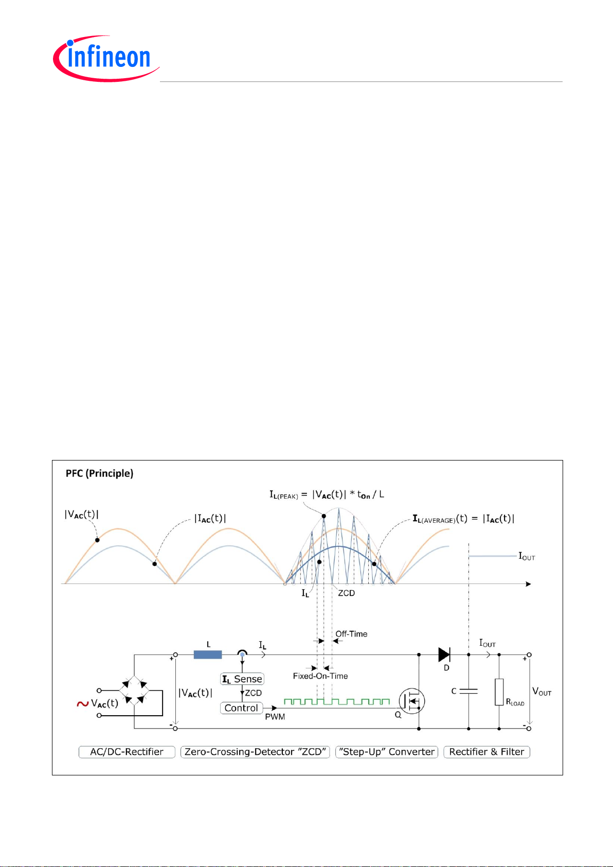
3.3 PFC
Abstract
The Power Factor (PF) is defined as the transfer ratio of real power [Watt] to apparent power [VA]:
PF = Real Power / Apparent Power [Watt / VA]
The Power-Factor-Correction (PFC) purpose is (according to the environmental context) to achieve:
Real Power = Apparent Power
i.e.:
PF = 1
PFC Rectifier
A PFC rectifier accomplishes “PF = 1” by phase correct rectification of the mains AC voltage – so that
the current conduction angle becomes fully 180o in both half periods – phase correct to the mains AC
voltage – i.e. without any parasitic or reactive signal components reflected back into the mains lines:
See Figure 7.
In principle, the mains is rectified into a sinusoidal half-wave rippling DC voltage. In turn it is converted
to a ripple-free DC output voltage by a Boost PFC – e.g. by Fixed-On-Time inductor current (IL) mode
control. (Each Off-Time interval lasts till the current (IL) falls back to Zero-Crossing-Detection, ZCD.)
Since all tOn pulses are fixed, the I
L(PEAK)
and I
L(AVERAGE)
envelopes will follow the |VAC(t)| in proportion.
Figure 7 Boost Power-Factor-Correction (PFC) – E.g. in Fixed On-Time Current Mode Control
Application Guide 19 V1.0, 2015-01
Page 20
Introduction to Digital Power Conversion
XMC4000/1000 Family
Converter Topologies
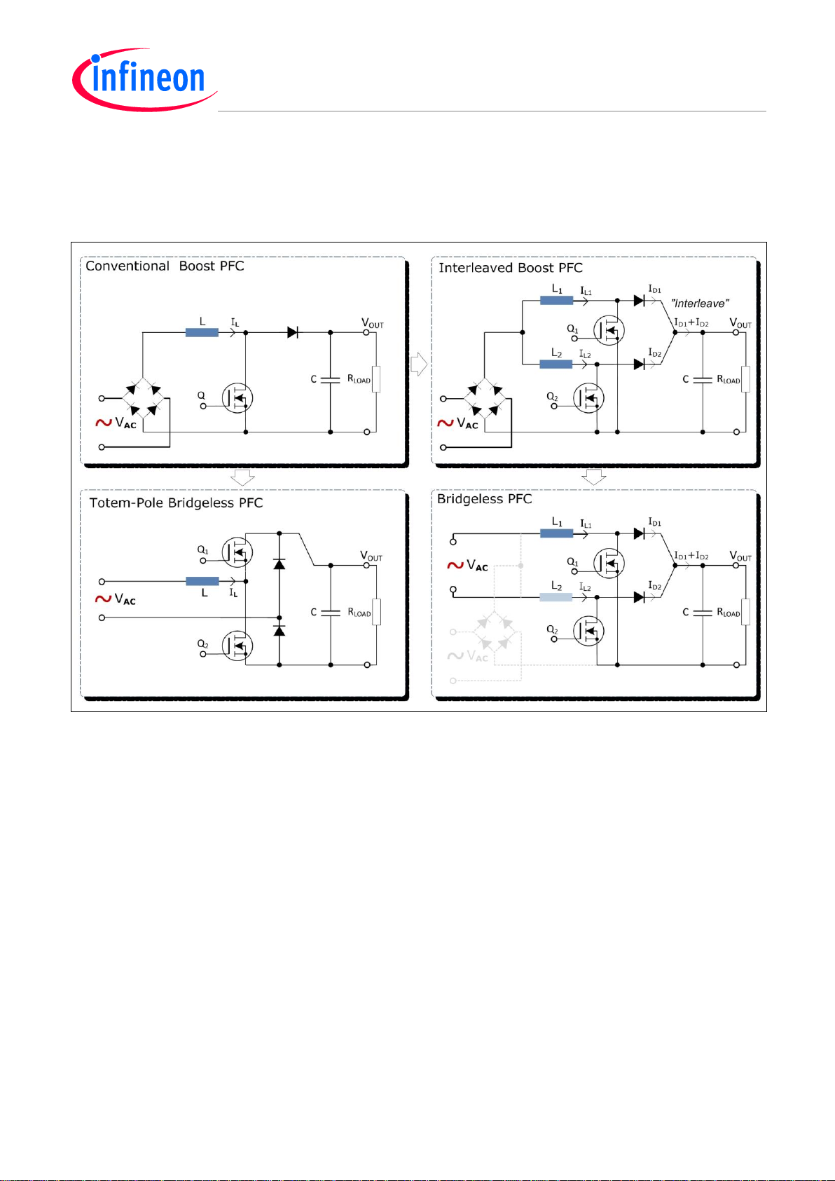
PFC Variants
There are different types of PFC circuits, which mix a balance of complexity versus performance.
Here we show just some of the basic topologies. These can be mixed into more sophisticated, multiphased, interleaved, full-bridgeless PFCs by Synchronous rectification.
Figure 8 PFC Types such as – Conventional – Bridge Interleave – Bridgeless – Totem pole
PFC Performance
High Power Factor (PF) and low Total Harmonic Distortion (THD) are directly related, so the basic
circuits can be listed in performance order, as follows:
Conventional Boost PFC
− Low cost BOM solution.
Interleaved Boost PFC (High Power)
− Even though there still is a diode bridge, the continuous interleaved current offers the advantage
of using smaller components.
Bridgeless/Totem-Pole Bridgeless PFC (High Power)
− The diode bridge is replaced by a MOSFET semi-bridge / half-bridge Totem-Pole rectifier.
Bridgeless Interleaved PFC (High power)
− (Not shown) Enables use of successive expansion of multi-phase bridgeless interleaved boost
PFC.
Application Guide 20 V1.0, 2015-01
Page 21

Introduction to Digital Power Conversion
XMC4000/1000 Family
Converter Topologies
3.4 Phase-Shift Full-Bridge (PSFB)
The PSFB is a Phase-Shift-Full-Bridge DC/DC converter. Power is transferred in a Phase-Shift (PS)
via a Full-Bridge (FB), a transformer, a rectifier and filter. The PSFB is an isolating converter.
Figure 9 PSFB Principle
PSFB power conversion stages
Stage one
− Split the DC rail input voltage (V
) into two Phase-Shifted pulse streams (PhA , PhB) according
IN
to the Full-Bridge control signals.
Stage two
− A transformer, which is fed onto its primary coil (n
) with the phase difference voltage (PhA ,
p
PhB). This difference voltage will be transformed with a ratio (ns : np) to two secondary coils (ns ,
ns).
Stage three
− A “step-down” converter configuration with two diodes (D
positive levels of the two secondary voltages respectively into a PWM pulse stream. These
PWM pulses have a duty cycle that corresponds to the phase shift |Ph
, DB) that rectify and interleave the
A
o
Ao – PhB
|, and will be
filtered via the inductor (L) into the output capacitor (C), and result as an output voltage (V
− The PSFB total voltage conversion ratio (V
ratio (ns : np) times the phase-shift |Ph
Ao – PhB
/ VIN) is proportional to the transformer winding-
OUT
o
|:
V
/ VIN = (ns : np) * |Ph
OUT
Ao – PhB
o
| / 180
o
OUT
).
Application Guide 21 V1.0, 2015-01
Page 22

Introduction to Digital Power Conversion
XMC4000/1000 Family
Converter Topologies
3.5 LLC (Inductor-Inductor-Capacitor)
The LLC converter is a series resonant converter. Power is transferred in a sinusoidal manner, so the
switching devices are softly commutated by ZVS (Zero-Voltage-Switching) and without capacitive
loss. A transformer takes part in the process, making the LLC an isolating converter.
Figure 10 LLC Principle – Using Half-Bridge Control
Performance
A resonant converter enables high voltage and faster switching, which allows for smaller components
thanks to the reduced switching losses.
An LLC converter, with two inductors (Lr ,Lm) and a capacitor (Cr), is superior to all other types of
resonant converters, especially with respect to a wide load range.
Properties
The LLC inductor Lm shunts the transformer primary coil when the impedance becomes infinite:
If there is no diode current, the resonant tank will become “(L
If there is diode current, the tank is “L
“. Therefore open load can be handled. The power
rCr
r +Lm)Cr
“
transfer is tuned by frequency or PWM.
Application Guide 22 V1.0, 2015-01
Page 23
Introduction to Digital Power Conversion
XMC4000/1000 Family
Converter Topologies
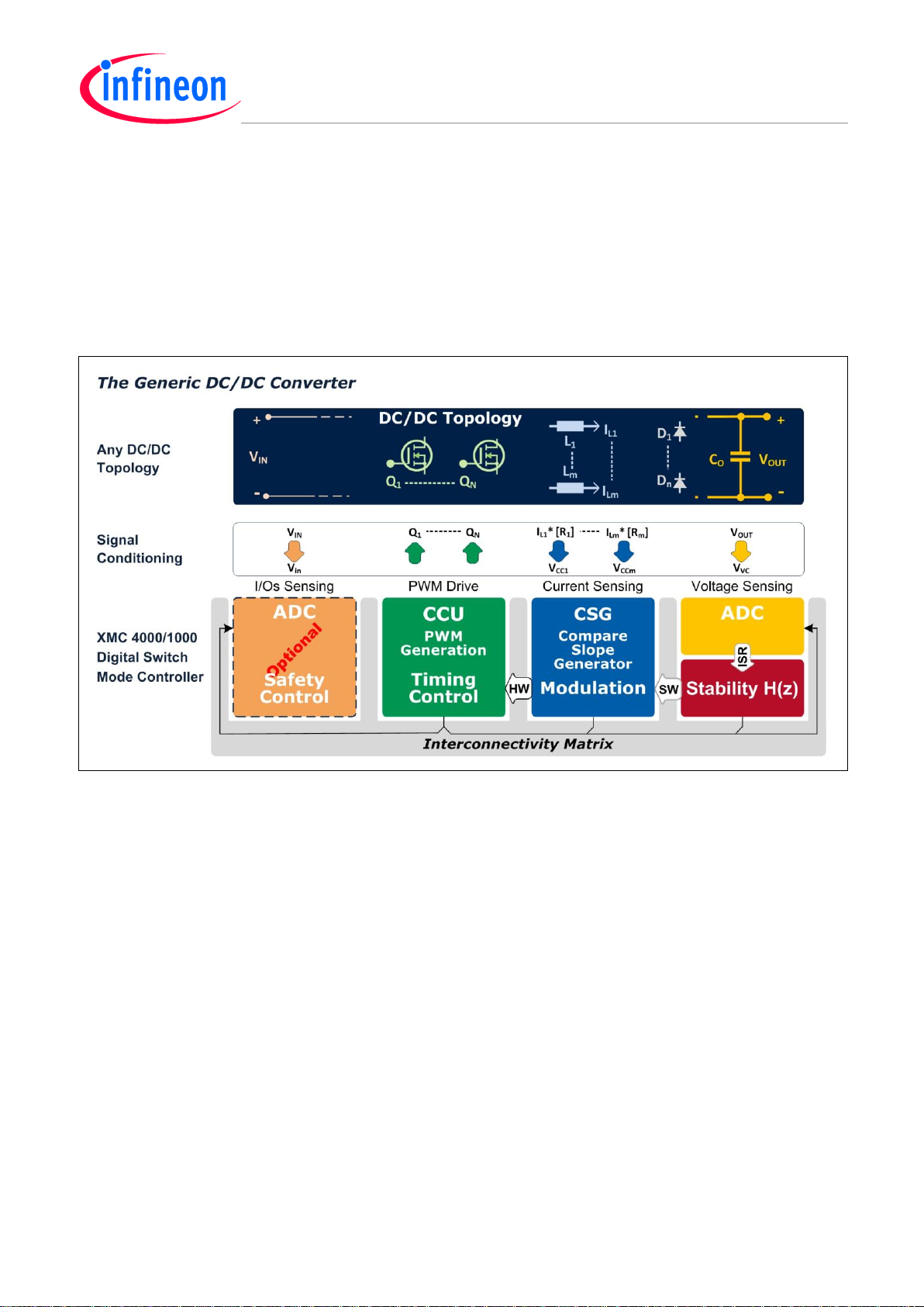
3.6 Generic Digital Power Converter
There is a mutual property of all DC/DC power converters: Energy from an input power source is
periodically stored as magnetic energy in the air-gap of inductors (L), and converted into certain
output power voltage-current pairs via some rectifier-and-capacitor (C) filter configuration.
Because of this property, the essential components and control loops for Switch Mode DC/DC power
converters can be described by a “Generic DC/DC Converter” that is representative for all topologies
of this type.
Figure 11 The Generic Switch Mode DC/DC Converter.
Key Attributes
Generic hardware protocol
Flexible Drive and Sense Interfaces for Feed-Back Loop Control of Voltage and Current Transfers
Modular Loop Control by Event Interconnection Paths between XMC Embedded Unit Functions
Global Start and Synchronization Features
Application Guide 23 V1.0, 2015-01
Page 24

Introduction to Digital Power Conversion
XMC4000/1000 Family
PWM Generation
4 PWM Generation
4.1 Single Channel
The PWM duty cycle range is 0 – 100% for all available combinations of alignments, count and
in/output modes.
Status bit ST can be set to 1 or 0 by timer compare or period events, or by external events (even if
stopped timer).
An output can be set active high or low (and with Dead-Time in CC8).
Figure 12 PWM – Single Channel
4.2 Single Channel with Complementary Outputs
A single channel (Ch1/-2) of a CC8y timer slice can output a complementary PWM signal pair in any
alignment mode. It may include Dead-Time Insertion of individual rise-/fall times, as well as accurate
active level settings for 1 or 2 half-bridges. The Trap input coordinates shut-down in correct real-time.
Figure 13 PWM – Single Channel Half-Bridge Drive
Application Guide 24 V1.0, 2015-01
Page 25
Introduction to Digital Power Conversion
XMC4000/1000 Family
PWM Generation
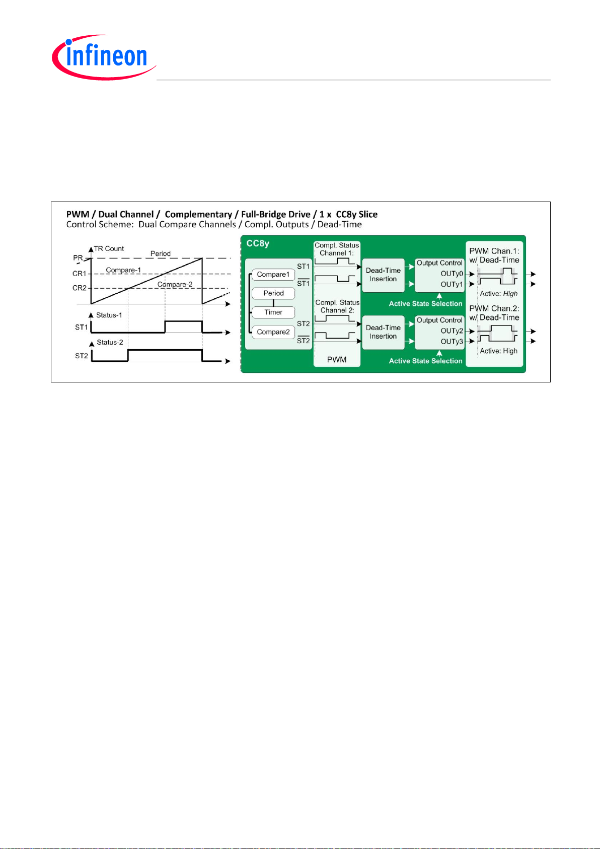
4.3 Dual Channel with Complementary Outputs with Dead-Time, using CCU8
By using both channels (Ch1 and Ch2) in a CC8y timer slice, it is possible to output a dual pair of
complementary PWM signals to target 1 or 2 full-bridges.
Dead-Time insertion of individual rise-/fall times can be provided independently, as well as accurate
output active level settings and trap care.
Figure 14 PWM – Dual Channel Full-Bridge Drive
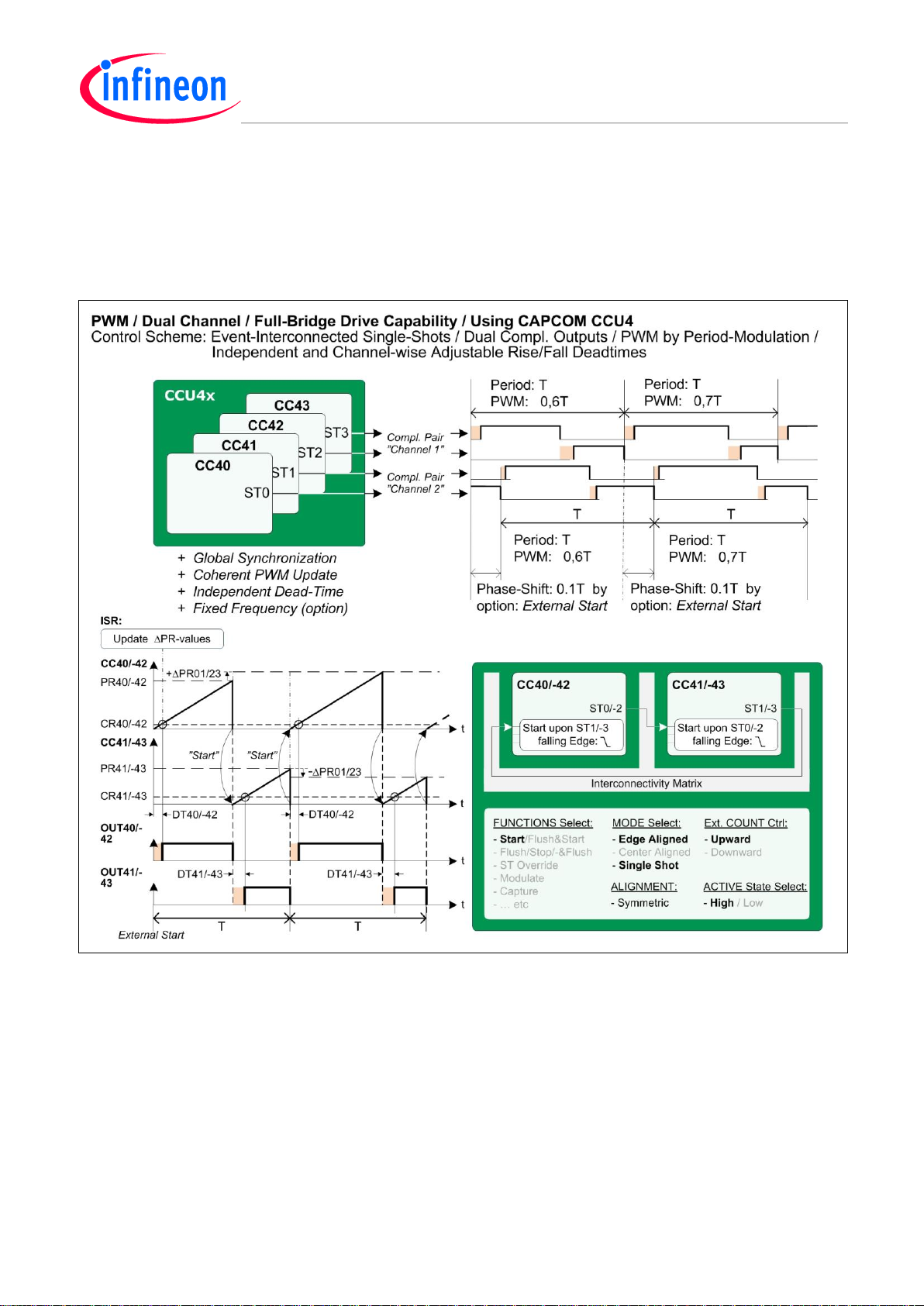
4.4 Dual Channel with Complementary Outputs with Dead-Time, using CCU4
A ‘sea’ of individual ‘timer-cells’
The timer slices of all CCUs can be regarded as a ‘sea’ of individual ‘timer-cells’ that are
interconnectable to act upon each other’s event requests, and accomplish dedicated and compound
timing functions.
Event sources and function commands are easily mapped by registers: CC4(8)yINS and
CC4(8)yCMC.
A typical example is a CCU4 Full-Bridge drive with complementary outputs and individual Deadtimes
(see Figure 15).
PWM with Complementary Outputs by Using CCU4 Single-Shot Timers
A complementary PWM output pair can be built from two timer slices (e.g. CC40 and CC41) in singleshot mode. The timers run, one at a time so that when one timer stops after its single-shot, it starts
the other timer with an event request Input Function ‘Start’. This can be mapped via interconnect
settings.
PWM with Dual Complementary Outputs by Using Synchronized Single-Shot Timer Pairs
When adding the other two timer slices of a CCU4 (e.g. CC42 and CC43), Full-Bridge control is
possible. Dead-Time insertion can be added and the ‘channel 1’ and ‘channel 2’ (CC40/41 and
CC42/43) can be synchronized with a Global Start.
PWM with Complementary Outputs Including Dead-Time Insertions
By using a preset compare register to shorten the output width of each single-shot, it is possible to get
individual deadtimes for different switch delays, and enable a Full-Bridge drive capability with a
CCU4.
Note: The pulse width modulating role is performed by period registers – not by compare registers.
Application Guide 25 V1.0, 2015-01
Page 26
Introduction to Digital Power Conversion
XMC4000/1000 Family
PWM Generation
PWM Duty-Cycle Control by Period Register
PWM modulation (with fixed cycle period target option) is achieved by adding a ∆PR-value and
respectively substracting the same ∆PR-value to the period registers of the PWM channel single-shot
timer pair. Updates are via period shadow registers, by compare-ISR, and are set on shadow
transfers.
Figure 15 PWM – Dual Channel / Complementary Outputs w/ Individual Deadtime
PWM Phase-Shift Control by External Start of Single-Shot Timer Pairs
The coherent update mechanism via shadow transfers can be used to control a certain Phase-Shift
magnitude between the two slice-pairs, in this instance CC40/41 and CC42/43 respectively.
A good example, using just a CCU4 in this concept, is Fixed Phase-Shift Control with Zero-Voltage
Switching (ZVS) (See Figure 27).
Application Guide 26 V1.0, 2015-01
Page 27
Introduction to Digital Power Conversion
XMC4000/1000 Family
PWM Generation
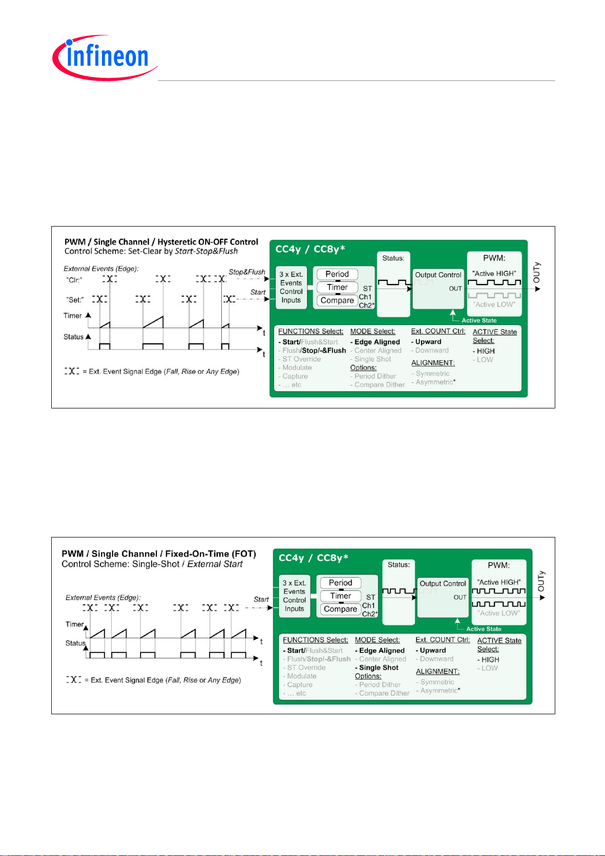
4.5 ON/OFF Control
Since all the individual ‘timer-cells’ of a CCU can be mapped to act upon virtually any external event
and function request, then theoretically any on-chip module can be considered to control a PWM. For
example, an ADC or comparators can join in the PWM control loops in this way, acting on analog
events. With such configurations, variable frequency and/or PWM pattern control is easily
accomplished.
Figure 16 PWM On/Off Control by External Events
4.6 Fixed ON-Time (FOT)
Fixed-On-Time (FOT) PWM has two essential properties:
1. The FOT Pulse Width is generated by a fixed active output state of a timer, by single-shot mode
for example.
2. The FOT Pulse Rate is controlled by external events; i.e. the timer does not decide pulse density.
Duty-cycle should be monitored for example, to enable feed-back control in the start-up phase.
Figure 17 PWM with Fixed-On-Time (FOT)
Use Case
FOT can be used in a PFC with inductor current ZCD in the control loop (See Figure 18).
Application Guide 27 V1.0, 2015-01
Page 28

Introduction to Digital Power Conversion
XMC4000/1000 Family
PWM Generation
4.7 Fixed ON-Time with Frequency Limit Control
In power switch control with FOT PWM, it is mandatory to have pulse rate limiting add-ons in the loop,
ensuring a minimum of off-time to be fed back by the conversion process in each FOT start request.
Another extreme is maximum off-time.
Both extremes will require ‘f
timer’ add-ons in the loop.
max–min
Figure 18 FOT Control with Frequency Limits Supervision
The FOT Timer (Slice1)
Assume that this single-shot FOT timer works in a CRM or DCM mode PFC controller. In each switch
cycle the timer waits for a start request in the control loop, after a certain off-time. Then it will switch
on the inductor current for a fixed time, to rise from zero again, on any of the following conditions:
ZCD AND f
An early ZCD event AND before expired f
f
Application Guide 28 V1.0, 2015-01
-period expires AND there was no ZCD event in the meantime // DCM, FOT at ‘Time-Out’
min
-period is due // CRM, FOT density OK
max
-period // DCM, FOT pulse delayed
max
Page 29

Introduction to Digital Power Conversion
XMC4000/1000 Family
PWM Generation
The ZCD Event Window (Slice3)
There is a memory function required to keep track of a ZCD event that might happen before a FOT
pulse is allowed to start, due to the f
Instead of using an ERU, a timer slice (Slice3) can be used to define an ‘allow’ window by ‘Start-uponZCD and Stop&Flush upon falling FOT’.
-period restriction.
max
Figure 19 Interconnectivity between CCU4 slices for PWM FOT Control with Frequency Limits
Application Guide 29 V1.0, 2015-01
Page 30

Introduction to Digital Power Conversion
XMC4000/1000 Family
PWM Generation
Monitoring the FOT pulse rate
The FOT pulse rate is monitored by the free running f
each FOT timer start.
If the next ZCD event occurs before the f
because of f
-period. If no ZCD occurs, then the FOT-start has to wait for the timeout.
max
The FOT timer will start on the falling edge of the f
-period compare event, then the next FOT start must wait
max
max–min
There can be any of three different event flow scenarios behind a FOT pulse start, depending on
whether the ZCD-event occurs after or before the ZCD, or if there is no ZCD at all, in relation to the
f
-period compare event (here named CMP-event).
max
All event flow scenarios will terminate by an end-of-FOT event, alias EOF-event.
Notes:
1. For readability, all redundant actions in the event flows described here have been removed.
2. All event flow scenarios will begin and end with the status bit of all timers = 0; i.e. ST0=0, ST1=0, ST2=0,
ST3=0.
3. = “consequently the successive event will follow”.
4. // = “a parallel (synchronous) event flow, connected to the root event”.
5. STn=STm means “Status-bit Override; i.e. status bit STn is copied with status bit STm”.
6. # = “inverted value of”.
timer (Slice2). This timer is flushed on
max–min
timer status.
CRM Mode: Event Flow ‘after’
i.e. ZCD-event > CMP-event
1. CMP-event: ST2=1
2. ZCD-event: ST1=ST2 ( FOT) flush-Slice2 ST2=0 start-Slice1
3. EOF-event: ST1=0
DCM Mode: Event Flow ‘before’
i.e. ZCD-event < CMP-event
1. ZCD-event: Start-Slice0 // Start-Slice3 ST3=1 (delayed 1 clk by compare)
2. CMP-event: ST2=1 capture-Slice0 ST0=1 ST2=#ST3 start-Slice1 ST1=1 (
FOT) (flush-Slice2 + stop&flush-Slice0)
3. EOF-event: ST1=0 stop&flush-Slice3 ST3=0
Event Flow “No ZCD”
No ZCD at all until due f
-period = Timeout at Slice2 Period-Match
min
1. CMP-event: ST2=1
2. Timeout: ST2=0 Start-Slice1 ST1=1 ( FOT) flush-Slice2
3. EOF-event: ST1=0
The Auxiliary Timer (Slice0). Monitoring the DCM Window
This timer is essential for the status bit-override “ST2=#ST3” operation specifically, since there is no
direct “ST2=1 ST2=#ST3” event interconnectivity path; i.e. a slice cannot event request itself.
Optionally, Slice0 will work as a DCM window monitor.
Application Guide 30 V1.0, 2015-01
Page 31

Introduction to Digital Power Conversion
XMC4000/1000 Family
PWM Generation
4.8 Fixed Off-Time (FOFFT)
In Fixed Off-Time switch mode, each PWM On-Time pulse is variable and terminated when the
inductor current slope hits the peak-current detection level.
On each of these events the current slope will fall, with a fixed Off-time, before next pulse, controlled
by a timer. This could be the PWM timer itself for example.
FOFFT by Load Timer Function – How it works
The load-timer mode is an alternative way of creating a fixed Off-time interval.
The compare register value is copied into the timer register by a load-timer request on a peak
detection event.
From this event, until period match, the rest of the timer cycle is a fixed time (period value minus
compare value).
FOFFT mode with On-Time Limitation
The advantage of using the load-timer mode solution in Fixed Off-Time PWM generation, is that an
optional On-Time limitation is left “for free”, to be an add-on feature in the extension; i.e. a compare
event will come and terminate the On-Time even if a load-timer request does not appear.
FOFFT with Blanking
To avoid inaccurate peak current detections due to noise from the power switches, blanking time
zones should be invoked, during which all detection events by the analog comparator should be
rejected.
Blanking should be synchronized to the start event of each PWM cycle (See section 6.4).
Figure 20 PWM with Fixed-Off-Time (FOFFT)
Application Guide 31 V1.0, 2015-01
Page 32

Introduction to Digital Power Conversion
XMC4000/1000 Family
PWM Generation
4.9 Phase Shift Control
There are two types:
Fixed Phase Shift (180
Variable Phase Shift
o
, 120o, 90o, and so on)
Fixed Phase Shift
This is used for interleave applications with multi-phase converters. The interleave function has the
benefit of overlapping discontinuities in the current path, reducing ripple and therefore allowing for
higher frequency and smaller components. EMC quality is also improved.
Variable Phase Shift
This is used for DC/DC conversion applications, and for energy transfer adaption and isolation, by
using a transformer in the path. The changes in the phase-shift modify the power transfer from
primary to secondary.
4.10 Fixed Phase-Shift
4.10.1 Center Aligned Mode
Dual PWM channels with guaranteed 180o fixed phase-shift even during the PWM update, is provided
by a single CCU8 slice in symmetric compare mode for two PWM channel outputs: OUT01, OUT02.
Passive/Active Level:
− for OUT01 is “ACTIVE HIGH”
− for OUT02 is “ACTIVE LOW”
Figure 21 Fixed Phase-Shift – Using a CC8-Slice in Center Aligned Symmetric Compare Mode
Application Guide 32 V1.0, 2015-01
Page 33

Introduction to Digital Power Conversion
XMC4000/1000 Family
PWM Generation
4.10.2 Edge Aligned Mode
Dual PWM channels with fixed phase-shift can be provided by two CCU4 slices in edge-aligned
compare mode, representing each PWM channel by the associated output of each status bit.
There should be a Global Start and Synchronization sequence, before the system is prepared for runtime.
Figure 22 PWM – Fixed Phase-Shift in Edge Aligned Mode for Interleave
Start-up sequence
During the start-up phase the duty-cycle of CC40 is set to 0 by pre-setting a high compare level,
exceeding the period register value pre-set, which implies no PWM generation during the start-up. A
similar situation prevents the CC41 from generating a PWM stream too early.
Fixed Phase-Shift with Different Duty-Cycles
There is no negative effect, but there can be a benefit, to using fixed phase-shift in edge aligned
mode with different duty-cycles, especially in split converters using a mutual controller. The split in
time will mean that the EMC qualities will be better.
Application Guide 33 V1.0, 2015-01
Page 34

Introduction to Digital Power Conversion
XMC4000/1000 Family
PWM Generation
4.10.3 Interleave
The Interleave approach offers reduced current ripple and a continuous current flow into the rectifier
and filter output stage of the converter. A higher frequency and smaller components can be used.
This concept is often used in high power, high voltage (e.g. PFC) and/or ZVS quasi-resonant
converters.
Figure 23 PWM – Interleave – Fixed Phase-Shift – (Modulation 50%)
Application Guide 34 V1.0, 2015-01
Page 35

Introduction to Digital Power Conversion
XMC4000/1000 Family
PWM Generation
4.11 Variable Phase-Shift
A Phase-Shift Full-Bridge (PSFB) offers the benefits of using a transformer in the DC/DC conversion
path, for level adaption or isolation.
The phase-shift of two PWM signals to the bridge control inputs converts the bridge DC rail voltage
proportionally to a transformable AC-voltage, with a defined ratio (See also Figure 9).
The target DC output voltage is rectified and LC-filtered after the secondary coils of the transformer.
PWM Phase-Shift by Master-Slave Timer Configuration
The PSFB phase-shift control signal-pair should be generated by one master timer that can guarantee
a fixed PWM pulse rate, and one slave timer in single-shot mode for the phase-shifted PWM pulses,
which should be controlled by the master timer as follows:
CC80-Channel1 controls the phase-shift by variable compare events that starts the slave PWM
cycle as single shots
CC80-Channel2 compare events generate the free-running master PWM
Other setups might cause issues on big phase-shifts.
Note:
1. The suggested timer configuration allows for the highest possible phase-shift dynamic (-180o to +180o).
However, in most practical power conversion use cases with PSFB, 180o dynamic range is enough.
2. It is possible to vary the Duty-Cycles of each signal in the PWM phase-shift pair to any extent (Not shown
here).
Figure 24 PWM – Variable Phase-Shift by Master-Slave Timer Configuration
Application Guide 35 V1.0, 2015-01
Page 36

Introduction to Digital Power Conversion
XMC4000/1000 Family
PWM Generation
PWM Phase-Shift Master-Slave Principle
A CC8-slice (e.g. CC80) and its two compare channels can be used as a master for the PSFB control
as follows:
Channel1
− The CC80CR1 compare events control the phase-shift of the PWM pulse stream (S) from a
slave timer (e.g. CC81), by requesting one single-shot PWM pulse upon each compare event.
Channel2
− The CC80CR2 compare events generate the fixed PWM pulse stream (M).
Figure 25 PWM – Variable Phase-Shift Master-Slave Principle in Detail
Application Guide 36 V1.0, 2015-01
Page 37

Introduction to Digital Power Conversion
XMC4000/1000 Family
PWM Generation
4.11.1 Power Conversion Control Example
The PSFB controller performs DC/DC power conversion in stages:
1. Split the DC input voltage (VIN) in to two phase-shifted pulse streams (PhA and PhB), controlled by
a PWM Phase-Shift-Master-Slave configuration with the CCU8 slice pair CC80/-81 (See also
Figure 24).
2. Invoke a transformer, which offers an isolating path for the voltage difference PhA minus PhB, on its
primary coil, over to the next stage, via two complementary secondary coils.
3. A “step-down” converter configuration is used, with synchronous rectification with the switch-pair
(Q3, Q4), as an efficient replacement for diodes by offering lower voltage drop.
− The switch-pair (Q
voltages from the transformer into a PWM pulse stream. The PWM will get a duty cycle that is
proportional to the phase shift |Ph
− The inductor (L) and the output capacitor (C
, Q4) rectifies and interleaves the positive levels of the two secondary
3
o
– Ph
A
o
|.
B
) serve as an LP-filter for the output voltage (V
O
OUT
).
Figure 26 PWM – Variable Phase-Shift Control – Example Using Synchronous Rectification
There is a fast Current Mode Control loop, sensed by a Fast Compare VADC channel, via a stage ‘R’
acting as trans-resistance, and there is a slow Voltage Mode Control loop via another VADC channel.
The MOSFETs require some kind of isolating driver stage (e.g. opto-couplers).
Application Guide 37 V1.0, 2015-01
Page 38

Introduction to Digital Power Conversion
XMC4000/1000 Family
PWM Generation
4.11.2 Zero-Voltage Switching (ZVS) Control
ZVS implies nearly lossless transitions. In combination with smooth zero crossing by resonance
components, an almost ideal switching process is achievable. This effect can be made by controlling
the free-wheeling currents and using the parasitic stray reactive elements (See also Figure 27).
Instead of using a traditional, combined control of the diagonal switches, there are individual delays
implemented to focus the ZVS spots to occur in appropriate time, and to keep the free-wheeling
current polarity unchanged.
Free-wheeling Current Control by Active Clamp
When the upper (or the lower) switches are conducting simultaneously, due to the phase shift, the
transformer and the free-wheeling inductive current path is short circuited to the upper (or lower) input
voltage rail.
The time-constant (‘L/R’) almost reaches infinity with this current on-holding active clamp.
ZVS Control
During the delay, in front of each turn-on event, the switch remains off and is clamped to a zero
voltage drop by the resonance effect.
The switch is held off while the free-wheeling current circulates via a body diode and the opposite leg
switch, still on. The inductive energy has to last for this though.
Figure 27 PWM – Phase-Shift-Full-Bridge (PSFB) with Zero-Voltage Switching (ZVS)
Application Guide 38 V1.0, 2015-01
Page 39

Introduction to Digital Power Conversion
XMC4000/1000 Family
PWM Generation
4.12 Adding High Resolution Channel (HRC) – HRPWM
There are devices in the XMC family series offering High Resolution Channel (HRC) Generation.
The High Resolution PWM (HRPWM) can be used with the CC8 slices and the CSG (Comparator and
Slope Generator). The output pins are with or without HRPWM.
Figure 28 High Resolution Channel (HRC) Add-on Principle
Properties
Each one of the High Resolution channels is capable of addressing up to 2 complementary MOSFET
switches, and Set/Clear may be mapped to different sources.
Flexible Set / Clear Switch in Runtime
Any combination of the four CC8y slices and the three CSGs units may act as the Set/Clear source
pair, with individual event profile conditions. The set/clear setup may be changed as required during
runtime.
Insertion
The enhanced PWM resolution is performed by insertion that shortens or lengthens the original pulse
width of the CCU8 slice output pulse stepwise, in lengths of 150 ps within the LSB.
Performance example: The HRPWM offers a resolution of 10-bit up to 5 MHz PWM.
Application Guide 39 V1.0, 2015-01
Page 40

Introduction to Digital Power Conversion
XMC4000/1000 Family
PWM Generation
Output
The HRPWM path offers dynamic Dead-Time Insertion and Active Output Level Selection.
4.12.1 PWM Dead-Time Compensation
The Dead-Time parameters for rise or fall-time can be independently changed, at any time, in any
mode, from one switch cycle to another. This is useful for adapting to load variations.
The XMC devices make use of this in order to maintain an optimized efficiency.
Figure 29 Dead-Time Compensation
Updating the Dead-Time
There are two methods:
1. Linked to one of the timers
2. Linked to the Dead-Time timer overflows
Source Switching (Mixed Mode)
There is switch mode-bit, by which the source setup that can be used in switching between CCM (i.e.
only timer control) and CRM (i.e. timer plus comparator), can be exchanged on demand, by request.
Application Guide 40 V1.0, 2015-01
Page 41

Introduction to Digital Power Conversion
XMC4000/1000 Family
PWM Generation
4.13 Half-Bridge LLC Control using ½ CCU4
LLC Converter Power Transfer by Pulse Frequency Modulation Control (PFM)
The power transfer through an LLC converter can be controlled by frequency and/or PWM. The
operating point should focus on the inductive property slope of the gain-vs-frequency characteristic
curve, where the current phase is delayed and the gain will be reduced by increasing the frequency.
LLC Converter using a pair of Inter-connected CCU4 Slices in Single-Shot Mode
Figure 30 Half-Bridge LLC Converter – Using CCU4
50% duty-cycle and center aligned modulation (referenced to the sinusoidal voltage zero-crossings)
can be achieved by two timer-cells in equal single-shot mode, interacting by alternately starting each
other.
PWM tuning may be added onto the invoked dead-times and be controlled by the compare registers.
Note: This configuration can also be made by a single CC8y slice timer (See Figure 32).
LLC Converter Power Transfer by PWM Fine-Tuning Control
PWM duty-cycle also impacts on the power transfer through an LLC converter, since the amount of
energy is cycle wise injected into the resonant tank. This enables output level fine-tuning.
Application Guide 41 V1.0, 2015-01
Page 42

Introduction to Digital Power Conversion
XMC4000/1000 Family
PWM Generation
4.14 Half-Bridge LLC Control - Synchronous Rectification using CCU4
A single CCU4 CAPCOM unit is capable of driving an entire LLC converter with synchronous rectifier.
Dead-time insertions are implemented in all switch commutations.
The MOSFETs in the rectifier stage offer lower voltage drop than diodes do for high currents. The
control paths to Q3,Q4 assume isolation.
Figure 31 PFM – Using Half-Bridge LLC – Synchronous Rectification
LLC Control by Matrix-Interaction Paths in the Timer Cell Pair Setup with CC40/41 and CC42/43
All four timers work in single-shot mode. The CC40/41 timer pair interacts by alternating start requests
on a period match. However the timer CC42 is acting as a slave to the timer CC40: It will start the
CC42 on a compare match. This relationship and action is the same from timer CC41 to timer CC43.
LLC Control by Frequency, Dead-Time Delays and PWM Tuning
Frequency is changed by simultaneous period register updates by hardware (via shadow transfer
requests from the software). Dead-Times are controlled individually by compare registers.
Power transfer tuning can be accomplished by add-on control of compare registers, or by shortening
the CC42/43 single-shots.
Application Guide 42 V1.0, 2015-01
Page 43

Introduction to Digital Power Conversion
XMC4000/1000 Family
PWM Generation
4.15 Full-Bridge LLC Control Using HRC – Synchronous Rectification
Here slices from different CAPCOM units (CCUs) interact on event control.
A CCU8 slice timer (CC80) creates Pulse-Frequency Modulation (PFM), optionally with PWM for Full-
Bridge control. CC80 is master of the synchronous rectifier (CC42/43).
Note: The slices CC42/43 in this example can be replaced by a CCU8 slice configuration.
Figure 32 Full-Bridge LLC Control w/ Synchronous Rectification – Using HRPWM
LLC Control by Frequency and Fine Tuning by HRPWM
The PFM and the PWM are simultaneously updated in the CC80-timer period and compare-registers.
Power transfer tuning is invoked by the High-Resolution Insertion (HRI) and Dead-Time Insertion
(DTI), between status-bits (CCST1/-2) and bridge inputs. Tuning is also possible with the CC42/43
periods.
Application Guide 43 V1.0, 2015-01
Page 44

Introduction to Digital Power Conversion
XMC4000/1000 Family
PWM Generation
4.16 Full-Bridge LLC Control – Synchronous Rectification Using HRC
The Full-Bridge LLC control by Pulse-Frequency-Modulated (PFM) and complementary PWM signalpairs, with individual Dead-Time Insertions, offer a tailor-made matrix of variables for an LLC
converter, including a phase adjustable synchronous rectification for alignment to the sinusoidal
current phase.
Figure 33 PWM – Full-Bridge LLC Control – Phase-Adjusted High-Resolution Rectification
Adjusting the Synchronous Rectification Phase Compliantly to the Sinusoidal Current Phase
The synchronously running timers (CC80 and CC81) may be phase-adjusted, on-the fly, in order to be
mapped optimally to the voltage switching phase and the current phase respectively. This will focus
the rectifier operation for the best efficiency, combined with the high-resolution insertion by the HRC.
Application Guide 44 V1.0, 2015-01
Page 45

Introduction to Digital Power Conversion
XMC4000/1000 Family
PWM Generation
Synchronous Rectification Phase-Shift by Using the Timer-Load Input Function
This alternative, to phase-shift a PWM, is useful here. The CC81 timer-load input function needs to be
mapped in the interconnection matrix to be requested on every CC80 One-Match event. The
CC81CR2 register is chosen as a timer load source, acting as a type of “mailbox” for every new
phase-shift (Ref.: CC8yTC.TLS register).
The phase-shift procedure, after the interconnectivity for the timer-load function is setup, is as follows:
Each new phase-shift value must be written into the CC81CR2 register (This can be done at any
time).
On every CC80 One-Match event (at valley point), the CC81 timer will be loaded with this value.
Synchronous Rectification Control with High Resolution PWM (HRPWM)
The CC81CR1 register is used in compare mode to generate the PWM stream that Set/Clear triggers
the HRCy channel to output synchronous rectification control of the MOSFET-stage (Q3 , Q4).
Application Guide 45 V1.0, 2015-01
Page 46

Introduction to Digital Power Conversion
XMC4000/1000 Family
Sensing
5 Sensing
The XMC analog input signal sensing front-end, with dedicated features for switch-mode power
control applications, covers:
VADC channels
Analog Voltage / Current measurements
Fast Compare mode features, using result compare registers and sticky Fast Compare Result
(FCR) Flags
Limit Checking / Out-of-Range Comparators (indicating Outside or Inside Valid-Band, with
Boundary Flags (BFL)
ACMP / CSG (Analog Comparator / Comparator and Slope Generator) with embedded 10-bit DAC
DSD ADC (Delta-Sigma De-modulator, Analog-to-Digital Converter)
Uses
Sensing is essential for the closed loop control of the converter transfer functions.
In the closed loop there are reference inputs values, by which the loop control gain forces error
deviations towards zero.
5.1 Analog Signal Sensing
5.1.1 Level Crossing Detection, Fast Compare mode
A VADC channel, in Fast Compare mode, may generate an interaction request via the associated
FCR flag on level crossing detection events, caused by the sensed signal. A reference result register
and two hysteresis boundary registers (0/1), define the level crossing range.
Typical Fast Compare mode use cases
Over Voltage Protection (OVP)
Over Current Protection (OCP)
Application Guide 46 V1.0, 2015-01
Page 47

Introduction to Digital Power Conversion
XMC4000/1000 Family
Sensing
Figure 34 VADC Channel in Fast Compare Mode
Fast Compare Result
The outcome from a Fast Compare event is an affected Fast Compare Result flag (FCR) associated
to the VADC channel.
The FCR flag is sticky; i.e. it keeps its status until the result reference level has been crossed again,
and untill te Outside-Band has been detected on the opposite side of the hysteresis range.
Fast Compare Performance
When using a VADC channel in Fast Compare mode for analog threshold sensing, the input voltage
is directly compared with a digital value in the result register, resulting in a single bit (above/below
comparison level).
This method is not as fast as using an analog comparator (ACMP or CSG), but would be suitable for
Low-end solutions.
Fast ADC Compare Properties
Conversion rate is 150ns.
Resolution is 10-bit.
5.1.2 PWM with Fast Compare mode Hysteretic Switching
The on/off sequences in a switch-mode power converter can be influenced by sensing the inductor
currents that ramp-up or down, according to the commutation of the switches.
In this example, an FCR influences PWM by ‘set/clear’ on ‘Out-of-Band’ crossing events.
Application Guide 47 V1.0, 2015-01
Page 48

Introduction to Digital Power Conversion
XMC4000/1000 Family
Sensing
Figure 35 Peak & Zero-Crossing Detection (PCC & ZCD) in Fast Compare Mode
5.1.3 Peak Control Using Fast Compare mode
This type of sensing is called Peak-Detection; i.e. the detection event occurs when the analog signal
has ramped-up to and crosses a defined level.
In this example,
the lower boundary(1) defines Hysteresis
the Reference is set to Peak-Detection level
the upper boundary(0) is set to the Peak-Detection level
Figure 36 Sensing for Peak Control by Boundary Flag
Application Guide 48 V1.0, 2015-01
Page 49

Introduction to Digital Power Conversion
XMC4000/1000 Family
Sensing
5.1.4 ZCD Control Using Fast Compare mode
This type of sensing is called Valley-Detection (the opposite of Peak-Detection).
In this example, the selected Valley-Detection level is Zero.
To utilize the hysteresis effectively, map:
Hysteresis to the upper boundary(0)
Reference to the lower boundary(1) close to 0(ε).
Figure 37 Sensing for ZCD Control by Boundary Flag
Note: In practical terms, the value of ‘ε’ is imagined as a very small value to cover a contingent offset
in the analog input signal, so that the lower boundary(1) detection conditions are realistic.
Application Guide 49 V1.0, 2015-01
Page 50

Introduction to Digital Power Conversion
XMC4000/1000 Family
Sensing
5.2 Over Voltage and Over Current Protection (OVP / OCP)
Limit Checking Input Signals
The Valid Band for Limit-Checking an analog input signal, has a freely programmable position and
size within the entire result range. The settings should be mapped in two boundary registers(0/1).
Out-of-Range will set a BFL, if the corresponding activation / enable flags (BFLA / BFLE) are set.
Figure 38 Out-Of-Range Comparator – Limit Checking
CCU Trap on Out-of-Range Detection (BFL) – Requires ERU
If activated (by the BFLA), the Boundary Flag (BFL) may issue a CCU Trap, if enabled.
Application Guide 50 V1.0, 2015-01
Page 51

Introduction to Digital Power Conversion
XMC4000/1000 Family
Modulation
6 Modulation
The modulation task is to maintain the steady state duty-cycle-to-output-voltage transfer function of a
sense-modulate-drive control loop in a switch-mode power converter.
Each modulation mode (course of action) meets certain required properties and frequency response
of the converter transfer function.
Modulation Mode
The following are the basic modulation modes, with various steady state duty-cycle-to-output transfer
function properties, and frequency response characteristics, which are often used in combinations to
add performance:
Voltage Control (VC) Error signal feedback High accuracy, lower cost Slow w/ CPU
Average Current Control (ACC) Error signal feedback Mid accuracy, higher cost Slow w/ CPU
Peak Current Control (PCC) Inherent feedback Low accuracy, higher cost Fast w/o CPU
Zero Crossing Detection (ZCD) Inherent feed-back Low accuracy, higher cost Fast w/o CPU
Voltage Control
Voltage Mode Control implies that the actual output voltage deviation from the desired output voltage
(i.e. an error voltage feedback) controls the voltage applied across the inductor.
Advantages
− Low noise sensitivity
− Low cost
− High resolution
− Easy feedback design
Disadvantages
− Slow response to input/output condition changes
− Discontinuous current mode occurrence is out-of-scope
Current Control
Current Mode Control implies that the actual output voltage deviation from the desired output voltage
(i.e. an error voltage feedback) controls the peak current through the inductor.
Advantages
− Fast, single pole response due to removed output capacitor in the feedback
− Responds immediately to input voltage changes
− Inherent cycle-by-cycle current limiting
Disadvantages
− Noise sensitive
− Control stabilization issues at duty-cycles > 50%: Requires slope compensation to reject sub-
oscillations
− Cannot handle too wide input voltage variations
− Difficult to handle low currents
Note: Combined Voltage and Current Mode Control corrects the issues within the respective mode.
Application Guide 51 V1.0, 2015-01
Page 52

Introduction to Digital Power Conversion
XMC4000/1000 Family
Modulation
6.1 Voltage Control (VC)
Reference Topology
Buck converter.
Steady State Transfer Function
The steady state duty-cycle-to-output transfer function here is based on V
the variable duty-cycle D (%) of a fixed frequency PWM from a CCU, driving the switch (Q).
The feed-back function of the VC loop modulates D, so that the target output voltage is maintained.
=D*VIN, maintained by
OUT
Figure 39 Modulation – Voltage Mode Control – Buck Converter
Steady State DC VC Loop
The long-term average output voltage (V
) has a fixed target value relative to a voltage reference.
OUT(n)
A deviation will be forced towards 0 by the feed-back loop gain, maintained by a New Duty-Cycle via
software. The conversion rate for the n sampling cycles, sensed by the VADC, is triggered by a CCU
timer (See also Figure 40).
Application Guide 52 V1.0, 2015-01
Page 53

Introduction to Digital Power Conversion
XMC4000/1000 Family
Modulation
6.1.1 Timing Scheme
The PWM is generated by a CCU4/8 timer in compare mode.
A Compare Register (CR) controls the duty-cycle (D).
The “sense-loop-drive” process (marked by a yellow background in the following figure) is repeated
with a time constant of n loop cycles, while the sensing and averaging of V
cycle.
In Voltage Control (VC) mode there is no need for sensing the inductor current (IL). The curve of this
current is shown though, to suggest the preferable PWM events that should start VADC conversions.
is processed each
OUT
Figure 40 Modulation – Voltage Mode Control Timing Scheme
Application Guide 53 V1.0, 2015-01
Page 54

Introduction to Digital Power Conversion
XMC4000/1000 Family
Modulation
Steady State Frequency Response in Voltage Control
The transfer function frequency response will be stabilized by the H(z) transfer compensating
software; using DSP operations on discrete time variables, maintained by the Interrupt Service
Request (ISR) provider, stimulated by the VADC result stream, due to the conversion trigger from the
PWM cycles.
The conversion rate for the ‘n’ sampling cycles determines the time constant of the feed-back control;
i.e. VC might be very slow, but it meets the highest requirements for accuracy.
Application Guide 54 V1.0, 2015-01
Page 55

Introduction to Digital Power Conversion
XMC4000/1000 Family
Modulation
6.2 Current Control
6.2.1 Average Current Control (ACC)
Reference Topology
Inversed Buck Converter.
A current generator, based on Average Current Control (ACC) of the inductor current, offers a voltage
drop between the supply rail and the load output that is nearly without any power loss, but might
cause some CPU load. The voltage drop is mainly covered by the inductor self-inductance.
An Inverse Buck converter has the benefit of making it possible to monitor the loop current in a very
easy and cost effective way. The current is monitored over a resistor’s (R) voltage drop (VR) to
ground.
Steady State Transfer Function
The steady state duty-cycle-to-output I
DC current plus/minus a ripple current within +
The duty-cycle D (%) of the PWM is the switch (Q) on-time; i.e. the maintaining variable in the ACC
loop.
T = PWM cycle time.
VL = Inductor voltage = V
IN
- V
- VQ - VR or = - VD - V
OUT
respectively.
The voltage-drops VQ, VR (=IL*R) and VD might be negligible.
The I
current will ripple within IL= I
OUT
(CCM).
is the inductor (L) current (IL), consisting of a continuous
OUT
OUT
(Avrg) +
∆IL (where ∆IL = DTVL / L).
, depending on if the switch (Q) is on or off,
OUT
∆IL, as long as it is Continuous Conduction Mode
Figure 41 Average Current Mode Control – Using an Inverted Buck Converter for a LED Driver
Application Guide 55 V1.0, 2015-01
Page 56

Introduction to Digital Power Conversion
XMC4000/1000 Family
Modulation
Steady State DC Average Current Mode Control Loop
A long term average output voltage, based on n accumulated samples by the ISR, represents a
proportional value of the average current I
(Avrg), and has a fixed target value relative to a voltage
OUT
reference. Any deviation will be forced towards 0 by the loop gain, maintained by a New Duty-Cycle.
The conversion rate for ‘n’ sampling cycles, sensed by the VAC, is triggered by the CCU8 timer and
determines the time constant of the feedback control in the loop; i.e. the loop might be very slow,
depending on the accuracy requirements.
6.2.2 Average Current Control, Edge-Aligned Scheme
Take the following expression:
IL= I
OUT
(Avrg) +
This indicates where to sense and sample the average current I
the Timing Scheme diagram, which describes the inductor current (IL) and the PWM Output control of
the switch (Q) commutations. Down-count mode input control is used in this instance.
Note: The output Active State Selection is set output ACTIVE LOW; i.e. it is inverted to the status bit.
∆IL
(Avrg), named as “Avrg Current” in
OUT
Figure 42 Average Current Mode Control (ACC) – Edge Aligned Timing Scheme
Application Guide 56 V1.0, 2015-01
Page 57

Introduction to Digital Power Conversion
XMC4000/1000 Family
Modulation
PWM and ACC Sampling Points, Controlled by Dual-Channel Compare Events
The Compare Register CR1 value defines the Duty-Cycle.
CR2 defines the ACC sampling points and is a ‘follower’ to CR1 by its value =
The software, including the H(z) frequency compensation, controls any successive PWM cycles by an
updated ‘Next CR1/CR2’ setup.
Steady State Frequency Response in ACC Loop
The ACC loop is described by the ‘Sense-Loop-Drive’ (shown in blue in the previouis figure). The loop
is repeated each or every nth cycle (which is better with some accumulated intermediate samplings).
The transfer function frequency response will be stabilized by the H(z) transfer compensating
software. There are DSP operations on discrete time variables, maintained by the Interrupt Service
Request (ISR) provider, stimulated by the VADC result stream that is synchronized and triggered by
the PWM.
1
/2CR1 value.
Application Guide 57 V1.0, 2015-01
Page 58

Introduction to Digital Power Conversion
XMC4000/1000 Family
Modulation
6.2.3 Discontinuous to Continuous Current Recovery by Timer-Load
If the inductor current reaches 0 (i.e. if the stored magnetic energy in the inductor is entirely
consumed by the load, before the successive PWM starts loading it again), then the switch mode has
entered Discontinuous Conduction Mode (DCM), where the steady state duty-cycle-to-output I
not due.
Discontinuous to Continuous Recovery by Critical Current Mode (CRM) Detection
DCM can be avoided by adding an overall control of the MOSFET on-time, on a Zero Crossing
Detection (ZCD).
Such events will frontload the PWM on-time start and shorten the PWM cycle period, increasing the
duty-cycle intermediately, ahead of the software reaction.
OUT
is
Figure 43 Average Current Control – Discontinuous Current Avoidance
Frontload of PWM cycle by the Timer-Load Input Function on External Event Control
The external event controlled timer input function, called Timer-Load, is suitable for frontload
operations (performing a kind of phase-shift: The on-time front edge is moved to the event time point).
The PWM frontload is executed by hardware: Timer-Load with the compare register CR1 value, on a
ZCD.
The CR1 value defines the Duty-Cycle and the CR2 =1/2CR1 value defines the ACC sampling points.
The continuous current is recovered by the next PWM cycle with the ‘Next CR1/-CR2’ setup.
Application Guide 58 V1.0, 2015-01
Page 59

Introduction to Digital Power Conversion
XMC4000/1000 Family
Modulation
6.2.4 ACC Center Aligned Scheme
In this diagram the CCU4/8 slice timer works in center aligned mode.
The average current is sensed via the VADC connection to the current sensor each time the timer hits
period-match, which occurs at the "
The CPU load is low in this mode, but at the cost of resolution.
∆IL ” point where I
(Avrg) is due.
OUT
Figure 44 Average Current Control (ACC) – Timing Scheme – Center Aligned Mode
Accuracy Considerations
Center aligned mode “costs” an accuracy reduction of factor two.
If for example the compare level is changed by one, then the duty-cycle is changed in steps of two
(due to the impact from both rising and falling sides).
This disadvantage can be overcome by incorporating the High Resolution PWM unit (HRPWM).
Application Guide 59 V1.0, 2015-01
Page 60

Introduction to Digital Power Conversion
XMC4000/1000 Family
Modulation
6.3 Peak Current Control (PCC)
The steady state duty-cycle-to-output transfer function in current control is maintained by two
essential control loops:
A fast inherent loop, reacting on limit current detections on a cycle-by-cycle basis
A slow coherent loop that reflects output versus reference deviation, adjusting the limit current
Steady State Transfer Function, using a Buck Converter topology
PCC can be realized differently, according to the XMC version and the available embedded analog
front-end with comparator capability (i.e. VADC in Fast-Compare mode, ACMP or a CSG with Slope
Generator).
The V
(T).
The switch (Q) on-time (D*T) is cleared by a peak (or compare) current event.
The pulse stream from the CCU is either a Fixed Frequency (FF) PWM or a Fixed-Off-Time
(FOFFT), unfixed frequency PWM.
=D*VIN transfer function is maintained by a variable duty-cycle D (%) of the PWM cycles
OUT
Figure 45 Peak Current Mode Control (PCC) – Max On-Time – Fixed Frequency (FF) – Example
Steady State DC PCC Loop
The long-term voltage mode control loop, based on ‘n’ VADC sensed samples, and accumulated by
the ISR, is a high-accuracy output voltage V
, with a fixed-target value relative to the voltage
OUT
reference. Any deviation is forced towards 0 by the feedback loop gain, setting a New Peak
Reference current.
Application Guide 60 V1.0, 2015-01
Page 61

Introduction to Digital Power Conversion
XMC4000/1000 Family
Modulation
PCC Modulation Terms
PCC modulation is noise sensitive. The On-Time is unpredictable and has to be overall controlled:
D > 50% causes sub-oscillations that must be damped by peak current reference Slope
Compensation
A too short On-time might damage the MOSFET
A too long On-/Off-Time needs to recover via time-out.
Application Guide 61 V1.0, 2015-01
Page 62

Introduction to Digital Power Conversion
XMC4000/1000 Family
Modulation
6.3.1 PCC Timing Scheme
The inherent PCC reflection is simplified here by a Status Bit (ST) Override operation in hardware on
a peak-detection by which the On-Time will be terminated in the PWM cycle. The Sense-Loop-Drive
process (marked by the blue background in the following diagram) is the peak reference control loop.
Figure 46 Peak Current Mode Control (PCC) - Max On-Time – Fixed Frequency (FF) – Timing
Note:
3. Because it has been simplified, the PCC illustrated here does not include the peak current reference Slope
Compensation technique.
4. Since there is a fixed frequency PWM (i.e. with a fixed cycle length), there is no need for an Off-Time limit.
However an On-Time limit is invoked by a timer compare (CR) level.
5. Noise should be rejected by disabling the analog comparator output by blanking control from a timer.
Steady State Frequency Response in the PCC Loop
The transfer function frequency response will be stabilized by compensating software, using DSP
operations on discrete time variables, maintained by the ISR that is stimulated by the VADC result
stream for the V
Application Guide 62 V1.0, 2015-01
VC loop, triggered by a timer.
OUT
Page 63

Introduction to Digital Power Conversion
XMC4000/1000 Family
Modulation
6.4 Blanking, Filtering and Clamping
Blanking
Blanking compare mode is essential to avoid prematurely switching off the MOSFET because of noise
that is induced when it is turned on.
A dedicated blanking timer, in single-shot mode, is one way to create a time window to disable the
comparator output and get a peak-detection accept window.
Note: The HRPWM has an embedded blanking timer.
Figure 47 Blanking (principle) – Example
Filtering
A filter on the analog comparator output rejects unwanted OFF-switching due to EMI noise during
switch-ON signal sensing. This filter performs filtering during a few clock cycles of the comparator
output signal, so rejecting some line noise or long settling time of the analog input signal to interfere.
Clamping
There is an output clamping control input on the analog comparator that can clamp the comparator
output at the required passive level, for a certain time, that should be consistent with the ultimate
minimum ON-time (t
Application Guide 63 V1.0, 2015-01
), as specified in the MOSFET datasheet (to avoid destruction).
ON_min
Page 64

Introduction to Digital Power Conversion
XMC4000/1000 Family
Modulation
6.5 Slope Compensation
A Negative Characteristic with Positive Properties
Slope compensation should not be seen just as a design burden to remove sub-oscillations. There
are also advantages in using Slope Compensation. For example, inherent average current mode
control without using the CPU, or a custom closed loop response by a damping factor that is
adjustable via Slope Compensation.
6.5.1 A Necessity in Fixed Frequency PCC
By observing the reflections in a current mode control loop test, by a theoretical inductor current ∆IL
Step Response, the test will disclose the conditions and the necessity for Slope Compensation; i.e.
when instability might occur and cause parasitic sub-oscillation, and if so, how it can be damped out.
The demo says that when the duty-cycle (D) exceeds 50% of the PWM cycle, then the system may be
unstable, unless there is a time variant reference level (ramp) as a peak current slope compensation
‘sC’.
The inductor current slopes are assumed to be constant, in cases a) through to d) in the diagram
below, by long time constants.
Figure 48 Modulation – Fixed Frequency PCC – Duty Cycle & Slope Compensation Criteria
Note: The duty-cycle-to-output transfer function in case d) is stable if D exceeds 0.5, due the slope s
Application Guide 64 V1.0, 2015-01
.
C
Page 65

Introduction to Digital Power Conversion
XMC4000/1000 Family
Modulation
6.5.2 Fast Average Current Mode PCC
The steady state duty-cycle-to-output CCM Average Current through the inductor (L) is a DC current
on half the ∆IL ripple height.
∆IL = DTVL/ L where:
VL= V
IN - VOUT
D = duty-cycle.
To maintain a fixed ACC level, the peak current must align to VIN variations.
Steady State ACC PCC Transfer Function with or without Peak Current Slope Compensation
There are 2 examples in the next figure. The example at the top demonstrates the necessity of an
aligning Peak Current that follows the input voltage variations (e.g. from V
the average current unchanged. On a short term basis this cannot be performed by software, only in
the long-term control loop.
The bottom example demonstrates the advantage of Slope Compensation. A steady state duty-cycleto-output maintained CCM inductor average current on
voltage, on a short term basis, without CPU, due to an inherent loop.
or = -V
toggling across the inductor
OUT
to V
IN1
∆IL ripple range, independent of the input
), in order to keep
IN2
Figure 49 ACC PCC Transfer Function – without or with Peak Current Slope Compensation
Application Guide 65 V1.0, 2015-01
Page 66

Introduction to Digital Power Conversion
XMC4000/1000 Family
Modulation
6.5.3 VIN independent Average Current mode
The PCC average current can be maintained in a fast inherent loop, created by a Slope
Compensation of the Peak Current. This loop will react to input voltage variations on a cycle-by-cycle
basis and force the average current towards the target level, before any reaction from the long-term
software control.
The demonstration here shows how an inherent control loop by Peak Current Slope Compensation
will settle the average current back on to the target level again, after some damped oscillations in a
few cycles, even on a very drastic input voltage step from one cycle to another. No SW is involved.
Figure 50 Slope Compensation – V
independent Average Current Mode Control PCC
IN
Inductor Current and Slope Compensation characteristics for Fixed Average Current PPC
1. Define the average current level by the end-point of the Peak Current compensation ramp (i.e. at
the cycle period end T)
2. Set Slope Compensation “-s
” = -½ V
C
L, (i.e half the falling IL slope). This will center the ∆IL
OUT /
ripple range on the peak-current end-point level.
Variables used in the VIN-Independent Average Current by Slope Compensation exmple
Rising inductor current (IL) slope by Input voltage V
Rising inductor current (IL) slope by Input voltage V
Falling inductor current (IL) slope by output voltage V
Peak Current (I
) characteristic: Slope Compensation -s
PEAK
Time-Out (by timer compare) limits IL rising time T-t
Application Guide 66 V1.0, 2015-01
sA1 = (V
IN1
sA2 = (V
IN2
-s
OUT
min T-t
OFF
IN1-VOUT) /
IN2-VOUT) /
= -V
B
OUT /
= -½ sB = -½ V
C
min = MOSFET Off-time minimum
OFF
L
L
L (short term constant)
L (condition)
OUT /
Page 67

Introduction to Digital Power Conversion
XMC4000/1000 Family
Modulation
6.5.4 Slope Compensation Conditions – PCC
The slope compensation of the Peak Current has to comply with some boundary conditions. This
brings stability into the control loop, and there are parameters that improve properties such as a
damping effect or system variation endurance, supported in runtime by software in the long-term loop.
Slope Compensation: Stability Condition (1)
For PCC in CCM, the inductor current (IL) might run into sub-harmonic oscillations, depending on the
system conditions. One of those conditions is the duty-cycle D.
If D > 0.5 and there is no compensation ramp added in the control loop, it may cause instability (See
Figure 51).
The Peak Current Slope Compensation is introduced by a ramp sC, within each period T.
An inductor current with a rising slope sA will hit this ramp after D*T, and be falling with a slope sB
during (1-D)*T.
Note: The relations between s
conditions.
, sB, sC and (1-D)*T determine the inductor current (IL) stability
A
Figure 51 PCC Slope Compensation – Stability Control Condition (1)
Application Guide 67 V1.0, 2015-01
Page 68

Introduction to Digital Power Conversion
XMC4000/1000 Family
Modulation
The two expressions for the stability condition shown here are just two different outcomes from the
same calculation.
sC > 0,5(sB - sA) is good as a quick check point.
If “sB“ is replaced by sAD/(1-D), then the other one appears as; (1-D)(1+sC/sA)-0,5 > 0.
This term is inverted proportional to the damping factor Q in a transfer function with two poles at half
the switching frequency; fsw=1/(2T).
Slope Compensation Properties
The Slope Compensation is able to move the two complex conjugated poles (~1/Q) to the left in the
high frequency transfer function stage of the loop. This enables adjustable damping of oscillations.
However, the damping factor is duty-cycle (D) dependent, and so impacted by VIN variations.
Maintaining Slope Compensation
(See Figure 51).
To maintain a constant damping impact that is independent of system variations, then the
Compensation Slope “sC” and the rising inductor current slope “sA” ratio “sC / sA” should adapt to dutycycle (D) variations so that the stability condition for required damping stays constant:
const = (1 - D)(1 + sC / sA) - 0.5 > 0
To keep an invariant damping with system variations, then the Slope Compensation maintenance
should satisfy:
sC = ((const - 0.5)VIN + V
If V
is assumed to be fixed at the required target value and the damping should be constant, then
OUT
the formula would imply sC as a linear function of VIN.
Note: See also “Non-linear Slope Compensation” in section 8.8.
OUT
) / L
Application Guide 68 V1.0, 2015-01
Page 69

Introduction to Digital Power Conversion
XMC4000/1000 Family
Modulation
Slope Compensation: Stability Condition (2)
A consequence of the stability criteria for Slope Compensation in a fixed frequency CCM converter, is
the duty-cycle limited range, up to a certain D
The area below the Slope Compensation ramp and the D
output voltage transfer function operating points.
The area below the Slope Compensation ramp and below D
The boundaries of the “stable area” are crossing a “significant point”. This “point” is where the actual
peak current ramp would cross the falling slope of an imagined inductor current (IL), for which the
maximum ripple amplitude would peak at duty-cycle D = 0.5, at a level without any Peak
Compensation.
MAX
level.
will limit the range of the duty-cycle-to-
MAX
is satisfying a so called “Stable Area”:
MAX
Figure 52 PCC Slope Compensation – Stability Control Condition (2) – “Stable Area”
Application Guide 69 V1.0, 2015-01
Page 70

Introduction to Digital Power Conversion
XMC4000/1000 Family
Modulation
6.5.5 Slope Compensation Conditions: PCC ‘Stable Area’ examples
Assumption
Fixed Frequency (FF) PCC
PCC Stability: Considering ‘Outside Stable Area’ or ‘Faulty Compensation Slope’
The diagram shows four different test scenarios of an inductor current (IL), in a fixed frequency PCC
CCM Buck converter reference model.
In each test the slope compensation ramp is hit by a different inductor current characteristic, starting
in Cycle n.
Stability is disclosed by a perturbing ∆IL-step test.
Figure 53 PCC Stability – Considering “Outside Stable Area” or “Faulty Compensation Slope”
PCC Stable Area: Considering Input Voltage +∆VIN Perturbing, Input Voltage Regulation
The diagram shows three different test scenarios of an inductor current (IL), in a fixed frequency PCC
CCM Buck converter reference model. In these tests a slope compensation ramp is hit by an original
inductor current characteristic in ‘Cycle n’. Dynamic response is disclosed by perturbing +∆VIN tests.
Application Guide 70 V1.0, 2015-01
Page 71

Introduction to Digital Power Conversion
XMC4000/1000 Family
Modulation
Figure 54 PCC Stable Area – Considering Slope Response upon Input Voltage +V
Variation
IN
6.5.6 Without Slope Compensation, Fixed-ON-Time (FOT) ZCD Control
There are current mode control loops that do not suffer from parasitic sub-oscillations, such as FixedOn-Time (FOT) ZCD (Zero-Crossing-Detection) Mode Control, where the current reflections are
forced in to stability by the Fixed On-Time term.
Figure 55 Modulation – ZCD FOT – Stability Recovered w/o Slope Compensation
6.5.7 Without Slope Compensation, Fixed-OFF-Time (FOFFT) PCC
In Fixed Off-Time (FOFFT) switch mode, with PCC in the feed-back loop, the converter is able to work
even in deep CCM, without sub-harmonic oscillations. No current slope compensation add-on
techniques are required in this control loop because of the stabilization effect by the FOFFT.
Figure 56 Modulation – PCC FOFFT – Stability Recovered w/o Slope Compensation
Application Guide 71 V1.0, 2015-01
Page 72

Introduction to Digital Power Conversion
XMC4000/1000 Family
Modulation
6.6 CCM, CRM (CrCM) and DCM
In a switch mode DC/DC converter, there are two DC voltages with different polarities toggling across
the inductor. Depending on polarity, the current will rise or fall linearly, due to the self-inductance. The
inductor energy will grow during one voltage polarity and be consumed by the load during the other.
The unloading current of inductor energy cannot last longer than reaching 0, due to rectification; i.e. if
the magnetic energy reaches zero, there will be no current until the loading phase appears again.
This phenomenon defines three different current modulation state modes:
Continuous-Conduction-Mode (CCM)
− The current is always on, and slope may change direction
CrCM, Critical-Conduction-Mode (CRM)
− The current hits zero and is just about to change direction
Note: CRM, CrCM, Critical-Conduction-Mode is today often also referred to as Boundary Mode (BRM).
Discontinuous Conduction Mode (DCM)
− The current hits zero and is cut-off until it change direction
Figure 57 Modulation Mode – CCM – CRM (CrCM, BRM) – DCM – (Reference: Buck Converter)
The magnetic load/unload balancing criteria is illustrated by the Voltage Time Areas: A+=A.
The theoretical explanation behind this criteria is described in the next section.
Application Guide 72 V1.0, 2015-01
Page 73

Introduction to Digital Power Conversion
XMC4000/1000 Family
Modulation
Magnetic Voltage x Time (Vs) Balance Criteria
The stored magnetic energy in a homogeneous inductor volume V is:
½*B*H*V
B is the magnetic field density, flux [Voltage*Seconds/m2] and H is the magnetizing field [Amperes/m].
The loading and unloading of the inductor magnetic energy within two current levels is balanced if the
product of voltage (VL+) and time during energy loading is equal to the product of voltage (VL-) and
time during unloading the same amount of energy (See also Figure 57).
(VL+) * DT = (VL-) * (1-D-d)T.
D is duty-cycle (%)
T is PWM cycle time
d is discontinuous-current (%) of T, if it would occur (for example due to decreasing load), else d=0.
Average Current – Depending on the Current Conduction Mode
The only difference between CCM and CRM is a load dependent DC component level, while the
average DC level component by the peak-to-peak ripple current is equal. The DCM average current is
less than half the ripple amplitude, due to an affected duty-cycle by ‘d’ % discontinuous current time.
CCM, CRM and DCM switching on demand
Figure 58 CCM – CRM – DCM – Burst Mode Switching
CCM is usually suggested in high power applications.
CRM should not be used in 300W power applications or higher because EMI problems may
appear.
DCM is automatically entered when the load is decreasing so far that the current hits zero.
Burst should be used if the on-time (t
) becomes less than the t
on
switch time of the MOSFET;
on(min)
i.e. under very low, load conditions.
Application Guide 73 V1.0, 2015-01
Page 74

Introduction to Digital Power Conversion
XMC4000/1000 Family
Modulation
6.7 CRM: PFC using Fixed-On-Time (FOT)
A PFC in CRM mode commutates the MOSFET by fixed length, on-time pulses that are separated by
the time it takes until the inductor current hits the ZCD point again after each pulse. This kind of
control satisfies CRM.
This type of PFC rectifier does not need a feed-forward sensing at the input side to be aligned with
the sinusoidal half-wave curve of input voltage, since the envelope of the inductor (L) current peak
values I
will be ‘self-aligning’, due to the fixed On-Time mode pulse stream in the expression:
L(PEAK)
I
= |VAC(t)|* t
L(PEAK)
On
/ L
Figure 59 Mode CRM – PFC using Fixed-On-Time (FOT) – Example
Application Guide 74 V1.0, 2015-01
Page 75

Introduction to Digital Power Conversion
XMC4000/1000 Family
Modulation
6.8 CCM / (DCM): PFC using Fixed-Off-Time (FOFFT)
A PFC in FOFFT mode, commutates the MOSFET by an equidistant, on-time pulse stream, where
each pulse length is the time it takes till the inductor current hits the Peak Current (PCC) level. With
this kind of control the inductor current ripples along the average current envelope, satisfying CCM,
except the DCM close to zero.
The Peak Current has to be aligned with the sinusoidal half-wave curve of input voltage, with for
example a feed-forward loop (not shown), sensing the input voltage |V
For the output voltage control there must also be an output voltage sensing feed-back (This is implicit,
but not shown in the following figure):
AC(t)
|.
Figure 60 Mode CCM / (DCM) – PFC using Fixed-Off-Time (FOFFT) – Example
Application Guide 75 V1.0, 2015-01
Page 76

Introduction to Digital Power Conversion
XMC4000/1000 Family
Modulation
6.9 CCM: PFC example using Average Current Mode Control
For high power PFC rectifiers, Average Current Control (ACC) is preferable. These do not suffer the
same degree of noise sensitivity as a PCC and do not cause as much EMI. The ACC PFC rectifiers
show better EMC conditions for high power converters.
There is a higher loop gain in ACC, compared to the loop gain in PCC. This is due to the integration of
the error signal in the feed-back loop algorithm that aligns the average current envelope to the
sinusoidal half-wave curve |V
The ACC control algorithm needs sensing of the input voltage sinusoidal half-waves |V
forward loop (The feedback of the output voltage is implicit, but not shown in the following figure).
| of the input voltage.
AC(t)
|, by a feed-
AC(t)
Figure 61 Mode CCM – PFC Using Average Current Mode Control – Example
Application Guide 76 V1.0, 2015-01
Page 77

Introduction to Digital Power Conversion
XMC4000/1000 Family
Control Loops
7 Control Loops
This section summarizes the basics in SMPS control with the XMC series feature set.
XMC4000 series with focus on High-end systems.
XMC1000 series with focus on Mid/Low-end solutions.
Beside the essential Sense and PWM Drive capability, there are advanced modulation add-on
qualities.
7.1 Using CSG (HRPWM) with an Internal Comparator and Slope Generator
This scheme can represent current mode control loops by using a High-end XMC device. This
example uses PCC.
The most prominent features for the modulation functionality (beside interconnectivity) are add-ons
such as CSG and HRPWM (High-Resolution-PWM) (Note that HRPWM is not illustrated in this
example)
Figure 62 Peak Current Mode Control w/ CSG – including Blanking Request
Application Guide 77 V1.0, 2015-01
Page 78

Introduction to Digital Power Conversion
XMC4000/1000 Family
Control Loops
Comparator and Slope Generation unit (CSG)
A CSG combines all the essential interaction factors for a system adaptive inductor current control, in
any modulation mode, with a CMP-DAC-pair unit. The flexible input selectors map the external signals
into internal functions. The set/clear protocols for PWM control include for eample, blanking, filtering
or clamping.
7.2 Using embedded ACMP and external Slope Compensation Ramp
This concept is applicable in any Mid to Low-end DC/DC converter using current mode control
modulation, even in combined peak-valley detection with two ACMP channels. In the following
example a PCC is used. External slope generation and blanking or clamping control is performed
interactively with the CCU.
Slope Compensation Operation Point when Using External Slope Compensation Ramp
Slope compensation in peak current mode control can be performed by adding a ramp (VSC) onto the
inductor current measurement signal (IL*[Ri]), instead of ramping down the peak reference level. This
approach offers a favorable operating point, referred to ground, for the Analog Comparator (ACMP).
Figure 63 Peak Current Mode Control w/ Embedded ACMP – External SC & Blanking Control
Application Guide 78 V1.0, 2015-01
Page 79

Introduction to Digital Power Conversion
XMC4000/1000 Family
Control Loops
Inductor Current Measurement with Add-On Slope Compensation Ramp (plus Blanking)
A linear ramp (VSC) can be created by a capacitor that is charged with a time-constant exceeding the
switch period (T).
The ramp (VSC) and the input signal (IL*[Ri]) are added onto the input ACMP/P, for the slope
compensation.
A fixed peak detection reference is applied to ACMP/N from a “CCU 4 as DAC” via RC-filter.
The SC-Ramp is PWM aligned.
Blanking is controlled via ACMP/P.
See Figure 64.
ACMP PCC Slope Compensation Circuit; Clarification Example
By using RC-networks, there is a simple, straight-forward way to accomplish external linear control of
a slope compensation voltage ramp, as well as a fixed reference voltage from a 1-bit DAC using a
low-pass filter. All signals are related to ground – and controlled by CCU outputs in open drain mode.
Figure 64 ACMP PCC Slope Compensation Clarification
Current Measurement Signal
The output voltage of the Current Measurement is assumed to be representing the inductor current.
Application Guide 79 V1.0, 2015-01
Page 80

Introduction to Digital Power Conversion
XMC4000/1000 Family
Control Loops
CCU 4 Slope Compensation respective CCU 4 Blanking Control
The CCU 4 Slope Compensation MOSFET is OFF during each PWM pulse; i.e. the capacitor voltage
can ramp up by current from VDD via a resistor. This ‘SC-Ramp’ voltage and the Current Measurement
voltage are added via a respective resistor to the ACMP/P input and so invoke Slope Compensation.
Each time the CCU 4 Slope Compensation MOSFET is ON, it discharges the capacitor. The CCU 4
Blanking MOSFET works synchronously, and rejects noise by forcing the ACMP/P input to ground.
CCU 4 as DAC Control
The RC-network at the ACMP/N input holds a fixed reference voltage, at a desired peak detection
level, by low-pass filtering the chopping effect from the MOSFET, controlled by the CCU 4 as DAC.
Application Guide 80 V1.0, 2015-01
Page 81

Introduction to Digital Power Conversion
XMC4000/1000 Family
Control Loops
7.3 Using FADC Compare Mode; Slope Compensation Add-On
The Low-end XMC devices that do not offer an embedded analog comparator are still able to meet
the functionality of current mode control to a greater or lesser extent, by using the Fast Compare
Mode of a VADC:
The inductor signal (IL*[Ri]) is slope compensated by an add-on circuit and compared to a fixed digital
reference value that is stored in the result register ‘x’ of the VADC channel that is used.
Figure 65 Peak Current Mode Control – VADC Fast Compare Mode – Slope Compensation
Fast VADC Compare Mode (FADC) Properties
Conversion rate is e.g. 150 ns.
Resolution is 10 bit.
Application Guide 81 V1.0, 2015-01
Page 82

Introduction to Digital Power Conversion
XMC4000/1000 Family
Control Loops
FADC PCC Slope Compensation Circuit; Clarification Example
This circuit is a downsized version of the corresponding ACMP example in Figure 64. The RCnetwork accomplishes external linear control of a slope compensation voltage ramp.
Figure 66 ACMP PCC Slope Compensation Clarification
CCU 4 Blanking Control
There is a CCU 4 blanking control, to reject noise from power switch commutations, proposed by
using the Gate functionality of the VADC input channel.
Note: An alternative would be to use the corresponding function in the ACMP example in Figure 64
intead.
Current Measurement Signal
The output voltage of the Current Measurement is assumed to be representing the inductor current.
See section 7.2.
Application Guide 82 V1.0, 2015-01
Page 83

Introduction to Digital Power Conversion
XMC4000/1000 Family
Control Loops
7.4 Open Loop Gain Stabilization (Frequency Compensation)
Here we look at how power converter frequency properties and stability is affected by the control
modes; i.e. voltage mode versus current mode control.
Voltage Mode Control, Open Loop Gain (See 7.4.1).
Peak Current Mode Control with Slope Compensation, Open Loop Gain (See 7.4.3).
Merged Fundamentals in Control Loops ABC
This example is a simplification of some merged basics in loop control, with essential concepts and
terms, generalized in Figure 67 sections A, B, C:
Note: The same function block colors are used in the Voltage Mode respective Current Mode Control.
Figure 67 Open Loop Gain vs. Closed Loop Gain – Fundamentals (ABC)
A – Principle of Transfer Functions in a Feedback Loop
The output V
with the input V
H
can have delay and gain impact, but this is assumed to be out of scope in this example; i.e.
ADC
H
=1.
ADC
of the conversion functions in HCF is (via the ADC H
OUT
. The difference (error) is forced towards 0 by the closed open-loop-gain path.
REF
feedback path) compared
ADC
B – Open Loop Gain versus Closed Loop Gain: Concept Definitions
‘Open loop gain’ should be understood as the total gain along the loop, from any imagined cut point.
‘Closed loop gain’ is the resulting input-to-output transfer function gain ratio V
OUT
/ V
REF
(Input = V
REF
).
C – Bode-Plot of Open Loop Gain: Stability Terms and Frequency Compensation
The Bode-Plot diagram is logarithmic; vertically by gain (dB) and horizontally by frequency. The
product of absolute values of the transfer functions will appear asymptotically as a line, consisting of a
sum of straight lines. If this line-slope exceeds -40 dB/decade at the 0-dB level, it will cause instability.
The -40 dB/decade is due to poles (each one contributing with -20 dB/decade). The general rule is to
‘eliminate’ one pole by +20 dB/decade frequency compensation by a zero in HI, for a phase-margin.
Application Guide 83 V1.0, 2015-01
Page 84

Introduction to Digital Power Conversion
XMC4000/1000 Family
Control Loops
7.4.1 Open Loop Gain Voltage Mode
The voltage mode control is a relatively slow loop, due to the 2nd order low pass filter (HLP), the
inductor (L), capacitor (C) and output load (R).
Other transfer functions in the loop are:
DC gain in an ADC (H
A high-frequency function (H
A frequency compensation (H
) and (HDC) term
ADC
)
HF
)
III
Figure 68 Voltage Mode Control Open Loop Gain
HLP(s)
The cutoff frequency of this 2nd order transfer function is LP = 1/(LC)½. It can be identified as the
‘double-pole’ in the Bode Plot Diagram (Figure 69).
The slope of the absolute value of this 2nd order function (as a function of frequency) will fall by 40
dB/decade above the cutoff frequency, until the slope hits the ESR (Equivalent Serial Resistance)
point frequency, after which the slope will be reduced to 20 dB/decade.
ESR
The ESR (Equivalent Serial Resistance) is represented by the resistor (RC), as the real component of
the capacitor (C) impedance at high frequencies. The transfer function HLP(s) contains a zero at
1/RCC in the frequency domain. This zero will erase the effect of one pole in the double-pole.
HDC(s)
The DC gain concerns the ratio of VADC resolution to the PWM resolution (It is assumed that the
VADC conversion delay, as well as the data transfer delay by software, is regarded as negligible).
HHF(s)
This is the same type of high-frequency 2nd order transfer function as for all switch mode converters,
with a double-pole at half the switch frequency (½ fSW); i.e. HF = /TSW (See Figure 69).
Application Guide 84 V1.0, 2015-01
Page 85

Introduction to Digital Power Conversion
XMC4000/1000 Family
Control Loops
H
(s)
III
The frequency compensation needs 3 poles and a double-zero to accomplish a nearly 20-dB/decade
slope at the 0-dB level crossing point, for stability, by an appropriate phase margin and damping
factor.
7.4.2 Open Loop Gain Bode Plot, Voltage Mode Stabilization
The voltage mode control open loop gain is a product of the following transfer functions:
H
(s) * H
ADC
(Assume H
ADC
(s) = 1)
Bode-Plot
The vertical co-ordinate of the Bode-Plot diagram is logarithmic in dB (decibel) scale.
The absolute value of the total transfer function will be plotted according to:
|H
III
This may also be expressed as:
|H
(s)|dB + |HDC(s)|dB + |HHF(s)|dB + |HLP(s)|
III
(See also Figure 69).
These additions give the Bode-plots:
(s) * HDC(s) * HHF(s) * HLP(s)
III
(s) * HDC(s) * HHF(s) * HLP(s)|
dB
dB
Figure 69 Voltage Mode Control Open Loop Gain – w/ Frequency Compensation
Note: The H
(s) is a Type-III filter and can be realized by software in XMC devices (with software
III
Library support).
Application Guide 85 V1.0, 2015-01
Page 86

Introduction to Digital Power Conversion
XMC4000/1000 Family
Control Loops
7.4.3 Open Loop Gain Current Mode w/ Slope Compensation
A representative principle of current mode control is chosen here: The Peak Current Control (PCC).
Slope Compensation is included, which has a prominent role in the dynamics of the open loop gain
‘played’ by the transfer functions (H
ever recurring high-frequency function (HHF) and ultimate frequency compensation (HII).
* HSS). There is also, beside the ADC (H
DC
), the in converters
ADC
Figure 70 Peak Current Mode Control (PCC) Open Loop Gain – Using Slope Compensation
HSS(s)
This stage senses the inductor (L) current IL with a DC gain (Ri/R) and a 1st order frequency function;
with 1 pole (due to the Slope Compensation operating point plus the RC-circuit damping factor) and 1
zero at 1/RCC (due to the time constant by the capacitor (C) and its ESR (RC) (See ESR in 7.4.1).
HDC(s)
This is a pure DC transfer function containing the Slope Compensation operating point damping
factor, the switch frequency (fSW) and the time constant (L/R), given by the inductor (L) and load (R)
circuit.
HHF(s)
This is the same type of high-frequency 2nd order transfer function as for all switch mode converters,
with a double-pole at half the switch frequency (½ fSW), i.e. HF = /TSW (See Figure 71).
HII (s)
The frequency compensation needs 2 poles and a zero to accomplish a nearly 20-dB/decade slope at
the 0-dB level crossing point for the desired stability by the appropriate phase margin and damping
factor.
Application Guide 86 V1.0, 2015-01
Page 87

Introduction to Digital Power Conversion
XMC4000/1000 Family
Control Loops
7.4.4 Open Loop Gain Bode Plot, Current Mode Stabilization
The voltage mode control open loop gain is a product of the following transfer functions:
H
(s) * HII(s) * HDC(s) * HHF(s) * HSS(s)
ADC
(Assume H
Bode-Plot
The vertical co-ordinate of the Bode-Plot diagram is logarithmic in dB (decibel) scale. The absolute
value of the total transfer function will be plotted according to:
This may also be expressed as:
These additions give the Bode-plots in the following figure
ADC
(s) = 1)
|HII(s) * HDC(s) * HHF(s) * HSS(s)|
|H
(s)|dB + |HDC(s)|dB + |HHF(s)|dB + |HSS(s)|
III
dB
dB
Figure 71 Peak Current Mode Control Open Loop Gain – Frequency Compensation
Note: The H
(s) is a Type-II filter and can be realized by software in XMC devices (with software
II
Library support).
Application Guide 87 V1.0, 2015-01
Page 88

Introduction to Digital Power Conversion
XMC4000/1000 Family
Application Software
8 Application Software
Application software that focuses on for example the following topic areas, for the essential final
system properties, can be easily added to the main control tasks of the power transfer:
Advanced Algorithms / /User software SW IP for the Power Conversion
Multi-stage Control
Safety
Communication
Data Logging, Firmware Update
HMI (display-buttons)
Misc add-on software (for instance Feed-Forward Control, Non-Linearity compensation)
8.1 Advanced Algorithms / User software IP for Power Conversion
To this category belong add-on software such as SMPS Mode, Load Sharing, MPPT (Maximum
Power Point Tracking), Soft-start and Adaptive Characteristics control.
Load Sharing
Load Sharing means handling parallel supplies that are connected to the same load object. For
example, if one of the supplies has to be removed, the software will control the correct procedure for
shutting down this device before it is removed and, in an opposite case, it executes the correct
procedure to put it in.
MPPT
Maximum Power Point Tracking (MPPT) is a technique to get the maximum possible power from
energy sources (for example Solar cells) that produce non-linear output efficiency. By being able to
track the V-I output characteristic of the source, the power converter with MPPT can adjust the
operating point to maximum efficiency in realtime.
Soft start
In rush current control by increasing reference during start up / mixed current conduction mode or
burst mode control.
Adaptive Characteristics
Gain control in run time (depending on for example source/load/temperature/aging), change of deadtimes or PI, Type-II, Type-III parameters among others.
8.2 Multi-stage, multi-functional, multi-tasking control by a single controller
Several power conversion stages can be controlled by one XMC device, since it is equipped with a
number of sense-modulate-and-drive combination alternatives from available VADC, Analog
Comparator and CCU channels. Multi-tasking software, running on a mutual CPU, will assure correct
multi-functionallity in realtime.
Example: Second, third, fourth stages of SMPS for optimal PFC performance, EMC quality, efficiency
and voltage conversion adaption for distribution of several DC supplies – including Motor Control
capability (option).
Application Guide 88 V1.0, 2015-01
Page 89

Introduction to Digital Power Conversion
XMC4000/1000 Family
Application Software
8.3 Safety
Protections -> Over-Voltage (OV) / Over Current OC) protections, reaction to OV/OC: e.g. TRAP
request with shut-down support by hardware and software service providers.
Feed-Forward Control option, by including monitoring of input variations for early prediction of
protection reaction.
8.4 Communication capabilities
The XMC serial communication modules support medium access and data transmission to various
extents by protocol providers in hardware, depending on category, prepared for embedded DMAsupport (optionally) and FIFO buffers for software drivers with the following communication protocols:
ETH
Ethernet - 10/100 MBit/s data transfer rates in compliance with the IEEE 802.3-2002 standard /
Prepared for Internet connected applications using IPv4 and IPv6 / Supports implementation of
IEEE1588 time synchronisation for Real Time Ethernet protocols.
CAN
MultiCAN, Multi Controller Area Network module - Independently operating CAN nodes with FullCAN V2.0 B-active and using standard frames with 11-bit identifiers as well as extended frames
with 29-bit identifiers / Exchangable data and remote frames via a gateway functions, optionally
supported by message FIFO buffers.
USB
Universal Serial Bus - Fully compliant with the USB 2.0 specification, flexible as a host-only or
device-only controller, satisfying Dual-Role Device (DRD) controller, supporting both device and
host functions / Compliant with the On-The-Go Supplement to the USB 2.0 specification, revision
1.3.
Serial
USIC, Universal Serial Interface Channel module - covering several serial communication
protocols such as I2C, SPI, UART.
PMBus
Power Management Bus, targeted for digital management of power supplies, is a protocol based
on I2C communication. This can be implemented using USIC module in XMC. Customized
commands can be implemented as well.
8.5 Data logging / Firmware updates
These Apps enable data logging or maintenance of embedded software remotely by firmware updates
via the alternative communication units: ETH, CAN, USB, Serial, PMBUS, or other serial protocols.
8.6 Human Machine Interface
XMC supports Human Machine Interface (HMI) with the embedded LED and Touch-Sense (LEDTS)
units (for LEDs and touch pads), that offers interface to the power supply. Display drives can also be
controlled with XMC (Communication/GPIO interfaces).
Application Guide 89 V1.0, 2015-01
Page 90

Introduction to Digital Power Conversion
XMC4000/1000 Family
Application Software
8.7 Digital Switch Mode Control by New Feed-Forward Techniques
With computer technology the feed-forward terms can anticipate system changes before they impact
the output state of the power converter; i.e. the control loop does not have to be simply reactive in a
traditional way, but may add commands for the desired output state upon given calculation models.
These models are based on the expected PWM duty-cycles for a given set of input / output variables,
such as voltages, currents, circuit topology properties and overall conditions.
8.8 Non-linear Slope Compensation
Since the damping factor in the duty-cycle-(D)-to-output voltage frequency function is dependent on
the duty-cycle D, there should be a new slope compensation ramp (sC) calculated by software for
every new input voltage (VIN), in order to keep the damping factor invariable, by a desired constant
(const).
Buck Converter example
If the operating point for the steady state duty-cycle-to-output transfer function is V
sC1 is chosen for a desired damping influence by a chosen constant = const1 – then, if the input
voltage is changed to V
to keep the same damping and same output voltage V
, then the slope compensation should be sC2 = ((const1 - 0.5)V
IN2
on an input voltage change to V
OUT
Taking the following expressions:
Q = 1 / (*const)
where
const = (1 - D)(1 + sC / sA) - 0.5 > 0
and
sA = (VIN – V
OUT
) / L
and
DVIN = (1 – D)V
OUT
These give a stability condition that includes a desired damping factor (Q) to stay constant upon the
VIN variations, by the following slope compensation function -sC(D) with variable D, described as:
–sC(D) = – ((const – 0,5)/D + 1)V
OUT
/ L
By regarding -sC(D) as a differential function with variable D, there is a primitive function -SC that is
associated to this differential function, satisfying a non-linear negative slope compensation curve:
SC(D) / D = – ((const – 0,5)/D + 1)V
OUT
/ L
Without any further details, this expression says that there is an advanced solution for maintaining
slope compensation, by a negative ramp that is a non-linear curve, which offers a steady state dutycycle-to-output transfer function with an inherently constant damping, within a certain operating range.
OUT
= D1V
+ V
IN2
.
IN2
IN1
OUT
and
) / L,
Application Guide 90 V1.0, 2015-01
Page 91

Introduction to Digital Power Conversion
AC
Alternating Current
ACC
Average Current Mode Control
ACMP
Analog Comparator (embedded)
ADC
Analog-to-Digital Converter
App / Apps
Application / Applications
BOM
Bill-Of-Material
CAPCOM
Capture/Compare (unit)
CC4y
CAPCOM Unit 4 Timer Slice instance y
CC8y
CAPCOM Unit 8 Timer Slice instance y
CCM
Continuous Current Mode
CCU
Central Computing Unit
CCU4x
CAPCOM Unit 4 module instance x
CCU8x
CAPCOM Unit 8 module instance x
CPU
Central Processing Unit
CRM
Critical Conduction Mode (CrCM)
CSGy
Comparator and Slope Generator unit instance y
DAC
Digital-to-Analog Converter
DC
Direct Current
DCM
Discontinuous Current Mode
DMA
Direct Memory Access (unit)
DSC
Digital Signal Controller
DSP
Digital Signal Processing (unit)
EMC
Electro Magnetic Compatibility
EMI
Electro Magnetic Interference
ESR
Equivalent Serial Resistance
FB
Full Bridge
FF
Fixed Frequency (pulses)
FOFFT
Fixed OFF Time
FOT
Fixed ON Time
FPU
Floating Point Unit (embedded)
HB
Half Bridge
HMI
Human Machine Interface
HRCy
High Resolution Channel unit instance y
HRPWMx
High Resolution PWM module instance x
HW
Hardware
IP
Intellectual Property
ISR
Interrupt Service Routine (SW)
LLC
Inductor(L)-Inductor(L)-Capacitor(C) Tank Resonance Converter
MCU
Microcontroller Unit
XMC4000/1000 Family
Application Software
Abbreviations
Table 3 Abbreviations used in this document
Application Guide 91 V1.0, 2015-01
Page 92

Introduction to Digital Power Conversion
PCC
Peak Current Mode Control
PFC
Power Factor Correction (filter)
PFM
Pulse Frequency Modulation
PSFB
Phase Shift Full Bridge
PWM
Pulse Width Modulation
SG
Slope Generator
SR
Synchronous Rectification
SW
Software
THD
Total Harmonic Distortion
VADC
Versatile Analog-to-Digital Converter
ZCD
Zero Crossing Detection
XMC4000/1000 Family
Application Software
Table 4 Abbreviations table (continued)
Application Guide 92 V1.0, 2015-01
Page 93

Published by Infineon Technologies AG
w w w . i n f i n e o n . c o m
 Loading...