Infineon XDPP1100 Datasheet

Datasheet Please read the Important Notice and Warnings at the end of this document Revision 2.0
www.infineon.com page 1 of 56 2020-11-20
XDPP1100
XDPP1100
Digital power controller with PMBus interface & ARM CORTEX™ M0
Features
Digital controller assisted high performance analog front ends and fully programmable ARM® Cortex™-M0
processor
- 100 MHz clock, 32-bit
- 64 kB OTP
- 32 kB RAM
- 80 kB ROM
- Firmware based system configuration management and command execution
Programmable to support one or two fully digital controlled voltage rails
High performance, low latency digital hardware control loop
Secondary side regulation with primary-side current signal emulation and primary voltage sensing via
transformer winding
High-speed voltage sense
- 100 MHz 11-bit ADC with 1.25 mV/ LSB
- Up to 2.1 V differential voltage range
- Auto calibrated offset
- Setpoint accuracy within +/-1% over temperature range at 1.2 V to 2.1 V
- 200 MHz edge detection comparator
- Low latency protection comparators for OVP and UVP
- Up to 3 differential sense channels for output voltage and transformer rectifier voltage sensing
High-speed current sense
- 25 MHz 9-bit ADC with selectable gain from 100 µV/LSB and 1.45 mV/LSB
- Support current sense of integrated power stage
- Low latency protection comparators for OCP and positive/negative peak current limit
- Up to 2 differential sense channels for secondary current, primary current or second-loop current
sensing
Up to 12 high resolution Digital Pulse Width Modulated (DPWM) outputs
- 78.125 ps pulse width resolution
- Adjustable phase shift between outputs
- PWMx remappable
- Cycle-by-cycle duty-cycle matching
- Adjustable dead-time between pairs for both rising and falling edges
- Dead-time resolution 1.25 ns
- Up to 2 MHz switching frequency
- Frequency/period resolution 20ns
Configurable PWM edge alignment
- Trailing modulation (leading edge aligned)

Datasheet 2 of 56 Revision 2.0
2020-11-20
XDPP1100
Digital power supply controller with PMBus interface & ARM CORTEX™ M0
Features
- Leading modulation (trailing edge aligned)
- Triangular modulation (center aligned PWM)
Configurable feedback control
- Voltage mode
- Peak current mode
- Constant current mode
- Constant power mode
Configurable modulation methods
- Pulse width modulation
- Phase shift modulation
Up to 16 GPIO pins
Soft start/ Stop with and without prebias
Feed forward compensation without primary voltage sensing
High efficiency and light load management
- Burst mode
- Diode emulation
- Low standby power
Copper trace current sensing
- Temperature compensation 3900 ppm/˚C
Flux balancing
Phase current balancing
Feature rich fault protections
- Programmable over and under voltage protection (OVP, UVP) thresholds and response
- Programmable over and under current protection (OCP, UCP) thresholds and response
- Programmable over and under temperature protection (OTP, UTP) thresholds and hysteresis
- Programmable positive/ negative peak current limit threshold
- Internal and external temperature sensor
- SR negative current protection
- Feedback open loop protection
- Programmable blanking time
Synchronization with external clock
6-channel, 9-bit, 1Msps general purpose ADC
Communication peripherals
- 1 MHz I
2
C/PMBUS with customizable command set
- Optional support for secondary serial port: I
2
C M/S
- Full duplex UART
Firmware enhanced capability for application features customization
- PMBus commands
- GPIO functionality
- Protection and fault detection/ monitoring
- Control enhancement
- System monitoring

Datasheet 3 of 56 Revision 2.0
2020-11-20
XDPP1100
Digital power supply controller with PMBus interface & ARM CORTEX™ M0
Typical applications
Built-in watchdog
Extreme low operation and quiescent current
40-pin and 24-pin VQFN packages
Operating temperature: -40˚C to 125˚C
Debug interface
- GUI interface for configurable interface, control and protection features for fast and robust design-in
Typical applications
Isolated/ non-isolated DC-DC Brick modules
Intermediate bus converters
Non-isolated buck-boost converters
Optimized Power supplies for Telecom infrastructure
Standard 48V to 12V isolated DC-DC converters
Smart power systems for Industrial applications
Product validation
Qualified for industrial applications according to the relevant tests of JEDEC47/20/22
Table 1 ESD and MSL ratings
ESD
Charge Device Model
Class C3 (1000V)
(per JEDEC standard JS-002)
Human Body Model
Class 2 (2000V)
(per EIA/JEDEC standard EIA/ JS-001)
Moisture Sensitivity Level
MSL2
(per IPC/JEDEC J-STD-020E)
Ordering information
Table 2 Ordering information
Base Part Number
Package Type
Standard Pack
Form and Qty
Orderable Part Number
XDPP1100-Q024
VQFN (24), 4 mm x 4 mm
Tape & Reel
5000
XDPP1100Q024XUMA1
XDPP1100-Q040
VQFN (40), 6 mm x 6 mm
Tape & Reel
4000
XDPP1100Q040XUMA1

Datasheet 4 of 56 Revision 2.0
2020-11-20
XDPP1100
Digital power supply controller with PMBus interface & ARM CORTEX™ M0
Description
Description
The XDPP1100 device is a highly integrated and programmable digital power supply controller from Infineon
Technologies. This device offers advanced power control solution for a wide variety of DC-DC power applications
using isolated and non-isolated topologies. Thanks to Infineon’s advanced design technology, the XDPP1100
offers industry’s smallest digital power controller solution in a 4mm2 QFN package.
The XDPP1100 device has a unique architecture that includes many optimized power-processing digital blocks
to enhance the performance of Isolated DC-DC converters, reduce external components and minimize firmware
development effort. For advance power conversion and monitoring, the XDPP1100 device also provides accurate
telemetry and power management bus (PMBus™) interface for system communication. These advanced features
make it an ideal power controller for modern high-end power systems employed in Telecom infrastructure, 48V
server motherboards, datacenter and Industrial 4.0 applications.
The XDPP1100 controller is highly programmable and versatile device. Many optimized features and innovative
regulation algorithms are included in its digital design to allow faster time to market, however the versatile
nature of the XDPP1100 allows designers to customize and differentiate their solutions based on application
needs. Infineon offers support tools such as a complementary Graphic User Interface (GUI) that allows customers
to configure and monitor key parameters. In addition, developers have full control of their application and
firmware development process. Infineon allows system designers to develop and compile their customized
firmware in any commonly used ARM™ based development environment.
The XDPP1100 device is a dual independent loop controller, wherein the loop peripherals include the state of the
art analog front-end (AFE) implementation. The AFE senses input/output voltage and current measurements by
using dedicated high-speed voltage and current sense Analog-to-Digital converters (ADCs) and comparators.
There are up to three high speed 100 MHz, 11-bit voltage sense ADCs that provide excellent feed-forward
performance, load transient response and dynamic SR dead-time optimization. There are also up to two 9-bit
high-resolution current sense ADCs with 25MHz clocking speed and support differential sensing. This device also
contains a 9-bit general purpose ADC with up to six useable channels that helps implement active current
sharing, primary voltage sensing and temperature sensing. The information from AFE is fed to the digital core of
the XDPP1100, which generates the programmable PWM signals for regulation and control. There are up to 12
digitally modulated PWMs with 78.125 ps of pulse width resolution and a PID-based digital compensator
providing an origin pole, 2 high frequency poles and 2 zeros. With a finite state machine based configurable
control loop architecture, the XDPP1100 device supports various modes of operation including voltage, peak
current, constant current and constant power modes.
To facilitate system level communication, this controller supports PMBus™1.3 subsets and includes other
interfaces such as UART and I2C. PMBus™ command set is runtime programmable, which allows config the
commands on the fly.
The XDPP1100 includes a 32-bit, 100 MHz ARM® Cortex™-M0 RISC microcontroller sub-system that can be used
for enhanced control, real-time monitoring, configuration of peripheral, and managing communications. It also
allows firmware-based customization and implementation of housekeeping functions such as sequencing,
optimization and interfacing. Infineon pre-programmed many basic and advance power control functions in the
device ROM. Additional programs can be stored and executed out of the nonvolatile memory as well as on-chip
RAM and OTP.
The XDPP1100 device has many pre-programmed power management peripherals including:
Light load burst mode
Synchronous rectification
Input voltage feed forward
Temperature compensated copper trace current sensing using dedicated current sense ADC
Datasheet 5 of 56 Revision 2.0
2020-11-20
XDPP1100
Digital power supply controller with PMBus interface & ARM CORTEX™ M0
Description
Diode emulation
Flux balancing
Soft start with pre-bias
Fault management
Secondary side input voltage sensing
A revolutionary transient protection scheme called Fast Transient Response (FTR)
The device ROM contains regulation algorithms patented by Infineon that contribute to enhancing converter
efficiency, and power density for space constrained power modules. Sophisticated fault management and
protection features improve system health and lifetime. The XDPP1100 device supports many commonly used
DC-DC topologies such as, hard-switched full bridge and half bridge, phase shifted full bridge, active clamp
forward, full-bridge and half-bridge current doubler rectifier, interleaved active clamp forward, interleaved half
bridge, and interleaved full-bridge. Dual-rail version also supports pre-buck or post-buck configuration.
This unique combination of high performance analog front end, state machine based digital control loop and a
microcontroller integrated in a single chip makes XDPP1100 a highly integrated, programmable and fastest time
to market technology for power modules development.
The XDPP1100 is offered in two packages.
Table 3 XDPP1100 device packages
Part number
Package type
Size
Application
XDPP1100-Q024
VQFN (24)
4.00 mm × 4.00 mm
Single-rail control with 6 PWM outputs
XDPP1100-Q040
VQFN (40)
6.00 mm × 6.00 mm
Dual-rail control with 12 PWM outputs
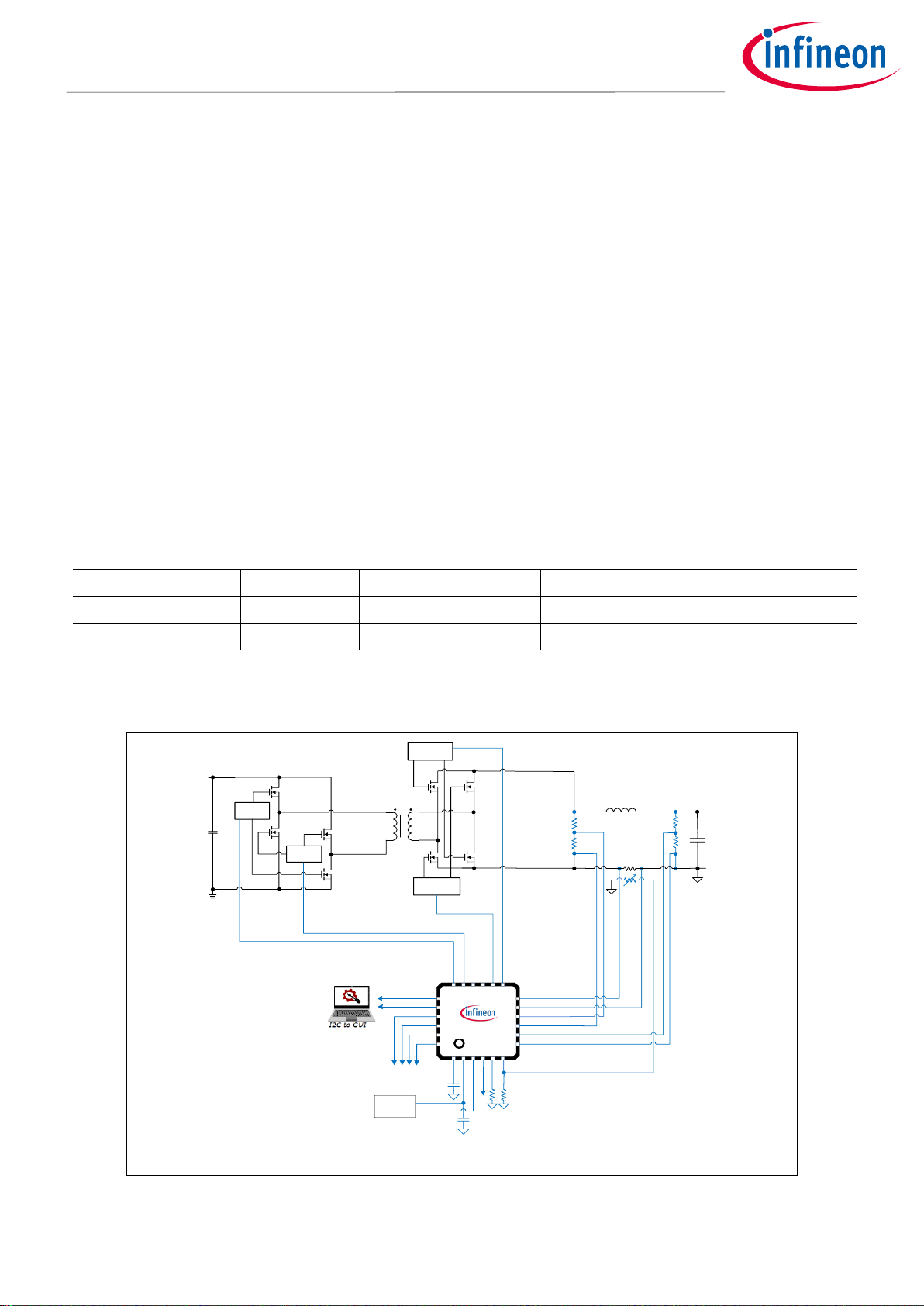
Figure 1 shows a typical application implementation of the XDPP1100 device in an isolated full-bridge DC to DC
step down converter:
L
o
C
o
PCB
Copper
Isolated
Driver
Isolated
Driver
To System
Driver
Driver
+
-
NTC
VRECT
A
B
SRA
SRB
Aux
Power
VDD
VD12
PRISEN
PWRGD
PWM3
PWM1
PWM4
TSEN
PWM2
SDA
SCL
EN
XADDR1
SMBALERT#
VREF
VRREF
VRSEN
ISEN
IREF
VSEN
IMON
XDPP1100-Q02 4
SYNC
PWM5
PWM6
V
IN
V
OUT
Figure 1 Typical application diagram

Datasheet 6 of 56 Revision 2.0
2020-11-20
XDPP1100
Digital power supply controller with PMBus interface & ARM CORTEX™ M0
Table of Contents
Table of Contents
Features ........................................................................................................................................ 1
Typical applications ........................................................................................................................ 3
Product validation .......................................................................................................................... 3
Ordering information ...................................................................................................................... 3
Description .................................................................................................................................... 4
Table of Contents ........................................................................................................................... 6
1 Functional Block Diagram ....................................................................................................... 8
2 Product Selection Matrix ......................................................................................................... 9
3 Terminal Configuration and Functions..................................................................................... 10
3.1 XDPP1100-Q040 Package ...................................................................................................................... 10
3.2 XDPP1100-Q024 Package ...................................................................................................................... 12
4 Specifications ....................................................................................................................... 14
4.1 Absolute Maximum Ratings .................................................................................................................. 14
4.2 Thermal Characteristics ........................................................................................................................ 14
4.3 Recommended Operating Conditions .................................................................................................. 15
4.4 Electrical Characteristics ...................................................................................................................... 15
5 Function Overview ................................................................................................................ 19
5.1 Introduction ........................................................................................................................................... 19
5.1.1 ARM® Cortex™ –M0 core ................................................................................................................... 19
5.1.2 Memories .......................................................................................................................................... 19
5.1.3 Communication ports ...................................................................................................................... 20
5.1.3.1 I2C/PMBus .................................................................................................................................... 20
5.1.3.2 UART ............................................................................................................................................ 20
5.1.3.3 Address offset .............................................................................................................................. 20
5.1.4 GPIO .................................................................................................................................................. 22
5.1.5 Register Map ..................................................................................................................................... 22
5.2 Analog Blocks and Subsystems ............................................................................................................ 23
5.2.1 Power Supply ................................................................................................................................... 23
5.2.2 Oscillator and PLL ............................................................................................................................ 23
5.2.3 Voltage Sense AFE1 .......................................................................................................................... 25
5.2.4 Current Sense AFE2 .......................................................................................................................... 27
5.2.5 General Purpose AFE3 ...................................................................................................................... 29
5.2.5.1 IMON and Active Current Sharing ............................................................................................... 30
5.2.5.2 Temperature sense ..................................................................................................................... 31
5.2.5.3 PRISEN ......................................................................................................................................... 32
5.3 Control Loop Subsystems ..................................................................................................................... 32
5.3.1 State diagram ................................................................................................................................... 32
5.3.2 Soft start ........................................................................................................................................... 33
5.3.3 Voltage Mode Control (VMC) ............................................................................................................ 34
5.3.4 Peak Current Mode Control (PCMC) ................................................................................................ 35
5.3.5 PID and Control Loops ..................................................................................................................... 36
5.3.6 Shutdown ......................................................................................................................................... 37
5.3.7 Current Sense Estimator .................................................................................................................. 37
5.3.8 Load-line (Droop) ............................................................................................................................. 38
5.3.9 Fast Transient Response .................................................................................................................. 38
5.3.10 Input Voltage Feedforward .............................................................................................................. 39

Datasheet 7 of 56 Revision 2.0
2020-11-20
XDPP1100
Digital power supply controller with PMBus interface & ARM CORTEX™ M0
Table of Contents
5.3.11 Current Balancing ............................................................................................................................ 40
5.3.12 Current Sharing ................................................................................................................................ 40
5.3.13 Flux Balancing .................................................................................................................................. 40
5.3.14 Burst Mode ....................................................................................................................................... 41
5.4 Protection and Fault ............................................................................................................................. 42
6 Application Information ......................................................................................................... 44
6.1 PWM full-bridge converter .................................................................................................................... 44
6.1.1 PWM full-bridge with center tapped output in VMC ....................................................................... 44
6.1.2 PWM full-bridge with PCMC ............................................................................................................. 45
6.2 PWM half-bridge converter ................................................................................................................... 46
6.3 Active clamp forward converter ........................................................................................................... 47
6.4 Interleaved Active Clamp Forward ....................................................................................................... 48
6.5 Dual-Loop converter ............................................................................................................................. 48
6.6 Non-isolated converter ......................................................................................................................... 49
6.7 Layout Guidelines .................................................................................................................................. 50
6.7.1 Component placement .................................................................................................................... 50
6.7.2 Routing ............................................................................................................................................. 51
6.7.3 Sense output current by copper trace ............................................................................................ 51
7 Package Information ............................................................................................................. 53
7.1 XDPP1100-Q024 QFN 4x4 – 24pin ......................................................................................................... 53
7.2 XDPP1100-Q040 QFN 6x6 – 40pin ......................................................................................................... 53
7.3 Part Marking .......................................................................................................................................... 54
Revision history............................................................................................................................. 55
Datasheet 8 of 56 Revision 2.0
2020-11-20
XDPP1100
Digital power supply controller with PMBus interface & ARM CORTEX™ M0
Functional Block Diagram
1 Functional Block Diagram
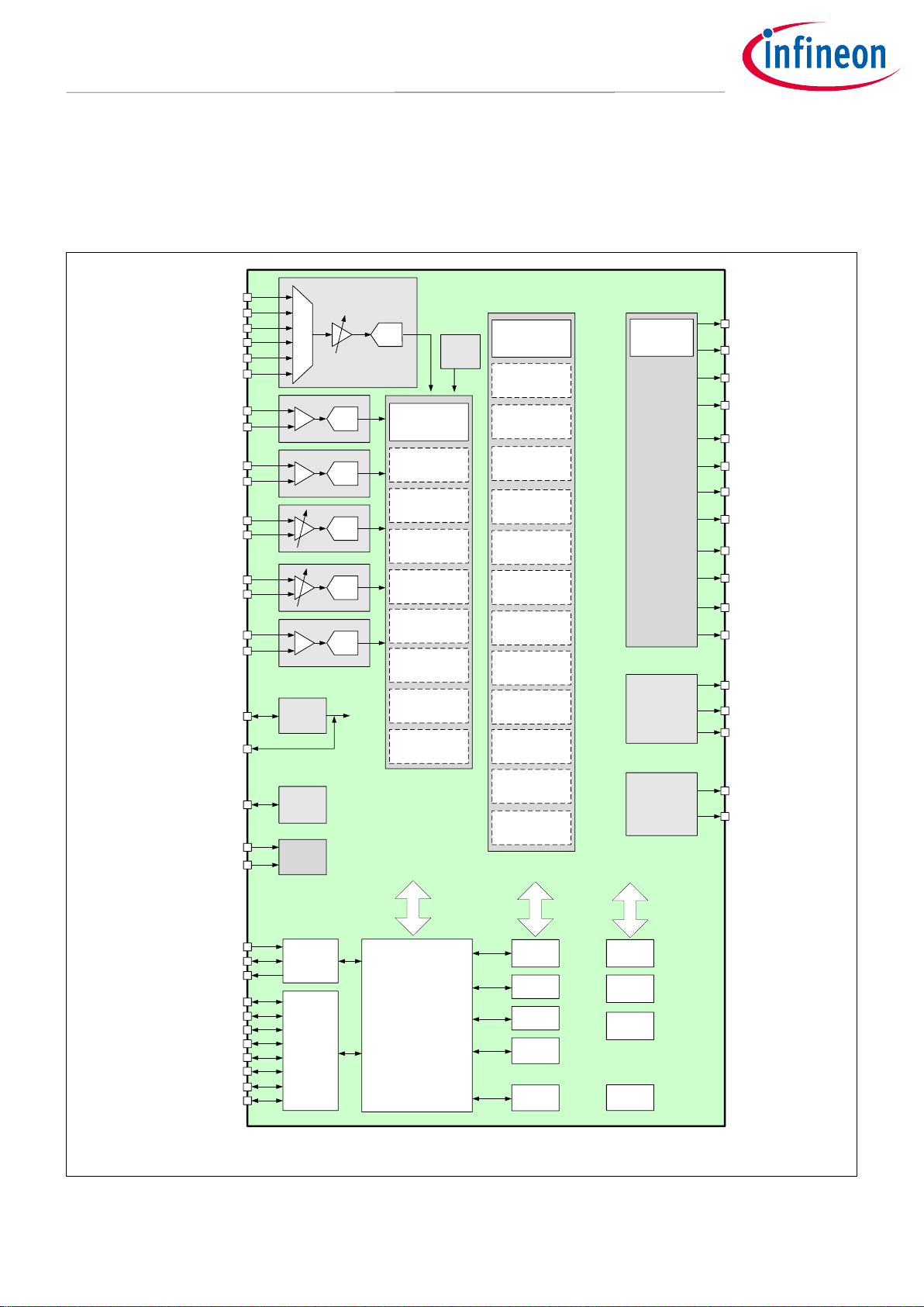
Figure 2 shows a functional block diagram of the XDPP1100 device architecture.
PWM
Generation
PWM6
ARM M0
AMBA BUS
Registers
I2C/
PMBUS
SCL
SDA
SMBALERT#
Analog
Resource
Configuration
Vout
Processor
PWM5
PWM7
ISEN
PWRGD
ADC
BTSEN
PRISEN
MUX
ADC
TSEN
PWM9
PWM8
PWM10
VSEN
ADC
PWM11
PWM12
VREF
AFE1
IREF
AFE2
VRSEN
BISEN
ADC
BIREF
AFE2
BVSEN_ BVRSEN
ADC
BVREF_BVRREF
AFE1
AFE3
OSC
PLL
XMER
Processor
Iout
Processor
Vin
Processor
Iin
Processor
Temp
Processor
Control
Configuration
Voltage Mode
Compensator
Current Mode
Compensator
Current
Protection
Current
Share
Light Load
Constant Power
Analog
BIST
Mode Control
Voltage Target
Sync Rec
Control
Flux
Balance
Voltage
Protection
I2C M/S
GPIO
(SDA2)
(SCL2)
FAULT1
POWER
MGR
BPWRGD
SYNC
LDO
CP
VDD
1.2V
RAM
DMA
ROM
OTP
BEN
Fault
Manager
Telemetry
Processor
Timers +
Counters
Interrupt
Manager
Math
PWM2
PWM1
PWM3
PWM4
MBIST
PWM
Configuration
POWER
MGR
EN
VD12
VDAC/IDAC
ADC
AFE1
VRREF
IMON
XADDR1
XADDR2
Internal
Temp
sensor
11-bit
11-bit
11-bit
9-bit
9-bit
9-bit
IMON
XADDR1
XADDR2
(FAN_PWM)
Blue pins: pins that are available in XDPP1100-Q040
(FAN_TACH)
(UARTRX)
FAULT2
(UARTTX)
Figure 2 Block diagram

Datasheet 9 of 56 Revision 2.0
2020-11-20
XDPP1100
Digital power supply controller with PMBus interface & ARM CORTEX™ M0
Product Selection Matrix
2 Product Selection Matrix
Table 4 Product selection table
FEATURE
XDPP1100-Q040
XDPP1100-Q024
ARM M0 core processor
100 MHz
100 MHz
High resolution DPWM outputs (78.125ps resolution)
12 6 Number of high-speed independent feedback rails
2 1 Number of voltage sense ADC
3 2 Number of current sense ADC
2
1
9-bit, 1Msps, general purpose ADC channels
6
4
OTP
64 kB
64 kB
RAM
32 kB
32 kB
ROM
80 kB
80 kB
DPWM switching frequency
Up to 2 MHz
Up to 2 MHz
Secondary serial bus ( I2C M/S)
Yes
No
UART
Yes
Yes
PMBus
Yes
Yes
Watchdog
Yes
Yes
On chip oscillator
Yes
Yes
Sync in and sync out functions
Yes
Yes
Temperature sense inputs
2
1
Enable inputs
2
1
Power good outputs
2 1 Total GPIO (General purpose I/O pins)
16
11
Package offering
VQFN-40 (6x6 mm2)
VQFN-24 (4x4 mm2)
Datasheet 10 of 56 Revision 2.0
2020-11-20
XDPP1100
Digital power supply controller with PMBus interface & ARM CORTEX™ M0
Terminal Configuration and Functions
3 Terminal Configuration and Functions
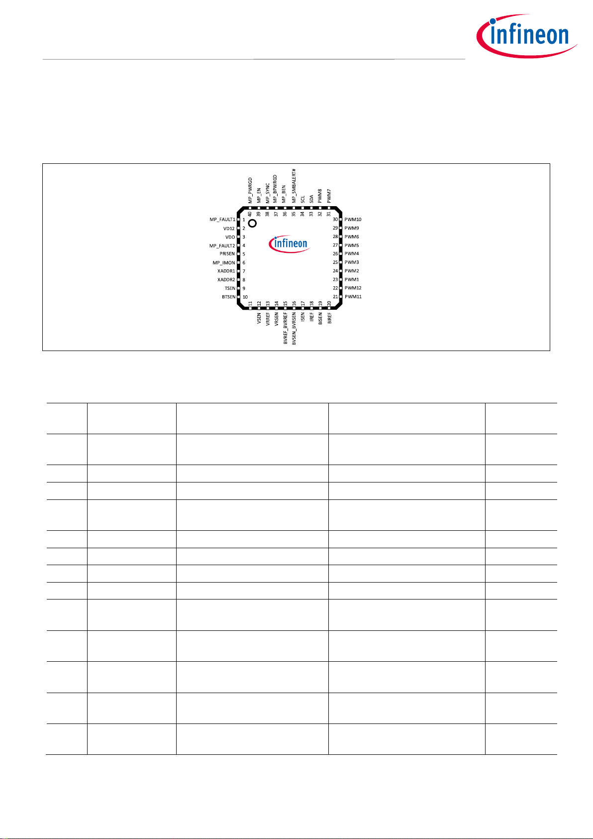
3.1 XDPP1100-Q040 Package
VREF
Figure 3 XDPP1100-Q040 pin assignment
Table 5 XDPP1100-Q040 pin definition
Pin No.
Name
Primary Assignment
Alternate assignment
Configurable
GPIO?
1
MP_FAULT1
Fault 1
SYNC/ FAN2_PWM/ SDA2/
UARTRX
Yes
2
VD12
1.2V supply bypass
3
VDD
3.3V main supply input
4
MP_FAULT2
Fault 2
SYNC/FAN2_TACH/ SCL2/
UARTTX
Yes
5
PRISEN
Primary voltage sensing input
GPA1
6
MP_IMON
Current monitor output
GPA2/ SYNC/ FAN1_TACH
Yes
7
XADDR1
Address 1
GPA3
8 XADDR2
Address 2
GPA4
9
TSEN
Temperature sensing input of
the first rail
GPA5
10
BTSEN
Temperature sensing input of
the second rail
GPA6
11
VREF
Differential voltage sensing of
the first rail, negative input
12
VSEN
Differential voltage sensing of
the first rail, positive input
13
VRREF
Transformer winding voltage
sense, negative input

Datasheet 11 of 56 Revision 2.0
2020-11-20
XDPP1100
Digital power supply controller with PMBus interface & ARM CORTEX™ M0
Terminal Configuration and Functions
Pin No.
Name
Primary Assignment
Alternate assignment
Configurable
GPIO?
14
VRSEN
Transformer winding voltage
sense or primary input voltage
sense, positive input
15
BVREF_BVRREF
Differential voltage sensing of
the second rail, negative input
Transformer winding voltage
sense return of the second rail
16
BVSEN_BVRSEN
Differential voltage sensing of
the second rail, positive input
Transformer winding voltage
sense of the second rail
17
ISEN
Differential current sensing of
the first rail, positive input
18
IREF
Differential current sensing of
the first rail, negative input
19
BISEN
Differential current sensing of
the second rail, positive input
20
BIREF
Differential current sensing of
the second rail, negative input
21
PWM11
PWM11 output
SYNC/ FAN1_PWM
Yes
22
PWM12
PWM12 output
SYNC/ FAN1_TACH
Yes
23
PWM1
PWM1 output
SYNC
Yes
24
PWM2
PWM2 output
SYNC
Yes
25
PWM3
PWM3 output
SYNC
Yes
26
PWM4
PWM4 output
SYNC
Yes
27
PWM5
PWM5 output
SYNC/ UARTRX
Yes
28
PWM6
PWM6 output
SYNC/ UARTTX
Yes
29
PWM9
PWM9 output
SYNC
Yes
30
PWM10
PWM10 output
SYNC
Yes
31
PWM7
PWM7 output
SYNC/ FAN2_PWM
Yes
32
PWM8
PWM8 output
SYNC/ FAN2_TACH
Yes
33
SDA
I2C serial data line
34
SCL
I2C serial clock line
35
MP_SMBALERT#
PMBus alert
SYNC
Yes
36
MP_BEN
Enable input of the second rail
SYNC/ SDA2/ UARTRX
Yes
37
MP_BPWRGD
Power good output of the
second rail
SYNC / SCL2/ UARTTX
Yes
38
MP_SYNC
Synchronize pin
FAN1_PWM
Yes
39
MP_EN
Enable input of the first rail
SYNC
Yes
40
MP_PWRGD
Power good output of the first
rail
SYNC
Yes
GND
Ground pin
Note: GND is the metal pad under the chip

Datasheet 12 of 56 Revision 2.0
2020-11-20
XDPP1100
Digital power supply controller with PMBus interface & ARM CORTEX™ M0
Terminal Configuration and Functions
3.2 XDPP1100-Q024 Package
1
2
3
4
5
6
7
8
9
20
19
18
17
16
15
14
13
12
11
21
22
23
24
10
PRISEN
IMON
XADDR1
TSEN
VDD
VD12
ISEN
IREF
VREF
VRSEN
VSEN
VRREF
PWM2
PWM1
PWM4
PWM3
SDA
SCL
MP_EN
MP_PWRGD
MP_SYNC
MP_SMBALERT
#
PWM6
PWM5
Figure 4 XDPP1100-Q024 pin assignment
Table 6 XDPP1100-Q024 pin definition
Pin No.
Name
Primary Assignment
Alternate assignment
Configurable
GPIO?
1
VD12
1.2V supply bypass
2
VDD
3.3V main supply input
3
PRISEN
Primary voltage sensing input
GPA1
4
MP_IMON
Output current monitor
GPA2/ SYNC/ FAN1_TACH
Yes 5 XADDR1
Address 1
GPA3
6 TSEN
Temperature sensing input
GPA4
7
VREF
Differential voltage sensing,
negative input
8
VSEN
Differential voltage sensing,
positive input
9
VRREF
Transformer winding voltage
sense, negative input
10
VRSEN
Transformer winding voltage
sense or primary input voltage
sense, positive input
11
ISEN
Differential current sensing,
positive input
12
IREF
Differential current sensing,
negative input
13
PWM1
PWM1 output
SYNC
Yes
14
PWM2
PWM2 output
SYNC
Yes
15
PWM3
PWM3 output
SYNC
Yes
16
PWM4
PWM4 output
SYNC
Yes
Datasheet 13 of 56 Revision 2.0
2020-11-20
XDPP1100
Digital power supply controller with PMBus interface & ARM CORTEX™ M0
Terminal Configuration and Functions
Pin No.
Name
Primary Assignment
Alternate assignment
Configurable
GPIO?
17
PWM5
PWM5 output
SYNC/ UARTRX
Yes
18
PWM6
PWM6 output
SYNC/ UARTTX
Yes
19
SDA
I2C serial data line
20
SCL
I2C serial clock line
21
MP_SMBALERT#
PMBus alert
SYNC
Yes
22
MP_SYNC
Synchronize pin
FAN1_PWM
Yes
23
MP_EN
Enable input
SYNC
Yes
24
MP_PWRGD
Power good output
SYNC
Yes GND
Ground pin
Note:
1. GND is the metal pad under the chip
2. NC: no connection pin
3. SDA and SCL are Open Drain I/O pins
4. All digital GPIO pins are 3.3V level CMOS, the outputs are programmable to be CMOS or Open Drain
Datasheet 14 of 56 Revision 2.0
2020-11-20
XDPP1100
Digital power supply controller with PMBus interface & ARM CORTEX™ M0
Specifications
4 Specifications
4.1 Absolute Maximum Ratings
Subjecting the controller to stresses above those listed in Table 7 Absolute Maximum Rating may cause
permanent damage to the device. These are absolute stress ratings only and functional operation of the device
is not implied or recommended at these or any other conditions in excess of those given in the Recommended
Operating Conditions sections of this specification. Exposure to absolute maximum ratings for extended
periods may adversely affect the operation and reliability of the device.
Table 7 Absolute maximum rating
Parameters
Symbol
Min.
Max.
Units
Remarks
VDD Supply Voltage
VDD
-0.3
4
V
Instantaneous voltage, see Note
3.7
V
Continuous voltage
VSEN, VRSEN, BVSEN_BVRSEN
-0.3
3.7*
V
*The lesser of 3.7V or VDD+0.2V
VREF, VRREF, BVREF_BVRREF
-0.3
0.5
V
ISEN, BISEN, IREF, BIREF
-0.3
3.7*
V
*The lesser of 3.7V or VDD+0.2V
-0.3
2.0
V
IPS mode
1.2V Supply
V
D12
-1 1 mA
All other pins
-0.3
3.7*
V
*The lesser of 3.7V or VDD+0.2V
Operating Junction Temperature
TJ
-40
150
°C
Storage Temperature
TS
-65
150
°C
Note: The absolute maximum VDD supply voltage is 4.0V with the conditions that the junction
temperature range is maintained between -40˚C < TJ < +125˚C and the product is not operated at
the absolute maximum VDD supply voltage for more than 24 hours cumulatively over the lifetime
of the product.
4.2 Thermal Characteristics
Table 8 Thermal Impedance
Parameters
Symbol
Value
Units
Remarks
Thermal Resistance, Junction to
Ambient, at 0 lfm
R
θJA
30.3
°C/W
QFN-40 6x6
53.5
QFN-24 4x4
Thermal Resistance, Junction to
Ambient, at 200 lfm
R
θJA
26.2
QFN-40 6x6
36.9
QFN-24 4x4
Thermal Resistance, Junction to
Ambient, at 500 lfm
R
θJA
23.4
QFN-40 6x6
30.3
QFN-24 4x4
Thermal Resistance, Junction to
Case (top)
R
θJC
2.8
QFN-40 6x6
3.7
QFN-24 4x4
Datasheet 15 of 56 Revision 2.0
2020-11-20
XDPP1100
Digital power supply controller with PMBus interface & ARM CORTEX™ M0
Specifications
4.3 Recommended Operating Conditions
For proper operation the device should be used within the recommended conditions.
Table 9 Recommended operating conditions
Parameters
Symbol
Min.
Nom.
Max.
Units
Remarks
Supply Voltage
VDD
3
3.3
3.6
V
Junction Temperature
TJ -40
25
125
°C
4.4 Electrical Characteristics
VDD=3.0 V to 3.6 V, 1 µF capacitor from VD12 to GND, TJ = -40 °C to 125 °C unless otherwise specified.
Table 10 Electrical characteristics of power supply section
Parameters
Symbol
Min.
Typ.
Max.
Units
Remarks
Supply current
I
DD0
11
16.5
mA
Both loops in off mode
Supply current
I
DD1
21
Single-loop operation, 4
PWMs switching at 250 kHz
without any load
Supply current
I
DD2
24
Dual-loop operation, all 12
PWMs switching at 250 kHz
without any load
VDD UVLO threshold
V
DD rising
2.78
2.95
V
V
DD falling
2.5
2.7
VDD UVLO hysteresis
80 mV
Table 11 Voltage ADC AFE1 section
Parameters
Symbol
Min.
Typ.
Max.
Units
Remarks
Input differential voltage range
0.25 2.1
V
Voltage below 0.5 V is not
production tested
Error voltage digital resolution
1.25 mV
Input impedance
REA
> 1 MΩ
Sample rate
100 MHz
VS ADC Accuracy (Note 5)
-1
±0.75 1 %
Setpoint 1.2 V to 2.1 V,
-40 °C <TA < 125 °C, 3.0 V <
VDD < 3.6 V, Typ = 3 σ
-1.4
±1.0
1.4
%
Setpoint 1.0 V,
-40 °C <TA < 125 °C, 3.0 V <
VDD < 3.6 V, Typ = 3 σ
-1.8
±1.2
1.8
%
Setpoint 0.8 V,
-40 °C <TA < 125 °C, 3.0 V <
VDD < 3.6 V, Typ = 3 σ
±0.45
%
Setpoint 1.2 V to 2.1 V,
TA = 25 °C, VDD = 3.3 V, Typ =
3 σ
Datasheet 16 of 56 Revision 2.0
2020-11-20
XDPP1100
Digital power supply controller with PMBus interface & ARM CORTEX™ M0
Specifications
Parameters
Symbol
Min.
Typ.
Max.
Units
Remarks
±0.65
%
Setpoint 1.0 V,
TA = 25 °C, VDD = 3.3 V, Typ =
3 σ
±0.9 %
Setpoint 0.8 V,
TA = 25 °C, VDD = 3.3 V, Typ =
3 σ
±10.5
mV
Setpoint 0.25 V to 0.5 V,
-40 °C <TA < 125 °C, 3.0 V <
VDD < 3.6 V, Typ = 3 σ
Table 12 Current ADC AFE2 section (high gain)
Parameters
Symbol
Min.
Typ.
Max.
Units
Remarks
Input differential voltage range
-22 22
mV
Voltage below -3 mV is not
production tested
Error voltage digital resolution
100 µV
Input impedance
REA
> 1 MΩ
IS ADC Offset
V
OFFSET
-4 4
LSB
Sample rate
25 MHz
IS ADC accuracy
-4
±2.7 4 %
11 mV differential input,
Typ = 3 σ
-3.5
±2.4
3.5
%
22 mV differential input,
Typ = 3 σ
Table 13 Current ADC AFE2 section (low gain)
Parameters
Symbol
Min.
Typ.
Max.
Units
Remarks
Input differential voltage range
-280 395
mV
Voltage below -50 mV is
not production tested
Error voltage digital resolution
1.45 mV
Input impedance
REA
> 1 MΩ
IS ADC Offset
V
OFFSET
-2.5 2.5
LSB
Sample rate
25 MHz
IS ADC accuracy
-3
±1.5 3 %
200 mV differential input,
Typ = 3 σ
-2
±1.2 2 %
395 mV differential input,
Typ = 3 σ
Table 14 Current ADC AFE2 section (IPS mode)
Parameters
Symbol
Min.
Typ.
Max.
Units
Remarks
Input common voltage range
1.11 1.3
V
Input differential voltage range
-200 425
mV
Voltage below -50 mV is
not production tested
Error voltage digital resolution
1.45 mV
Input impedance
REA
> 1 MΩ
IS ADC Offset
V
OFFSET
-2.5 2.5
LSB
Sample rate
25 MHz
Datasheet 17 of 56 Revision 2.0
2020-11-20
XDPP1100
Digital power supply controller with PMBus interface & ARM CORTEX™ M0
Specifications
Parameters
Symbol
Min.
Typ.
Max.
Units
Remarks
IS ADC accuracy
-3
±1.4 3 %
200 mV differential input,
Typ = 3 σ
-1.7
±1.1
1.7
%
395 mV differential input,
Typ = 3 σ
Table 15 General ADC AFE3 section
Parameters
Symbol
Min.
Typ.
Max.
Units
Remarks
Input differential voltage range
0 – 1.2 V
Error voltage digital resolution
2.344
mV
Input impedance
REA
> 1 MΩ
TS ADC offset error
V
OFFSET
-2 2
LSB
Sample rate
1 MHz
TS ADC Gain error
-1 1
%
Table 16 IMON DAC section
Parameters
Symbol
Min.
Typ.
Max.
Units
Remarks
Output current range
0-640 µA
Output current resolution
10 µA
TSIDAC accuracy
-3 3
%
Tested at 100 µA
Table 17 XADDR1, XADDR2 pins
Parameters
Symbol
Min.
Typ.
Max.
Units
Remarks
Current measurement
0-640 µA
Table 18 GPIO Inputs/Outputs
Parameters
Symbol
Min.
Typ.
Max.
Units
Remarks
Low-level output voltage
VOL
0.4
V
IOL = 5 mA
High-level output voltage
VOH
2.6
IOH = -5 mA
Low-level input voltage
VIL
1.0
High-level input voltage
VIH
2.3
Leakage current
IOZ
-1 1
µA
Table 19 SDA, SCL, SMBALERT pins
Parameters
Symbol
Min.
Typ.
Max.
Units
Remarks
Output low voltage
VOL
0.4
V
IOL = 20 mA
Low-level input voltage
VIL
1.0
Configured as 3.3V buffer
High-level input voltage
VIH
2.3
Low-level input voltage
VIL
0.6
Configured as 1.8V buffer
High-level input voltage
VIH
1.4
Leakage current
IOZ
-1 1
µA
Pin capacitance
C
PIN
1.5 pF
Table 20 System performance
Parameters
Symbol
Min.
Typ.
Max.
Units
Remarks
Processor master clock
100 MHz
 Loading...