


Data Sheet, V1.2, March 2006
XC167CI-16F
16-Bit Single-Chip Microcontroller
with C166SV2 Core
Microcontrollers

Edition 2006-03
Published by
Infineon Technologies AG
81726 München, Germany
© Infineon Technologies AG 2006.
All Rights Reserved.
Legal Disclaimer
The information given in this document shall in no event be regarded as a guarantee of conditions or
characteristics (“Beschaffenheitsgarantie”). With respect to any examples or hints given herein, any typical values
stated herein and/or any information regarding the application of the device, Infineon Technologies hereby
disclaims any and all warranties and liabilities of any kind, including without limitation warranties of noninfringement of intellectual property rights of any third party.
Information
For further information on technology, delivery terms and conditions and prices please contact your nearest
Infineon Technologies Office (www.infineon.com).
Warnings
Due to technical requirements components may contain dangerous substances. For information on the types in
question please contact your nearest Infineon Technologies Office.
Infineon Technologies Components may only be used in life-support devices or systems with the express written
approval of Infineon Technologies, if a failure of such components can reasonably be expected to cause the failure
of that life-support device or system, or to affect the safety or effectiveness of that device or system. Life support
devices or systems are intended to be implanted in the human body, or to support and/or maintain and sustain
and/or protect human life. If they fail, it is reasonable to assume that the health of the user or other persons may
be endangered.

Data Sheet, V1.2, March 2006
XC167CI-16F
16-Bit Single-Chip Microcontroller
with C166SV2 Core
Microcontrollers

XC167-16
Derivatives
XC167
Revision History: V1.2, 2006-03
Previous Version(s):
V1.1, 2003-06
V1.0, 2002-10
Page Subjects (major changes since last revision)
all Layout of graphics and text structures has been adapted to the new
company documentation rules.
73 Minimum oscillator period corrected
77 Output delay/hold time of A23 … A16 moved from
tc
-> tc12, tc21 -> tc
11
82 Parameter tc40 corrected
85 Chapter “Package and Reliability” added.
We Listen to Your Comments
Any information within this document that you feel is wrong, unclear or missing at all?
Your feedback will help us to continuously improve the quality of this document.
Please send your proposal (including a reference to this document) to:
mcdocu.comments@infineon.com
23
Data Sheet V1.2, 2006-03

XC167-16
Derivatives
Table of Contents
Table of Contents
1 Summary of Features . . . . . . . . . . . . . . . . . . . . . . . . . . . . . . . . . . . . . . . . 4
2 General Device Information . . . . . . . . . . . . . . . . . . . . . . . . . . . . . . . . . . . 7
2.1 Introduction . . . . . . . . . . . . . . . . . . . . . . . . . . . . . . . . . . . . . . . . . . . . . . . . . 7
2.2 Pin Configuration and Definition . . . . . . . . . . . . . . . . . . . . . . . . . . . . . . . . . 8
3 Functional Description . . . . . . . . . . . . . . . . . . . . . . . . . . . . . . . . . . . . . . 21
3.1 Memory Subsystem and Organization . . . . . . . . . . . . . . . . . . . . . . . . . . . . 22
3.2 External Bus Controller . . . . . . . . . . . . . . . . . . . . . . . . . . . . . . . . . . . . . . . 24
3.3 Central Processing Unit (CPU) . . . . . . . . . . . . . . . . . . . . . . . . . . . . . . . . . 26
3.4 Interrupt System . . . . . . . . . . . . . . . . . . . . . . . . . . . . . . . . . . . . . . . . . . . . 28
3.5 On-Chip Debug Support (OCDS) . . . . . . . . . . . . . . . . . . . . . . . . . . . . . . . 33
3.6 Capture/Compare Units (CAPCOM1/2) . . . . . . . . . . . . . . . . . . . . . . . . . . . 34
3.7 The Capture/Compare Unit CAPCOM6 . . . . . . . . . . . . . . . . . . . . . . . . . . . 37
3.8 General Purpose Timer (GPT12E) Unit . . . . . . . . . . . . . . . . . . . . . . . . . . . 38
3.9 Real Time Clock . . . . . . . . . . . . . . . . . . . . . . . . . . . . . . . . . . . . . . . . . . . . 42
3.10 A/D Converter . . . . . . . . . . . . . . . . . . . . . . . . . . . . . . . . . . . . . . . . . . . . . . 44
3.11 Asynchronous/Synchronous Serial Interfaces (ASC0/ASC1) . . . . . . . . . . 45
3.12 High Speed Synchronous Serial Channels (SSC0/SSC1) . . . . . . . . . . . . 46
3.13 TwinCAN Module . . . . . . . . . . . . . . . . . . . . . . . . . . . . . . . . . . . . . . . . . . . . 47
3.14 IIC Bus Module . . . . . . . . . . . . . . . . . . . . . . . . . . . . . . . . . . . . . . . . . . . . . 48
3.15 Watchdog Timer . . . . . . . . . . . . . . . . . . . . . . . . . . . . . . . . . . . . . . . . . . . . 49
3.16 Clock Generation . . . . . . . . . . . . . . . . . . . . . . . . . . . . . . . . . . . . . . . . . . . . 50
3.17 Parallel Ports . . . . . . . . . . . . . . . . . . . . . . . . . . . . . . . . . . . . . . . . . . . . . . . 50
3.18 Power Management . . . . . . . . . . . . . . . . . . . . . . . . . . . . . . . . . . . . . . . . . . 52
3.19 Instruction Set Summary . . . . . . . . . . . . . . . . . . . . . . . . . . . . . . . . . . . . . . 53
4 Electrical Parameters . . . . . . . . . . . . . . . . . . . . . . . . . . . . . . . . . . . . . . . 56
4.1 General Parameters . . . . . . . . . . . . . . . . . . . . . . . . . . . . . . . . . . . . . . . . . 56
4.2 DC Parameters . . . . . . . . . . . . . . . . . . . . . . . . . . . . . . . . . . . . . . . . . . . . . 59
4.3 Analog/Digital Converter Parameters . . . . . . . . . . . . . . . . . . . . . . . . . . . . 65
4.4 AC Parameters . . . . . . . . . . . . . . . . . . . . . . . . . . . . . . . . . . . . . . . . . . . . . 68
4.4.1 Definition of Internal Timing . . . . . . . . . . . . . . . . . . . . . . . . . . . . . . . . . . 68
4.4.2 On-chip Flash Operation . . . . . . . . . . . . . . . . . . . . . . . . . . . . . . . . . . . . 72
4.4.3 External Clock Drive XTAL1 . . . . . . . . . . . . . . . . . . . . . . . . . . . . . . . . . 73
4.4.4 Testing Waveforms . . . . . . . . . . . . . . . . . . . . . . . . . . . . . . . . . . . . . . . . 74
4.4.5 External Bus Timing . . . . . . . . . . . . . . . . . . . . . . . . . . . . . . . . . . . . . . . . 75
5 Package and Reliability . . . . . . . . . . . . . . . . . . . . . . . . . . . . . . . . . . . . . . 85
5.1 Packaging . . . . . . . . . . . . . . . . . . . . . . . . . . . . . . . . . . . . . . . . . . . . . . . . . 85
5.2 Flash Memory Parameters . . . . . . . . . . . . . . . . . . . . . . . . . . . . . . . . . . . . 86
Data Sheet 3 V1.2, 2006-03

XC16716-Bit Single-Chip Microcontroller with C166SV2 Core
XC166 Family
1 Summary of Features
• High Performance 16-bit CPU with 5-Stage Pipeline
– 25 ns Instruction Cycle Time at 40 MHz CPU Clock (Single-Cycle Execution)
– 1-Cycle Multiplication (16 ×16 bit), Background Division (32 / 16 bit) in 21 Cycles
– 1-Cycle Multiply-and-Accumulate (MAC) Instructions
– Enhanced Boolean Bit Manipulation Facilities
– Zero-Cycle Jump Execution
– Additional Instructions to Support HLL and Operating Systems
– Register-Based Design with Multiple Variable Register Banks
– Fast Context Switching Support with Two Additional Local Register Banks
– 16 Mbytes Total Linear Address Space for Code and Data
– 1024 Bytes On-Chip Special Function Register Area (C166 Family Compatible)
• 16-Priority-Level Interrupt System with 77 Sources, Sample-Rate down to 50 ns
• 8-Channel Interrupt-Driven Single-Cycle Data Transfer Facilities via
Peripheral Event Controller (PEC), 24-Bit Pointers Cover Total Address Space
• Clock Generation via on-chip PLL (factors 1:0.15 … 1:10), or
via Prescaler (factors 1:1 … 60:1)
• On-Chip Memory Modules
– 2 Kbytes On-Chip Dual-Port RAM (DPRAM)
– 4 Kbytes On-Chip Data SRAM (DSRAM)
– 2 Kbytes On-Chip Program/Data SRAM (PSRAM)
– 128 Kbytes On-Chip Program Memory (Flash Memory)
• On-Chip Peripheral Modules
– 16-Channel A/D Converter with Programmable Resolution (10-bit or 8-bit) and
Conversion Time (down to 2.55 µs or 2.15 µs)
– Two 16-Channel General Purpose Capture/Compare Units (32 Input/Output Pins)
– Capture/Compare Unit for flexible PWM Signal Generation (CAPCOM6)
(3/6 Capture/Compare Channels and 1 Compare Channel)
– Multi-Functional General Purpose Timer Unit with 5 Timers
– Two Synchronous/Asynchronous Serial Channels (USARTs)
– Two High-Speed-Synchronous Serial Channels
– On-Chip TwinCAN Interface (Rev. 2.0B active) with 32 Message Objects
(Full CAN/Basic CAN) on Two CAN Nodes, and Gateway Functionality
– IIC Bus Interface (10-bit addressing, 400 kbit/s) with 3 Channels (multiplexed)
– On-Chip Real Time Clock, Driven by Dedicated Oscillator
• Idle, Sleep, and Power Down Modes with Flexible Power Management
• Programmable Watchdog Timer and Oscillator Watchdog
Data Sheet 4 V1.2, 2006-03

Summary of Features
• Up to 12 Mbytes External Address Space for Code and Data
– Programmable External Bus Characteristics for Different Address Ranges
– Multiplexed or Demultiplexed External Address/Data Buses
– Selectable Address Bus Width
– 16-Bit or 8-Bit Data Bus Width
– Five Programmable Chip-Select Signals
– Hold- and Hold-Acknowledge Bus Arbitration Support
• Up to 103 General Purpose I/O Lines,
partly with Selectable Input Thresholds and Hysteresis
• On-Chip Bootstrap Loader
• Supported by a Large Range of Development Tools like C-Compilers,
Macro-Assembler Packages, Emulators, Evaluation Boards, HLL-Debuggers,
Simulators, Logic Analyzer Disassemblers, Programming Boards
• On-Chip Debug Support via JTAG Interface
• 144-Pin TQFP Package, 0.5 mm (19.7 mil) pitch
XC167-16
Derivatives
Ordering Information
The ordering code for Infineon microcontrollers provides an exact reference to the
required product. This ordering code identifies:
• the derivative itself, i.e. its function set, the temperature range, and the supply voltage
• the package and the type of delivery.
For the available ordering codes for the XC167 please refer to the “Product Catalog
Microcontrollers”, which summarizes all available microcontroller variants.
Note: The ordering codes for Mask-ROM versions are defined for each product after
verification of the respective ROM code.
This document describes several derivatives of the XC167 group. Table 1 enumerates
these derivatives and summarizes the differences. As this document refers to all of these
derivatives, some descriptions may not apply to a specific product.
For simplicity all versions are referred to by the term XC167 throughout this document.
Data Sheet 5 V1.2, 2006-03

Table 1 XC167 Derivative Synopsis
Derivative
1)
Temp.
Range
Program
Memory
XC167-16
Derivatives
Summary of Features
On-Chip RAM Interfaces
SAK-XC167CI-16F40F,
SAK-XC167CI-16F20F
-40 °C to
125 °C
128 Kbytes
Flash
2 Kbytes DPRAM,
4 Kbytes DSRAM,
2 Kbytes PSRAM
SAF-XC167CI-16F40F,
SAF-XC167CI-16F20F
-40 °C to
85 °C
128 Kbytes
Flash
2 Kbytes DPRAM,
4 Kbytes DSRAM,
2 Kbytes PSRAM
1) This Data Sheet is valid for devices starting with and including design step AD.
ASC0, ASC1,
SSC0, SSC1,
CAN0, CAN1,
IIC
ASC0, ASC1,
SSC0, SSC1,
CAN0, CAN1,
IIC
Data Sheet 6 V1.2, 2006-03
XC167-16
Derivatives
General Device Information
2 General Device Information
2.1 Introduction
The XC167 derivatives are high-performance members of the Infineon XC166 Family of
full featured single-chip CMOS microcontrollers. These devices extend the functionality
and performance of the C166 Family in terms of instructions (MAC unit), peripherals, and
speed. They combine high CPU performance (up to 40 million instructions per second)
with high peripheral functionality and enhanced IO-capabilities. They also provide clock
generation via PLL and various on-chip memory modules such as program Flash,
program RAM, and data RAM.
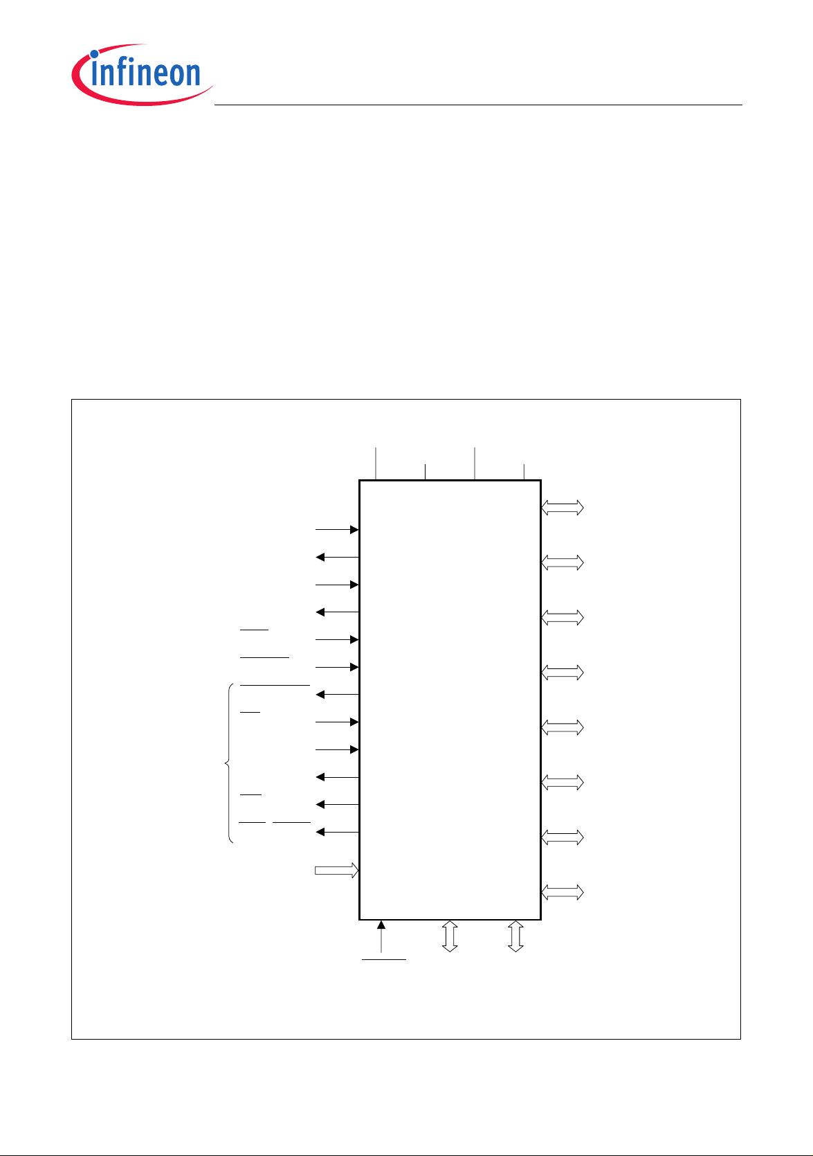
Port 20
6 bit
XTAL1
XTAL2
XTAL3
XTAL4
NMI
RSTIN
RSTOUT
EA
READY
ALE
RD
WR/WRL
Port 5
16 bit
V
AREF
V
AGND
XC167
V
DDI/P
V
SSI/P
PORT0
16 bit
PORT1
16 bit
Port 2
8 bit
Port 3
15 bit
Port 4
8 bit
Port 6
8 bit
Port 7
4 bit
Port 9
6 bit
TRST Debug
JTAG
5 bit
2 bit
MCA05554_7
Figure 1 Logic Symbol
Data Sheet 7 V1.2, 2006-03
XC167-16
Derivatives
General Device Information
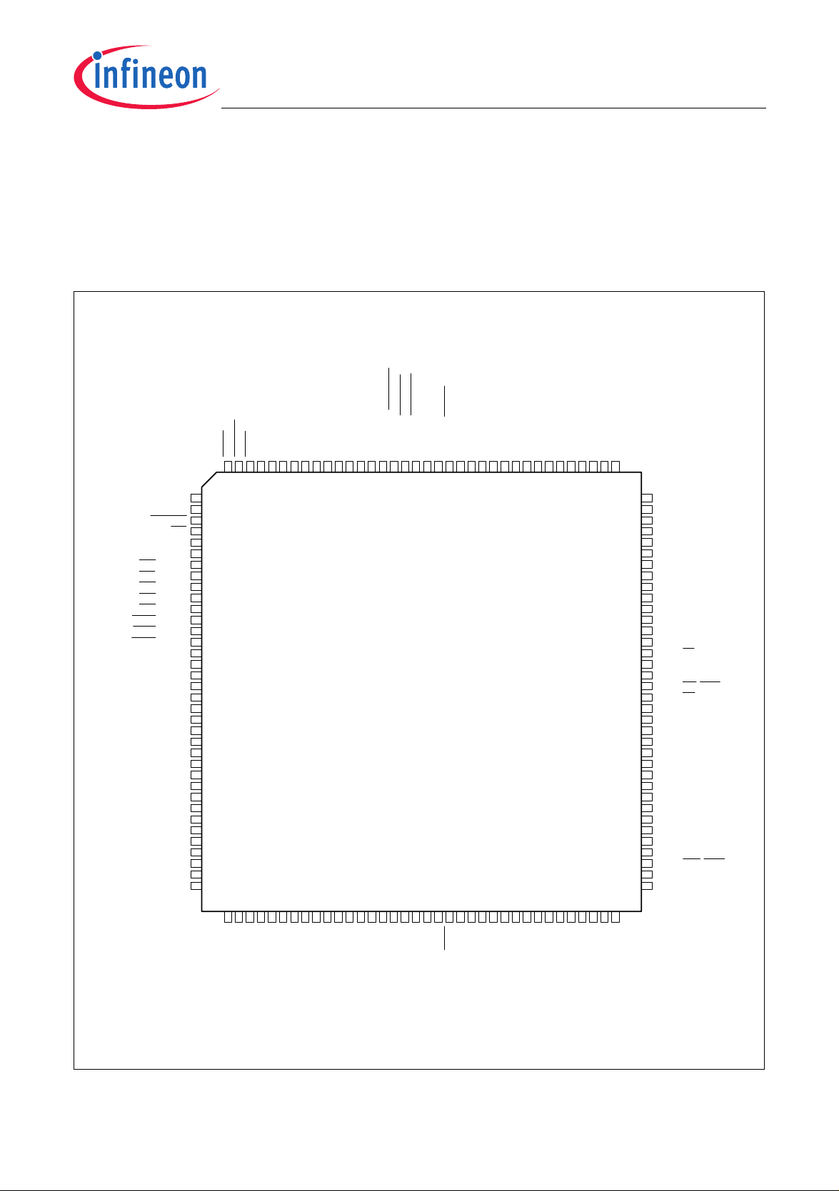
2.2 Pin Configuration and Definition
The pins of the XC167 are described in detail in Table 2, including all their alternate
functions. Figure 2 summarizes all pins in a condensed way, showing their location on
the 4 sides of the package. E*) and C*) mark pins to be used as alternate external
interrupt inputs, C*) marks pins that can have CAN interface lines assigned to them.
SSI
BRKIN
BRKOUT
RSTIN
XTAL4
XTAL3
SSIVDDI
V
XTAL1
XTAL2
V
P1H.7/A15/CC27IO
P1H.6/A14/CC26IO
P1H.5/A13/CC25IO
P1H.4/A12/CC24IO
P1H.3/A11/SCLK1/E*)
SSPVDDP
P1H.2/A10/CC6POS2/MTSR1
P1H.1/A9/CC6POS1/MRST1
P1H.0/A8/CC6POS0/CC23IO/E*)
V
P1L.7/A7/CTRAP/CC22IO
P1L.6/A6/COUT63
P1L.5/A5/COUT62
P1L.4/A4/CC62
P1L.3/A3/COUT61
P1L.2/A2/CC61
P1L.1/A1/COUT60
P1L.0/A0/CC60
P0H.7/AD15
P0H.6/AD14
P0H.5/AD13
P0H.4/AD12
P0H.3/AD11
P0H.2/AD10
N.C.
N.C.
N.C.
P20.12/RSTOUT
P6.0/CS0/CC0IO
P6.1/CS1/CC1IO
P6.2/CS2/CC2IO
P6.3/CS3/CC3IO
P6.4/CS4/CC4IO
P6.5/HOLD/CC5IO
P6.6/HLDA/CC6IO
P6.7/BREQ/CC7IO
P7.4/CC28IO/C*)
P7.5/CC29IO/C*)
P7.6/CC30IO/C*)
P7.7/CC31IO/C*)
P9.0/SDA0/CC16IO/C*)
P9.1/SCL0/CC17IO/C*)
P9.2/SDA1/CC18IO/C*)
P9.3/SCL1/CC19IO/C*)
P9.4/SDA2/CC20IO
P9.5/SCL2/CC21IO
P5.10/AN10/T6EUD
P5.11/AN11/T5EUD
N.C.
NMI
V
SSP
V
DDP
V
SSP
V
DDP
V
SSP
V
DDP
P5.0/AN0
P5.1/AN1
P5.2/AN2
P5.3/AN3
P5.4/AN4
P5.5/AN5
144
143
142
141
140
139
138
137
136
135
134
133
132
131
130
129
128
127
126
125
124
123
122
121
120
119
118
117
116
1
2
3
4
5
6
7
8
9
10
11
12
13
14
15
16
17
18
19
20
21
22
23
24
25
26
27
28
29
30
31
32
33
34
35
3738394041424344454647484950515253545556575859606162636465666768697071
XC167
115
114
113
112
111
110
109
N.C.
108
N.C.
107
P0H.1/AD9
106
P0H.0/AD8
105
V
104
SSP
V
103
DDP
P0L.7/AD7
102
P0L.6/AD6
101
P0L.5/AD5
100
P0L.4/AD4
99
P0L.3/AD3
98
P0L.2/AD2
97
P0L.1/AD1
96
P0L.0/AD0
95
P20.5/EA
94
P20.4/ALE
93
P20.2/READY
92
P20.1/WR/WRL
91
P20.0/RD
90
V
89
SSP
V
88
DDP
P4.7/A23/C*)
87
P4.6/A22/C*)
86
P4.5/A21/C*)
85
P4.4/A20/C*)
84
P4.3/A19
83
P4.2/A18
82
P4.1/A17
81
P4.0/A16
80
V
79
SSI
V
78
DDI
P3.15/CLKOUT/FOUT
77
P3.13/SCLK0/E*)
76
P3.12/BHE/WRH/E*)
75
TMS
74
TDO
7336
72
SSI
P5.8/AN8
P5.9/AN9
P5.6/AN6
P5.7/AN7
DDI
AREF
AGND
V
V
V
V
P5.12/AN12/T6IN
P5.13/AN13/T5IN
P5.14/AN14/T4EUD
P2.8/CC8IO/EX0IN
P5.15/AN15/T2EUD
P2.9/CC9IO/EX1IN
P2.10/CC10IO/EX2IN
P2.11/CC11IO/EX3IN
P2.12/CC12IO/EX4IN
P2.13/CC13IO/EX5IN
DDP
V
TRST
P3.5/T4IN
P3.6/T3IN
P3.2/CAPIN
P3.3/T3OUT
P2.14/CC14IO/EX6IN
P3.0/T0IN/TxD1/E*)
P3.1/T6OUT/RxD1/E*)
P2.15/CC15IO/EX7IN/T7IN
P3.7/T2IN
P3.4/T3EUD
P3.8/MRST0
P3.9/MTSR0
TDI
TCK
P3.10/TxD0/E*)
P3.11/RxD0/E*)
MCP06458
Figure 2 Pin Configuration (top view)
Data Sheet 8 V1.2, 2006-03
Table 2 Pin Definitions and Functions
XC167-16
Derivatives
General Device Information
Symbol
Pin
Num.
Input
Outp.
Function
P20.12 3 IO For details, please refer to the description of P20.
NMI
4 I Non-Maskable Interrupt Input. A high to low transition at this
pin causes the CPU to vector to the NMI trap routine. When
the PWRDN (power down) instruction is executed, the NMI
pin must be low in order to force the XC167 into power down
mode. If NMI
is high, when PWRDN is executed, the part will
continue to run in normal mode.
P6
IO
If not used, pin NMI
Port 6 is an 8-bit bidirectional I/O port. Each pin can be
should be pulled high externally.
programmed for input (output driver in high-impedance
state) or output (configurable as push/pull or open drain
driver). The input threshold of Port 6 is selectable (standard
or special).
The Port 6 pins also serve for alternate functions:
P6.0
P6.1
P6.2
P6.3
P6.4
P6.5
P6.6
7
8
9
10
11
12
13
O
IO
O
IO
O
IO
O
IO
O
IO
I
IO
I/O
CS0
Chip Select 0 Output,
CC0IO CAPCOM1: CC0 Capture Inp./Compare Output
CS1
Chip Select 1 Output,
CC1IO CAPCOM1: CC1 Capture Inp./Compare Output
CS2
Chip Select 2 Output,
CC2IO CAPCOM1: CC2 Capture Inp./Compare Output
CS3
Chip Select 3 Output,
CC3IO CAPCOM1: CC3 Capture Inp./Compare Output
CS4
Chip Select 4 Output,
CC4IO CAPCOM1: CC4 Capture Inp./Compare Output
HOLD
External Master Hold Request Input,
CC5IO CAPCOM1: CC5 Capture Inp./Compare Output
HLDA
Hold Acknowledge Output (master mode) or
Input (slave mode),
CC6IO CAPCOM1: CC6 Capture Inp./Compare Output
BREQ
Bus Request Output,
CC7IO CAPCOM1: CC7 Capture Inp./Compare Output
P6.7
14
IO
O
IO
Data Sheet 9 V1.2, 2006-03

Table 2 Pin Definitions and Functions (cont’d)
XC167-16
Derivatives
General Device Information
Symbol
P7
P7.4
P7.5
P7.6
P7.7
Pin
Num.
15
16
17
18
Input
Outp.
IO
I/O
I
I
I/O
O
I
I/O
I
I
I/O
O
I
Function
Port 7 is a 4-bit bidirectional I/O port. Each pin can be
programmed for input (output driver in high-impedance
state) or output (configurable as push/pull or open drain
driver). The input threshold of Port 7 is selectable (standard
or special).
Port 7 pins provide inputs/outputs for CAPCOM2 and serial
interface lines.
1)
CC28IO CAPCOM2: CC28 Capture Inp./Compare Outp.,
CAN2_RxD CAN Node 2 Receive Data Input,
EX7IN Fast External Interrupt 7 Input (alternate pin B)
CC29IO CAPCOM2: CC29 Capture Inp./Compare Outp.,
CAN2_TxD CAN Node 2 Transmit Data Output,
EX6IN Fast External Interrupt 6 Input (alternate pin B)
CC30IO CAPCOM2: CC30 Capture Inp./Compare Outp.,
CAN1_RxD CAN Node 1 Receive Data Input,
EX7IN Fast External Interrupt 7 Input (alternate pin A)
CC31IO CAPCOM2: CC31 Capture Inp./Compare Outp.,
CAN1_TxD CAN Node 1 Transmit Data Output,
EX6IN Fast External Interrupt 6 Input (alternate pin A)
Data Sheet 10 V1.2, 2006-03

Table 2 Pin Definitions and Functions (cont’d)
XC167-16
Derivatives
General Device Information
Symbol
P9
P9.0
P9.1
P9.2
P9.3
P9.4
P9.5
Pin
Num.
21
22
23
24
25
26
Input
Outp.
IO
I/O
I
I/O
I/O
O
I/O
I/O
I
I/O
I/O
O
I/O
I/O
I/O
I/O
I/O
Function
Port 9 is a 6-bit bidirectional I/O port. Each pin can be
programmed for input (output driver in high-impedance
state) or output (configurable as push/pull or open drain
driver). The input threshold of Port 9 is selectable (standard
or special).
The following Port 9 pins also serve for alternate functions:
CC16IO CAPCOM2: CC16 Capture Inp./Compare Outp.,
CAN2_RxD CAN Node 2 Receive Data Input,
SDA0 IIC Bus Data Line 0
CC17IO CAPCOM2: CC17 Capture Inp./Compare Outp.,
CAN2_TxD CAN Node 2 Transmit Data Output,
SCL0 IIC Bus Clock Line 0
CC18IO CAPCOM2: CC18 Capture Inp./Compare Outp.,
CAN1_RxD CAN Node 1 Receive Data Input,
SDA1 IIC Bus Data Line 1
CC19IO CAPCOM2: CC19 Capture Inp./Compare Outp.,
CAN1_TxD CAN Node 1 Transmit Data Output,
SCL1 IIC Bus Clock Line 1
CC20IO CAPCOM2: CC20 Capture Inp./Compare Outp.,
SDA2 IIC Bus Data Line 2
CC21IO CAPCOM2: CC21 Capture Inp./Compare Outp.,
SCL2 IIC Bus Clock Line 2
1)
Data Sheet 11 V1.2, 2006-03

Table 2 Pin Definitions and Functions (cont’d)
XC167-16
Derivatives
General Device Information
Symbol
P5
P5.0
P5.1
P5.2
P5.3
P5.4
P5.5
P5.10
P5.11
P5.8
P5.9
P5.6
P5.7
P5.12
P5.13
P5.14
P5.15
Pin
Num.
29
30
31
32
33
34
35
36
37
38
39
40
43
44
45
46
Input
Outp.
I
I
I
I
I
I
I
I
I
I
I
I
I
I
I
I
I
Function
Port 5 is a 16-bit input-only port.
The pins of Port 5 also serve as analog input channels for the
A/D converter, or they serve as timer inputs:
AN0
AN1
AN2
AN3
AN4
AN5
AN10, T6EUD GPT1 Timer T4 Ext. Up/Down Ctrl. Inp.
AN11, T5EUD GPT1 Timer T2 Ext. Up/Down Ctrl. Inp
AN8
AN9
AN6
AN7
AN12, T6IN GPT2 Timer T6 Count/Gate Input
AN13, T5IN GPT2 Timer T5 Count/Gate Input
AN14, T4EUD GPT1 Timer T4 Ext. Up/Down Ctrl. Inp.
AN15, T2EUD GPT1 Timer T2 Ext. Up/Down Ctrl. Inp.
Data Sheet 12 V1.2, 2006-03

Table 2 Pin Definitions and Functions (cont’d)
XC167-16
Derivatives
General Device Information
Symbol
P2
P2.8
P2.9
P2.10
P2.11
P2.12
P2.13
P2.14
P2.15
Pin
Num.
49
50
51
52
53
54
55
56
Input
Outp.
IO
I/O
I
I/O
I
I/O
I
I/O
I
I/O
I
I/O
I
I/O
I
I/O
I
I
Function
Port 2 is an 8-bit bidirectional I/O port. Each pin can be
programmed for input (output driver in high-impedance
state) or output (configurable as push/pull or open drain
driver). The input threshold of Port 2 is selectable (standard
or special).
The following Port 2 pins also serve for alternate functions:
CC8IO CAPCOM1: CC8 Capture Inp./Compare Output,
EX0IN Fast External Interrupt 0 Input (default pin)
CC9IO CAPCOM1: CC9 Capture Inp./Compare Output,
EX1IN Fast External Interrupt 1 Input (default pin)
CC10IO CAPCOM1: CC10 Capture Inp./Compare Outp.,
EX2IN Fast External Interrupt 2 Input (default pin)
CC11IO CAPCOM1: CC11 Capture Inp./Compare Outp.,
EX3IN Fast External Interrupt 3 Input (default pin)
CC12IO CAPCOM1: CC12 Capture Inp./Compare Outp.,
EX4IN Fast External Interrupt 4 Input (default pin)
CC13IO CAPCOM1: CC13 Capture Inp./Compare Outp.,
EX5IN Fast External Interrupt 5 Input (default pin)
CC14IO CAPCOM1: CC14 Capture Inp./Compare Outp.,
EX6IN Fast External Interrupt 6 Input (default pin)
CC15IO CAPCOM1: CC15 Capture Inp./Compare Outp.,
EX7IN Fast External Interrupt 7 Input (default pin),
T7IN CAPCOM2: Timer T7 Count Input
TRST
57 I Test-System Reset Input. A high-level at this pin activates
the XC167’s debug system.
Note: For normal system operation, pin TRST
should be
held low.
Data Sheet 13 V1.2, 2006-03

Table 2 Pin Definitions and Functions (cont’d)
XC167-16
Derivatives
General Device Information
Symbol
P3
P3.0
P3.1
P3.2
P3.3
P3.4
P3.5
P3.6
P3.7
P3.8
P3.9
P3.10
P3.11
P3.12
P3.13
P3.15
Pin
Num.
59
60
61
62
63
64
65
66
67
68
69
70
75
76
77
Input
Outp.
IO
I
O
I
O
I/O
I
I
O
I
I
I
I
I/O
I/O
O
I
I/O
I
O
O
I
I/O
I
O
O
Function
Port 3 is a 15-bit bidirectional I/O port. Each pin can be
programmed for input (output driver in high-impedance
state) or output (configurable as push/pull or open drain
driver). The input threshold of Port 3 is selectable (standard
or special).
The following Port 3 pins also serve for alternate functions:
T0IN CAPCOM1 Timer T0 Count Input,
TxD1 ASC1 Clock/Data Output (Async./Sync),
EX1IN Fast External Interrupt 1 Input (alternate pin B)
T6OUT GPT2 Timer T6 Toggle Latch Output,
RxD1 ASC1 Data Input (Async.) or Inp./Outp. (Sync.),
EX1IN Fast External Interrupt 1 Input (alternate pin A)
CAPIN GPT2 Register CAPREL Capture Input
T3OUT GPT1 Timer T3 Toggle Latch Output
T3EUD GPT1 Timer T3 External Up/Down Control Input
T4IN GPT1 Timer T4 Count/Gate/Reload/Capture Inp
T3IN GPT1 Timer T3 Count/Gate Input
T2IN GPT1 Timer T2 Count/Gate/Reload/Capture Inp
MRST0 SSC0 Master-Receive/Slave-Transmit In/Out.
MTSR0 SSC0 Master-Transmit/Slave-Receive Out/In.
TxD0 ASC0 Clock/Data Output (Async./Sync.),
EX2IN Fast External Interrupt 2 Input (alternate pin B)
RxD0 ASC0 Data Input (Async.) or Inp./Outp. (Sync.),
EX2IN Fast External Interrupt 2 Input (alternate pin A)
BHE
WRH
External Memory High Byte Enable Signal,
External Memory High Byte Write Strobe,
EX3IN Fast External Interrupt 3 Input (alternate pin B)
SCLK0 SSC0 Master Clock Output/Slave Clock Input.,
EX3IN Fast External Interrupt 3 Input (alternate pin A)
CLKOUT Master Clock Output,
FOUT Programmable Frequency Output
TCK 71 I Debug System: JTAG Clock Input
TDI 72 I Debug System: JTAG Data In
TDO 73 O Debug System: JTAG Data Out
TMS 74 I Debug System: JTAG Test Mode Selection
Data Sheet 14 V1.2, 2006-03

Table 2 Pin Definitions and Functions (cont’d)
XC167-16
Derivatives
General Device Information
Symbol
P4
P4.0
P4.1
P4.2
P4.3
P4.4
P4.5
P4.6
P4.7
Pin
Num.
80
81
82
83
84
85
86
87
Input
Outp.
IO
O
O
O
O
O
I
I
O
I
I
O
O
I
O
I
O
I
Function
Port 4 is an 8-bit bidirectional I/O port. Each pin can be
programmed for input (output driver in high-impedance
state) or output (configurable as push/pull or open drain
driver). The input threshold of Port 4 is selectable (standard
or special).
Port 4 can be used to output the segment address lines, the
optional chip select lines, and for serial interface lines:
1)
A16 Least Significant Segment Address Line
A17 Segment Address Line
A18 Segment Address Line
A19 Segment Address Line
A20 Segment Address Line,
CAN2_RxD CAN Node 2 Receive Data Input,
EX5IN Fast External Interrupt 5 Input (alternate pin B)
A21 Segment Address Line,
CAN1_RxD CAN Node 1 Receive Data Input,
EX4IN Fast External Interrupt 4 Input (alternate pin B)
A22 Segment Address Line,
CAN1_TxD CAN Node 1 Transmit Data Output,
EX5IN Fast External Interrupt 5 Input (alternate pin A)
A23 Most Significant Segment Address Line,
CAN1_RxD CAN Node 1 Receive Data Input,
CAN2_TxD CAN Node 2 Transmit Data Output,
EX4IN Fast External Interrupt 4 Input (alternate pin A)
Data Sheet 15 V1.2, 2006-03
Table 2 Pin Definitions and Functions (cont’d)
XC167-16
Derivatives
General Device Information
Symbol
P20
P20.0
P20.1
P20.2
P20.4
P20.5
P20.12
Pin
Num.
90
91
92
93
94
3
Input
Outp.
IO
O
O
I
O
I
O
Function
Port 20 is a 6-bit bidirectional I/O port. Each pin can be
programmed for input (output driver in high-impedance
state) or output. The input threshold of Port 20 is selectable
(standard or special).
The following Port 20 pins also serve for alternate functions:
RD
External Memory Read Strobe, activated for
every external instruction or data read access.
WR
/WRL External Memory Write Strobe.
In WR
-mode this pin is activated for every
external data write access.
In WRL
-mode this pin is activated for low byte
data write accesses on a 16-bit bus, and for
every data write access on an 8-bit bus.
READY READY Input. When the READY function is
enabled, memory cycle time waitstates can be
forced via this pin during an external access.
ALE Address Latch Enable Output.
Can be used for latching the address into
external memory or an address latch in the
multiplexed bus modes.
EA
External Access Enable pin.
A low-level at this pin during and after Reset
forces the XC167 to latch the configuration from
PORT0 and pin RD
, and to begin instruction
execution out of external memory.
A high-level forces the XC167 to latch the
configuration from pins RD
, ALE, and WR, and
to begin instruction execution out of the internal
program memory. “ROMless” versions must
have this pin tied to ‘0’.
RSTOUT
Internal Reset Indication Output.
Is activated asynchronously with an external
hardware reset. It may also be activated
(selectable) synchronously with an internal
software or watchdog reset.
Is deactivated upon the execution of the EINIT
instruction, optionally at the end of reset, or at
any time (before EINIT) via user software.
Note: Port 20 pins may input configuration values (see EA
Data Sheet 16 V1.2, 2006-03
).

Table 2 Pin Definitions and Functions (cont’d)
XC167-16
Derivatives
General Device Information
Symbol
PORT0
P0L.0 P0L.7,
P0H.0,
P0H.1,
P0H.2 P0H.7
Pin
Num.
95 102,
105,
106,
111 116
Input
Function
Outp.
IO PORT0 consists of the two 8-bit bidirectional I/O ports P0L
and P0H. Each pin can be programmed for input (output
driver in high-impedance state) or output.
In case of an external bus configuration, PORT0 serves as
the address (A) and address/data (AD) bus in multiplexed
bus modes and as the data (D) bus in demultiplexed bus
modes.
Demultiplexed bus modes:
8-bit data bus: P0H = I/O, P0L = D7 - D0
16-bit data bus: P0H = D15 - D8, P0L = D7 - D0
Multiplexed bus modes:
8-bit data bus: P0H = A15 - A8, P0L = AD7 - AD0
16-bit data bus: P0H = AD15 - AD8, P0L = AD7 - AD0
Note: At the end of an external reset (EA
= 0) PORT0 also
may input configuration values.
Data Sheet 17 V1.2, 2006-03

Table 2 Pin Definitions and Functions (cont’d)
XC167-16
Derivatives
General Device Information
Symbol
PORT1
P1L.0
P1L.1
P1L.2
P1L.3
P1L.4
P1L.5
P1L.6
P1L.7
P1H.0
P1H.1
P1H.2
P1H.3
P1H.4
P1H.5
P1H.6
P1H.7
Pin
Num.
117
118
119
120
121
122
123
124
127
128
129
130
131
132
133
134
Input
Outp.
IO
I/O
O
I/O
O
I/O
O
O
I
I/O
I
I
I/O
I
I/O
I
I/O
I/O
I
I/O
I/O
I/O
I/O
Function
PORT1 consists of the two 8-bit bidirectional I/O ports P1L
and P1H. Each pin can be programmed for input (output
driver in high-impedance state) or output.
PORT1 is used as the 16-bit address bus (A) in
demultiplexed bus modes (also after switching from a
demultiplexed to a multiplexed bus mode).
The following PORT1 pins also serve for alt. functions:
CC60 CAPCOM6: Input / Output of Channel 0
COUT60 CAPCOM6: Output of Channel 0
CC61 CAPCOM6: Input / Output of Channel 1
COUT61 CAPCOM6: Output of Channel 1
CC62 CAPCOM6: Input / Output of Channel 2
COUT62 CAPCOM6: Output of Channel 2
COUT63 Output of 10-bit Compare Channel
CTRAP
CAPCOM2: CC22 Capture Inp./Compare Outp.
CTRAP
is an input pin with an internal pull-up
resistor. A low level on this pin switches the
CAPCOM6 compare outputs to the logic level
defined by software (if enabled).
CC22IO CAPCOM2: CC22 Capture Inp./Compare Outp.
CC6POS0
CAPCOM6: Position 0 Input,
EX0IN Fast External Interrupt 0 Input (alternate pin B),
CC23IO CAPCOM2: CC23 Capture Inp./Compare Outp.
CC6POS1
CAPCOM6: Position 1 Input,
MRST1 SSC1 Master-Receive/Slave-Transmit In/Out.
CC6POS2
CAPCOM6: Position 2 Input,
MTSR1 SSC1 Master-Transmit/Slave-Receive Out/Inp.
SCLK1 SSC1 Master Clock Output / Slave Clock Input,
EX0IN Fast External Interrupt 0 Input (alternate pin A)
CC24IO CAPCOM2: CC24 Capture Inp./Compare Outp.
CC25IO CAPCOM2: CC25 Capture Inp./Compare Outp.
CC26IO CAPCOM2: CC26 Capture Inp./Compare Outp.
CC27IO CAPCOM2: CC27 Capture Inp./Compare Outp.
Data Sheet 18 V1.2, 2006-03

Table 2 Pin Definitions and Functions (cont’d)
XC167-16
Derivatives
General Device Information
Symbol
XTAL2
XTAL1
XTAL3
XTAL4
RSTIN
Pin
Num.
137
138
Input
Outp.
O
I
Function
XTAL2: Output of the main oscillator amplifier circuit
XTAL1: Input to the main oscillator amplifier and input to
the internal clock generator
To clock the device from an external source, drive XTAL1,
while leaving XTAL2 unconnected. Minimum and maximum
high/low and rise/fall times specified in the AC
Characteristics must be observed.
140
141
I
O
XTAL3: Input to the auxiliary (32-kHz) oscillator amplifier
XTAL4: Output of the auxiliary (32-kHz) oscillator
amplifier circuit
To clock the device from an external source, drive XTAL3,
while leaving XTAL4 unconnected. Minimum and maximum
high/low and rise/fall times specified in the AC
Characteristics must be observed.
142 I Reset Input with Schmitt-Trigger characteristics. A low-level
at this pin while the oscillator is running resets the XC167.
A spike filter suppresses input pulses < 10 ns. Input pulses
> 100 ns safely pass the filter. The minimum duration for a
safe recognition should be 100 ns + 2 CPU clock cycles.
BRK
143 O Debug System: Break Out
OUT
BRKIN
144 I Debug System: Break In
NC 1, 2,
107 110
V
V
V
AREF
AGND
DDI
41 – Reference voltage for the A/D converter.
42 – Reference ground for the A/D converter.
48, 78,
135
Note: The reset duration must be sufficient to let the
hardware configuration signals settle.
External circuitry must guarantee low-level at the
RSTIN
pin at least until both power supply voltages
have reached the operating range.
– No connection.
It is recommended not to connect these pins to the PCB.
– Digital Core Supply Voltage (On-Chip Modules):
+2.5 V during normal operation and idle mode.
Please refer to the Operating Conditions.
Data Sheet 19 V1.2, 2006-03

Table 2 Pin Definitions and Functions (cont’d)
XC167-16
Derivatives
General Device Information
Symbol
V
DDP
Pin
Num.
6, 20,
28, 58,
88,
Input
Function
Outp.
– Digital Pad Supply Voltage (Pin Output Drivers):
+5 V during normal operation and idle mode.
Please refer to the Operating Conditions.
103,
125
V
V
SSI
SSP
47, 79,
136,
139
5, 19,
27, 89,
– Digital Ground
Connect decoupling capacitors to adjacent
as close as possible to the pins.
All
V
pins must be connected to the ground-line or ground-
–
SS
plane.
104,
126
1) The CAN interface lines are assigned to ports P4, P7, and P9 under software control.
V
DD/VSS
pin pairs
Data Sheet 20 V1.2, 2006-03
XC167-16
Derivatives
Functional Description
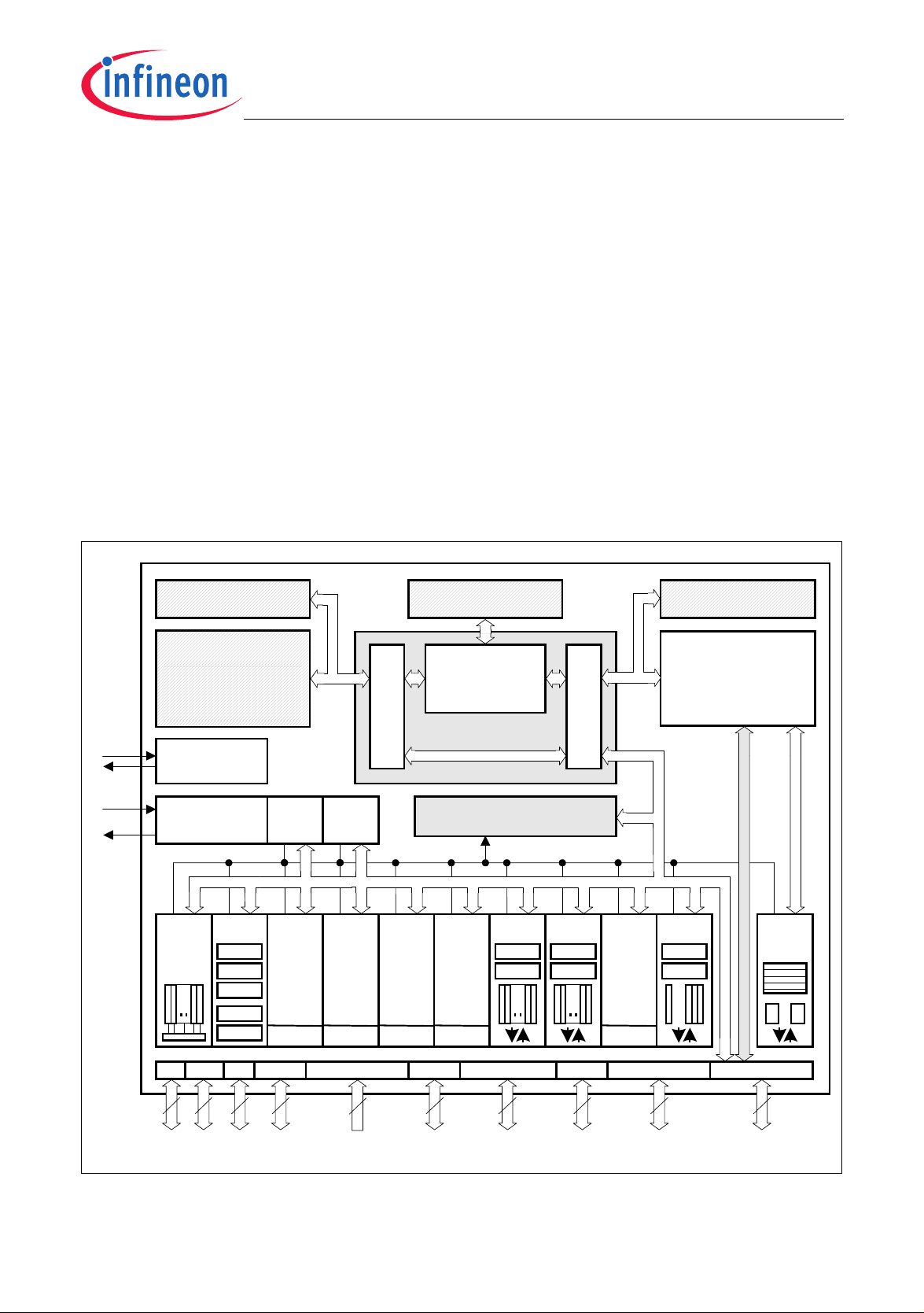
3 Functional Description
The architecture of the XC167 combines advantages of RISC, CISC, and DSP
processors with an advanced peripheral subsystem in a very well-balanced way. In
addition, the on-chip memory blocks allow the design of compact systems-on-silicon with
maximum performance (computing, control, communication).
The on-chip memory blocks (program code-memory and SRAM, dual-port RAM, data
SRAM) and the set of generic peripherals are connected to the CPU via separate buses.
Another bus, the LXBus, connects additional on-chip resources as well as external
resources (see Figure 3).
This bus structure enhances the overall system performance by enabling the concurrent
operation of several subsystems of the XC167.
The following block diagram gives an overview of the different on-chip components and
of the advanced, high bandwidth internal bus structure of the XC167.
XTAL
PSRAM DPRAM DSRAM
ProgMem
Flash
128 KBytes
PMU
CPU
DMU
C166SV2-Core
OCDS
Debug Support
Osc / PLL
Clock Generation
ADC
8/10-Bit
Channels
GPT
16
T2
T3
T4
T5
T6
RTC WDT
ASC0
(USAR T)
BRGen
ASC1
(USART)
BRGen
SSC0
(SPI)
BRGen
Interrupt & PEC
SSC1
(SPI)
BRGen
CC1
T0
T1
Interrupt Bus
Peripheral Data Bus
CC2
T7
T8
BRGen
IIC
CC6
EBC
XBUS Control
External Bus
Control
T12
T13
Twin
CAN
A B
P 20
4
66
Port 5
16
PORT1 PORT0Port 2Port 3Port 4Port 6P 7Port 9
81588
16
16
MCB04323_x7.vsd
Figure 3 Block Diagram
Data Sheet 21 V1.2, 2006-03

XC167-16
Derivatives
Functional Description
3.1 Memory Subsystem and Organization
The memory space of the XC167 is configured in a Von Neumann architecture, which
means that all internal and external resources, such as code memory, data memory,
registers and I/O ports, are organized within the same linear address space. This
common memory space includes 16 Mbytes and is arranged as 256 segments of
64 Kbytes each, where each segment consists of four data pages of 16 Kbytes each.
The entire memory space can be accessed bytewise or wordwise. Portions of the
on-chip DPRAM and the register spaces (E/SFR) have additionally been made directly
bitaddressable.
The internal data memory areas and the Special Function Register areas (SFR and
ESFR) are mapped into segment 0, the system segment.
The Program Management Unit (PMU) handles all code fetches and, therefore, controls
accesses to the program memories, such as Flash memory and PSRAM.
The Data Management Unit (DMU) handles all data transfers and, therefore, controls
accesses to the DSRAM and the on-chip peripherals.
Both units (PMU and DMU) are connected via the high-speed system bus to exchange
data. This is required if operands are read from program memory, code or data is written
to the PSRAM, code is fetched from external memory, or data is read from or written to
external resources, including peripherals on the LXBus (such as TwinCAN). The system
bus allows concurrent two-way communication for maximum transfer performance.
128 Kbytes of on-chip Flash memory store code or constant data. The on-chip Flash
memory is organized as four 8-Kbyte sectors, one 32-Kbyte sector, and one 64-Kbyte
sector. Each sector can be separately write protected
1)
, erased and programmed (in
blocks of 128 Bytes). The complete Flash area can be read-protected. A password
sequence temporarily unlocks protected areas. The Flash module combines very fast
64-bit one-cycle read accesses with protected and efficient writing algorithms for
programming and erasing. Thus, program execution out of the internal Flash results in
maximum performance. Dynamic error correction provides extremely high read data
security for all read accesses.
For timing characteristics, please refer to Section 4.4.2.
2 Kbytes of on-chip Program SRAM (PSRAM) are provided to store user code or data.
The PSRAM is accessed via the PMU and is therefore optimized for code fetches.
4 Kbytes of on-chip Data SRAM (DSRAM) are provided as a storage for general user
data. The DSRAM is accessed via the DMU and is therefore optimized for data
accesses.
2 Kbytes of on-chip Dual-Port RAM (DPRAM) are provided as a storage for user
defined variables, for the system stack, and general purpose register banks. A register
bank can consist of up to 16 wordwide (R0 to R15) and/or bytewide (RL0, RH0, …, RL7,
1) Each two 8-Kbyte sectors are combined for write-protection purposes.
Data Sheet 22 V1.2, 2006-03
XC167-16
Derivatives
Functional Description
RH7) so-called General Purpose Registers (GPRs).
The upper 256 bytes of the DPRAM are directly bitaddressable. When used by a GPR,
any location in the DPRAM is bitaddressable.
1024 bytes (2 × 512 bytes) of the address space are reserved for the Special Function
Register areas (SFR space and ESFR space). SFRs are wordwide registers which are
used for controlling and monitoring functions of the different on-chip units. Unused SFR
addresses are reserved for future members of the XC166 Family. Therefore, they should
either not be accessed, or written with zeros, to ensure upward compatibility.
In order to meet the needs of designs where more memory is required than is provided
on chip, up to 12 Mbytes (approximately, see Table 3) of external RAM and/or ROM can
be connected to the microcontroller. The External Bus Interface also provides access to
external peripherals.
Table 3 XC167 Memory Map
1)
Address Area Start Loc. End Loc. Area Size
Flash register space FF’F000
Reserved (Access trap) F8’0000
Reserved for PSRAM E0’0800
Program SRAM E0’0000
Reserved for pr. mem. C2’0000
Program Flash C0’0000
Reserved BF’0000
External memory area 40’0000
External IO area
4)
20’0800
TwinCAN registers 20’0000
External memory area 01’0000
H
H
H
H
H
H
H
H
H
H
H
FF’FFFF
FF’EFFF
F7’FFFF
E0’07FF
DF’FFFF
C1’FFFF
BF’FFFF
BE’FFFF
3F’FFFF
20’07FF
1F’FFFF
4 Kbytes
H
< 0.5 Mbytes Minus Flash
H
< 1.5 Mbytes Minus PSRAM
H
2 Kbytes Maximum
H
< 2 Mbytes Minus Flash
H
128 Kbytes –
H
64 Kbytes –
H
< 8 Mbytes Minus reserved
H
< 2 Mbytes Minus TwinCAN
H
2 Kbytes –
H
< 2 Mbytes Minus segment 0
H
2)
Notes
3)
registers
segment
Data RAMs and SFRs 00’8000
External memory area 00’0000
1) Accesses to the shaded areas generate external bus accesses.
2) The areas marked with “<” are slightly smaller than indicated, see column “Notes”.
3) Not defined register locations return a trap code.
4) Several pipeline optimizations are not active within the external IO area. This is necessary to control external
peripherals properly.
Data Sheet 23 V1.2, 2006-03
H
H
00’FFFF
00’7FFF
32 Kbytes Partly used
H
32 Kbytes –
H

XC167-16
Derivatives
Functional Description
3.2 External Bus Controller
All of the external memory accesses are performed by a particular on-chip External Bus
Controller (EBC). It can be programmed either to Single Chip Mode when no external
memory is required, or to one of four different external memory access modes
are as follows:
• 16 … 24-bit Addresses, 16-bit Data, Demultiplexed
• 16 … 24-bit Addresses, 16-bit Data, Multiplexed
• 16 … 24-bit Addresses, 8-bit Data, Multiplexed
• 16 … 24-bit Addresses, 8-bit Data, Demultiplexed
In the demultiplexed bus modes, addresses are output on PORT1 and data is
input/output on PORT0 or P0L, respectively. In the multiplexed bus modes both
addresses and data use PORT0 for input/output. The high order address (segment) lines
use Port 4. The number of active segment address lines is selectable, restricting the
external address space to 8 Mbytes … 64 Kbytes. This is required when interface lines
are assigned to Port 4.
1)
, which
Up to 5 external CS
signals (4 windows plus default) can be generated in order to save
external glue logic. External modules can directly be connected to the common
address/data bus and their individual select lines.
Access to very slow memories or modules with varying access times is supported via a
particular ‘Ready’ function. The active level of the control input signal is selectable.
A HOLD
/HLDA protocol is available for bus arbitration and allows the sharing of external
resources with other bus masters. The bus arbitration is enabled by software. After
enabling, pins P6.7 … P6.5 (BREQ
EBC. In Master Mode (default after reset) the HLDA
HLDA
is switched to input. This allows the direct connection of the slave controller to
, HLDA, HOLD) are automatically controlled by the
pin is an output. In Slave Mode pin
another master controller without glue logic.
Important timing characteristics of the external bus interface have been made
programmable (via registers TCONCSx/FCONCSx) to allow the user the adaption of a
wide range of different types of memories and external peripherals.
In addition, up to 4 independent address windows may be defined (via registers
ADDRSELx) which control the access to different resources with different bus
characteristics. These address windows are arranged hierarchically where window 4
overrides window 3, and window 2 overrides window 1. All accesses to locations not
covered by these 4 address windows are controlled by TCONCS0/FCONCS0. The
currently active window can generate a chip select signal.
The external bus timing is related to the rising edge of the reference clock output
CLKOUT. The external bus protocol is compatible with that of the standard C166 Family.
1) Bus modes are switched dynamically if several address windows with different mode settings are used.
Data Sheet 24 V1.2, 2006-03

XC167-16
Derivatives
Functional Description
The EBC also controls accesses to resources connected to the on-chip LXBus. The
LXBus is an internal representation of the external bus and allows accessing integrated
peripherals and modules in the same way as external components.
The TwinCAN module is connected and accessed via the LXBus.
Data Sheet 25 V1.2, 2006-03
XC167-16
Derivatives
Functional Description
3.3 Central Processing Unit (CPU)
The main core of the CPU consists of a 5-stage execution pipeline with a 2-stage
instruction-fetch pipeline, a 16-bit arithmetic and logic unit (ALU), a 32-bit/40-bit multiply
and accumulate unit (MAC), a register-file providing three register banks, and dedicated
SFRs. The ALU features a multiply and divide unit, a bit-mask generator, and a barrel
shifter.
CPU
Prefetch
Branch
Multiply
Unit
Unit
FIFO
IDX0
IDX1
QX0
QX1
+/-
Unit
+/-
CSP IP
CPUCON1
CPUCON2
Return
Stack
QR0
QR1
+/-
MRW
MCW
MSW
IFU
DPP0
DPP1
DPP2
DPP3
Division Unit
M ultip ly U n it
MDC
PSW
VECSEG
TFR
Injection/
Exception
Handler
SPSEG
SP
STKOV
STKUN
Bit-Mask-Gen.
Barrel-Shifter
+/-
ADU
PMU
2-Stage
5-Stage
R15
R14
GPRs
GPRs
RF
Prefetch
Pipeline
Pipeline
CP
R15
R15
R14
R14
GPRs
R1
R1
R0
R1
R0
R0
PSRAM
Flash/ROM
DPRAM
IPIP
R15
R14
GPRs
R1
R0
MAC
MAH
MAL
MDH
ZEROS
MDL
ONES
ALU
Buffer
DMU
WB
DSRAM
EBC
Peripherals
mca04917_x.vsd
Figure 4 CPU Block Diagram
Based on these hardware provisions, most of the XC167’s instructions can be executed
in just one machine cycle which requires 25 ns at 40 MHz CPU clock. For example, shift
Data Sheet 26 V1.2, 2006-03

XC167-16
Derivatives
Functional Description
and rotate instructions are always processed during one machine cycle independent of
the number of bits to be shifted. Also multiplication and most MAC instructions execute
in one single cycle. All multiple-cycle instructions have been optimized so that they can
be executed very fast as well: for example, a division algorithm is performed in 18 to 21
CPU cycles, depending on the data and division type. Four cycles are always visible, the
rest runs in the background. Another pipeline optimization, the branch target prediction,
allows eliminating the execution time of branch instructions if the prediction was correct.
The CPU has a register context consisting of up to three register banks with 16 wordwide
GPRs each at its disposal. The global register bank is physically allocated within the onchip DPRAM area. A Context Pointer (CP) register determines the base address of the
active global register bank to be accessed by the CPU at any time. The number of
register banks is only restricted by the available internal RAM space. For easy parameter
passing, a register bank may overlap others.
A system stack of up to 32 Kwords is provided as a storage for temporary data. The
system stack can be allocated to any location within the address space (preferably in the
on-chip RAM area), and it is accessed by the CPU via the stack pointer (SP) register.
Two separate SFRs, STKOV and STKUN, are implicitly compared against the stack
pointer value upon each stack access for the detection of a stack overflow or underflow.
The high performance offered by the hardware implementation of the CPU can efficiently
be utilized by a programmer via the highly efficient XC167 instruction set which includes
the following instruction classes:
• Standard Arithmetic Instructions
• DSP-Oriented Arithmetic Instructions
• Logical Instructions
• Boolean Bit Manipulation Instructions
• Compare and Loop Control Instructions
• Shift and Rotate Instructions
• Prioritize Instruction
• Data Movement Instructions
• System Stack Instructions
• Jump and Call Instructions
• Return Instructions
• System Control Instructions
• Miscellaneous Instructions
The basic instruction length is either 2 or 4 bytes. Possible operand types are bits, bytes
and words. A variety of direct, indirect or immediate addressing modes are provided to
specify the required operands.
Data Sheet 27 V1.2, 2006-03

XC167-16
Derivatives
Functional Description
3.4 Interrupt System
With an interrupt response time of typically 8 CPU clocks (in case of internal program
execution), the XC167 is capable of reacting very fast to the occurrence of nondeterministic events.
The architecture of the XC167 supports several mechanisms for fast and flexible
response to service requests that can be generated from various sources internal or
external to the microcontroller. Any of these interrupt requests can be programmed to
being serviced by the Interrupt Controller or by the Peripheral Event Controller (PEC).
In contrast to a standard interrupt service where the current program execution is
suspended and a branch to the interrupt vector table is performed, just one cycle is
‘stolen’ from the current CPU activity to perform a PEC service. A PEC service implies a
single byte or word data transfer between any two memory locations with an additional
increment of either the PEC source, or the destination pointer, or both. An individual PEC
transfer counter is implicitly decremented for each PEC service except when performing
in the continuous transfer mode. When this counter reaches zero, a standard interrupt is
performed to the corresponding source related vector location. PEC services are very
well suited, for example, for supporting the transmission or reception of blocks of data.
The XC167 has 8 PEC channels each of which offers such fast interrupt-driven data
transfer capabilities.
A separate control register which contains an interrupt request flag, an interrupt enable
flag and an interrupt priority bitfield exists for each of the possible interrupt nodes. Via its
related register, each node can be programmed to one of sixteen interrupt priority levels.
Once having been accepted by the CPU, an interrupt service can only be interrupted by
a higher prioritized service request. For the standard interrupt processing, each of the
possible interrupt nodes has a dedicated vector location.
Fast external interrupt inputs are provided to service external interrupts with high
precision requirements. These fast interrupt inputs feature programmable edge
detection (rising edge, falling edge, or both edges).
Software interrupts are supported by means of the ‘TRAP’ instruction in combination with
an individual trap (interrupt) number.
Table 4 shows all of the possible XC167 interrupt sources and the corresponding
hardware-related interrupt flags, vectors, vector locations and trap (interrupt) numbers.
Note: Interrupt nodes which are not assigned to peripherals (unassigned nodes), may
be used to generate software controlled interrupt requests by setting the
respective interrupt request bit (xIR).
Data Sheet 28 V1.2, 2006-03

Table 4 XC167 Interrupt Nodes
XC167-16
Derivatives
Functional Description
Source of Interrupt or PEC
Service Request
Control
Register
Vector
Location
CAPCOM Register 0 CC1_CC0IC xx’0040
CAPCOM Register 1 CC1_CC1IC xx’0044
CAPCOM Register 2 CC1_CC2IC xx’0048
CAPCOM Register 3 CC1_CC3IC xx’004C
CAPCOM Register 4 CC1_CC4IC xx’0050
CAPCOM Register 5 CC1_CC5IC xx’0054
CAPCOM Register 6 CC1_CC6IC xx’0058
CAPCOM Register 7 CC1_CC7IC xx’005C
CAPCOM Register 8 CC1_CC8IC xx’0060
CAPCOM Register 9 CC1_CC9IC xx’0064
CAPCOM Register 10 CC1_CC10IC xx’0068
CAPCOM Register 11 CC1_CC11IC xx’006C
CAPCOM Register 12 CC1_CC12IC xx’0070
Trap
1)
H
H
H
H
H
H
H
H
H
H
H
H
H
Number
10H / 16
11H / 17
12H / 18
13H / 19
14H / 20
15H / 21
16H / 22
17H / 23
18H / 24
19H / 25
1AH / 26
1BH / 27
1CH / 28
D
D
D
D
D
D
D
D
D
D
D
D
D
CAPCOM Register 13 CC1_CC13IC xx’0074
CAPCOM Register 14 CC1_CC14IC xx’0078
CAPCOM Register 15 CC1_CC15IC xx’007C
CAPCOM Register 16 CC2_CC16IC xx’00C0
CAPCOM Register 17 CC2_CC17IC xx’00C4
CAPCOM Register 18 CC2_CC18IC xx’00C8
CAPCOM Register 19 CC2_CC19IC xx’00CC
CAPCOM Register 20 CC2_CC20IC xx’00D0
CAPCOM Register 21 CC2_CC21IC xx’00D4
CAPCOM Register 22 CC2_CC22IC xx’00D8
CAPCOM Register 23 CC2_CC23IC xx’00DC
CAPCOM Register 24 CC2_CC24IC xx’00E0
CAPCOM Register 25 CC2_CC25IC xx’00E4
CAPCOM Register 26 CC2_CC26IC xx’00E8
CAPCOM Register 27 CC2_CC27IC xx’00EC
H
H
H
H
H
H
H
H
H
H
H
H
H
H
H
1DH / 29
1EH / 30
1FH / 31
30H / 48
31H / 49
32H / 50
33H / 51
34H / 52
35H / 53
36H / 54
37H / 55
38H / 56
39H / 57
3AH / 58
3BH / 59
D
D
D
D
D
D
D
D
D
D
D
D
D
D
D
CAPCOM Register 28 CC2_CC28IC xx’00F0
H
3CH / 60
D
Data Sheet 29 V1.2, 2006-03

Table 4 XC167 Interrupt Nodes (cont’d)
XC167-16
Derivatives
Functional Description
Source of Interrupt or PEC
Service Request
Control
Register
Vector
Location
CAPCOM Register 29 CC2_CC29IC xx’0110
CAPCOM Register 30 CC2_CC30IC xx’0114
CAPCOM Register 31 CC2_CC31IC xx’0118
CAPCOM Timer 0 CC1_T0IC xx’0080
CAPCOM Timer 1 CC1_T1IC xx’0084
CAPCOM Timer 7 CC2_T7IC xx’00F4
CAPCOM Timer 8 CC2_T8IC xx’00F8
GPT1 Timer 2 GPT12E_T2IC xx’0088
GPT1 Timer 3 GPT12E_T3IC xx’008C
GPT1 Timer 4 GPT12E_T4IC xx’0090
GPT2 Timer 5 GPT12E_T5IC xx’0094
GPT2 Timer 6 GPT12E_T6IC xx’0098
GPT2 CAPREL Register GPT12E_CRIC xx’009C
Trap
1)
H
H
H
H
H
H
H
H
H
H
H
H
H
Number
44H / 68
45H / 69
46H / 70
20H / 32
21H / 33
3DH / 61
3EH / 62
22H / 34
23H / 35
24H / 36
25H / 37
26H / 38
27H / 39
D
D
D
D
D
D
D
D
D
D
D
D
D
A/D Conversion Complete ADC_CIC xx’00A0
A/D Overrun Error ADC_EIC xx’00A4
ASC0 Transmit ASC0_TIC xx’00A8
ASC0 Transmit Buffer ASC0_TBIC xx’011C
ASC0 Receive ASC0_RIC xx’00AC
ASC0 Error ASC0_EIC xx’00B0
ASC0 Autobaud ASC0_ABIC xx’017C
SSC0 Transmit SSC0_TIC xx’00B4
SSC0 Receive SSC0_RIC xx’00B8
SSC0 Error SSC0_EIC xx’00BC
IIC Data Transfer Event IIC_DTIC xx’0100
IIC Protocol Event IIC_PEIC xx’0104
PLL/OWD PLLIC xx’010C
ASC1 Transmit ASC1_TIC xx’0120
ASC1 Transmit Buffer ASC1_TBIC xx’0178
H
H
H
H
H
H
H
H
H
H
H
H
H
H
H
28H / 40
29H / 41
2AH / 42
47H / 71
2BH / 43
2CH / 44
5FH / 95
2DH / 45
2EH / 46
2FH / 47
40H / 64
41H / 65
43H / 67
48H / 72
5EH / 94
D
D
D
D
D
D
D
D
D
D
D
D
D
D
D
ASC1 Receive ASC1_RIC xx’0124
ASC1 Error ASC1_EIC xx’0128
H
H
49H / 73
4AH / 74
D
D
Data Sheet 30 V1.2, 2006-03

Table 4 XC167 Interrupt Nodes (cont’d)
XC167-16
Derivatives
Functional Description
Source of Interrupt or PEC
Service Request
Control
Register
Vector
Location
ASC1 Autobaud ASC1_ABIC xx’0108
End of PEC Subchannel EOPIC xx’0130
CAPCOM6 Timer T12 CCU6_T12IC xx’0134
CAPCOM6 Timer T13 CCU6_T13IC xx’0138
CAPCOM6 Emergency CCU6_EIC xx’013C
CAPCOM6 CCU6_IC xx’0140
SSC1 Transmit SSC1_TIC xx’0144
SSC1 Receive SSC1_RIC xx’0148
SSC1 Error SSC1_EIC xx’014C
CAN0 CAN_0IC xx’0150
CAN1 CAN_1IC xx’0154
CAN2 CAN_2IC xx’0158
CAN3 CAN_3IC xx’015C
Trap
1)
H
H
H
H
H
H
H
H
H
H
H
H
H
Number
42H / 66
4CH / 76
4DH / 77
4EH / 78
4FH / 79
50H / 80
51H / 81
52H / 82
53H / 83
54H / 84
55H / 85
56H / 86
57H / 87
D
D
D
D
D
D
D
D
D
D
D
D
D
CAN4 CAN_4IC xx’0164
CAN5 CAN_5IC xx’0168
CAN6 CAN_6IC xx’016C
CAN7 CAN_7IC xx’0170
RTC RTC_IC xx’0174
Unassigned node – xx’012C
Unassigned node – xx’00FC
Unassigned node – xx’0160
1) Register VECSEG defines the segment where the vector table is located to.
Bitfield VECSC in register CPUCON1 defines the distance between two adjacent vectors. This table
represents the default setting, with a distance of 4 (two words) between two vectors.
H
H
H
H
H
H
H
H
59H / 89
5AH / 90
5BH / 91
5CH / 92
5DH / 93
4BH / 75
3FH / 63
58H / 88
D
D
D
D
D
D
D
D
Data Sheet 31 V1.2, 2006-03

XC167-16
Derivatives
Functional Description
The XC167 also provides an excellent mechanism to identify and to process exceptions
or error conditions that arise during run-time, so-called ‘Hardware Traps’. Hardware
traps cause immediate non-maskable system reaction which is similar to a standard
interrupt service (branching to a dedicated vector table location). The occurrence of a
hardware trap is additionally signified by an individual bit in the trap flag register (TFR).
Except when another higher prioritized trap service is in progress, a hardware trap will
interrupt any actual program execution. In turn, hardware trap services can normally not
be interrupted by standard or PEC interrupts.
Table 5 shows all of the possible exceptions or error conditions that can arise during run-
time:
Table 5 Hardware Trap Summary
Exception Condition Trap
Flag
Reset Functions:
–
• Hardware Reset
• Software Reset
• Watchdog Timer
Overflow
Class A Hardware Traps:
• Non-Maskable Interrupt
• Stack Overflow
• Stack Underflow
• Software Break
NMI
STKOF
STKUF
SOFTBRK
Class B Hardware Traps:
• Undefined Opcode
• PMI Access Error
• Protected Instruction
UNDOPC
PACER
PRTFLT
Fault
• Illegal Word Operand
ILLOPA
Access
Trap
Vector
RESET
RESET
RESET
NMITRAP
STOTRAP
STUTRAP
SBRKTRAP
BTRAP
BTRAP
BTRAP
BTRAP
Vector
Location
xx’0000
xx’0000
xx’0000
xx’0008
xx’0010
xx’0018
xx’0020
xx’0028
xx’0028
xx’0028
xx’0028
H
H
H
H
H
H
H
H
H
H
H
Trap
1)
Number
00
00
00
02
04
06
08
0A
0A
0A
0A
Trap
Priority
H
H
H
H
H
H
H
H
H
H
H
III
III
III
II
II
II
II
I
I
I
I
Reserved – – [2C
Software Traps
–– Any
• TRAP Instruction
- 3CH][0BH -
H
[xx’0000
xx’01FC
–
0F
]
H
Any
[00
-
H
]
H
7F
-
H
]
H
Current
CPU
Priority
in steps of
4
H
1) Register VECSEG defines the segment where the vector table is located to.
Data Sheet 32 V1.2, 2006-03

XC167-16
Derivatives
Functional Description
3.5 On-Chip Debug Support (OCDS)
The On-Chip Debug Support system provides a broad range of debug and emulation
features built into the XC167. The user software running on the XC167 can thus be
debugged within the target system environment.
The OCDS is controlled by an external debugging device via the debug interface,
consisting of the IEEE-1149-conforming JTAG port and a break interface. The debugger
controls the OCDS via a set of dedicated registers accessible via the JTAG interface.
Additionally, the OCDS system can be controlled by the CPU, e.g. by a monitor program.
An injection interface allows the execution of OCDS-generated instructions by the CPU.
Multiple breakpoints can be triggered by on-chip hardware, by software, or by an
external trigger input. Single stepping is supported as well as the injection of arbitrary
instructions and read/write access to the complete internal address space. A breakpoint
trigger can be answered with a CPU-halt, a monitor call, a data transfer, or/and the
activation of an external signal.
Tracing data can be obtained via the JTAG interface or via the external bus interface for
increased performance.
The debug interface uses a set of 6 interface signals (4 JTAG lines, 2 break lines) to
communicate with external circuitry. These interface signals use dedicated pins.
Complete system emulation is supported by the New Emulation Technology (NET)
interface.
Data Sheet 33 V1.2, 2006-03

XC167-16
Derivatives
Functional Description
3.6 Capture/Compare Units (CAPCOM1/2)
The CAPCOM units support generation and control of timing sequences on up to
32 channels with a maximum resolution of 1 system clock cycle (8 cycles in staggered
mode). The CAPCOM units are typically used to handle high speed I/O tasks such as
pulse and waveform generation, pulse width modulation (PMW), Digital to Analog (D/A)
conversion, software timing, or time recording relative to external events.
Four 16-bit timers (T0/T1, T7/T8) with reload registers provide two independent time
bases for each capture/compare register array.
The input clock for the timers is programmable to several prescaled values of the internal
system clock, or may be derived from an overflow/underflow of timer T6 in module GPT2.
This provides a wide range of variation for the timer period and resolution and allows
precise adjustments to the application specific requirements. In addition, external count
inputs for CAPCOM timers T0 and T7 allow event scheduling for the capture/compare
registers relative to external events.
Both of the two capture/compare register arrays contain 16 dual purpose
capture/compare registers, each of which may be individually allocated to either
CAPCOM timer T0 or T1 (T7 or T8, respectively), and programmed for capture or
compare function.
All registers of each module have each one port pin associated with it which serves as
an input pin for triggering the capture function, or as an output pin to indicate the
occurrence of a compare event.
Table 6 Compare Modes (CAPCOM1/2)
Compare Modes Function
Mode 0 Interrupt-only compare mode;
several compare interrupts per timer period are possible
Mode 1 Pin toggles on each compare match;
several compare events per timer period are possible
Mode 2 Interrupt-only compare mode;
only one compare interrupt per timer period is generated
Mode 3 Pin set ‘1’ on match; pin reset ‘0’ on compare timer overflow;
only one compare event per timer period is generated
Double Register
Mode
Single Event Mode Generates single edges or pulses;
Data Sheet 34 V1.2, 2006-03
Two registers operate on one pin;
pin toggles on each compare match;
several compare events per timer period are possible
can be used with any compare mode

XC167-16
Derivatives
Functional Description
When a capture/compare register has been selected for capture mode, the current
contents of the allocated timer will be latched (‘captured’) into the capture/compare
register in response to an external event at the port pin which is associated with this
register. In addition, a specific interrupt request for this capture/compare register is
generated. Either a positive, a negative, or both a positive and a negative external signal
transition at the pin can be selected as the triggering event.
The contents of all registers which have been selected for one of the five compare modes
are continuously compared with the contents of the allocated timers.
When a match occurs between the timer value and the value in a capture/compare
register, specific actions will be taken based on the selected compare mode.
Data Sheet 35 V1.2, 2006-03

f
f
Reload Reg.
T0REL/T7REL
XC167-16
Derivatives
Functional Description
CC
T0IN/T7IN
T6OUF
CCxIO
CCxIO
T0/T7
Input
Control
Mode
Control
(Capture
or
Compare)
Timer T0/T7
Sixteen
16-bit
Capture/
Compare
Registers
T0IRQ,
T7IRQ
CCxIRQ
CCxIRQ
CCxIO
CC
T6OUF
T1/T8
Input
Control
Timer T1/T8
CCxIRQ
T1IRQ,
T8IRQ
Reload Reg.
T1REL/T8REL
CAPCOM1 provides channels x = 0 … 15,
CAPCOM2 provides channels x = 16 … 31.
(see signals CCxIO and CCxIRQ)
MCB05569
Figure 5 CAPCOM1/2 Unit Block Diagram
Data Sheet 36 V1.2, 2006-03

XC167-16
Derivatives
Functional Description
3.7 The Capture/Compare Unit CAPCOM6
The CAPCOM6 unit supports generation and control of timing sequences on up to three
16-bit capture/compare channels plus one independent 10-bit compare channel.
In compare mode the CAPCOM6 unit provides two output signals per channel which
have inverted polarity and non-overlapping pulse transitions (deadtime control). The
compare channel can generate a single PWM output signal and is further used to
modulate the capture/compare output signals.
In capture mode the contents of compare timer T12 is stored in the capture registers
upon a signal transition at pins CCx.
Compare timers T12 (16-bit) and T13 (10-bit) are free running timers which are clocked
by the prescaled system clock.
f
f
CPU
CPU
Period Register
T12P
Offset Register
T12OF
Compare
Timer T12
Prescaler
Prescaler
16-bit
Control Register
CTCON
Compare
Timer T13
10-bit
Period Register
T13P
Mode
Select Register
CC6MSEL
CC Channel 0
CC60
CC Channel 1
Control
CC61
CC Channel 2
CC62
Compare Register
CMP13
Trap Register
Port
Control
Logic
Block
Commutation
Control
CC6MCON.H
CTRAP
CC60
COUT60
CC61
COUT61
CC62
COUT62
COUT63
CC6POS0
CC6POS1
CC6POS2
The timer registers (T12, T13) are not directly accessible.
The period and offset registers are loading a value into the timer registers.
MCB04109
Figure 6 CAPCOM6 Block Diagram
For motor control applications both subunits may generate versatile multichannel PWM
signals which are basically either controlled by compare timer T12 or by a typical hall
sensor pattern at the interrupt inputs (block commutation).
Data Sheet 37 V1.2, 2006-03

XC167-16
Derivatives
Functional Description
3.8 General Purpose Timer (GPT12E) Unit
The GPT12E unit represents a very flexible multifunctional timer/counter structure which
may be used for many different time related tasks such as event timing and counting,
pulse width and duty cycle measurements, pulse generation, or pulse multiplication.
The GPT12E unit incorporates five 16-bit timers which are organized in two separate
modules, GPT1 and GPT2. Each timer in each module may operate independently in a
number of different modes, or may be concatenated with another timer of the same
module.
Each of the three timers T2, T3, T4 of module GPT1 can be configured individually for
one of four basic modes of operation, which are Timer, Gated Timer, Counter, and
Incremental Interface Mode. In Timer Mode, the input clock for a timer is derived from
the system clock, divided by a programmable prescaler, while Counter Mode allows a
timer to be clocked in reference to external events.
Pulse width or duty cycle measurement is supported in Gated Timer Mode, where the
operation of a timer is controlled by the ‘gate’ level on an external input pin. For these
purposes, each timer has one associated port pin (TxIN) which serves as gate or clock
input. The maximum resolution of the timers in module GPT1 is 4 system clock cycles.
The count direction (up/down) for each timer is programmable by software or may
additionally be altered dynamically by an external signal on a port pin (TxEUD) to
facilitate e.g. position tracking.
In Incremental Interface Mode the GPT1 timers (T2, T3, T4) can be directly connected
to the incremental position sensor signals A and B via their respective inputs TxIN and
TxEUD. Direction and count signals are internally derived from these two input signals,
so the contents of the respective timer Tx corresponds to the sensor position. The third
position sensor signal TOP0 can be connected to an interrupt input.
Timer T3 has an output toggle latch (T3OTL) which changes its state on each timer
overflow/underflow. The state of this latch may be output on pin T3OUT e.g. for time out
monitoring of external hardware components. It may also be used internally to clock
timers T2 and T4 for measuring long time periods with high resolution.
In addition to their basic operating modes, timers T2 and T4 may be configured as reload
or capture registers for timer T3. When used as capture or reload registers, timers T2
and T4 are stopped. The contents of timer T3 is captured into T2 or T4 in response to a
signal at their associated input pins (TxIN). Timer T3 is reloaded with the contents of T2
or T4 triggered either by an external signal or by a selectable state transition of its toggle
latch T3OTL. When both T2 and T4 are configured to alternately reload T3 on opposite
state transitions of T3OTL with the low and high times of a PWM signal, this signal can
be constantly generated without software intervention.
Data Sheet 38 V1.2, 2006-03

f
T3CON.BPS1
XC167-16
Derivatives
Functional Description
GPT
2n:1
Basic Clock
Interrupt
T2IN
T2EUD
T2
Mode
Control
Aux. Timer T2
U/D
Reload
Request
(T2IRQ)
Capture
Interrupt
Request
(T3IRQ)
T3
T3IN
T3EUD
Mode
Control
Core Timer T3
U/D
T3OTL
Toggle
Latch
T3OUT
Capture
Reload
T4IN
T4EUD
T4
Mode
Control
Aux. Timer T4
U/D
Interrupt
Request
(T4IRQ)
MCA05563
Figure 7 Block Diagram of GPT1
With its maximum resolution of 2 system clock cycles, the GPT2 module provides
precise event control and time measurement. It includes two timers (T5, T6) and a
capture/reload register (CAPREL). Both timers can be clocked with an input clock which
is derived from the CPU clock via a programmable prescaler or with external signals. The
Data Sheet 39 V1.2, 2006-03

XC167-16
Derivatives
Functional Description
count direction (up/down) for each timer is programmable by software or may
additionally be altered dynamically by an external signal on a port pin (TxEUD).
Concatenation of the timers is supported via the output toggle latch (T6OTL) of timer T6,
which changes its state on each timer overflow/underflow.
The state of this latch may be used to clock timer T5, and/or it may be output on pin
T6OUT. The overflows/underflows of timer T6 can additionally be used to clock the
CAPCOM1/2 timers, and to cause a reload from the CAPREL register.
The CAPREL register may capture the contents of timer T5 based on an external signal
transition on the corresponding port pin (CAPIN), and timer T5 may optionally be cleared
after the capture procedure. This allows the XC167 to measure absolute time differences
or to perform pulse multiplication without software overhead.
The capture trigger (timer T5 to CAPREL) may also be generated upon transitions of
GPT1 timer T3’s inputs T3IN and/or T3EUD. This is especially advantageous when T3
operates in Incremental Interface Mode.
Data Sheet 40 V1.2, 2006-03

f
T6CON.BPS2
XC167-16
Derivatives
Functional Description
GPT
2n:1
Basic Clock
Interrupt
GPT2 Timer T5
Request
(T5IR)
T5
T5IN
Mode
Control
CAPIN
T3IN/
T3EUD
CAPREL
Mode
Control
U/D
Clear
Capture
Reload
Clear
GPT2 CAPREL
Interrupt
Request
(CRIR)
Interrupt
Request
(T6IR)
Toggle
FF
T6IN
T6
Mode
Control
GPT2 Timer T6 T6OTL
U/D
T6OUT
T6OUF
MCA05564
Figure 8 Block Diagram of GPT2
Data Sheet 41 V1.2, 2006-03

XC167-16
f
f
Derivatives
Functional Description
3.9 Real Time Clock
The Real Time Clock (RTC) module of the XC167 is directly clocked via a separate clock
driver either with the on-chip auxiliary oscillator frequency (
prescaled on-chip main oscillator frequency (
f
RTC
= f
/32). It is therefore independent
OSCm
from the selected clock generation mode of the XC167.
The RTC basically consists of a chain of divider blocks:
• a selectable 8:1 divider (on - off)
• the reloadable 16-bit timer T14
• the 32-bit RTC timer block (accessible via registers RTCH and RTCL), made of:
– a reloadable 10-bit timer
– a reloadable 6-bit timer
– a reloadable 6-bit timer
– a reloadable 10-bit timer
f
RTC
= f
) or with the
OSCa
All timers count up. Each timer can generate an interrupt request. All requests are
combined to a common node request.
RT C
:
8
MUX
RTCINT
Interrupt Sub Node
RUN
PRE
CNT
INT0
CNT
INT1
CNT
INT2
CNT
INT3
REL-Register
T14REL 10 Bits6 Bits6 Bits10 Bits
CNT
T14-Register
CNT-Register
10 Bits6 Bits6 Bits10 BitsT14
MCB05568
Figure 9 RTC Block Diagram
Note: The registers associated with the RTC are not affected by a reset in order to
maintain the correct system time even when intermediate resets are executed.
Data Sheet 42 V1.2, 2006-03

XC167-16
Derivatives
Functional Description
The RTC module can be used for different purposes:
• System clock to determine the current time and date,
optionally during idle mode, sleep mode, and power down mode
• Cyclic time based interrupt, to provide a system time tick independent of CPU
frequency and other resources, e.g. to wake up regularly from idle mode.
• 48-bit timer for long term measurements (maximum timespan is > 100 years).
• Alarm interrupt for wake-up on a defined time
Data Sheet 43 V1.2, 2006-03

XC167-16
Derivatives
Functional Description
3.10 A/D Converter
For analog signal measurement, a 10-bit A/D converter with 16 multiplexed input
channels and a sample and hold circuit has been integrated on-chip. It uses the method
of successive approximation. The sample time (for loading the capacitors) and the
conversion time is programmable (in two modes) and can thus be adjusted to the
external circuitry. The A/D converter can also operate in 8-bit conversion mode, where
the conversion time is further reduced.
Overrun error detection/protection is provided for the conversion result register
(ADDAT): either an interrupt request will be generated when the result of a previous
conversion has not been read from the result register at the time the next conversion is
complete, or the next conversion is suspended in such a case until the previous result
has been read.
For applications which require less analog input channels, the remaining channel inputs
can be used as digital input port pins.
The A/D converter of the XC167 supports four different conversion modes. In the
standard Single Channel conversion mode, the analog level on a specified channel is
sampled once and converted to a digital result. In the Single Channel Continuous mode,
the analog level on a specified channel is repeatedly sampled and converted without
software intervention. In the Auto Scan mode, the analog levels on a prespecified
number of channels are sequentially sampled and converted. In the Auto Scan
Continuous mode, the prespecified channels are repeatedly sampled and converted. In
addition, the conversion of a specific channel can be inserted (injected) into a running
sequence without disturbing this sequence. This is called Channel Injection Mode.
The Peripheral Event Controller (PEC) may be used to automatically store the
conversion results into a table in memory for later evaluation, without requiring the
overhead of entering and exiting interrupt routines for each data transfer.
After each reset and also during normal operation the ADC automatically performs
calibration cycles. This automatic self-calibration constantly adjusts the converter to
changing operating conditions (e.g. temperature) and compensates process variations.
These calibration cycles are part of the conversion cycle, so they do not affect the normal
operation of the A/D converter.
In order to decouple analog inputs from digital noise and to avoid input trigger noise
those pins used for analog input can be disconnected from the digital IO or input stages
under software control. This can be selected for each pin separately via register P5DIDIS
(Port 5 Digital Input Disable).
The Auto-Power-Down feature of the A/D converter minimizes the power consumption
when no conversion is in progress.
Data Sheet 44 V1.2, 2006-03

XC167-16
Derivatives
Functional Description
3.11 Asynchronous/Synchronous Serial Interfaces (ASC0/ASC1)
The Asynchronous/Synchronous Serial Interfaces ASC0/ASC1 (USARTs) provide serial
communication with other microcontrollers, processors, terminals or external peripheral
components. They are upward compatible with the serial ports of the Infineon 8-bit
microcontroller families and support full-duplex asynchronous communication and halfduplex synchronous communication. A dedicated baud rate generator with a fractional
divider precisely generates all standard baud rates without oscillator tuning. For
transmission, reception, error handling, and baudrate detection 5 separate interrupt
vectors are provided.
In asynchronous mode, 8- or 9-bit data frames (with optional parity bit) are transmitted
or received, preceded by a start bit and terminated by one or two stop bits. For
multiprocessor communication, a mechanism to distinguish address from data bytes has
been included (8-bit data plus wake-up bit mode). IrDA data transmissions up to
115.2 kbit/s with fixed or programmable IrDA pulse width are supported.
In synchronous mode, bytes (8 bits) are transmitted or received synchronously to a shift
clock which is generated by the ASC0/1. The LSB is always shifted first.
In both modes, transmission and reception of data is FIFO-buffered. An autobaud
detection unit allows to detect asynchronous data frames with its baudrate and mode
with automatic initialization of the baudrate generator and the mode control bits.
A number of optional hardware error detection capabilities has been included to increase
the reliability of data transfers. A parity bit can automatically be generated on
transmission or be checked on reception. Framing error detection allows to recognize
data frames with missing stop bits. An overrun error will be generated, if the last
character received has not been read out of the receive buffer register at the time the
reception of a new character is complete.
Summary of Features
• Full-duplex asynchronous operating modes
– 8- or 9-bit data frames, LSB first, one or two stop bits, parity generation/checking
– Baudrate from 2.5 Mbit/s to 0.6 bit/s (@ 40 MHz)
– Multiprocessor mode for automatic address/data byte detection
– Support for IrDA data transmission/reception up to max. 115.2 kbit/s (@ 40 MHz)
– Loop-back capability
– Auto baudrate detection
• Half-duplex 8-bit synchronous operating mode at 5 Mbit/s to 406.9 bit/s (@ 40 MHz)
• Buffered transmitter/receiver with FIFO support (8 entries per direction)
• Loop-back option available for testing purposes
• Interrupt generation on transmitter buffer empty condition, last bit transmitted
condition, receive buffer full condition, error condition (frame, parity, overrun error),
start and end of an autobaud detection
Data Sheet 45 V1.2, 2006-03

XC167-16
Derivatives
Functional Description
3.12 High Speed Synchronous Serial Channels (SSC0/SSC1)
The High Speed Synchronous Serial Channels SSC0/SSC1 support full-duplex and halfduplex synchronous communication. It may be configured so it interfaces with serially
linked peripheral components, full SPI functionality is supported.
A dedicated baud rate generator allows to set up all standard baud rates without
oscillator tuning. For transmission, reception and error handling three separate interrupt
vectors are provided.
The SSC transmits or receives characters of 2 … 16 bits length synchronously to a shift
clock which can be generated by the SSC (master mode) or by an external master (slave
mode). The SSC can start shifting with the LSB or with the MSB and allows the selection
of shifting and latching clock edges as well as the clock polarity.
A number of optional hardware error detection capabilities has been included to increase
the reliability of data transfers. Transmit error and receive error supervise the correct
handling of the data buffer. Phase error and baudrate error detect incorrect serial data.
Summary of Features
• Master or Slave mode operation
• Full-duplex or Half-duplex transfers
• Baudrate generation from 20 Mbit/s to 305.18 bit/s (@ 40 MHz)
• Flexible data format
– Programmable number of data bits: 2 to 16 bits
– Programmable shift direction: LSB-first or MSB-first
– Programmable clock polarity: idle low or idle high
– Programmable clock/data phase: data shift with leading or trailing clock edge
• Loop back option available for testing purposes
• Interrupt generation on transmitter buffer empty condition, receive buffer full
condition, error condition (receive, phase, baudrate, transmit error)
• Three pin interface with flexible SSC pin configuration
Data Sheet 46 V1.2, 2006-03

XC167-16
Derivatives
Functional Description
3.13 TwinCAN Module
The integrated TwinCAN module handles the completely autonomous transmission and
reception of CAN frames in accordance with the CAN specification V2.0 part B (active),
i.e. the on-chip TwinCAN module can receive and transmit standard frames with 11-bit
identifiers as well as extended frames with 29-bit identifiers.
Two Full-CAN nodes share the TwinCAN module’s resources to optimize the CAN bus
traffic handling and to minimize the CPU load. The module provides up to 32 message
objects, which can be assigned to one of the CAN nodes and can be combined to FIFOstructures. Each object provides separate masks for acceptance filtering.
The flexible combination of Full-CAN functionality and FIFO architecture reduces the
efforts to fulfill the real-time requirements of complex embedded control applications.
Improved CAN bus monitoring functionality as well as the number of message objects
permit precise and comfortable CAN bus traffic handling.
Gateway functionality allows automatic data exchange between two separate CAN bus
systems, which reduces CPU load and improves the real time behavior of the entire
system.
The bit timing for both CAN nodes is derived from the master clock and is programmable
up to a data rate of 1 Mbit/s. Each CAN node uses two pins of Port 4, Port 7, or Port 9 to
interface to an external bus transceiver. The interface pins are assigned via software.
TwinCAN Module Kernel
Clock
Control
Address
Decoder
f
CAN
CAN
Node A
Message
CAN
Node B
Object
Buffer
TxDCA
RxDCA
Port
Control
TxDCB
Interrupt
Control
TwinCAN Control
RxDCB
MCB05567
Figure 10 TwinCAN Module Block Diagram
Data Sheet 47 V1.2, 2006-03

XC167-16
Derivatives
Functional Description
Summary of Features
• CAN functionality according to CAN specification V2.0 B active
• Data transfer rate up to 1 Mbit/s
• Flexible and powerful message transfer control and error handling capabilities
• Full-CAN functionality and Basic CAN functionality for each message object
• 32 flexible message objects
– Assignment to one of the two CAN nodes
– Configuration as transmit object or receive object
– Concatenation to a 2-, 4-, 8-, 16-, or 32-message buffer with FIFO algorithm
– Handling of frames with 11-bit or 29-bit identifiers
– Individual programmable acceptance mask register for filtering for each object
– Monitoring via a frame counter
– Configuration for Remote Monitoring Mode
• Up to eight individually programmable interrupt nodes can be used
• CAN Analyzer Mode for bus monitoring is implemented
Note: When a CAN node has the interface lines assigned to Port 4, the segment address
output on Port 4 must be limited. CS
of addressable external memory.
lines can be used to increase the total amount
3.14 IIC Bus Module
The integrated IIC Bus Module handles the transmission and reception of frames over
the two-line IIC bus in accordance with the IIC Bus specification. The IIC Module can
operate in slave mode, in master mode or in multi-master mode. It can receive and
transmit data using 7-bit or 10-bit addressing. Up to 4 send/receive data bytes can be
stored in the extended buffers.
Several physical interfaces (port pins) can be established under software control. Data
can be transferred at speeds up to 400 kbit/s.
Two interrupt nodes dedicated to the IIC module allow efficient interrupt service and also
support operation via PEC transfers.
Note: The port pins associated with the IIC interfaces must be switched to open drain
mode, as required by the IIC specification.
Data Sheet 48 V1.2, 2006-03

XC167-16
Derivatives
Functional Description
3.15 Watchdog Timer
The Watchdog Timer represents one of the fail-safe mechanisms which have been
implemented to prevent the controller from malfunctioning for longer periods of time.
The Watchdog Timer is always enabled after a reset of the chip, and can be disabled
until the EINIT instruction has been executed (compatible mode), or it can be disabled
and enabled at any time by executing instructions DISWDT and ENWDT (enhanced
mode). Thus, the chip’s start-up procedure is always monitored. The software has to be
designed to restart the Watchdog Timer before it overflows. If, due to hardware or
software related failures, the software fails to do so, the Watchdog Timer overflows and
generates an internal hardware reset and pulls the RSTOUT
external hardware components to be reset.
The Watchdog Timer is a 16-bit timer, clocked with the system clock divided by
2/4/128/256. The high byte of the Watchdog Timer register can be set to a prespecified
reload value (stored in WDTREL) in order to allow further variation of the monitored time
interval. Each time it is serviced by the application software, the high byte of the
Watchdog Timer is reloaded and the low byte is cleared. Thus, time intervals between
13 µs and 419 ms can be monitored (@ 40 MHz).
The default Watchdog Timer interval after reset is 3.28 ms (@ 40 MHz).
pin low in order to allow
Data Sheet 49 V1.2, 2006-03

XC167-16
Derivatives
Functional Description
3.16 Clock Generation
The Clock Generation Unit uses a programmable on-chip PLL with multiple prescalers
to generate the clock signals for the XC167 with high flexibility. The master clock
the reference clock signal, and is used for TwinCAN and is output to the external system.
The CPU clock
directly (1:1) or via a 2:1 prescaler (
f
and the system clock f
CPU
f
SYS
= f
are derived from the master clock either
SYS
= fMC / 2). See also Section 4.4.1.
CPU
The on-chip oscillator can drive an external crystal or accepts an external clock signal.
The oscillator clock frequency can be multiplied by the on-chip PLL (by a programmable
factor) or can be divided by a programmable prescaler factor.
If the bypass mode is used (direct drive or prescaler) the PLL can deliver an independent
clock to monitor the clock signal generated by the on-chip oscillator. This PLL clock is
independent from the XTAL1 clock. When the expected oscillator clock transitions are
missing the Oscillator Watchdog (OWD) activates the PLL Unlock/OWD interrupt node
and supplies the CPU with an emergency clock, the PLL clock signal. Under these
circumstances the PLL will oscillate with its basic frequency.
f
MC
is
The oscillator watchdog can be disabled by switching the PLL off. This reduces power
consumption, but also no interrupt request will be generated in case of a missing
oscillator clock.
Note: At the end of an external reset (EA
via hardware by (externally) pulling the RD
= ‘0’) the oscillator watchdog may be disabled
line low upon a reset, similar to the
standard reset configuration.
3.17 Parallel Ports
The XC167 provides up to 103 I/O lines which are organized into nine input/output ports
and one input port. All port lines are bit-addressable, and all input/output lines are
individually (bit-wise) programmable as inputs or outputs via direction registers. The I/O
ports are true bidirectional ports which are switched to high impedance state when
configured as inputs. The output drivers of some I/O ports can be configured (pin by pin)
for push/pull operation or open-drain operation via control registers. During the internal
reset, all port pins are configured as inputs (except for pin RSTOUT
The edge characteristics (shape) and driver characteristics (output current) of the port
drivers can be selected via registers POCONx.
The input threshold of some ports is selectable (TTL or CMOS like), where the special
CMOS like input threshold reduces noise sensitivity due to the input hysteresis. The
input threshold may be selected individually for each byte of the respective ports.
).
All port lines have programmable alternate input or output functions associated with
them. All port lines that are not used for these alternate functions may be used as general
purpose IO lines.
Data Sheet 50 V1.2, 2006-03

Table 7 Summary of the XC167’s Parallel Ports
Port Control Alternate Functions
PORT0 Pad drivers Address/Data lines or data lines
PORT1 Pad drivers Address lines
2)
Capture inputs or compare outputs,
Serial interface lines
XC167-16
Derivatives
Functional Description
1)
Port 2 Pad drivers,
Open drain,
Input threshold
Port 3 Pad drivers,
Open drain,
Input threshold
Port 4 Pad drivers,
Open drain,
Capture inputs or compare outputs,
Timer control signal,
Fast external interrupt inputs
Timer control signals, serial interface lines,
Optional bus control signal BHE
/WRH,
System clock output CLKOUT (or FOUT)
Segment address lines
CAN interface lines
3)
4)
Input threshold
Port 5 – Analog input channels to the A/D converter,
Timer control signals
Port 6 Open drain,
Input threshold
Capture inputs or compare outputs,
Bus arbitration signals BREQ
, HLDA, HOLD,
Optional chip select signals
Port 7 Open drain,
Input threshold
Port 9 Pad drivers,
Open drain,
Input threshold
Capture inputs or compare outputs,
CAN interface lines
4)
Capture inputs or compare outputs
CAN interface lines
IIC bus interface lines
4)
,
4)
Port 20 Pad drivers,
Open drain
Bus control signals RD, WR/WRL, READY, ALE,
External access enable pin EA
,
Reset indication output RSTOUT
1) For multiplexed bus cycles.
2) For demultiplexed bus cycles.
3) For more than 64 Kbytes of external resources.
4) Can be assigned by software.
Data Sheet 51 V1.2, 2006-03

XC167-16
Derivatives
Functional Description
3.18 Power Management
The XC167 provides several means to control the power it consumes either at a given
time or averaged over a certain timespan. Three mechanisms can be used (partly in
parallel):
• Power Saving Modes switch the XC167 into a special operating mode (control via
instructions).
Idle Mode stops the CPU while the peripherals can continue to operate.
Sleep Mode and Power Down Mode stop all clock signals and all operation (RTC may
optionally continue running). Sleep Mode can be terminated by external interrupt
signals.
• Clock Generation Management controls the distribution and the frequency of
internal and external clock signals. While the clock signals for currently inactive parts
of logic are disabled automatically, the user can reduce the XC167’s CPU clock
frequency which drastically reduces the consumed power.
External circuitry can be controlled via the programmable frequency output FOUT.
• Peripheral Management permits temporary disabling of peripheral modules (control
via register SYSCON3). Each peripheral can separately be disabled/enabled.
The on-chip RTC supports intermittent operation of the XC167 by generating cyclic
wake-up signals. This offers full performance to quickly react on action requests while
the intermittent sleep phases greatly reduce the average power consumption of the
system.
Data Sheet 52 V1.2, 2006-03

XC167-16
Derivatives
Functional Description
3.19 Instruction Set Summary
Table 8 lists the instructions of the XC167 in a condensed way.
The various addressing modes that can be used with a specific instruction, the operation
of the instructions, parameters for conditional execution of instructions, and the opcodes
for each instruction can be found in the “Instruction Set Manual”.
This document also provides a detailed description of each instruction.
Table 8 Instruction Set Summary
Mnemonic Description Bytes
ADD(B) Add word (byte) operands 2 / 4
ADDC(B) Add word (byte) operands with Carry 2 / 4
SUB(B) Subtract word (byte) operands 2 / 4
SUBC(B) Subtract word (byte) operands with Carry 2 / 4
MUL(U) (Un)Signed multiply direct GPR by direct GPR
(16- × 16-bit)
DIV(U) (Un)Signed divide register MDL by direct GPR (16-/16-bit) 2
DIVL(U) (Un)Signed long divide reg. MD by direct GPR (32-/16-bit) 2
CPL(B) Complement direct word (byte) GPR 2
NEG(B) Negate direct word (byte) GPR 2
AND(B) Bitwise AND, (word/byte operands) 2 / 4
(X)OR(B) Bitwise (exclusive) OR, (word/byte operands) 2 / 4
BCLR/BSET Clear/Set direct bit 2
BMOV(N) Move (negated) direct bit to direct bit 4
BAND/BOR/BXOR AND/OR/XOR direct bit with direct bit 4
BCMP Compare direct bit to direct bit 4
BFLDH/BFLDL Bitwise modify masked high/low byte of bit-addressable
direct word memory with immediate data
2
4
CMP(B) Compare word (byte) operands 2 / 4
CMPD1/2 Compare word data to GPR and decrement GPR by 1/2 2 / 4
CMPI1/2 Compare word data to GPR and increment GPR by 1/2 2 / 4
PRIOR Determine number of shift cycles to normalize direct
word GPR and store result in direct word GPR
SHL/SHR Shift left/right direct word GPR 2
ROL/ROR Rotate left/right direct word GPR 2
Data Sheet 53 V1.2, 2006-03
2

XC167-16
Derivatives
Functional Description
Table 8 Instruction Set Summary (cont’d)
Mnemonic Description Bytes
ASHR Arithmetic (sign bit) shift right direct word GPR 2
MOV(B) Move word (byte) data 2 / 4
MOVBS/Z Move byte operand to word op. with sign/zero extension 2 / 4
JMPA/I/R Jump absolute/indirect/relative if condition is met 4
JMPS Jump absolute to a code segment 4
JB(C) Jump relative if direct bit is set (and clear bit) 4
JNB(S) Jump relative if direct bit is not set (and set bit) 4
CALLA/I/R Call absolute/indirect/relative subroutine if condition is met 4
CALLS Call absolute subroutine in any code segment 4
PCALL Push direct word register onto system stack and call
absolute subroutine
TRAP Call interrupt service routine via immediate trap number 2
PUSH/POP Push/pop direct word register onto/from system stack 2
SCXT Push direct word register onto system stack and update
register with word operand
RET(P) Return from intra-segment subroutine
(and pop direct word register from system stack)
RETS Return from inter-segment subroutine 2
RETI Return from interrupt service subroutine 2
SBRK Software Break 2
SRST Software Reset 4
IDLE Enter Idle Mode 4
PWRDN Enter Power Down Mode (supposes NMI
-pin being low) 4
SRVWDT Service Watchdog Timer 4
DISWDT/ENWDT Disable/Enable Watchdog Timer 4
4
4
2
EINIT Signify End-of-Initialization on RSTOUT
pin 4
ATOMIC Begin ATOMIC sequence 2
EXTR Begin EXTended Register sequence 2
EXTP(R) Begin EXTended Page (and Register) sequence 2 / 4
EXTS(R) Begin EXTended Segment (and Register) sequence 2 / 4
NOP Null operation 2
Data Sheet 54 V1.2, 2006-03

XC167-16
Derivatives
Functional Description
Table 8 Instruction Set Summary (cont’d)
Mnemonic Description Bytes
CoMUL/CoMAC Multiply (and accumulate) 4
CoADD/CoSUB Add/Subtract 4
Co(A)SHR/CoSHL (Arithmetic) Shift right/Shift left 4
CoLOAD/STORE Load accumulator/Store MAC register 4
CoCMP/MAX/MIN Compare (maximum/minimum) 4
CoABS/CoRND Absolute value/Round accumulator 4
CoMOV/NEG/NOP Data move/Negate accumulator/Null operation 4
Data Sheet 55 V1.2, 2006-03

Derivatives
Electrical Parameters
4 Electrical Parameters
4.1 General Parameters
Table 9 Absolute Maximum Ratings
Parameter Symbol Limit Values Unit Notes
Min. Max.
Storage temperature
T
ST
-65 150 °C
1)
XC167-16
Junction temperature T
Voltage on
respect to ground (
Voltage on
respect to ground (
V
pins with
DDI
V
DDP
V
)
SS
pins with
V
)
SS
Voltage on any pin with
respect to ground (
V
SS
)
Input current on any pin
J
V
DDI
V
DDP
V
IN
–-1010mA–
-40 150 °C under bias
-0.5 3.25 V –
-0.5 6.2 V –
-0.5 V
DDP
+
V–
0.5
during overload condition
Absolute sum of all input
– – |100| mA –
currents during overload
condition
1) Moisture Sensitivity Level (MSL) 3, conforming to Jedec J-STD-020C for 240 °C.
Note: Stresses above those listed under “Absolute Maximum Ratings” may cause
permanent damage to the device. This is a stress rating only and functional
operation of the device at these or any other conditions above those indicated in
the operational sections of this specification is not implied. Exposure to absolute
maximum rating conditions for extended periods may affect device reliability.
During absolute maximum rating overload conditions (
voltage on
V
pins with respect to ground (VSS) must not exceed the values
DDP
V
IN
> V
or VIN < VSS) the
DDP
defined by the absolute maximum ratings.
Data Sheet 56 V1.2, 2006-03

XC167-16
Derivatives
Electrical Parameters
Operating Conditions
The following operating conditions must not be exceeded to ensure correct operation of
the XC167. All parameters specified in the following sections refer to these operating
conditions, unless otherwise noticed.
Table 10 Operating Condition Parameters
Parameter Symbol Limit Values Unit Notes
Min. Max.
Digital supply voltage for
V
the core
Digital supply voltage for
V
IO pads
Supply Voltage Difference ∆
Digital ground voltage V
Overload current
Overload current coupling
factor for analog inputs
Overload current coupling
factor for digital I/O pins
Absolute sum of overload
I
K
6)
K
6)
Σ|
currents
External Load
C
Capacitance
DDI
DDP
V
SS
OV
DD
2.35 2.7 V Active mode,
4.4 5.5 V Active mode2)
-0.5 – V V
0 V Reference voltage
-5 5 mA Per IO pin
-2 5 mA Per analog input
OVA
OVD
I
OV
L
–1.0 × 10⁻⁴– IOV > 0
–1.5 × 10
-3
–5.0 × 10⁻³– IOV > 0
–1.0 × 10
-2
|– 50 mA
– 50 pF Pin drivers in
f
= f
CPU
- V
DDP
4)5)
pin
– IOV < 0
– IOV < 0
5)
default mode
CPUmax
1)2)
3)
DDI
4)5)
7)
Ambient temperature T
1) f
2) External circuitry must guarantee low level at the RSTIN
3) This limitation must be fulfilled under all operating conditions including power-ramp-up, power-ramp-down,
4) Overload conditions occur if the standard operating conditions are exceeded, i.e. the voltage on any pin
5) Not subject to production test - verified by design/characterization.
= 40 MHz for devices marked … 40F, f
CPUmax
reached their operating range.
and power-save modes.
exceeds the specified range:
input overload currents on all pins may not exceed 50 mA. The supply voltages must remain within the
specified limits.
Proper operation is not guaranteed if overload conditions occur on functional pins such as XTAL1, RD
etc.
A
V
> V
OV
DDP
––°C see Table 1
= 20 MHz for devices marked … 20F.
CPUmax
pin at least until both power supply voltages have
+ 0.5 V (IOV > 0) or VOV < VSS - 0.5 V (IOV < 0). The absolute sum of
, WR,
Data Sheet 57 V1.2, 2006-03

XC167-16
Derivatives
Electrical Parameters
6) An overload current (IOV) through a pin injects a certain error current (I
current adds to the respective pin’s leakage current (
current and is defined by the overload coupling factor
compared to the polarity of the overload current that produces it.
The total current through a pin is |
voltage on analog inputs.
7) The timing is valid for pin drivers operating in default current mode (selected after reset). Reducing the output
current may lead to increased delays or reduced driving capability (
I
| = |IOZ| + (|IOV| × KOV). The additional error current may distort the input
TOT
I
). The amount of error current depends on the overload
OZ
K
. The polarity of the injected error current is inverse
OV
) into the adjacent pins. This error
INJ
C
).
L
Parameter Interpretation
The parameters listed in the following partly represent the characteristics of the XC167
and partly its demands on the system. To aid in interpreting the parameters right, when
evaluating them for a design, they are marked in column “Symbol”:
CC (Controller Characteristics):
The logic of the XC167 will provide signals with the respective characteristics.
SR (System Requirement):
The external system must provide signals with the respective characteristics to the
XC167.
Data Sheet 58 V1.2, 2006-03

4.2 DC Parameters
XC167-16
Derivatives
Electrical Parameters
Table 11 DC Characteristics (Operating Conditions apply)
1)
Parameter Symbol Limit Values Unit Test Condition
Min. Max.
Input low voltage TTL
(all except XTAL1,
V
IL
SR -0.5 0.2 × V
V–
DDP
- 0.1
XTAL3)
Input low voltage for
XTAL1, XTAL3
2)
Input low voltage
(Special Threshold)
Input high voltage TTL
(all except XTAL1,
V
V
V
ILC
ILS
IH
SR -0.5 0.3 × V
SR -0.5 0.45 ×
V
DDP
SR 0.2 × V
DDP
V
+ 0.5 V –
DDP
+ 0.9
V–
DDI
V
3)
XTAL3)
Input high voltage
XTAL1, XTAL3
2)
Input high voltage
(Special Threshold)
V
V
IHC
IHS
SR 0.7 × V
SR 0.8 × V
- 0.2
DDI
DDP
V
+ 0.5 V –
DDI
V
+ 0.5 V
DDP
3)
Input Hysteresis
HYS 0.04 ×
(Special Threshold)
Output low voltage V
Output high voltage
Input leakage current
(Port 5)
7)
Input leakage current
(all other
8))7)
Configuration pull-up
current
9)
6)
V
I
I
I
I
OL
OH
OZ1
OZ2
CPUH
CPUL
V
–VV
DDP
in [V],
DDP
Series resistance = 0 Ω
CC – 1.0 V IOL ≤ I
–0.45VIOL ≤ I
CC V
- 1.0 – V IOH ≥ I
DDP
V
DDP
-
–VIOH ≥ I
0.45
CC – ±300 nA 0 V < VIN < V
T
≤ 125 °C
A
±200 nA 0 V <
T
≤ 85 °C
A
CC – ±500 nA 0.45 V < VIN <
V
DDP
10)
11)
–-10µA VIN = V
-100 – µA VIN = V
OLmax
OLnom
OHmax
OHnom
V
IN
IHmin
ILmax
< V
14)
3)
4)
4)5)
4)
4)5)
DDP
DDP
,
,
Data Sheet 59 V1.2, 2006-03

XC167-16
Derivatives
Electrical Parameters
Table 11 DC Characteristics (Operating Conditions apply)1) (cont’d)
Parameter Symbol Limit Values Unit Test Condition
Min. Max.
Configuration pulldown current
12)
Level inactive hold
current
13)
Level active hold
current
13)
I
CPDL
I
CPDH
I
LHI
I
LHA
10)
11)
10)
11)
–10µA VIN = V
120 – µA VIN = V
–-10µA V
-100 – µA V
V
OUT
DDP
OUT
= 0.5 ×
= 0.45 V
ILmax
IHmin
XTAL1, XTAL3 input
I
IL
CC – ±20 µA0 V < VIN < V
DDI
current
Pin capacitance
14)
C
IO
CC – 10 pF –
(digital inputs/outputs)
1) Keeping signal levels within the limits specified in this table, ensures operation without overload conditions.
For signal levels outside these specifications, also refer to the specification of the overload current
V
2) If XTAL3 is driven by a crystal, reaching an amplitude (peak to peak) of 0.25 ×
3) This parameter is tested for P2, P3, P4, P6, P7, P9.
4) The maximum deliverable output current of a port driver depends on the selected output driver mode, see
Table 12, Current Limits for Port Output Drivers. The limit for pin groups must be respected.
5) As a rule, with decreasing output current the output levels approach the respective supply level (
V
→ V
OH
6) This specification is not valid for outputs which are switched to open drain mode. In this case the respective
output will float and the voltage results from the external circuitry.
7) An additional error current (
the definition of the overload coupling factor
8) The driver of P3.15 is designed for faster switching, because this pin can deliver the reference clock for the
bus interface (CLKOUT). The maximum leakage current for P3.15 is, therefore, increased to 1 µA.
9) This specification is valid during Reset for configuration on RD
The pull-ups on RD
10) The maximum current may be drawn while the respective signal line remains inactive.
11) The minimum current must be drawn to drive the respective signal line active.
12) This specification is valid during Reset for configuration on ALE.
The pull-down on ALE is also active during bus hold.
13) This specification is valid during Reset for pins P6.4-0, which can act as CS
The pull-ups on CS
The pull-up on pin HLDA
14) Not subject to production test - verified by design/characterization.
). However, only the levels for nominal output currents are guaranteed.
DDP
I
) will flow if an overload current flows through an adjacent pin. Please refer to
INJ
K
.
OV
, WR, EA, PORT0.
and WR (WRL/WRH) are also active during bus hold.
outputs are also active during bus hold.
is active when arbitration is enabled and the EBC operates in slave mode.
outputs.
is sufficient.
DDI
I
OV
V
OL
.
→ VSS,
Data Sheet 60 V1.2, 2006-03

Table 12 Current Limits for Port Output Drivers
XC167-16
Derivatives
Electrical Parameters
Port Output Driver
Mode
Maximum Output Current
I
(
OLmax
, -I
OHmax
1)
)
Nominal Output Current
(
I
OLnom
, -I
OHnom
)
Strong driver 10 mA 2.5 mA
Medium driver 4.0 mA 1.0 mA
Weak driver 0.5 mA 0.1 mA
1) An output current above |I
For any group of 16 neighboring port output pins the total output current in each direction (Σ
remain below 50 mA.
| may be drawn from up to three pins at the same time.
OXnom
Table 13 Power Consumption XC167 (Operating Conditions apply)
Parameter Sym-
bol
Power supply current (active)
I
DDI
with all peripherals active
Pad supply current I
Idle mode supply current
DDP
I
IDX
with all peripherals active
Sleep and Power down mode
I
PDL
5)
supply current caused by
leakage
4)
Limit Values Unit Test Condition
Min. Max.
– 15 +
2.6 ×
f
CPU
–5 mA
– 15 +
1.2 ×
f
CPU
– 128,000
-α
× e
mA f
3)
mA f
mA V
T
in [MHz]
CPU
in [MHz]
CPU
DDI
in [°C]
J
α =
4670 / (273 +
Sleep and Power down mode
supply current caused by
leakage and the RTC running,
clocked by the main oscillator
4)
I
PDM
7)
– 0.6 +
0.02 ×
+
I
PDL
f
OSC
mA V
f
OSC
DDI
in [MHz]
I
and Σ-IOH) must
OL
= V
DDImax
= V
DDImax
1)2)
2)
6)
T
)
J
Sleep and Power down mode
I
PDA
– 0.1 + I
PDL
mA V
DDI
= V
DDImax
supply current caused by
leakage and the RTC running,
clocked by the auxiliary
or VIH.
4)
V
and maximum CPU clock frequency with all outputs disconnected and
DDImax
) mainly provides the current consumed by the pin output drivers. A small
DDP
V
supply.
DDP
oscillator at 32 kHz
1) During Flash programming or erase operations the supply current is increased by max. 5 mA.
2) The supply current is a function of the operating frequency. This dependency is illustrated in Figure 11.
These parameters are tested at
all inputs at
3) The pad supply voltage pins (V
amount of current is consumed even though no outputs are driven, because the drivers’ input stages are
switched and also the Flash module draws some power from the
Data Sheet 61 V1.2, 2006-03
V
IL

XC167-16
Derivatives
Electrical Parameters
4) The total supply current in Sleep and Power down mode is the sum of the temperature dependent leakage
current and the frequency dependent current for RTC and main oscillator or auxiliary oscillator (if active).
5) This parameter is determined mainly by the transistor leakage currents. This current heavily depends on the
junction temperature (see Figure 13). The junction temperature
if no current flows through the port output drivers. Otherwise, the resulting temperature difference must be
taken into account.
6) All inputs (including pins configured as inputs) at 0 V to 0.1 V or at
pins configured as outputs) disconnected. This parameter is tested at 25 °C and is valid for
7) This parameter is determined mainly by the current consumed by the oscillator switched to low gain mode (see
Figure 12). This current, however, is influenced by the external oscillator circuitry (crystal, capacitors). The
given values refer to a typical circuitry and may change in case of a not optimized external oscillator circuitry.
T
is the same as the ambient temperature T
J
V
- 0.1 V to V
DDP
, all outputs (including
DDP
T
≥ 25 °C.
J
A
Data Sheet 62 V1.2, 2006-03

I [mA]
140
XC167-16
Derivatives
Electrical Parameters
I
DDImax
120
100
80
60
40
I
DDItyp
I
IDXmax
I
IDXtyp
20
10 20 30 40
f
CPU
[MHz]
Figure 11 Supply/Idle Current as a Function of Operating Frequency
Data Sheet 63 V1.2, 2006-03

I [mA]
3.0
2.0
1.0
XC167-16
Derivatives
Electrical Parameters
I
PDMmax
I
PDMtyp
I
0.1
32 kHz
PDAmax
4 8 12 16
f
OSC
[MHz]
Figure 12 Sleep and Power Down Supply Current due to RTC and Oscillator
Running, as a Function of Oscillator Frequency
I
PDO
[mA]
1.5
1.0
0.5
-50
0 50 100 150
T
[°C]
J
Figure 13 Sleep and Power Down Leakage Supply Current as a Function of
Temperature
Data Sheet 64 V1.2, 2006-03

Derivatives
Electrical Parameters
4.3 Analog/Digital Converter Parameters
Table 14 A/D Converter Characteristics (Operating Conditions apply)
Parameter Symbol Limit Values Unit Test
Condition
1)
Analog reference supply
V
AREF
Min. Max.
SR 4.5 V
+ 0.1
DDP
V
XC167-16
Analog reference ground V
Analog input voltage range
Basic clock frequency f
Conversion time for 10-bit
result
4)
Conversion time for 8-bit
result
4)
Calibration time after reset
AGND
V
AIN
BC
t
C10P
t
C10
t
C8P
t
C8
t
CAL
Total unadjusted error TUE CC – ±2LSB
Total capacitance
C
AINT
SR VSS - 0.1 VSS + 0.1 V –
SR V
AGND
V
AREF
V
0.5 20 MHz
CC 52 × tBC + tS + 6 × t
CC 40 × tBC + tS + 6 × t
CC 44 × tBC + tS + 6 × t
CC 32 × tBC + tS + 6 × t
CC 484 11,696 t
– Post-calibr. on
SYS
– Post-calibr. off
SYS
– Post-calibr. on
SYS
– Post-calibr. off
SYS
BC
CC – 15 pF
2)
3)
5)
1)
6)
of an analog input
Switched capacitance
C
AINS
CC – 10 pF
6)
of an analog input
Resistance of
R
AIN
CC – 2 kΩ
6)
the analog input path
Total capacitance
C
AREFT
CC – 20 pF
6)
of the reference input
Switched capacitance
C
AREFS
CC – 15 pF
6)
of the reference input
Resistance of
R
AREF
CC – 1 kΩ
6)
the reference input path
1) TUE is tested at V
defined voltage range.
If the analog reference supply voltage drops below 4.5 V (i.e.
voltage by up to 0.2 V (i.e.
subject to production test.
The specified TUE is guaranteed only, if the absolute sum of input overload currents on Port 5 pins (see
specification) does not exceed 10 mA, and if V
time. During the reset calibration sequence the maximum TUE may be ±4 LSB.
2) V
may exceed V
AIN
cases will be X000
= V
AREF
or V
AGND
or X3FFH, respectively.
H
+ 0.1 V, V
DDP
V
= V
AREF
AREF
DDP
up to the absolute maximum ratings. However, the conversion result in these
= 0 V. It is verified by design for all other voltages within the
AGND
V
≥ 4.0 V) or exceeds the power supply
AREF
+ 0.2 V) the maximum TUE is increased to ±3 LSB. This range is not
I
OV
AREF
and V
remain stable during the respective period of
AGND
Data Sheet 65 V1.2, 2006-03

XC167-16
Derivatives
Electrical Parameters
3) The limit values for fBC must not be exceeded when selecting the peripheral frequency and the ADCTC setting.
t
4) This parameter includes the sample time
result register with the conversion result (
Values for the basic clock
When the post-calibration is switched off, the conversion time is reduced by 12 ×
5) The actual duration of the reset calibration depends on the noise on the reference signal. Conversions
executed during the reset calibration increase the calibration time. The TUE for those conversions may be
increased.
6) Not subject to production test - verified by design/characterization.
The given parameter values cover the complete operating range. Under relaxed operating conditions
(temperature, supply voltage) reduced values can be used for calculations. At room temperature and nominal
supply voltage the following typical values can be used:
C
AINTtyp
= 12 pF, C
AINStyp
t
depend on programming and can be taken from Table 15.
BC
= 7 pF, R
AINtyp
, the time for determining the digital result and the time to load the
S
t
= 1/f
SYS
= 1.5 kΩ, C
).
SYS
AREFTtyp
= 15 pF, C
AREFStyp
t
.
BC
= 13 pF, R
AREFtyp
= 0.7 kΩ.
V
AIN
R
Source
C
Ext
R
AIN, On
C
-
AINTCAINS
Figure 14 Equivalent Circuitry for Analog Inputs
A/D Converter
C
AINS
MCS05570
Data Sheet 66 V1.2, 2006-03

XC167-16
Derivatives
Electrical Parameters
Sample time and conversion time of the XC167’s A/D Converter are programmable. In
compatibility mode, the above timing can be calculated using Table 15.
The limit values for
f
must not be exceeded when selecting ADCTC.
BC
Table 15 A/D Converter Computation Table
ADCON.15|14
(ADCTC)
00 f
01
10
11
1) These selections are available in compatibility mode. An improved mechanism to control the ADC input clock
can be selected.
A/D Converter
Basic Clock
/ 4 00 tBC × 8
SYS
f
/ 2 01 tBC × 16
SYS
f
/ 16 10 tBC × 32
SYS
f
/ 8 11 tBC × 64
SYS
f
BC
ADCON.13|12
(ADSTC)
1)
Sample Time
t
S
Converter Timing Example:
Assumptions:
Basic clock
Sample time
f
SYS
f
BC
t
S
= 40 MHz (i.e. t
= f
/ 2 = 20 MHz, i.e. tBC = 50 ns
SYS
SYS
= tBC × 8 = 400 ns
= 25 ns), ADCTC = ‘01’, ADSTC = ‘00’
Conversion 10-bit:
With post-calibr.
Post-calibr. off
Conversion 8-bit:
With post-calibr.
Post-calibr. off
t
C10P
t
C10
t
C8P
t
C8
= 52 × tBC + tS + 6 × t
= 40 × tBC + tS + 6 × t
= 44 × tBC + tS + 6 × t
= 32 × tBC + tS + 6 × t
= (2600 + 400 + 150) ns = 3.15 µs
SYS
= (2000 + 400 + 150) ns = 2.55 µs
SYS
= (2200 + 400 + 150) ns = 2.75 µs
SYS
= (1600 + 400 + 150) ns = 2.15 µs
SYS
Data Sheet 67 V1.2, 2006-03

XC167-16
f
f
f
f
f
f
Derivatives
Electrical Parameters
4.4 AC Parameters
4.4.1 Definition of Internal Timing
The internal operation of the XC167 is controlled by the internal master clock fMC.
The master clock signal
f
can be generated from the oscillator clock signal f
MC
OSC
via
different mechanisms. The duration of master clock periods (TCMs) and their variation
(and also the derived external timing) depend on the used mechanism to generate
f
MC
This influence must be regarded when calculating the timings for the XC167.
Phase Locked Loop Operation (1:N)
OSC
MC
TCM
Direct Clock Drive (1:1)
OSC
MC
.
TCM
Prescaler Operation (N:1)
OSC
MC
TCM
MCT05555
Figure 15 Generation Mechanisms for the Master Clock
Note: The example for PLL operation shown in Figure 15 refers to a PLL factor of 1:4,
the example for prescaler operation refers to a divider factor of 2:1.
The used mechanism to generate the master clock is selected by register PLLCON.
f
CPU and EBC are clocked with the CPU clock signal
same frequency as the master clock (
two:
f
= fMC / 2. This factor is selected by bit CPSYS in register SYSCON1.
CPU
f
= fMC) or can be the master clock divided by
CPU
. The CPU clock can have the
CPU
Data Sheet 68 V1.2, 2006-03

XC167-16
Derivatives
Electrical Parameters
The specification of the external timing (AC Characteristics) depends on the period of the
CPU clock, called “TCP”.
The other peripherals are supplied with the system clock signal
frequency as the CPU clock signal
f
CPU
.
f
which has the same
SYS
Bypass Operation
When bypass operation is configured (PLLCTRL = 0x
) the master clock is derived from
B
the internal oscillator (input clock signal XTAL1) through the input- and outputprescalers:
f
= f
MC
If both divider factors are selected as ‘1’ (PLLIDIV = PLLODIV = ‘0’) the frequency of
directly follows the frequency of f
cycle of the input clock
/ ((PLLIDIV+1) × (PLLODIV+1)).
OSC
OSC
f
.
OSC
f
MC
so the high and low time of fMC is defined by the duty
The lowest master clock frequency is achieved by selecting the maximum values for both
divider factors:
f
MC
= f
/ ((3 + 1) × (14 + 1)) = f
OSC
OSC
/ 60.
Phase Locked Loop (PLL)
When PLL operation is configured (PLLCTRL = 11
) the on-chip phase locked loop is
B
enabled and provides the master clock. The PLL multiplies the input frequency by the
factor F (
f
MC
= f
× F) which results from the input divider, the multiplication factor, and
OSC
the output divider (F = PLLMUL+1 / (PLLIDIV+1 × PLLODIV+1)). The PLL circuit
synchronizes the master clock to the input clock. This synchronization is done smoothly,
i.e. the master clock frequency does not change abruptly.
Due to this adaptation to the input clock the frequency of
is locked to
f
. The slight variation causes a jitter of fMC which also affects the duration
OSC
f
is constantly adjusted so it
MC
of individual TCMs.
The timing listed in the AC Characteristics refers to TCPs. Because
f
, the timing must be calculated using the minimum TCP possible under the respective
MC
f
is derived from
CPU
circumstances.
The actual minimum value for TCP depends on the jitter of the PLL. As the PLL is
constantly adjusting its output frequency so it corresponds to the applied input frequency
(crystal or oscillator) the relative deviation for periods of more than one TCP is lower than
for one single TCP (see formula and Figure 16).
This is especially important for bus cycles using waitstates and e.g. for the operation of
timers, serial interfaces, etc. For all slower operations and longer periods (e.g. pulse train
generation or measurement, lower baudrates, etc.) the deviation caused by the PLL jitter
is negligible.
Data Sheet 69 V1.2, 2006-03

XC167-16
Derivatives
Electrical Parameters
The value of the accumulated PLL jitter depends on the number of consecutive VCO
output cycles within the respective timeframe. The VCO output clock is divided by the
output prescaler (K = PLLODIV+1) to generate the master clock signal
the number of VCO cycles can be represented as K × N, where N is the number of
consecutive
f
cycles (TCM).
MC
For a period of N × TCM the accumulated PLL jitter is defined by the deviation D
D
[ns] = ±(1.5 + 6.32 × N / fMC); fMC in [MHz], N = number of consecutive TCMs.
N
So, for a period of 3 TCMs @ 20 MHz and K = 12: D
= ±(1.5 + 6.32 × 3 / 20) = 2.448 ns.
3
This formula is applicable for K × N < 95. For longer periods the K × N = 95 value can be
used. This steady value can be approximated by: D
[ns] = ±(1.5 + 600 / (K × fMC)).
Nmax
f
. Therefore,
MC
:
N
Acc. jitter D
ns
±8
±7
±6
±5
10 MHz
±4
±3
±2
40 MHz
±1
0
051015 20 25
1
N
K = 12
K = 15
20 MHz
K = 8
K = 10
K = 6 K = 5
N
MCD05566
Figure 16 Approximated Accumulated PLL Jitter
Note: The bold lines indicate the minimum accumulated jitter which can be achieved by
selecting the maximum possible output prescaler factor K.
Different frequency bands can be selected for the VCO, so the operation of the PLL can
be adjusted to a wide range of input and output frequencies:
Data Sheet 70 V1.2, 2006-03

XC167-16
Derivatives
Electrical Parameters
Table 16 VCO Bands for PLL Operation
1)
PLLCON.PLLVB VCO Frequency Range Base Frequency Range
00 100 … 150 MHz 20 … 80 MHz
01 150 … 200 MHz 40 … 130 MHz
10 200 … 250 MHz 60 … 180 MHz
11 Reserved
1) Not subject to production test - verified by design/characterization.
Data Sheet 71 V1.2, 2006-03

XC167-16
Derivatives
Electrical Parameters
4.4.2 On-chip Flash Operation
The XC167’s Flash module delivers data within a fixed access time (see Table 17).
Accesses to the Flash module are controlled by the PMI and take 1+WS clock cycles,
where WS is the number of Flash access waitstates selected via bitfield WSFLASH in
register IMBCTRL. The resulting duration of the access phase must cover the access
time
actual system frequency.
Note: The Flash access waitstates only affect non-sequential accesses. Due to
of the Flash array. Therefore, the required Flash waitstates depend on the
t
ACC
prefetching mechanisms, the performance for sequential accesses (depending on
the software structure) is only partially influenced by waitstates.
In typical applications, eliminating one waitstate increases the average
performance by 5% … 15%.
Table 17 Flash Characteristics
(Operating Conditions apply)
Parameter Symbol Limit Values Unit
Min. Typ. Max.
Flash module access time t
Programming time per 128-byte block
Erase time per sector
1) Programming and erase time depends on the system frequency. Typical values are valid for 40 MHz.
ACC
t
PR
t
ER
CC – – 50 ns
CC – 2
CC – 200
1)
5ms
1)
500 ms
Example: For an operating frequency of 40 MHz (clock cycle = 25 ns), devices can be
operated with 1 waitstate: ((1+1)
× 25 ns) ≥ 50 ns.
Table 18 indicates the interrelation of waitstates and system frequency.
Table 18 Flash Access Waitstates
Required Waitstates Frequency Range for
0 WS (WSFLASH = 00B) f
1 WS (WSFLASH = 01
) f
B
≤ 20 MHz
CPU
≤ 40 MHz
CPU
Note: The maximum achievable system frequency is limited by the properties of the
respective derivative, i.e. 40 MHz (or 20 MHz for xxx-16F20F devices).
Data Sheet 72 V1.2, 2006-03

4.4.3 External Clock Drive XTAL1
XC167-16
Derivatives
Electrical Parameters
Table 19 External Clock Drive Characteristics
(Operating Conditions apply)
Parameter Symbol Limit Values Unit
Min. Max.
V
V
1)
IHC
ILC
ns
Oscillator period t
High time
Low time
Rise time
Fall time
1) The maximum limit is only relevant for PLL operation to ensure the minimum input frequency for the PLL.
2) The clock input signal must reach the defined levels V
2)
2)
2)
2)
t
1
0.5
V
DDI
OSC
t
1
t
2
t
3
t
4
t
2
SR 25 250
SR 6 – ns
SR 6 – ns
SR – 8 ns
SR – 8 ns
ILC
and V
t
t
OSC
.
IHC
3
t
4
MCT05572
Figure 17 External Clock Drive XTAL1
Note: If the on-chip oscillator is used together with a crystal or a ceramic resonator, the
oscillator frequency is limited to a range of 4 MHz to 16 MHz.
It is strongly recommended to measure the oscillation allowance (negative
resistance) in the final target system (layout) to determine the optimum
parameters for the oscillator operation. Please refer to the limits specified by the
crystal supplier.
When driven by an external clock signal it will accept the specified frequency
range. Operation at lower input frequencies is possible but is verified by design
only (not subject to production test).
Data Sheet 73 V1.2, 2006-03

4.4.4 Testing Waveforms
XC167-16
Derivatives
Electrical Parameters
Output delay
Hold time
Output delay
Hold time
2.0 V
Input Signal
(driven by tester)
Output Signal
(measured)
0.8 V
0.45 V
Output timings refer to the rising edge of CLKOUT.
Input timings are calculated from the time, when the input signal reaches
V
or VIL, respectively.
IH
MCD05556
Figure 18 Input Output Waveforms
V
+ 0.1 V
Load
Timing
Reference
Points
V
- 0.1 V
Load
For timing purposes a port pin is no longer floating when a 100 mV
change from load voltage occurs, but begins to float when a 100 mV
change from the loaded
V
OH
/
V
Figure 19 Float Waveforms
level occurs (
OL
V
OH
V
OL
I
OH
- 0.1 V
+ 0.1 V
/
I
= 20 mA).
OL
MCA05565
Data Sheet 74 V1.2, 2006-03

XC167-16
Derivatives
Electrical Parameters
4.4.5 External Bus Timing
Table 20 CLKOUT Reference Signal
Parameter Symbol Limits Unit
Min. Max.
CLKOUT cycle time tc
5
CC 40/30/25
1)
ns
CLKOUT high time
CLKOUT low time
CLKOUT rise time
CLKOUT fall time
1) The CLKOUT cycle time is influenced by the PLL jitter (given values apply to f
For longer periods the relative deviation decreases (see PLL deviation formula).
t
C5
t
C6
tc
tc
tc
tc
6
7
8
9
t
C7
CC8–ns
CC6–ns
CC–4ns
CC–4ns
t
C8
CLKOUT
= 25/33/40 MHz).
CPU
t
C9
MCT05571
Figure 20 CLKOUT Signal Timing
Data Sheet 75 V1.2, 2006-03

XC167-16
Derivatives
Electrical Parameters
Variable Memory Cycles
External bus cycles of the XC167 are executed in five subsequent cycle phases (AB, C,
D, E, F). The duration of each cycle phase is programmable (via the TCONCSx
registers) to adapt the external bus cycles to the respective external module (memory,
peripheral, etc.).
The duration of the access phase can optionally be controlled by the external module via
the READY handshake input.
This table provides a summary of the phases and the respective choices for their
duration.
Table 21 Programmable Bus Cycle Phases
(see timing diagrams)
Bus Cycle Phase Parameter Valid Values Unit
Address setup phase, the standard duration of this
tp
AB
1 … 2 (5) TCP
phase (1 … 2 TCP) can be extended by 0 … 3 TCP
if the address window is changed
Command delay phase
Write Data setup/MUX Tristate phase
Access phase
Address/Write Data hold phase
tp
tp
tp
tp
C
D
E
F
0 … 3 TCP
0 … 1 TCP
1 … 32 TCP
0 … 3 TCP
Note: The bandwidth of a parameter (minimum and maximum value) covers the whole
operating range (temperature, voltage) as well as process variations. Within a
given device, however, this bandwidth is smaller than the specified range. This is
also due to interdependencies between certain parameters. Some of these
interdependencies are described in additional notes (see standard timing).
Data Sheet 76 V1.2, 2006-03

XC167-16
Derivatives
Electrical Parameters
Table 22 External Bus Cycle Timing
(Operating Conditions apply)
Parameter Symbol Limits Unit
Min. Max.
Output valid delay for:
RD
, WR(L/H)
Output valid delay for:
BHE
, ALE
Output valid delay for:
tc
tc
tc
10
11
12
CC 113ns
CC -1 7 ns
CC 116ns
A23 … A16, A15 … A0 (on PORT1)
Output valid delay for:
tc
13
CC 316ns
A15 … A0 (on PORT0)
Output valid delay for:
tc
14
CC 114ns
CS
Output valid delay for:
tc
15
CC 317ns
D15 … D0 (write data, MUX-mode)
Output valid delay for:
tc
16
CC 317ns
D15 … D0 (write data, DEMUX-mode)
Output hold time for:
RD
, WR(L/H)
Output hold time for:
BHE
, ALE
Output hold time for:
tc
tc
tc
20
21
23
CC -3 3ns
CC 0 8ns
CC 1 13 ns
A23 … A16, A15 … A0 (on PORT0)
Output hold time for:
tc
24
CC -3 3ns
CS
Output hold time for:
tc
25
CC 1 13 ns
D15 … D0 (write data)
Input setup time for:
tc
30
SR 24 – ns
READY, D15 … D0 (read data)
Input hold time
READY, D15 … D0 (read data)
1) Read data are latched with the same (internal) clock edge that triggers the address change and the rising edge
. Therefore address changes before the end of RD have no impact on (demultiplexed) read cycles. Read
of RD
data can be removed after the rising edge of RD.
1)
tc
31
SR -5 – ns
Note: The shaded parameters have been verified by characterization.
They are not subject to production test.
Data Sheet 77 V1.2, 2006-03

XC167-16
Derivatives
Electrical Parameters
CLKOUT
ALE
A23-A16,
BHE, CSx
RD
WR(L/H)
tc
11
tc
tp
11
tc
AB
/
tc
13
14
tc
tp
21
C
tp
D
tp
E
tp
F
High Address
tc
20
tc
10
tc
31
tc
23
tc
30
AD15-AD0
(read)
Low Address
tc
13
AD15-AD0
(write)
Figure 21 Multiplexed Bus Cycle
tc
15
Data In
Data OutLow Address
tc
25
MCT05557
Data Sheet 78 V1.2, 2006-03

XC167-16
Derivatives
Electrical Parameters
CLKOUT
ALE
A23-A0,
BHE, CSx
RD
WR(L/H)
tc
11
tc
tp
11
AB
/
tc
14
tc
tp
21
C
tp
D
tp
E
tp
F
Address
tc
20
tc
10
tc
31
tc
30
D15-D0
(read)
D15-D0
(write)
Figure 22 Demultiplexed Bus Cycle
tc
16
Data In
Data Out
tc
25
MCT05558
Data Sheet 79 V1.2, 2006-03

XC167-16
Derivatives
Electrical Parameters
Bus Cycle Control via READY Input
The duration of an external bus cycle can be controlled by the external circuitry via the
READY input signal. The polarity of this input signal can be selected.
Synchronous READY permits the shortest possible bus cycle but requires the input
signal to be synchronous to the reference signal CLKOUT.
Asynchronous READY puts no timing constraints on the input signal but incurs one
waitstate minimum due to the additional synchronization stage. The minimum duration
of an asynchronous READY signal to be safely synchronized must be one CLKOUT
period plus the input setup time.
An active READY signal can be deactivated in response to the trailing (rising) edge of
the corresponding command (RD
If the next following bus cycle is READY-controlled, an active READY signal must be
disabled before the first valid sample point for the next bus cycle. This sample point
depends on the programmed phases of the next following cycle.
or WR).
Data Sheet 80 V1.2, 2006-03

XC167-16
Derivatives
Electrical Parameters
CLKOUT
RD, WR
D15-D0
(read)
D15-D0
(write)
tp
tc
10
tp
E
D
tp
RDY
tc
30
tc
tp
tc
F
20
31
Data In
tc
25
Data Out
tc
31
tc
tc
30
31
tc
30
READY
Synchronous
READY
Asynchron.
tc
31
tc
30
Not Rdy
Not Rdy
tc
30
READY
READY
tc
31
MCT05559
Figure 23 READY Timing
Note: If the READY input is sampled inactive at the indicated sampling point (“Not Rdy”)
a READY-controlled waitstate is inserted (
tp
RDY
),
sampling the READY input active at the indicated sampling point (“Ready”)
terminates the currently running bus cycle.
Note the different sampling points for synchronous and asynchronous READY.
This example uses one mandatory waitstate (see
tp
) before the READY input is
E
evaluated.
Data Sheet 81 V1.2, 2006-03

External Bus Arbitration
XC167-16
Derivatives
Electrical Parameters
Table 23 Bus Arbitration Timing
(Operating Conditions apply)
Parameter Symbol Limits Unit
Min. Max.
Input setup time for:
HOLD
input
Output delay rising edge for:
HLDA
, BREQ
Output delay falling edge for:
tc
tc
tc
40
41
42
SR 24 – ns
CC 16ns
CC 110ns
HLDA
Note: The shaded parameters have been verified by characterization.
They are not subject to production test.
Data Sheet 82 V1.2, 2006-03

CLKOUT
HOLD
HLDA
tc
40
XC167-16
Derivatives
Electrical Parameters
tc
42
BREQ
CSx, RD,
tc
10
/
tc
14
3)
2)
WR(L/H)
Addr, Data,
BHE
1)
MCT05560
Figure 24 External Bus Arbitration, Releasing the Bus
Notes
1. The XC167 will complete the currently running bus cycle before granting bus access.
2. This is the first possibility for BREQ
to get active.
3. The control outputs will be resistive high (pull-up) after being driven inactive (ALE will
be low).
Data Sheet 83 V1.2, 2006-03

CLKOUT
HOLD
HLDA
tc
40
tc
tc
XC167-16
Derivatives
Electrical Parameters
3)
41
41
BREQ
CSx, RD,
tc
10
1)
/
tc
14
2)
WR(L/H)
tc
/
tc
/
tc
/
tc
/
11
12
13
15
tc
16
Addr, Data,
BHE
MCT05561
Figure 25 External Bus Arbitration, Regaining the Bus
Notes
1. This is the last chance for BREQ
Even if BREQ
is activated earlier, the regain-sequence is initiated by HOLD going
high. Please note that HOLD
to trigger the indicated regain-sequence.
may also be deactivated without the XC167 requesting
the bus.
2. The control outputs will be resistive high (pull-up) before being driven inactive (ALE
will be low).
3. The next XC167 driven bus cycle may start here.
Data Sheet 84 V1.2, 2006-03

Derivatives
Package and Reliability
5 Package and Reliability
5.1 Packaging
Table 24 Package Parameters (P-TQFP-144-19)
Parameter Symbol Limit Values Unit Notes
Min. Max.
XC167-16
Power dissipation P
Thermal resistance
Package Outlines
0.22
0.5
±0.05
A
2)
17.5
0.08
22
20
1)
DISS
R
THA
A-BMD
D
–0.8W–
–32K/WChip-Ambient
±0.05
C
C
144x
B
±0.05
0.1
0.2
0.2
1)
20
1.6 MAX.
1.4
0.08
A-B
A-B
22
DDH
H
144x
4x
0.6
±0.15
+0.08
-0.03
0.12
7˚ MAX.
144
1
Index Marking
1)
Does not include plastic or metal protrusion of 0.25 max. per side
2)
Does not include dambar protrusion of 0.08 max. per side
GPP09243
Figure 26 P-TQFP-144-19
(Plastic Thin Quad Flat Package)
You can find all of our packages, sorts of packing and others in our
Infineon Internet Page “Products”: http://www.infineon.com/products.
Dimensions in mm
Data Sheet 85 V1.2, 2006-03

XC167-16
Derivatives
Package and Reliability
5.2 Flash Memory Parameters
The data retention time of the XC167’s Flash memory (i.e. the time after which stored
data can still be retrieved) depends on the number of times the Flash memory has been
erased and programmed.
Table 25 Flash Parameters (XC167, 128 Kbytes)
Parameter Symbol Limit Values Unit Notes
Min. Max.
Data retention time t
Flash Erase Endurance
RET
N
ER
15 – years 103 erase/program
cycles
20 × 10
3
– cycles data retention time
5years
Data Sheet 86 V1.2, 2006-03

www.infineon.com
Published by Infineon Technologies AG
 Loading...