

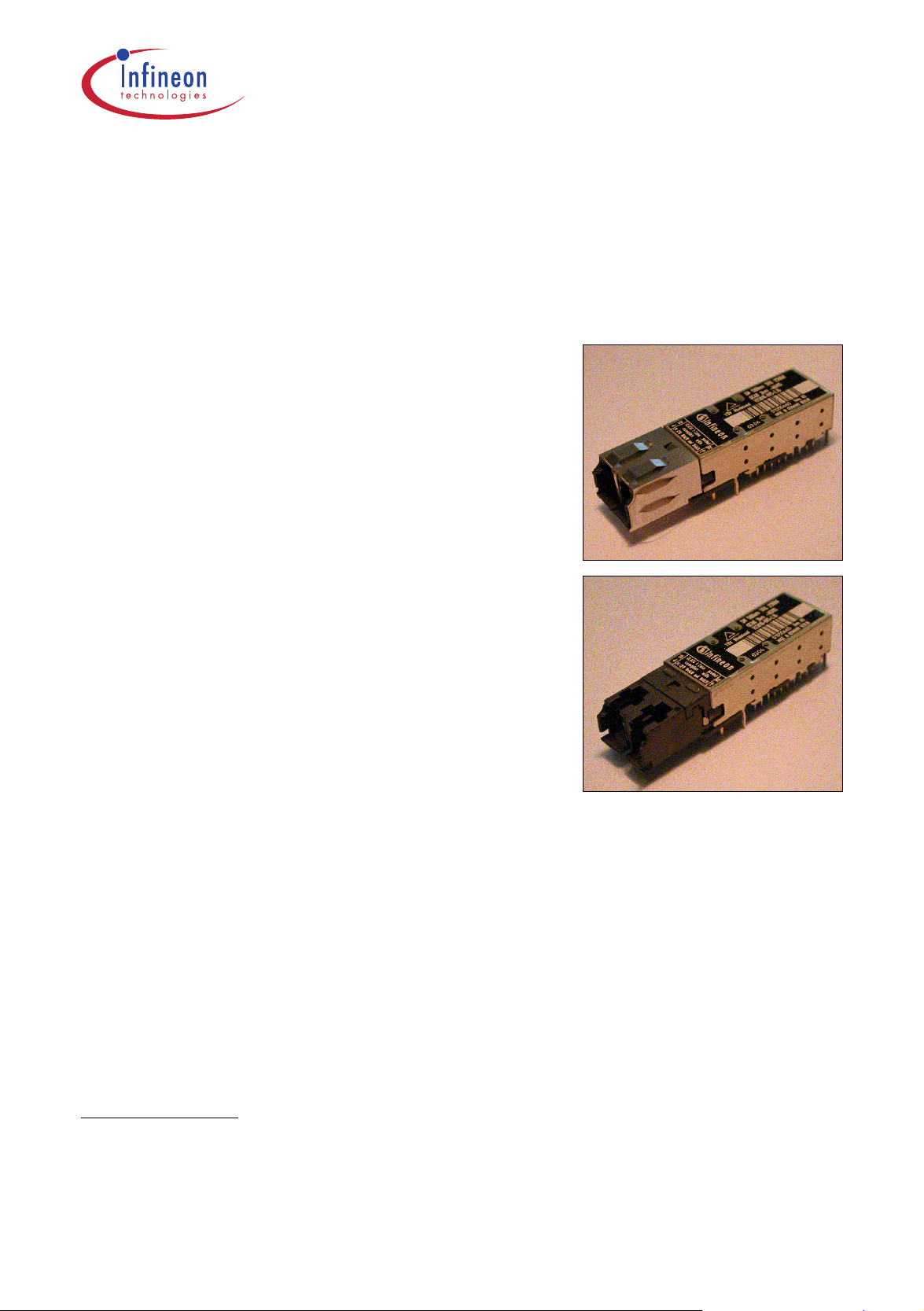
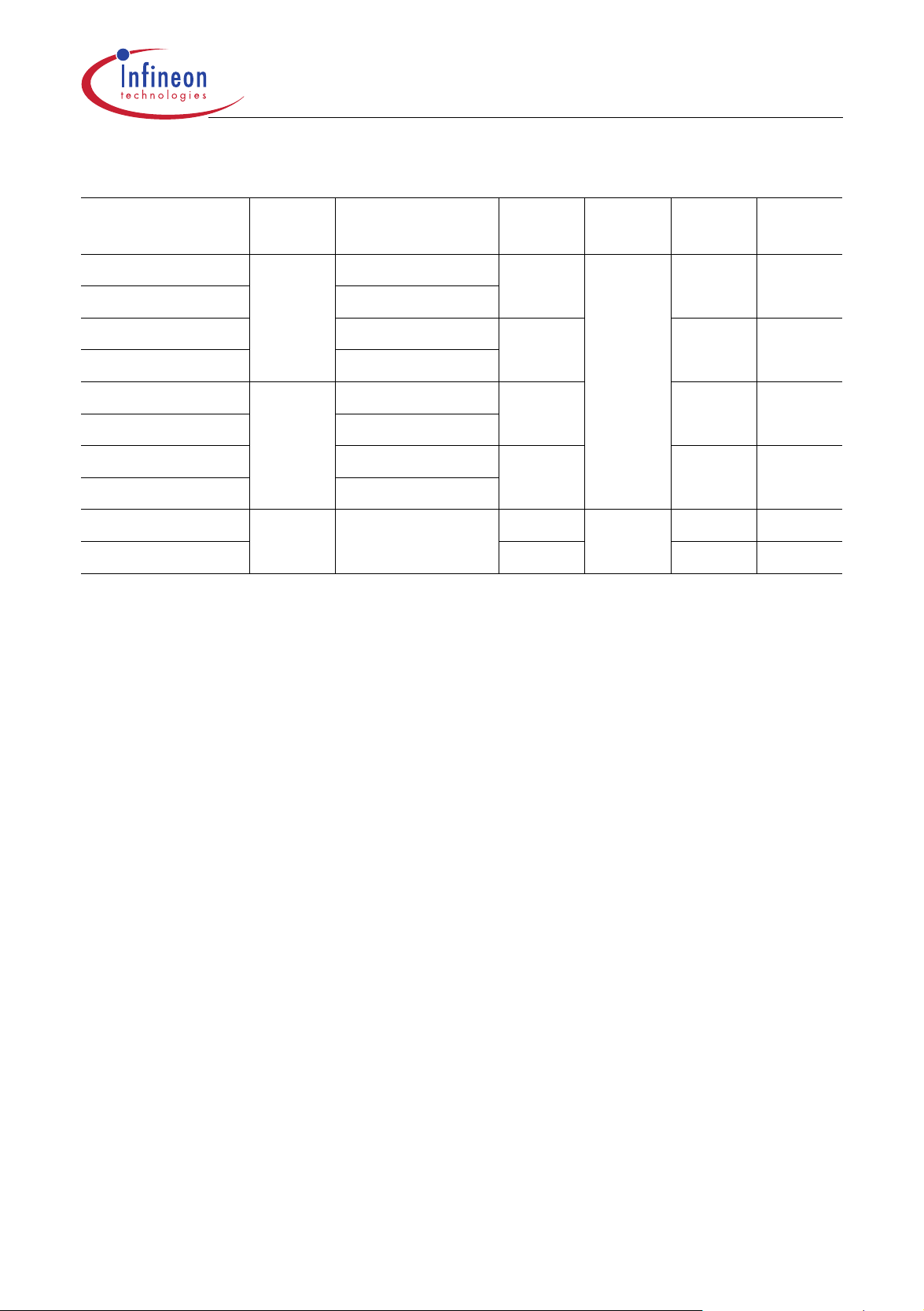
Fiber Optics
Small Form Factor
Single Mode 1300 nm 1.0625 Gbit/s Fibre Channel
1.25 Gigabit Ethernet Transceiver
2x5/2x10 Pinning with LC™ Connector
Preliminary Data
Features
• Small Form Factor transceiver
• Complies with Fibre Channel and Gigabit Ethernet
standards
• RJ-45 style LC™ connector system
• Available with or without collar
• Half the size of SC Duplex 1x9 transceiver
• Single power supply (3.3 V)
• Low power consumption, 650 mW typical
• Loss of optical signal indicator
V23818-K15-Lxx
File: 1119
• Laser disable input
• LVPECL differential inputs and outputs
• AC/AC coupling in accordance to SFF MSA or optional
DC/DC coupling version
• For distance of up to 10 km on single mode fiber
(SMF)
• Class 1 FDA and IEC laser safety compliant
• Multisource 2x5/2x10 footprint
1)
• Small size for high port density
• UL 94 V-0 certified
• Compliant with FCC (Class B) and EN 55022
• Tx and Rx power monitor on 2x10 pinning version
File: 1120
1)
Current MSA documentation can be found at www.infineon.com/fiberoptics
For ordering information see next page.
LC™ is a trademark of Lucent.
Data Sheet 1 2003-03-21
V23818-K15-Lxx
Ordering Information
Ordering Information
Part Number Pinning Temperature
Range
Signal
Detect
Collar Input Output
V23818-K15-L37 2x5 0°C to 70°C LVPECL yes DC DC
V23818-K15-L36 –40°C to 85°C
V23818-K15-L47 0°C to 70°C LVTTL AC AC
V23818-K15-L46 –40°C to 85°C
V23818-K15-L17 2x10 0°C to 70°C LVPECL DC DC
V23818-K15-L16 –40°C to 85°C
V23818-K15-L57 0°C to 70°C LVTTL AC AC
V23818-K15-L56 –40°C to 85°C
V23818-K15-L35 2x5 0°C to 70°C LVPECL no DC DC
V23818-K15-L45 LVTTL AC AC
Data Sheet 2 2003-03-21
V23818-K15-Lxx
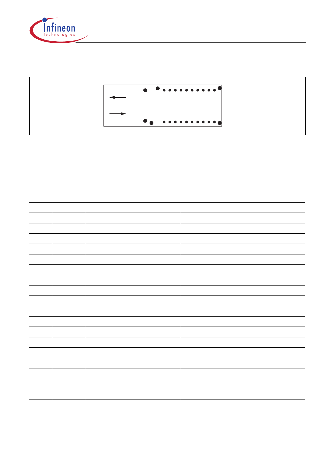
Pin Configuration
Pin Configuration
Tx
Rx
MS
MS
HL
TOP VIEW
12345
HL
1617181920
678910
HL
1112131415
HL
File: 1335
Figure 1 2x10 Pin Connect Diagram
2x10 Pin Description
Pin
Symbol Level/Logic Description
No.
1 PDBias DC current PIN photo detector bias current
2
3
V
V
EEr
EEr
Ground Receiver signal ground
Ground Receiver signal ground
4 NC Not connected
5 NC Not connected
6
7
V
V
EEr
CCr
8 SD LVTTL or LVPECL output
Ground Receiver signal ground
Power supply Receiver power supply
1)
Receiver optical input level monitor
9 RD– LVPECL output Receiver data out bar
10 RD+ LVPECL output Receiver data out
11
12
V
V
CCt
EEt
Power supply Transmitter power supply
Ground Transmitter signal ground
13 TDis LVTTL input Transmitter disable
14 TD+ LVPECL input Transmitter data in
15 TD– LVPECL input Transmitter data in bar
16
V
EEt
Ground Transmitter signal ground
17 BMon– DC voltage Laser diode bias current monitor
18 BMon+ DC voltage Laser diode bias current monitor
19 PMon– DC voltage Laser diode optical power monitor
20 PMon+ DC voltage Laser diode optical power monitor
MS Mounting studs
HL Housing leads
1)
LVPECL output active high for V23818-K15-L17/L16.
LVTTL output active high for V23818-K15-L57/L56.
Data Sheet 3 2003-03-21
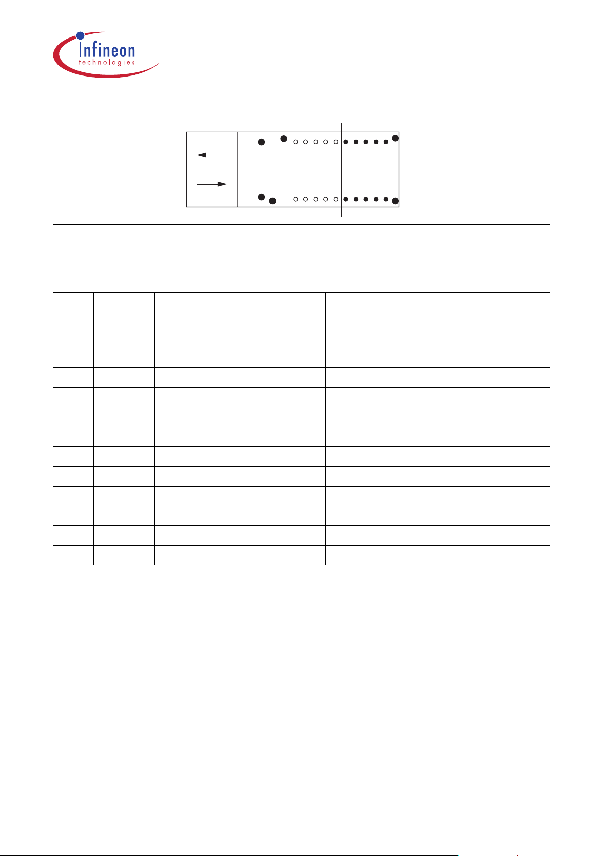
V23818-K15-Lxx
Tx
Rx
MS
MS
HL
TOP VIEW
HL
Figure 2 2x5 Pin Connect Diagram
2x5 Pin Description
Pin
Symbol Level/Logic Description
No.
1
2
V
V
EEr
CCr
Ground Receiver signal ground
Power supply Receiver power supply
3 SD LVTTL or LVPECL output
Pin Configuration
HL
678910
12345
1)
Receiver optical input level monitor
HL
File: 1331
4 RD– LVPECL output Receiver data out bar
5 RD+ LVPECL output Receiver data out
6
7
V
V
CCt
EEt
Power supply Transmitter power supply
Ground Transmitter signal ground
8 TDis LVTTL input Transmitter disable
9 TD+ LVPECL input Transmitter data in
10 TD– LVPECL input Transmitter data in bar
MS Mounting studs
HL Housing leads
1)
LVPECL output active high for V23818-K15-L37/L36/L35.
LVTTL output active high for V23818-K15-L47/L46/L45.
V
/ V
EEr
EEt
For 2x10 transceivers, connect pins 2, 3, 6, 12 and 16 to signal ground. For 2x5
transceivers, connect pins 1 and 7 to signal ground.
Data Sheet 4 2003-03-21

V23818-K15-Lxx
V
CCr
/ V
CCt
Pin Configuration
For 2x10 transceivers a 3.3 V DC power supply must be applied at pins 7 and 11. For
2x5 transceivers a 3.3 V
DC power supply must be applied at pins 2 and 6. A
recommended power supply filter network is given in the termination scheme. Locate
power supply filtering directly at the transceiver power supply pins. Proper power supply
filtering is essential for good EMI performance.
TD+ / TD–
Transmitter data LVPECL level inputs. For V23818-K15-L47/L46/L57/L56/L45
terminated and AC coupled internally. For V23818-K15-L37/L36/L17/L16/L35 use
termination and coupling as shown in the termination scheme.
RD– / RD+
Receiver data LVPECL level outputs. For V23818-K15-L47/L46/L57/L56/L45 biased and
AC coupled internally. For V23818-K15-L37/L36/L17/L16/L35 use termination and
coupling as shown in the termination scheme.
TDis
A logical LVTTL high input will disable the laser. To enable the laser, an LVTTL low input
must be applied. Leave pin unconnected if feature not required.
SD
LVTTL output for V23818-K15-L47/L46/L57/L56/L45.
LVPECL output for V23818-K15-L37/L36/L17/L16/L35.
A logical high output indicates normal optical input levels to the receiver. Low optical
input levels at the receiver result in a low output. Signal Detect can be used to determine
a definite optical link failure; break in fiber, unplugging of a connector, faulty laser source.
However it is not a detection of a bad link due to data-related errors.
MS
Mounting studs are provided for transceiver mechanical attachment to the circuit board.
They also provide an optional connection of the transceiver to the equipment chassis
ground. The holes in the circuit board must be tied to chassis ground.
HL
Housing leads are provided for additional signal grounding. The holes in the circuit board
must be included and tied to signal ground.
Data Sheet 5 2003-03-21
V23818-K15-Lxx
Pin Configuration
2x10 Transceiver Additional Functionality
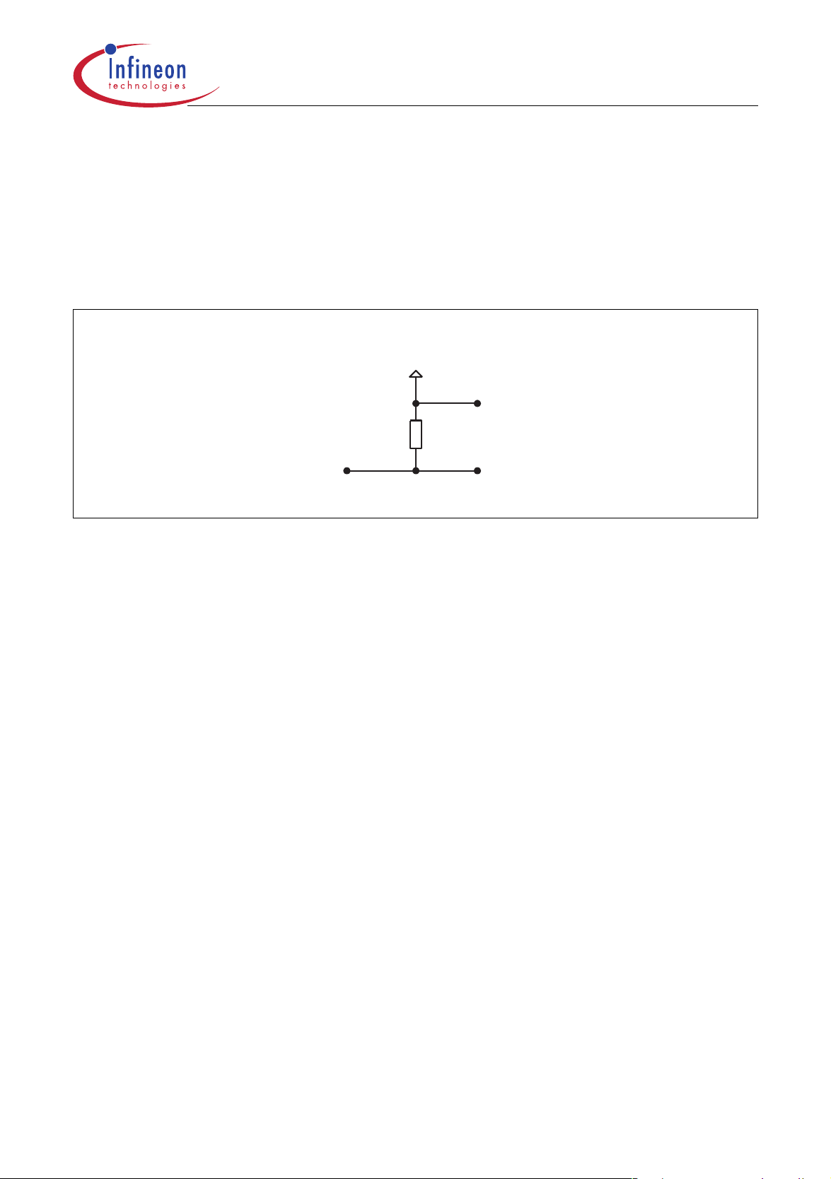
PDBias
Connect pin 1 to
V
through a bias resistor, of a value not exceeding 2 kΩ, as shown in
CC
Figure 3 to monitor PIN photo detector bias current. Leave pin floating if not used.
Typical behaviour is shown in Figure 4 and Figure 5 using a 2 kΩ load.
V
CC
≤ 2 kΩ
Pin 1
V
bias
File: 1307
Figure 3 Photo Detector Bias Interface
Data Sheet 6 2003-03-21
V23818-K15-Lxx
Pin Configuration
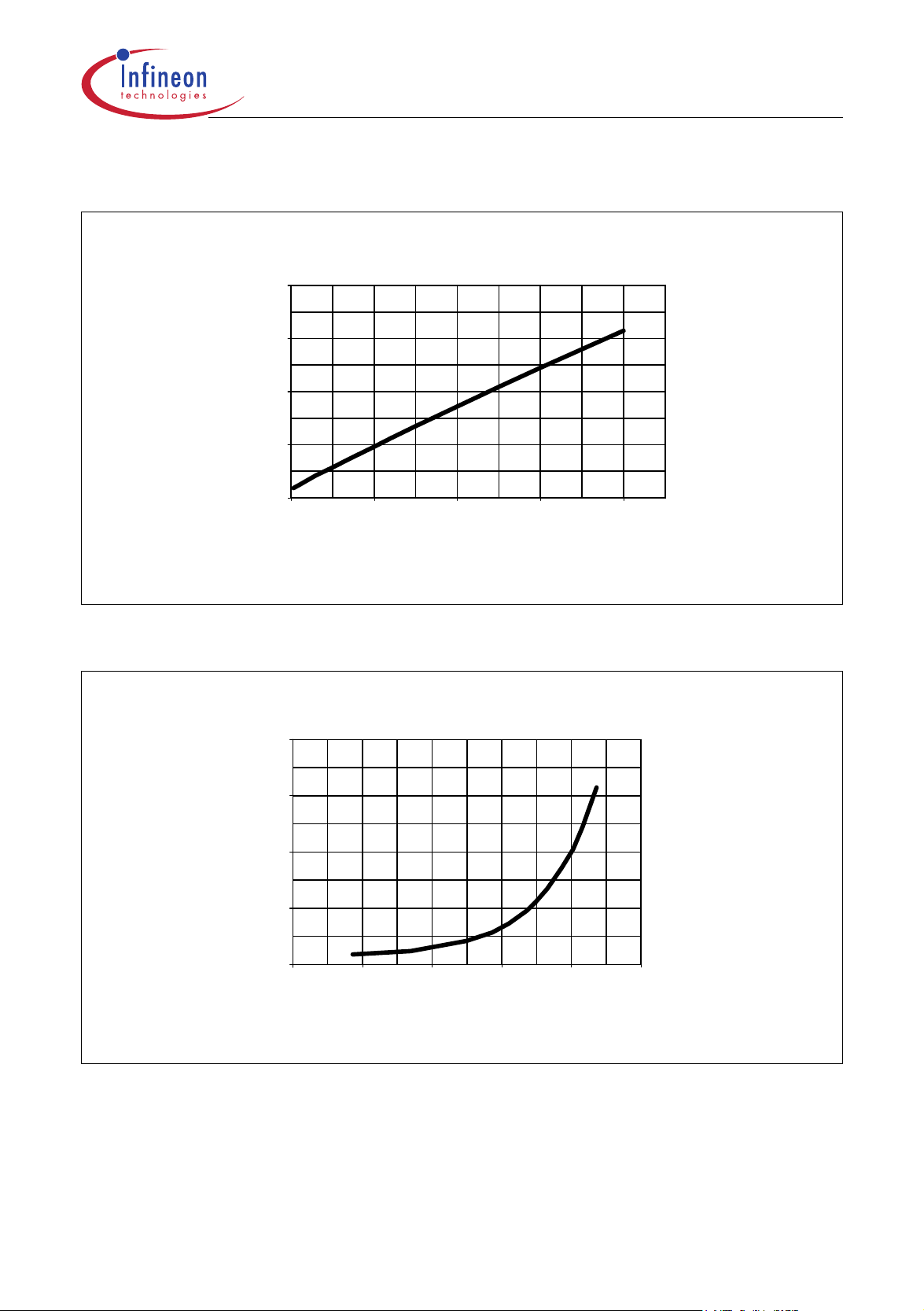
Typical Responsitivity of PIN Photo Detector Bias Current Monitor
400
300
200
100
Photo Detector Monitor Current (µA)
0
0 100 200 300 400
Received Optical Power (µW)
File: 1308
Figure 4 Linear Response
400
300
200
100
Photo Detector Monitor Current (µA)
0
−30 −24 −18 −12 −60
Received Optical Power (dBm)
File: 1309
Figure 5 Logarithmic Response
Data Sheet 7 2003-03-21
V23818-K15-Lxx
0
0.04
0.08
0.12
0.16
0.2
0.24
0.28
0.32
0.36
010203040506070
Temperature (˚C)
BMon Output Voltage (V)
Pin Configuration
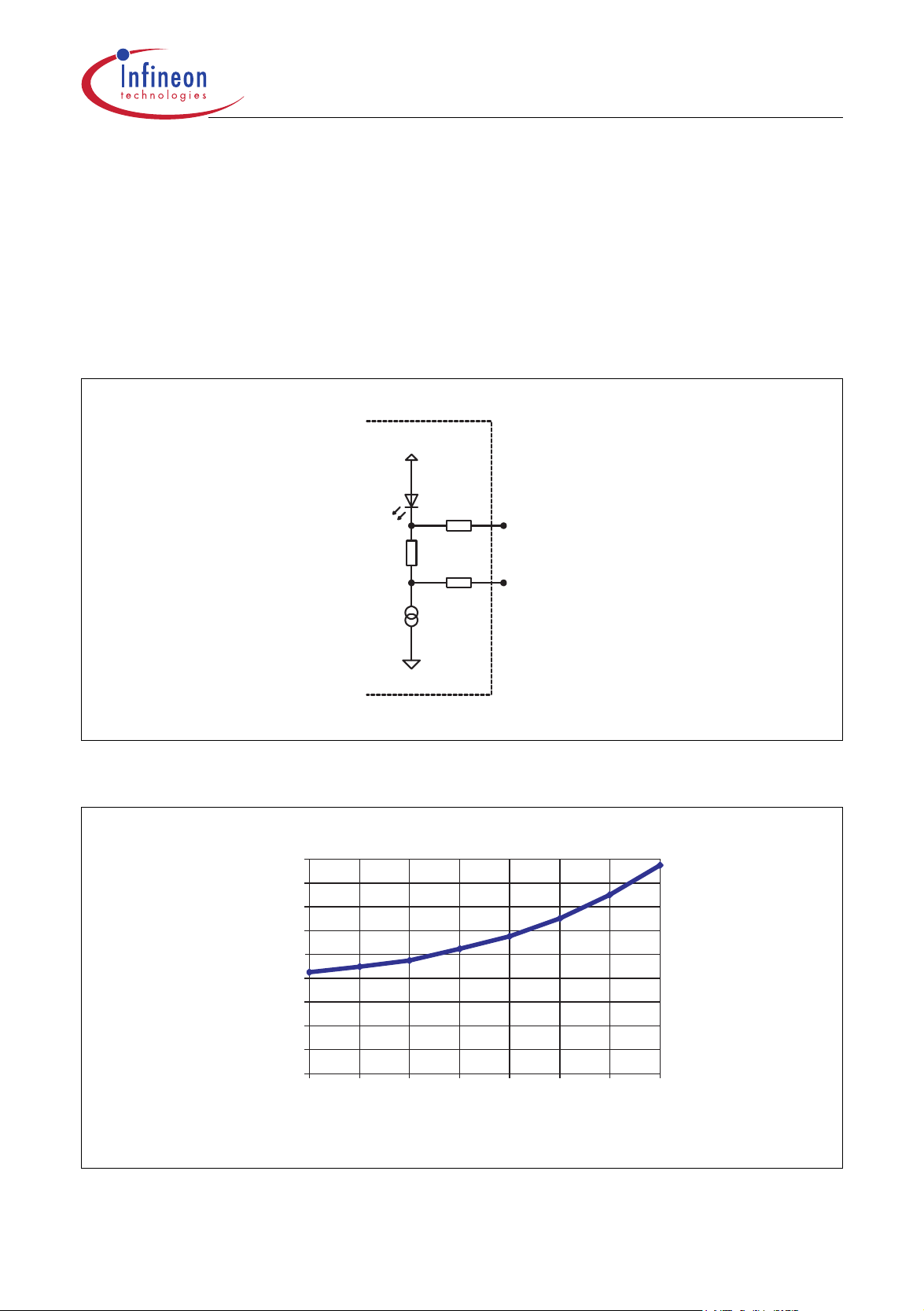
BMon– / BMon+
The DC voltage measured across pins 17 and 18 is proportional to the laser bias current.
Use the equation:
I
bias
= V
bias
/10 Ω
Use this output to monitor laser performance and EOL conditions. A schematic and
typical behaviour are shown in Figure 6 and Figure 7.
I
@ ambient 25°C < 60 mA.
bias
Leave pins floating if function is not required.
V
CC
10 Ω
3 kΩ
3 kΩ
Pin 18
Pin 17
V
EE
Figure 6 Bias Monitor – Transceiver Internal
Figure 7 Typical Variations of Bias Monitor Voltage over Temperature
Data Sheet 8 2003-03-21
File: 1310
File: 1312

V23818-K15-Lxx
Pin Configuration
PMon– / PMon+
This output is derived from the Tx monitor diode. Output voltage is in the range of
1.2 ±0.2 V. Source resistance R
= 100 kΩ.
S
Note: This voltage level is not MSA compliant.
Data Sheet 9 2003-03-21

V23818-K15-Lxx
Description
Description
The Infineon single mode transceiver is based on and compliant to the Physical Medium
Depend (PMD) sublayer and baseband medium, type 1000-Base-LX (long wavelength)
as specified in IEEE Std 802.3 and Fibre Channel FC-PI Rev. 13 100-SM-LC-L.
The appropriate fiber optic cable is 9 µm single mode fiber with LC connector.
The Infineon single mode transceiver is a single unit comprised of a transmitter, a
receiver, and an LC receptacle. This design frees the customer from many alignment
and PC board layout concerns.
This transceiver supports the LC connectorization concept, which competes with UTP/
CAT 5 solutions. It is compatible with RJ-45 style backpanels for fiber-to-the-desktop
applications while providing the advantages of fiber optic technology. The receptacle
accepts the new LC connector. The Small Form Factor is specially developed for
distances of up to 10 km.
The module is designed for low cost LAN and WAN applications. It can be used as the
network end device interface in mainframes, workstations, servers, and storage devices,
and in a broad range of network devices such as bridges, routers, hubs, and local and
wide area switches.
This transceiver operates at 1.0625 and 1.25 Gbit/s from a single power supply. The full
differential data inputs and outputs are LVPECL compatible.
Functional Description of SFF Transceiver
This transceiver is designed to transmit serial data via single mode fiber.
BMon
-
BMon+
Automatic
TDis
TD
TD+
PMon
PMon+
RD
RD+
SD
Shut-Down
3k3k3k
-
-
-
Laser
Driver
Power
Control
Receiver
200
10
3k
Tx
Coupling Unit
e/o
Laser
o/e
Monitor
Rx
Coupling Unit
o/e
Single
Mode
Fiber
PDBias
File: 1357
Figure 8 Functional Diagram 2x10 Pin Rows
Data Sheet 10 2003-03-21

V23818-K15-Lxx
Automatic
TDis
TD−
TD+
RD−
RD+
SD
Shut-Down
Laser
Driver
Power
Control
Limiting
Amp
Tx
Coupling Unit
Rx
Coupling Unit
TIA
e/o
Laser
o/e
Monitor
o/e
Single
Mode
Fiber
Description
File: 1351
Figure 9 Functional Diagram 2x5 Pin Rows
The receiver component converts the optical serial data into an electrical data (RD+ and
RD–). The Signal Detect output (SD) shows whether an optical signal is present.
The transmitter part converts electrical LVPECL compatible serial data (TD+ and TD–)
into optical serial data.
The module has an integrated shutdown function that switches the laser off in the event
of an internal failure.
Reset is only possible if the power is turned off, and then on again. (
V
).
TH
V
switched below
CCt
The transmitter contains a laser driver circuit that drives the modulation and bias current
of the laser diode. The currents are controlled by a power control circuit to guarantee
constant output power of the laser over temperature and aging. The power control uses
the output of the monitor PIN diode (mechanically built into the laser coupling unit) as a
controlling signal, to prevent the laser power from exceeding the operating limits.
Data Sheet 11 2003-03-21

V23818-K15-Lxx
Regulatory Compliance
Feature Standard Comments
ESD:
Electrostatic Discharge to
the Electrical Pins
Immunity:
Against Electrostatic
Discharge (ESD) to the
Duplex LC Receptacle
Immunity:
Against Radio Frequency
Electromagnetic Field
EIA/JESD22-A114-B
(MIL-STD 883D
Method 3015.7)
EN 61000-4-2
IEC 61000-4-2
EN 61000-4-3
IEC 61000-4-3
Class 1C
Discharges ranging from ±2 kV to
±15 kV on the receptacle cause no
damage to transceiver (under
recommended conditions).
With a field strength of 3 V/m, noise
frequency ranges from 10 MHz to
2 GHz. No effect on transceiver
performance between the
specification limits.
Emission:
Electromagnetic
Interference (EMI)
FCC 47 CFR Part 15,
Class B
EN 55022 Class B
Noise frequency range:
30 MHz to 18 GHz
CISPR 22
Description
(13.97)
*) min. pitch between SFF transceiver according to MSA.
Dimensions in (mm) inches File: 1501
*)
.550
Figure 10 Transceiver Pitch
Data Sheet 12 2003-03-21

V23818-K15-Lxx
Technical Data
Technical Data
Absolute Maximum Ratings
Parameter Symbol Limit Values Unit
min. max.
Package Power Dissipation 0.95 W
Supply Voltage
Data Input Levels
Differential Data Input Voltage Swing
V
CC–VEE
V
+0.5 VEE–0.5 V
CC
V
pk-pk 5 V
ID
4V
Storage Ambient Temperature –40 85 °C
Hand Lead Soldering Temp/Time 260/10 °C/s
Wave Soldering Temp/Time 260/10 °C/s
Aqueous Wash Pressure < 110 psi
Exceeding any one of these values may destroy the device immediately.
Data Sheet 13 2003-03-21

V23818-K15-Lxx
Technical Data
Recommended Operating Conditions
Parameter Symbol Limit Values Unit
min. typ. max.
Ambient Temperature
Ambient Temperature
Power Supply Voltage
1), 3)
2), 3)
T
AMB
V
CC–VEE
–40 85 °C
070
3.14 3.3 3.46 V
Transmitter
Data Input High Voltage DC/DC
Differential Data Input Voltage
V
IH–VCC
V
pk-pk 500 3200 mV
ID
–1165 –880 mV
Swing AC/AC
Data Input Low Voltage DC/DC V
Data Input Rise/Fall Time
Supply Current Tx
t
I
IL–VCC
i
CCt
–1810 –1475 mV
120 ps
140 mA
Receiver
Input Center Wavelength λ
Supply Current Rx
1)
For V23818-K15-L36/L46/L16/L56.
2)
For V23818-K15-L37/L47/L17/L57/L35/L45.
3)
Ambient operating temperature requires a 2 ms–1 airflow over the device.
I
Rx
CCr
1260 1580 nm
130 mA
The electro-optical characteristics described in the following tables are valid only for use
under the recommended operating conditions.
Data Sheet 14 2003-03-21

V23818-K15-Lxx
Technical Data
Transmitter Electro-Optical Characteristics
Parameter Symbol Limit Values Unit
min. typ. max.
Output Power (Average)
1)
Center Wavelength λ
P
O
C
–9.5 –3 dBm
1270 1355 nm
Spectral Width (RMS) σ 4nm
Extinction Ratio (Dynamic) ER 9 dB
Reset Threshold for
Power on Delay
2)
V
CCt
2)
V
t
DEL
TH
2.7 V
30 ms
Total Tx Jitter TJ 53 130 ps
T
Assert Voltage LVTTL V
Dis
T
Deassert Voltage LVTTL V
Dis
T
Assert Time
Dis
T
Deassert Time
Dis
1)
Into single mode fiber, 9 µm diameter
2)
Laser power is shut down if power supply is below VTH and switched on if power supply is above VTH after t
3)
T
assertion to laser shutdown.
Dis
4)
T
reassertion to laser startup.
Dis
3)
4)
t
ASS
t
DAS
TDH
TDL
2V
0.8 V
0.4 1 ms
0.06 10 µs
.
RES
Receiver Electro-Optical Characteristics
Parameter Symbol Limit Values Unit
min. typ. max.
Sensitivity (Average Power)
Saturation (Average Power)
Min. Optical Modulation
Amplitude
2)
Signal Detect Assert Level
Signal Detect Deassert Level
Signal Detect Hysteresis
Signal Detect Assert Time
Signal Detect Deassert Time
Receiver 3 dB Cut off
Frequency
2)
1)
P
P
IN
SAT
–20 dBm
–3 dBm
OMA 15 µW
3)
3)
2), 4)
4)
P
P
P
–P
t
ASS
t
DAS
SDA
SDD
SDA
SDD
–20 dBm
–37 dBm
3dB
0.1 ms
0.35 ms
1.5 GHz
Data Sheet 15 2003-03-21

V23818-K15-Lxx
Technical Data
Receiver Electro-Optical Characteristics (cont’d)
Parameter Symbol Limit Values Unit
min. typ. max.
Receiver 10 dB Cut off
Frequency
Output Voltage
Output Voltage
2)
5)
5)
Differential Data Output Voltage
Swing
5)
Signal Detect Output High
Voltage LVPECL
6), 7)
Signal Detect Output Low
Voltage LVPECL
6), 7)
Signal Detect Output High
Voltage LVTTL
6), 8)
V
OH–VCC
V
OL–VCC
V
pk-pk 1000 2000 mV
OD
V
SDH–VEEVCC
V
SDL–VEEVCC
V
SDH
–1110 –650 mV
–1800 –1300 mV
–
1200
–
1900
2.4 V
3GHz
V
CC
mV
–820
V
CC
–
1580
mV
Signal Detect Output Low
Voltage LVTTL
Rx-Monitor
1)
Minimum average optical power at which the BER is less than 1x10
2)
Fibre Channel PI Standard.
3)
An increase in optical power above the specified level will cause the Signal Detect to switch from a low state
to a high state (high active output).
4)
A decrease in optical power below the specified level will cause the Signal Detect to switch from a high state
to a low state.
5)
Load is 100 Ω differential.
6)
Internal load is 510 Ω to GND, no external load necessary. Signal Detect is a high active output. High level
means signal is present, low level means loss of signal.
7)
For V23818-K15-L37/L36/L17/L16/L35.
8)
For V23818-K15-L47/L46/L57/L56/L45.
9)
Monitor current needs to be sunk to VCC.
10)
Only available on 2x10 transceivers: V23818-K15-L17/L16/L57/L56.
6), 8)
9), 10)
V
SDL
Rx-Mon 0.5 1 A/W
–10
. Measured with a 2
0.5 V
7
–1 NRZ PRBS.
Data Sheet 16 2003-03-21

V23818-K15-Lxx
Eye Safety
Eye Safety
This laser based single mode transceiver is a Class 1 product.
It complies with IEC 60825-1 and FDA 21 CFR 1040.10 and 1040.11.
To meet laser safety requirements the transceiver shall be operated within the Absolute
Maximum Ratings.
Attention: All adjustments have been made at the factory prior to shipment of the
devices. No maintenance or alteration to the device is required.
Tampering with or modifying the performance of the device will result
in voided product warranty.
Note: Failure to adhere to the above restrictions could result in a modification that is
considered an act of “manufacturing”, and will require, under law, recertification of
the modified product with the U.S. Food and Drug Administration (ref. 21 CFR
1040.10 (i)).
Laser Data
Wavelength 1300 nm
Total output power
< 2 mW
(as defined by IEC: 7 mm aperture at 14 mm distance)
Total output power
< 180 µW
(as defined by FDA: 7 mm aperture at 20 cm distance)
Beam divergence 6°
FDA
Complies with 21 CFR
1040.10 and 1040.11
Class 1 Laser Product
IEC
Figure 11 Required Labels
Indication of
laser aperture
and beam
Tx
Rx
20 19 18 17 16 15 14 13 12 11
Top view
12345678910
File: 1401
File: 1334
Figure 12 Laser Emission
Data Sheet 17 2003-03-21

V23818-K15-Lxx
EMI-Recommendations
EMI-Recommendations
To avoid electromagnetic radiation exceeding the required limits please take note of the
following recommendations.
When Gigabit switching components are found on a PCB (multiplexers, clock recoveries
etc.) any opening of the chassis may produce radiation also at chassis slots other than
that of the device itself. Thus every mechanical opening or aperture should be as small
as possible.
On the board itself every data connection should be an impedance matched line (e.g.
strip line, coplanar strip line). Data, Datanot should be routed symmetrically, vias should
be avoided. A terminating resistor of 100 Ω should be placed at the end of each matched
line. An alternative termination can be provided with a 50 Ω resistor at each (D, Dn). In
DC coupled systems a thevenin equivalent 50 Ω resistance can be achieved as follows:
for 3.3 V: 125 Ω to
V
and 82 Ω to VEE, for 5 V: 82 Ω to VCC and 125 Ω to VEE at Data
CC
and Datanot. Please consider whether there is an internal termination inside an IC or a
transceiver.
In certain cases signal GND is the most harmful source of radiation. Connecting chassis
GND and signal GND at the plate/bezel/chassis rear e.g. by means of a fiber optic
transceiver may result in a large amount of radiation. Even a capacitive coupling
between signal GND and chassis may be harmful if it is too close to an opening or an
aperture.
If a separation of signal GND and chassis GND is not planned, it is strongly
recommended to provide a proper contact between signal GND and chassis GND at
every location where possible. This concept is designed to avoid hotspots. Hotspots are
places of highest radiation which could be generated if only a few connections between
signal and chassis GND exist. Compensation currents would concentrate at these
connections, causing radiation.
By use of Gigabit switching components in a design, the return path of the RF current
must also be considered. Thus a split GND plane of Tx and Rx portion may result in
severe EMI problems.
A recommendation is to connect the housing leads to signal GND. However, in certain
applications it may improve EMI performance by connecting them to chassis GND.
The cutout should be sized so that all contact springs make good contact with the face
plate.
Please consider that the PCB may behave like a waveguide. With an ε
of 4, the
r
wavelength of the harmonics inside the PCB will be half of that in free space. In this
scenario even the smallest PCBs may have unexpected resonances.
Data Sheet 18 2003-03-21

V23818-K15-Lxx
Recommended Termination Schemes
2x10 DC/DC Transceiver
PMon+
PMon−
BMon−
BMon+
18
1720 19
12,16
V
EEt
14
TD+
Laser
Driver
SFF Transceiver
PreAmp
Limiting
Amplifier
100 Ω
Signal
Detect
RD−
RD+
TD−
TDis
V
CCt
V
CCr
SD
RD−
RD+
V
EEr
15
13
11
7
8
1
9
10
2,3,6
C8
C9
Recommended Termination Schemes
TDis
C1
C2
PDBias
R2
R3
SD
VCC SerDes
C6
C7
L1
V
CC
3.3 V
L2
C3
C4
C5
R4
C10
R5
R1
V
CC
SerDat Out
SerDat Out −
Serializer/
Deserializer
SerDat In −
SerDat In +
+
ECL/
PECL
Driver
Receiver
PLL etc.
C1/2/3
C4/5/6/7
C8/9/10
L1/2
R1
= 4.7 ... 10 µF
= 100 nF
= Design criterion is the resonance frequency only. The self resonant frequency of the
capacitor must be in the vicinity of the nominal data rate. Short traces are mandatory.
*)
= 1 ... 4.7 µH
= 100 Ω (depending on SerDes chip used, ensure proper 50 Ω termination to V
EE
or
100 Ω differential is provided. Check for termination inside of SerDes chip).
R2/3
R4/5
= 150 Ω
= Biasing (depends on SerDes chip).
Place R1/4/5 close to SerDes chip.
Place R2/3 close to Infineon transceiver.
*)
The inductors may be replaced by appropriate Ferrite beads.
File: 1390
Figure 13
Data Sheet 19 2003-03-21

V23818-K15-Lxx
2x10 AC/AC Transceiver
PMon+
PMon−
BMon−
BMon+
20 18
1719
PreAmp
Laser
Driver
SFF Transceiver
100 Ω
Limiting
Amplifier
Signal
Detect
V
TD+
TD−
TDis
V
CCt
V
CCr
SD
RD−
RD+
V
EEt
EEt
12,16
14
15
13
11
7
8
1
9
10
2,3,6
C4
C5
Recommended Termination Schemes
VCC SerDes
V
CC
SerDat Out +
SerDat Out −
TDis
C1
C2
PDBias
SD
L1
V
CC
3.3 V
L2
C3
C6
R1
R5
R3
R6
Serializer/
Deserializer
R2
SerDat In −
SerDat In +
R4
ECL/
PECL
Driver
Receiver
PLL etc.
C1/2/3
C4/5/6
L1/2
R1/2/3/4
= 4.7 ... 10 µF
= Design criterion is the resonance frequency only. The self resonant frequency of the
capacitor must be in the vicinity of the nominal data rate. Short traces are mandatory.
*)
= 1 ... 4.7 µH
= Depends on SerDes chip used, ensure proper 50 Ω termination to V
differential is provided. Check for termination inside of SerDes chip.
R5/6
= Biasing (depends on SerDes chip).
Place R1/2/3/4/5/6 close to SerDes chip.
*)
The inductors may be replaced by appropriate Ferrite beads.
Figure 14
or 100 Ω
EE
File: 1391
Data Sheet 20 2003-03-21

V23818-K15-Lxx
2x5 DC/DC Transceiver
Laser
Driver
SFF Transceiver
PreAmp
Limiting
Amplifier
100 Ω
Signal
Detect
RD−
RD+
V
TD+
TD−
TDis
V
V
CCr
SD
RD−
RD+
EEt
CCt
Recommended Termination Schemes
V
CC
3.3 V
C3
VCC SerDes
C6
C7
C10
R4
R5
R1
V
CC
SerDat Out
SerDat Out −
Serializer/
Deserializer
SerDat In −
SerDat In +
+
ECL/
PECL
Driver
Receiver
PLL etc.
7
9
C8
10
8
6
2
3
4
5
C9
TDis
C1
C2
L1
L2
SD
C4
C5
1
V
EEr
C1/2/3
C4/5/6/7
C8/9/10
L1/2
R1
= 4.7 ... 10 µF
= 100 nF
= Design criterion is the resonance frequency only. The self resonant frequency of the
capacitor must be in the vicinity of the nominal data rate. Short traces are mandatory.
*)
= 1 ... 4.7 µH
= 100 Ω (depending on SerDes chip used, ensure proper 50 Ω termination to V
100 Ω differential is provided. Check for termination inside of SerDes chip).
R2/3
R4/5
= 150 Ω
= Biasing for outputs depending on Serializer.
Place R1/4/5 close to SerDes chip.
Place R2/3 close to Infineon transceiver.
*)
The inductors may be replaced by appropriate Ferrite beads.
Figure 15
R2
R3
EE
or
File: 1392
Data Sheet 21 2003-03-21

V23818-K15-Lxx
2x5 AC/AC Transceiver
Laser
Driver
SFF Transceiver
PreAmp
Limiting
Amplifier
100 Ω
Signal
Detect
RD−
RD+
V
EEt
TD+
TD−
TDis
V
CCt
V
CCr
SD
RD−
RD+
Recommended Termination Schemes
VCC SerDes
7
9
C4
10
8
TDis
6
C1
2
C2
3
4
C5
5
SD
L1
V
CC
3.3 V
L2
C3
C6
R5
R1
R6
R2
V
CC
SerDat Out
SerDat Out −
Serializer/
Deserializer
SerDat In −
SerDat In +
+
ECL/
PECL
Driver
Receiver
PLL etc.
1
V
EEr
C1/2/3
C4/5/6
L1/2
R1/2/3/4
R5/6
= 4.7 ... 10 µF
= Design criterion is the resonance frequency only. The self resonant frequency of the
capacitor must be in the vicinity of the nominal data rate. Short traces are mandatory.
*)
= 1 ... 4.7 µH
= Depends on SerDes chip used, ensure proper 50 Ω termination to V
differential is provided. Check for termination inside of SerDes chip.
= Biasing (depends on SerDes chip).
Place R1/2/3/4/5/6 close to SerDes chip.
*)
The inductors may be replaced by appropriate Ferrite beads.
Figure 16
R3
R4
or 100 Ω
EE
File: 1393
Data Sheet 22 2003-03-21

V23818-K15-Lxx
Package Outlines
Package Outlines
a) recommended bezel position
Drawing shown is 2x10 pinning with collar
Dimensions in mm [inches] File: 1213
Figure 17
Data Sheet 23 2003-03-21

V23818-K15-Lxx
Revision History: 2003-03-21 DS2
Previous Version: 2003-03-05
Page Subjects (major changes since last revision)
15 Table "Transmitter Electro-Optical Characteristics" changed
For questions on technology, delivery and prices please contact the Infineon
Technologies Offices in Germany or the Infineon Technologies Companies and
Representatives worldwide: see our webpage at http://www.infineon.com.
Edition 2003-03-21
Published by Infineon Technologies AG,
St.-Martin-Strasse 53,
D-81541 München, Germany
© Infineon Technologies AG 2003.
All Rights Reserved.
Attention please!
The information herein is given to describe certain components and shall not be considered as warranted
characteristics.
Terms of delivery and rights to technical change reserved.
We hereby disclaim any and all warranties, including but not limited to warranties of non-infringement, regarding
circuits, descriptions and charts stated herein.
Infineon Technologies is an approved CECC manufacturer.
Information
For further information on technology, delivery terms and conditions and prices please contact your nearest
Infineon Technologies Office in Germany or our Infineon Technologies Representatives worldwide.
Warnings
Due to technical requirements components may contain dangerous substances. For information on the types in
question please contact your nearest Infineon Technologies Office.
Infineon Technologies Components may only be used in life-support devices or systems with the express written
approval of Infineon Technologies, if a failure of such components can reasonably be expected to cause the failure
of that life-support device or system, or to affect the safety or effectiveness of that device or system. Life-support
devices or systems are intended to be implanted in the human body, or to support and/or maintain and sustain
and/or protect human life. If they fail, it is reasonable to assume that the health of the user or other persons may
be endangered.
 Loading...