

Page 1

Please read the Important notice and the Safety precautions and the Warnings
www.infineon.com page 1 of 37 2020-11-03
UG-2020-31
11 kW bi-directional CLLC DC-DC converter with
1200 V and 1700 V CoolSiC™ MOSFETs
About this document
Scope and purpose
This document introduces a complete Infineon Technologies AG system solution for an 11 kW bi-directional DCDC converter. The REF-DAB11KIZSICSYS board is a DC-DC stage with a wide range output using two inductors
and two capacitors (CLLC) resonant network with bi-directional capability.This converter can operate under
high power conversion efficiency, as the symmetric CLLC resonant network has zero-voltage switching
capability for primary power switches and synchronous-rectification commutation capability for secondry-side
output rectifiers. The converter could change the power flow direction, and its maximum power conversion
efficiency was around 98% during the operation.
This document shows the board using 1200 V CoolSiC™ MOSFETs in TO247-4 package and EiceDRIVER™ 1ED
compact gate driver ICs, which leverage the advantages of SiC technology including improved efficiency, space
and weight savings, part count reduction, and enhanced system reliability.
Intended audience
This document is intended for engineers who want to use 1200 V and 1700 V CoolSiC™ MOSFETs with
EiceDRIVER™ driver ICs for bi-directional resonant topology applications such as EV-charger wall box, energy
storage systems to achieve reliable main-circuit design and increased power density.
Reference board/kit
Product(s) embedded in a PCB, with focus on specific applications and defined use cases that can include
software. PCB and auxiliary circuits are optimized for the requirements of the target application.
Note: Boards do not necessarily meet safety, EMI, quality standards (for example UL, CE) requirements.
Page 2

2 of 37
2020-11-03
11 kW bi-directional CLLC DC-DC converter with 1200V and 1700V CoolSiC™
MOSFETs
Important notice
Important notice
“Evaluation Boards and Reference Boards” shall mean products embedded on a printed circuit board
(PCB) for demonstration and/or evaluation purposes, which include, without limitation, demonstration,
reference and evaluation boards, kits and design (collectively referred to as “Reference Board”).
Environmental conditions have been considered in the design of the Evaluation Boards and Reference
Boards provided by Infineon Technologies. The design of the Evaluation Boards and Reference Boards
has been tested by Infineon Technologies only as described in this document. The design is not qualified
in terms of safety requirements, manufacturing and operation over the entire operating temperature
range or lifetime.
The Evaluation Boards and Reference Boards provided by Infineon Technologies are subject to functional
testing only under typical load conditions. Evaluation Boards and Reference Boards are not subject to the
same procedures as regular products regarding returned material analysis (RMA), process change
notification (PCN) and product discontinuation (PD).
Evaluation Boards and Reference Boards are not commercialized products, and are solely intended for
evaluation and testing purposes. In particular, they shall not be used for reliability testing or production.
The Evaluation Boards and Reference Boards may therefore not comply with CE or similar standards
(including but not limited to the EMC Directive 2004/EC/108 and the EMC Act) and may not fulfill other
requirements of the country in which they are operated by the customer. The customer shall ensure that
all Evaluation Boards and Reference Boards will be handled in a way which is compliant with the relevant
requirements and standards of the country in which they are operated.
The Evaluation Boards and Reference Boards as well as the information provided in this document are
addressed only to qualified and skilled technical staff, for laboratory usage, and shall be used and
managed according to the terms and conditions set forth in this document and in other related
documentation supplied with the respective Evaluation Board or Reference Board.
It is the responsibility of the customer’s technical departments to evaluate the suitability of the
Evaluation Boards and Reference Boards for the intended application, and to evaluate the completeness
and correctness of the information provided in this document with respect to such application.
The customer is obliged to ensure that the use of the Evaluation Boards and Reference Boards does not
cause any harm to persons or third party property.
The Evaluation Boards and Reference Boards and any information in this document is provided "as is"
and Infineon Technologies disclaims any warranties, express or implied, including but not limited to
warranties of non-infringement of third party rights and implied warranties of fitness for any purpose, or
for merchantability.
Infineon Technologies shall not be responsible for any damages resulting from the use of the Evaluation
Boards and Reference Boards and/or from any information provided in this document. The customer is
obliged to defend, indemnify and hold Infineon Technologies harmless from and against any claims or
damages arising out of or resulting from any use thereof.
Infineon Technologies reserves the right to modify this document and/or any information provided
herein at any time without further notice.
Page 3
3 of 37
2020-11-03
11 kW bi-directional CLLC DC-DC converter with 1200V and 1700V CoolSiC™
MOSFETs
Safety precautions
Safety precautions
Note: Please note the following warnings regarding the hazards associated with development systems.
Table 1 Safety precautions
Warning: The DC link potential of this board is up to 1000 VDC. When measuring voltage
waveforms by oscilloscope, high voltage differential probes must be used. Failure to do
so may result in personal injury or death.
Warning: The evaluation or reference board contains DC bus capacitors which take
time to discharge after removal of the main supply. Before working on the drive
system, wait five minutes for capacitors to discharge to safe voltage levels. Failure to
do so may result in personal injury or death. Darkened display LEDs are not an
indication that capacitors have discharged to safe voltage levels.
Warning: The evaluation or reference board is connected to the grid input during
testing. Hence, high-voltage differential probes must be used when measuring voltage
waveforms by oscilloscope. Failure to do so may result in personal injury or death.
Darkened display LEDs are not an indication that capacitors have discharged to safe
voltage levels.
Warning: Remove or disconnect power from the drive before you disconnect or
reconnect wires, or perform maintenance work. Wait five minutes after removing
power to discharge the bus capacitors. Do not attempt to service the drive until the bus
capacitors have discharged to zero. Failure to do so may result in personal injury or
death.
Caution: The heat sink and device surfaces of the evaluation or reference board may
become hot during testing. Hence, necessary precautions are required while handling
the board. Failure to comply may cause injury.
Caution: Only personnel familiar with the drive, power electronics and associated
machinery should plan, install, commission and subsequently service the system.
Failure to comply may result in personal injury and/or equipment damage.
Caution: The evaluation or reference board contains parts and assemblies sensitive to
electrostatic discharge (ESD). Electrostatic control precautions are required when
installing, testing, servicing or repairing the assembly. Component damage may result
if ESD control procedures are not followed. If you are not familiar with electrostatic
control procedures, refer to the applicable ESD protection handbooks and guidelines.
Caution: A drive that is incorrectly applied or installed can lead to component damage
or reduction in product lifetime. Wiring or application errors such as undersizing the
motor, supplying an incorrect or inadequate AC supply, or excessive ambient
temperatures may result in system malfunction.
Caution: The evaluation or reference board is shipped with packing materials that
need to be removed prior to installation. Failure to remove all packing materials that
are unnecessary for system installation may result in overheating or abnormal
operating conditions.
Page 4

4 of 37
2020-11-03
11 kW bi-directional CLLC DC-DC converter with 1200V and 1700V CoolSiC™
MOSFETs
Table of contents
Table of contents
Contents
About this document ....................................................................................................................... 1
Important notice ............................................................................................................................ 2
Safety precautions .......................................................................................................................... 3
Table of contents ............................................................................................................................ 4
1 The board at a glance .............................................................................................................. 5
1.1 Delivery content ...................................................................................................................................... 6
1.2 Block diagram .......................................................................................................................................... 6
1.3 Main features ........................................................................................................................................... 8
1.4 Board parameters and technical data .................................................................................................... 8
2 System and functional description ........................................................................................... 9
2.1 Commissioning ........................................................................................................................................ 9
2.2 Description of the functional blocks ....................................................................................................... 9
2.2.1 Description of the functional blocks ............................................................................................... 10
2.2.2 Special operation modes ................................................................................................................. 15
2.3 Auxiliary power boards ......................................................................................................................... 17
2.3.1 The technical specification of auxiliary power boards ................................................................... 17
2.3.2 Auxiliary power board description .................................................................................................. 17
2.3.3 1700 V CoolSiC™ MOSFET overview ................................................................................................ 18
2.4 User interface ........................................................................................................................................ 19
3 System design....................................................................................................................... 22
3.1 Schematics ............................................................................................................................................ 22
3.2 Layout .................................................................................................................................................... 26
3.3 Bill of material ....................................................................................................................................... 30
4 References and appendices .................................................................................................... 35
4.1 Abbreviations and definitions ............................................................................................................... 35
4.2 References ............................................................................................................................................. 35
4.3 Additional information .......................................................................................................................... 35
Revision history ............................................................................................................................. 36
Page 5
5 of 37
2020-11-03
11 kW bi-directional CLLC DC-DC converter with 1200V and 1700V CoolSiC™
MOSFETs
The board at a glance
E-mobility is well on its way to revolutionizing private and public transportation, reducing air pollution and
making the earth a better place to live. Energy storage systems can also help save energy consumption by
maximizing the allocation of energy.
Infineon is proud to be a key player in this green megatrend. Being a one-stop shop for high-quality components
and solutions, the target of the REF-DAB11KIZSICSYS board is to build up a solution for bi-directional DC-DC
converters, which will enable customers to implement unique bi-directional charger designs in a very short time.
This featured 11 kW CLLC resonant DC-DC converter with bi-directional power flow capability and soft-switching
characteristics is the ideal choice for on- & off-board chargers and energy storage systems (ESS). This reference
design provides a complete and fully characterized hardware and firmware solution, and user-friendly graphical
user interface (GUI). It ensures that CoolSiC™ MOSFETs integrate with Infineon driver IC, XMC controller, flyback
controller, voltage regulator MOSFETs, current sensor, Cypress memory, and security & safty chip. It is the perfect
way to improve cost-effective power density with high reliability, and easy usage up to the next level!
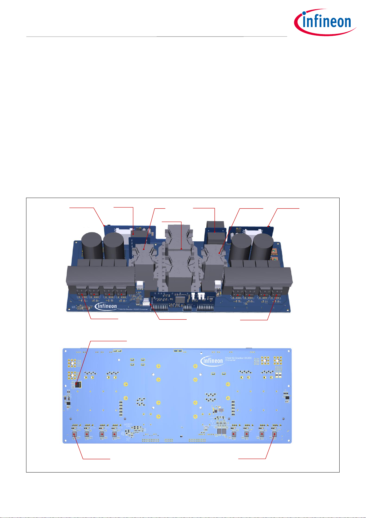
In UG-2020-31, Figure 1 shows the placement of the different components on the 11 kW bi-directional DC-DC
converter. The outer dimensions of the board, enclosed in the case, are 33.1 mm x 13.4 mm x 6 mm, which results
in a power density in the range of 4.1 W/cm³ (5.5 W/g).
Auxiliary Power Board
Auxiliary Power Board
1200 V SiC MOSFETs- IMZ120R030M1H
Controller Board
1200 V SiC MOSFETs- IMZ120R030M1H
Driver ICs-1EDC20I12AH
Driver ICs-1EDC20I12AH
Current Sensor- TLI4971
Resonant capacitor
Resonant Inductor
Resonant InductorResonant capacitor
Transformer
Page 6

6 of 37
2020-11-03
11 kW bi-directional CLLC DC-DC converter with 1200V and 1700V CoolSiC™
MOSFETs
The board at a glance
Figure 1 Placement of the different sections in the 11 kW bi-directional CLLC DC-DC converter with
Infineon CoolSiC™ MOSFETs.
1.1 Delivery content
The 11 kW bi-directional board is a CLLC DC-DC converter developed with Infineon power semiconductors as
well as Infineon drivers, current sensor, controllers, communication chip, security chip and memory chip. The
combination of these devices can provide customers with an optimized system solution. The Infineon devices
used in the implementation of the 11 kW bi-directional board include:
Main power board
1200 V CoolSiC
TM
MOSFETs discretes - IMZ120R030M1H
1200VSingle channel IGBT gate driver IC in wide body package -1EDC20I12AH
XENSIV™ - high-precision coreless current sensors for industrial applications- TLI4971
Auxilary power board
1700 V CoolSiC™ MOSFET discretes- IMBF170R1K0M1
PWM-QR (quasi resonant) flyback control ICs- ICE5QSAG
Controller board
32-bit XMC4000 industrial microcontroller ARM® Cortex®-M4 family- XMC4400-F100k512 BA
High speed CAN transceiver generation-TLE9251VSJ
OPTIGA™ TRUST M -SLS32AIA
Low voltage drop linear voltage regulators - IFX25001TFV33
256-Kbit (32K × 8) serial (SPI) F-RAM: FM25V02A from Cypress
More information concerning these devices is available on the Infineon website.
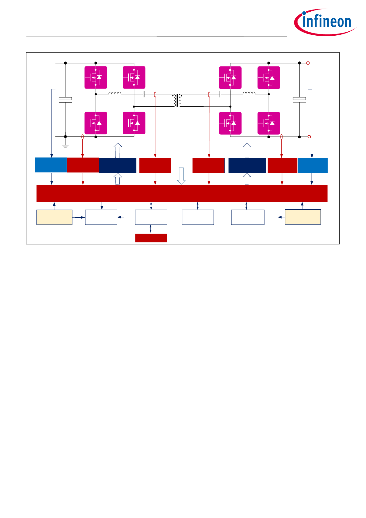
1.2 Block diagram
The REF-DAB11KIZSICSYS design consists of a CLLC in full-bridge configuration (Figure 2). The CLLC resonant
converter is widely used as a DC transformer to interlink the AC/DC to DC bus, because of its advantages of high
power density and the capacity of bi-directional power transfer. In both forward and reverse modes, the
resonant tank possesses almost the same operational characteristics of the conventional LLC resonant
tank.Thus the ZVS+ZCS soft switching can be achieved both in forward and reverse modes, and the switching
losses can be minimized, thereby improving charger efficiency.
This architecture showed in the block diagram contains three parts, the main power circuit, the auxiliary power
board and the control board.
Page 7
7 of 37
2020-11-03
11 kW bi-directional CLLC DC-DC converter with 1200V and 1700V CoolSiC™
MOSFETs
The board at a glance
Isolated gate driver
1EDC20I12AH
Isolated current
transformer
Isolated current
transformer
Isolated voltage
sensor
Isolated
voltage sensor
XMC4400 MCU Controller
Aux power
CoolSET+SIC MOS
FAN Wifi Module Cypress FeRAM OPTIGATrust X
NTC
Current sensor
isolated
Aux power
CoolSET+SIC MOS
Current sensor
TLI4971
Isolated gate driver
1EDC20I12AH
GUI
Figure 2 11 kW bi-directional CLLC DC-DC converter (REF-DAB11KIZSICSYS ) – simplified diagram
showing the Infineon semiconductors used in the system
The main power circuit includes 1200 V CoolSiCTM MOSFETs make high efficiency possible.
The auxiliary power supply uses 1700 V CoolSiCTM MOSFETs for an efficient design, as it is as small as a card.
The control is implemented in an XMC4400 Infineon microcontroller, which includes the following features:
ARM® Cortex™-M4, 120MHz, incl. single cycle DSP MAC and floating point unit (FPU)
8-channel DMA + dedicated DMAs for USB and Ethernet
USIC 4ch [Quad SPI, SCI/UART, I²C, I²S, LIN]
Supply voltage range: 3.13 - 3.63V
USB 2.0 full-speed, on-the-go
CPU frequency: 120MHz
Peripherals‘ clock: 120 [MHZ]
eFlash: 512 kB including hardware ECC
80 kB SRAM
10/100 Ethernet MAC (/w IEEE 1588)
2x CAN, 64 MO
Package: PG-LQFP-100
4x ΔΣ demodulator
Temperature range from -40° to 125°
Further details about the digital control implementation and other functionalities of CLLC in the XMC™ 4000
family can be found on the Infineon website.
Page 8
8 of 37
2020-11-03
11 kW bi-directional CLLC DC-DC converter with 1200V and 1700V CoolSiC™
MOSFETs
The board at a glance
1.3 Main features
A bi-directional full-bridge CLLC resonant converter using a symmetric CLLC-type resonant network
is proposed for a bi-directional power distribution system. This converter can operate under high
power conversion efficiency, as the symmetric LLC resonant network has zero-voltage switching
capability for primary power switches and sychronous rectification capability for secondary- side
rectifiers.
In addition, the proposed topology does not require any snubber circuits to reduce the voltage stress
of the switching devices because the switch voltage of the primary and secondary power stage is
confined by the input and output voltage, respectively. In addition, the power conversion efficiency
of any direction is similar. Intelligent digital-control algorithms are also proposed to regulate output
voltage, control bi-directional power conversions and to achieve synchronous rectification.
1.4 Board parameters and technical data
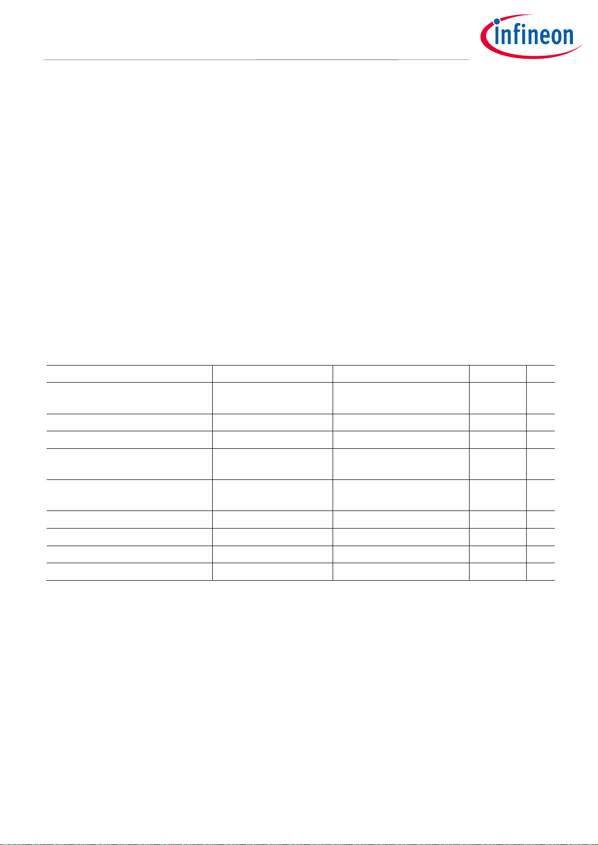
Table 2 shows the specifications of the board
Table 2 Parameter
Parameter
Symbol
Conditions
Value
Unit
Rated power P V
bus
=750V,
VHV=800V,Ta=250C. I
pri.
=15A
11
KW
Primay side bus voltage
V
bus
-
750
V
Secondary side bus voltage
VHV
-
550-~800
V
Primay side current
I
pri.
V
bus
=750V,
VHV=800V,Ta=250C. I
pri.
=15A
15
A
Secondary side current
I
sec.
VHV=550V,P=11KW,
Ta=250C.
20
A
Switching frequency
fs
-
40~200
Khz
Auxilary power output voltage
V
aux.
P
aux.
=32W
15/20
V
Auxilary power output power
P
aux.
V
aux.
=20V, ,Ta=250C.
32
W
Board net weight
W
Without encloser
2
Kg
Page 9
9 of 37
2020-11-03
11 kW bi-directional CLLC DC-DC converter with 1200V and 1700V CoolSiC™
MOSFETs
System and functional description
2 System and functional description
2.1 Commissioning
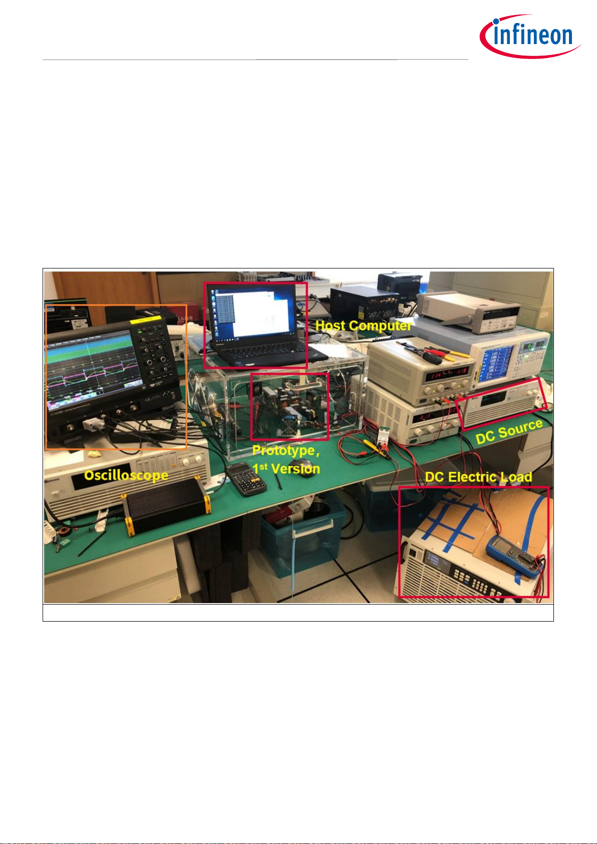
This chapter presents the set-up on how to evaluate the performance and behavior of the 11 kW bi-directional
DC-DC converter using CoolSiC™ MOSFETs.
DC source provides the power to the converter prototype
Secondary side of converter prototype connect with the DC electric load
The host computer controls the start and stop of the prototype and sets the working parameters
through GUI
Observe the corresponding waveforms with an oscilloscope
Figure 3 11 kW bi-directional CLLC DC-DC converter measuring environment
2.2 Description of the functional blocks
The 11 kW bi-directional CLLC DC-DC converter can operate as an isolated buck or as an isolated boost
converter, with the power flowing from the bus side to the isolated HV side or vice versa.
For validation of the buck mode, the suggested set-up includes:
Bus supply capable of 700 V~800 V and at least 11 kW (when testing up to full load)
HV electronic load (500 V to 800 V), in constant current mode, capable of at least 11 kW (when testing up to full
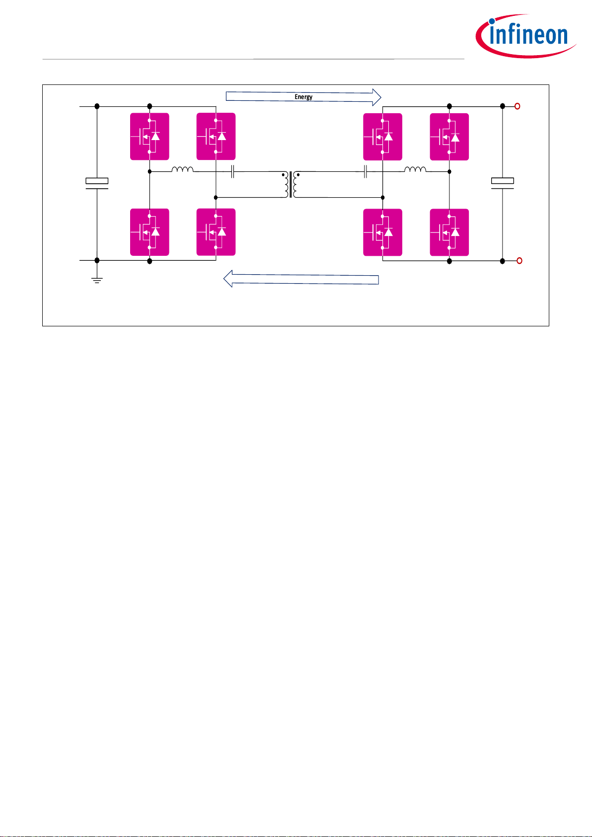
load). Nominal input voltage of the converter is 750 V. The converter works as indicated in Figure 4.
Page 10
10 of 37
2020-11-03
11 kW bi-directional CLLC DC-DC converter with 1200V and 1700V CoolSiC™
MOSFETs
System and functional description
Bus
HV
36uH 132nF 22uH216nF
20:16,Lm=160uH
Q1
Q2
Q3
Q4
Q5
Q6
Q7
Q8
Figure 4 Buck mode recommended validation set-up
For validation of the boost mode, the suggested set-up is exactly the same as for the buck mode, except for
thing: the output voltage parameter must be changed in the GUI window.
2.2.1 Description of the functional blocks
The output gain function of CLLC topology is generally analyzed by the fundamental wave-analysis method.
Based on this analysis method, the parameters of the key resonant components in the current design are
shown in the Figure 4:
By using this parameter, the resonance parameter Q of the primary and secondary transformers is consistent,
and the natural resonance frequency is 73 kHz. In the design, we chose a switching frequency of the topology in
the range of 40 kHz to 200 KHz.
The structure of CLLC topology on the primary side and the secondary side is the same. On the contrary, the
fundamental wave-analysis method is also valid. The relationship between the output/input gain and the
switching frequency of the circuit is shown in Error! Reference source not found.(reverse energy
transmission):
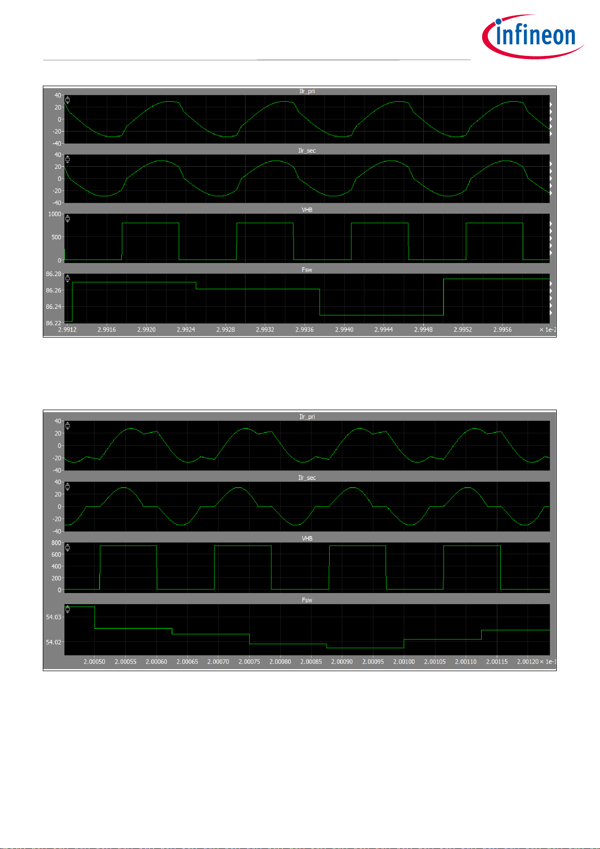
The current of the primary/secondary resonant cavity and the Vds waveform of the SiC MOSFET in the steady
state can be obtained as follows with the help of PLECS simulation software for verification:
Buck mode (forward-energy transmission), input voltage 800 V, and output voltage 550 V with load 27.5 Ω. At
this time, the CLLC topology switching frequency is 86.2 KHz:
Ilr_pri is the primary side resonant tank current.
Ilr_sec is the secondary side resonant tank current.
VHB is the V
ds
voltage of Q2 (The position of SiC MOSFETs Q1~Q8 can be seen in Figure 4.).
Fsw is the switching frequency.
Page 11
11 of 37
2020-11-03
11 kW bi-directional CLLC DC-DC converter with 1200V and 1700V CoolSiC™
MOSFETs
System and functional description
Figure 5 Simulation result of CLLC buck mode
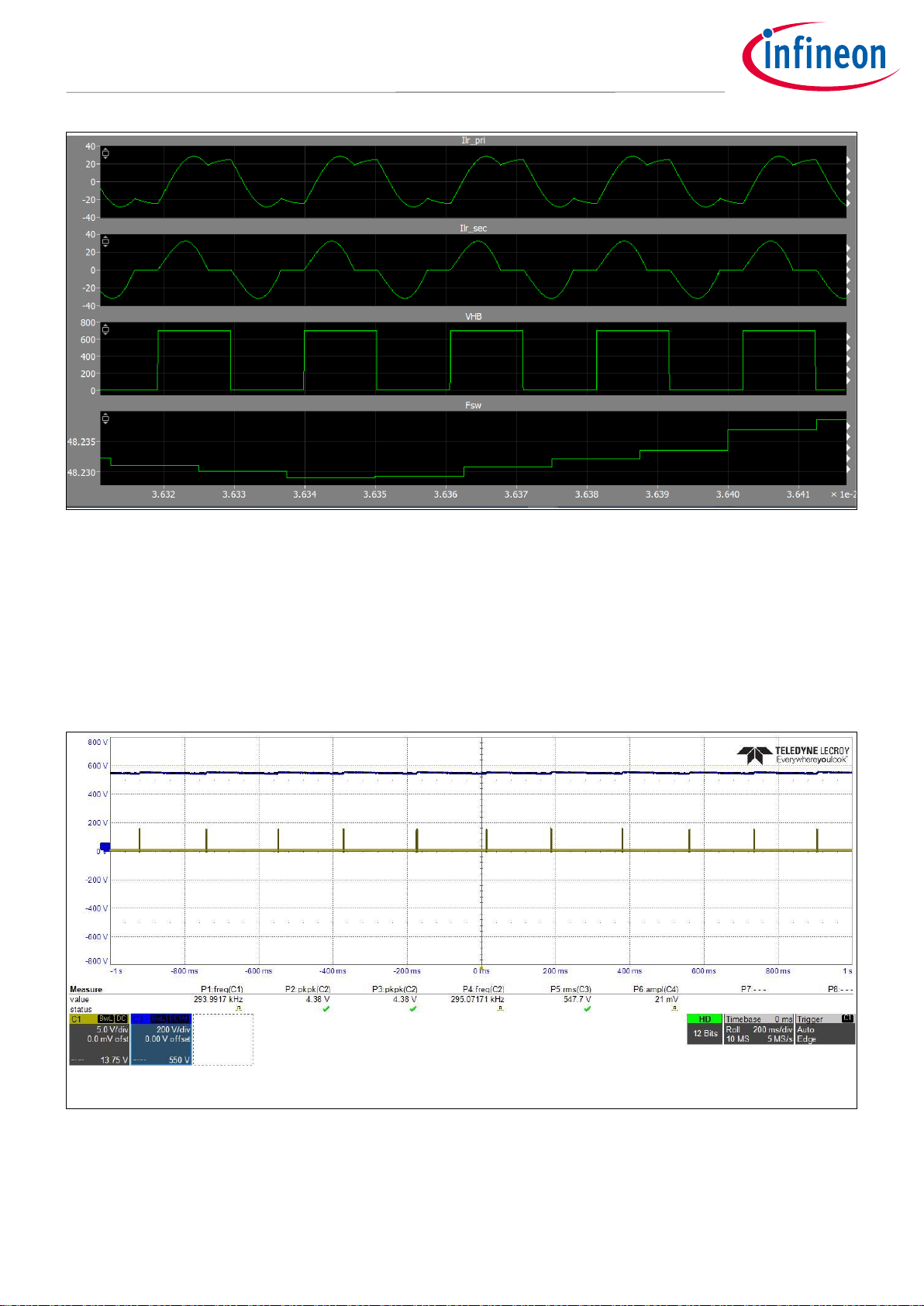
Forward-energy transmission, input voltage 750 V, output voltage 750 V, load 51.1 Ohm. The switching
frequency of CLLC topology is 54.0 KHz at this condition, the simulation wavefrom can be seen in Figure 6.
Figure 6 Simulation result of CLLC
Boost mode (forward-energy transmission), input voltage 700 V, output voltage 800 V, load 58.1 Ohm. At this
time, the CLLC topology switching frequency is around 48.2 KHz:
Page 12
12 of 37
2020-11-03
11 kW bi-directional CLLC DC-DC converter with 1200V and 1700V CoolSiC™
MOSFETs
System and functional description
Figure 7 Simulation result of CLLC boost mode
In the case of no load or light load, the CLLC topology must work in frequency-modulation mode (PFM),
otherwise the power devices in the circuit may work at a very high switching frequency. Due to the existence of
parasitic parameters, the output voltage cannot be reduced to the target value under the circumstances of
continuous wave mode. The topology will work in this mode:
Channel 1 is the controller board ouput pulse-width modulation (PWM) signal.
Channel 2 is the output voltage.
Figure 8 Test result of light load
In the “burst” state, the output voltage waveform is as follows when a sudden load is added:
Channel 3 is the output voltage.
Page 13

13 of 37
2020-11-03
11 kW bi-directional CLLC DC-DC converter with 1200V and 1700V CoolSiC™
MOSFETs
System and functional description
Channel 4 is the load current.
Figure 9 Test result of added sudden load
At this time, there is an obvious overshoot of resonant cavity current according to Figure 10. If the peak value is
more than 40 A, it will trigger the overcurrent protection:
Channel 2 is the gate PWM signal of Q2.
Channel 3 is the V
ds
voltage of Q2.
Channel 4 is the primary side resonant tank current.
Figure 10 Test result of added sudden load
Page 14

14 of 37
2020-11-03
11 kW bi-directional CLLC DC-DC converter with 1200V and 1700V CoolSiC™
MOSFETs
System and functional description
Steady state, the Vgs/Vds voltage waveform of SiC MOSFET and current waveform in the resonation tank can be
seen in Figure 11.
Figure 11 Test waveform when the load is 10KW
For more expanded waveform details, please see Figure 12 below.
Figure 12 Details of V
gs/Vds
In Figure 13, the output voltage ripple is around 16.5 V; here we have considered the peak-to-peak value.
Channel 1 is the controller output PWM signal.
Channel 2 is the output voltage, here we consider the peak-to-peak value.
Page 15

15 of 37
2020-11-03
11 kW bi-directional CLLC DC-DC converter with 1200V and 1700V CoolSiC™
MOSFETs
System and functional description
Figure 13 Output voltage ripple
2.2.2 Special operation modes
The CLLC circuit used CoolSiCTM MOSFETs in the primary and secondary sides, so under normal work conditions
when one side of the transformer is in the switching state, the other side works in the diode rectification mode.
As known, MOSFET body diodes have considerable conduction voltage drops. Fortunately, the channel of the
MOSFET has reverse-conduction capability with a much smaller conducting voltage drop than its body diode.
Therefore it is necessary to adopt the synchronous rectification method to reduce the conduction loss on the
rectifier side, and improve the conversion efficiency.
Here explain a basic principle of the synchronous rectification scheme:
Under normal circumstances, dedicated synchronous rectifier drive controllers are widely used to detect the Vds
of the rectifier tube, and to control the gate drive in time. However, we cannot use this method in bi-directional
Page 16

16 of 37
2020-11-03
11 kW bi-directional CLLC DC-DC converter with 1200V and 1700V CoolSiC™
MOSFETs
System and functional description
DC/DC converters. In this board, we adopted another low-cost method to achieve synchronous rectification
control:
By sampling the current on the secondary side of the transformer through the current transformer CT,
and converting the periodic positive and negative current sampling signal into a DC current via the
rectifier circuit, then sending it to the non-inverting input of the comparator;
The comparator compares the rectified current sampling signal with a fixed threshold V
ref
, which is set
to be slightly more than 0;
The output inversion signal of the comparator and the primary pulse-width modulation (PWM) signal
are subjected to the AND operation and then sent to the corresponding rectifier drive circuit as the
drive signal. This process can also be completed by the MCU.
Below is the implementation block diagram of the synchronous rectification function:
Gate
Driver
&
Gate
Driver
V
rec
V
ref
V
comp.out
V
gs
Q1
Q2
Q3
Q4
Q5
Q6
Q7
Q8
Figure 14 Synchronous rectification function
With this method, it is easy to achieve synchronous rectification. At present, the AND operation between the flip
signal output by the comparator and the primary PWM signal is carried out inside the MCU. The MCU recognizes
that the comparator outputs a high level, and triggers an external interrupt, which is combined with the current
cycle of the PWM wave-sending sequence in the interrupt service routine. The corresponding synchronous
rectification drive is issued, but there is a certain delay in the actual measurement software processing. The
actual measurement current delay is about 1 s, and software optimization is required to reduce this delay
time.
Channel 1 is the V
ref
.
Channel 2 is output signal of the comparator.
Channel 3 is secondary side gate PWM signal.
Channel 4 is primary side gate PWM signal.
Page 17

17 of 37
2020-11-03
11 kW bi-directional CLLC DC-DC converter with 1200V and 1700V CoolSiC™
MOSFETs
System and functional description
Figure 15 Synchronous rectification gate signal
2.3 Auxiliary power boards
2.3.1 The technical specification of auxiliary power boards
The reference board is intended to support customers designing an auxiliary power supply for three-phase
converters using the Infineon 1700 V CoolSiC™ MOSFET. Potential applications include solar inverters, energy
storage, EV chargers, UPS and motor drives. Table 2 lists the key board specifications.
Table 3 Technical specifications
Input voltage
300 VDC to 900 VDC
Output power
32 W
Topology
Single-ended flyback
Output voltage
15V
20 V
Tolerance 2%
2%
Output current 2 A
2 A
Frequency
65~130 kHz, QR mode
Derating of switches VDS
85% (1450 V)
Efficiency at full load
>85%
2.3.2 Auxiliary power board description
The auxiliary power boards was developed using the 1700 V CoolSiC™ MOSFET in a single-ended flyback topology
to provide auxiliary power for these DC-DC converters.
The board has 20V outputs with up to 32 W output power working in a wide input voltage range from 200 VDC to
850 VDC. Its potential applications are any power electronic system having a high input voltage DC link.
This user guide contains an overview of the reference board’s operation, product information and technical
details with measurement results. The board uses 1700 V CoolSiC™ MOSFET in a TO-263 7L surface-mounted
Page 18

18 of 37
2020-11-03
11 kW bi-directional CLLC DC-DC converter with 1200V and 1700V CoolSiC™
MOSFETs
System and functional description
device (SMD) package as the main switch, which is well suited for high input voltage DC link, with single-ended
flyback topology. With low R
DS(on)
, high efficiency and low device temperature rise can be achieved with this
board.
The controller works in quasi-resonant mode to help reduce EMI noise. This information can help customers
during their design-in phase, and for re-use of the reference design board for their own specific requirements.
Figure 16 Pictures of auxiliary power board
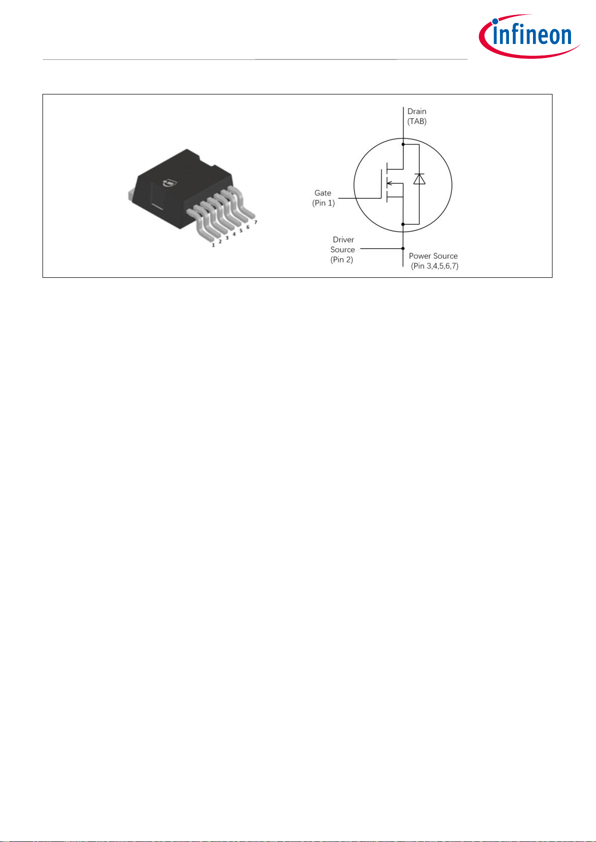
2.3.3 1700 V CoolSiC™ MOSFET overview
The auxiliary power board was developed using the 1700 V CoolSiC™ MOSFET in a single-ended flyback topology
to provide auxiliary power for this DC-DC. The 1700 V CoolSiC™ MOSFET from Infineon is an excellent choice for
high input voltage DC link systems like those found in auxiliary power supplies for three-phase converters. The
TO-263 7L surface-mounted device (SMD) package is an optimized package for up to 1700 V high voltage power
device. There is a creepage distance of about 7 mm width between drain and source, so safety standards are
easily met. The separate driver source pin is helpful in reducing parasitic inductance of the gate loop to prevent
gate-ringing effects.
Using Infineon’s 1700 V CoolSiC™ MOSFET can simplify the current auxiliary power supply designs by developing
a single-ended flyback reference design board. For a low-power auxiliary power supply, a flyback is the most
common topology due to its simple design. However, the flyback topology requires a switching device with a
high-blocking voltage. Currently, silicon MOSFETs only have a blocking voltage of up to 1500 V that leaves low
design margins, which affects the reliability of the power supply at a given input voltage DC link of 1000 VDC.
Moreover, most 1500 V silicon MOSFETs have very large on-state resistance (R
DS(on)
), which will lead to higher
losses, and thus lower system efficiency.
Page 19
19 of 37
2020-11-03
11 kW bi-directional CLLC DC-DC converter with 1200V and 1700V CoolSiC™
MOSFETs
System and functional description
Figure 17 1700 V CoolSiC™ MOSFET IMBF170R1K0M1
The ICE5QSAG gate drive output stage has a 0.9 A source capability, and output voltage up to 13 V, so the SiC
MOSFET can be driven directly, which simplifies the driver circuit design.
The auxiliary power board was developed using the 1700 V CoolSiC™ MOSFET in a single-ended flyback
topology to provide auxiliary power for this DC-DC. The 1700 V CoolSiC™ MOSFET from Infineon is an excellent
choice for high input voltage DC link.
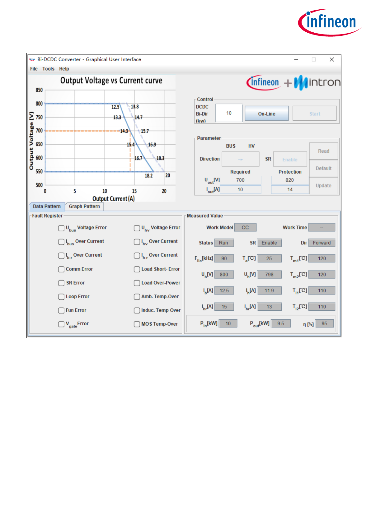
2.4 User interface
The 11 kW bi-directional DC-DC converter includes Wi-Fi wireless communication and the
corresponding protocol, allowing the converter system to implement the following functions through
the GUI interface of the computer:
System parameter setting (output direction, synchronous rectification function, output
voltage/current, voltage/current protection)
Working status control (connection, start/stop)
Running status display (measured value)
Abnormal status monitoring (fault register)
Abnormal analysis data reading (tools)
The signal chain between the GUI control interface and the converter system is the computer GUI
interface -> PC Wi-Fi connection -> DC-DC converter system.
The corresponding human-machine interface realizes corresponding functions through the
combination of graphics + data + buttons. The detailed interface is shown in the figure below:
Page 20
20 of 37
2020-11-03
11 kW bi-directional CLLC DC-DC converter with 1200V and 1700V CoolSiC™
MOSFETs
System and functional description
Figure 18 Graphical user interface (GUI)
There are two ways for the GUI to display real-time data:
Data dattern: Data parameter interface displays:
Working status, operating voltage/current, resonance parameters, temperature of key
components, abnormal status monitoring and display.
Page 21
21 of 37
2020-11-03
11 kW bi-directional CLLC DC-DC converter with 1200V and 1700V CoolSiC™
MOSFETs
System and functional description
Figure 19 Data pattern in GUI user
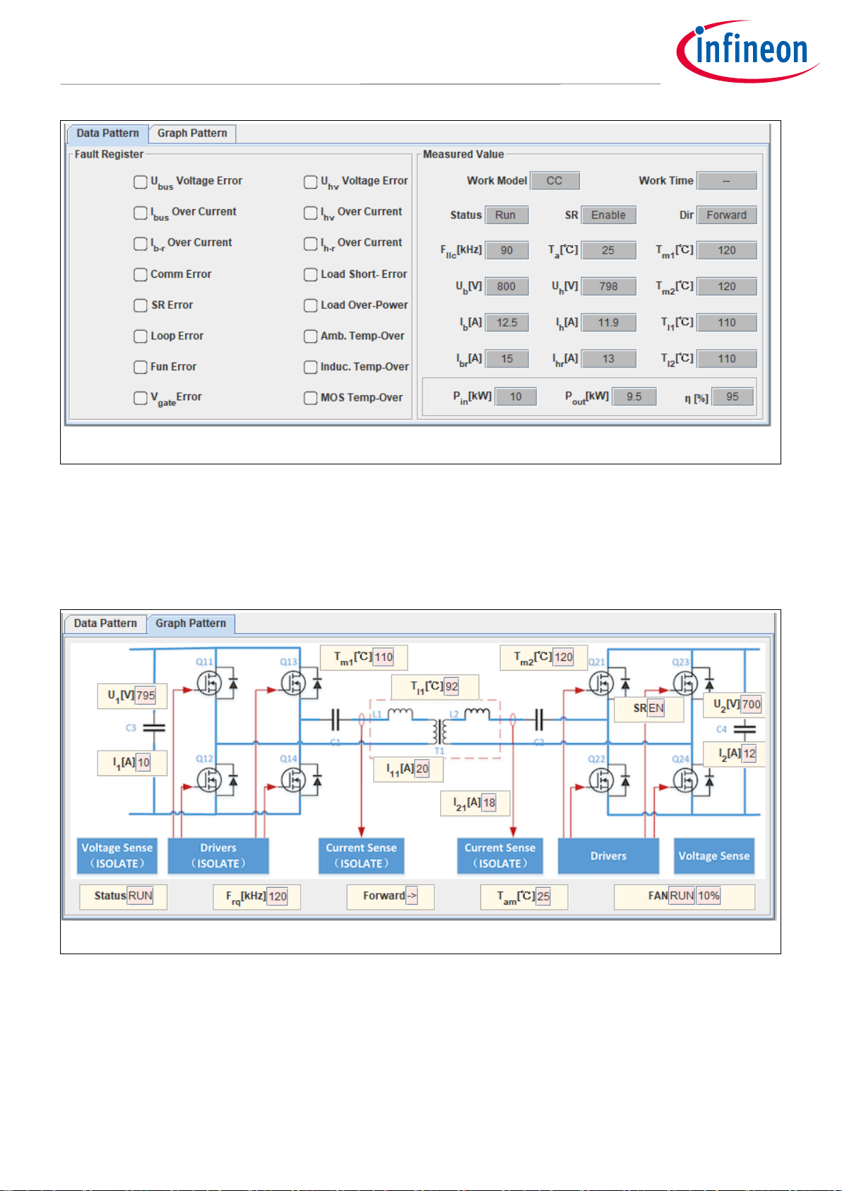
Graph Pattern:Graphical parameter interface displays:
Relevant real-time operating data of components in the corresponding position of topology of
the system.
Figure 20 Graph pattern in GUI user
Page 22

22 of 37
2020-11-03
11 kW bi-directional CLLC DC-DC converter with 1200V and 1700V CoolSiC™
MOSFETs
System design
3 System design
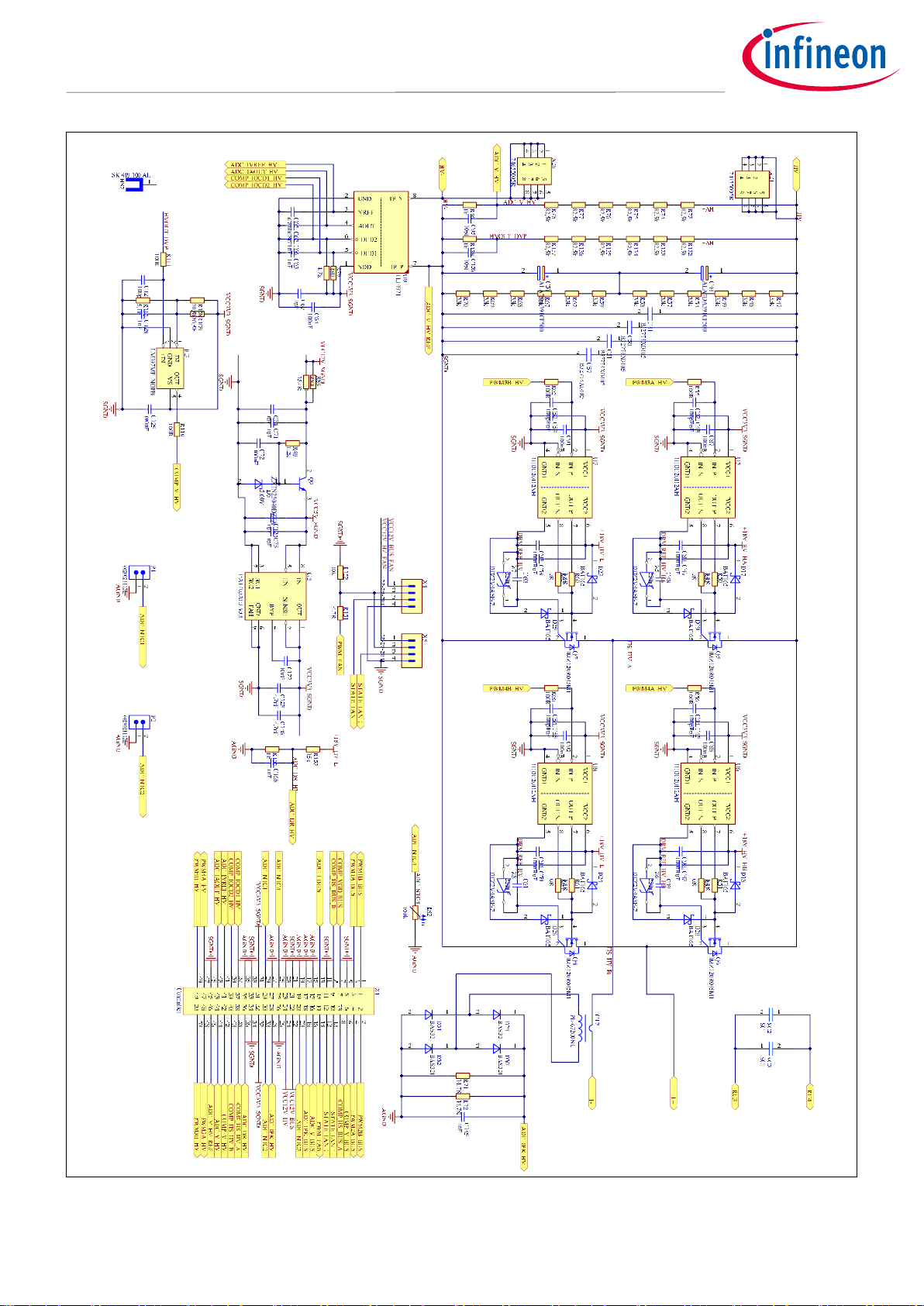
3.1 Schematics
Figure 21 Main board primary side schematic
Page 23
23 of 37
2020-11-03
11 kW bi-directional CLLC DC-DC converter with 1200V and 1700V CoolSiC™
MOSFETs
System design
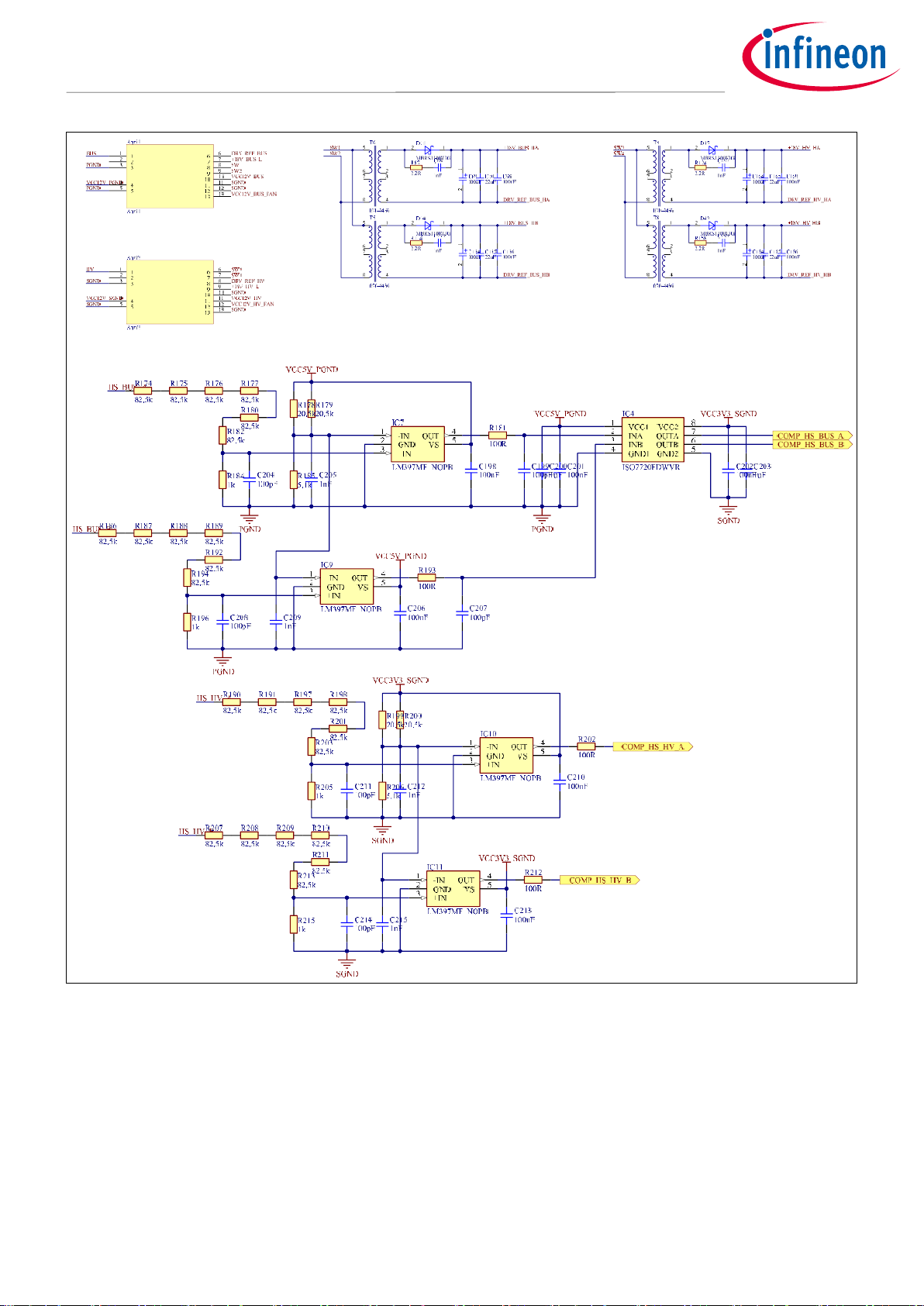
Figure 22 Main board secondary side schematic
Page 24

24 of 37
2020-11-03
11 kW bi-directional CLLC DC-DC converter with 1200V and 1700V CoolSiC™
MOSFETs
System design
Figure 23 32 W auxiliary power supply schematic.
Page 25
25 of 37
2020-11-03
11 kW bi-directional CLLC DC-DC converter with 1200V and 1700V CoolSiC™
MOSFETs
System design
Figure 24 Sensor circuit schematic
Page 26

26 of 37
2020-11-03
11 kW bi-directional CLLC DC-DC converter with 1200V and 1700V CoolSiC™
MOSFETs
System design
3.2 Layout
2111
13
14
16
17
18
19
20
1 1
9
8 7
6
543
2
1
9
8 7
6
543
2
1
9
8 7
6
543
2
1
9
8 7
6
543
2
1
13 12
1011 89 67 3 1245
1110987654321
1312
12
1 2
1 2
16
15
2
1
8
12
11
7
9
10
14
13
4
3
5
6
12
2
1
31
32
33
34
35
36
37
38
39
40
41
42
43
44
45
46
47
48
49
5030
29
28
27
26
25
24
23
22
211
2
3
4
5
6
7
8
9
10
11
12
13
14
15
16
17
18
19
20
12
1 2
1 2
2 1
1
2
1
2
1
2
2 1
1
2
12
1
2
1
2
1
2
12
1
2
1 2
3 4
1 2
3 4
1
2
3
4 5
6
7
8
1234
5 6 7 8
123
4 5
MH2MH1
12
MH2MH1
12
8765
1234
8765
1234
2
1
2
12
1
2
1
2
1
2
1
2
1
21
21
2
1
2
1
21
2
1
2
1
2
1 2
1
2
1
2
1
21
21
2 1
2
1
2 1
321 4 321 4321 4 321 4
321 4
321 4
321 4
321 4
21
2
1
21
1 2
21
21
21
2 1
2
1
2
1
2
1
2
1
1 2
1 2
1 2
1
2
1 2
2 1
12 2 1
4 3 2 1 4 3 2 1
2
1
2 1
1 2
2
1
1
2
1
2
4 3 2 1
5 6 7 8
8765
1234
2
1
1
2
2
1
1 2
21
1
2
2
1
1 2
21
1
2
1
2
1
2
1
2
Figure 25 Layer 1
Page 27

27 of 37
2020-11-03
11 kW bi-directional CLLC DC-DC converter with 1200V and 1700V CoolSiC™
MOSFETs
System design
2111
13
14
16
17
18
19
20
1 1
9
8 7
6
543
2
1
9
8 7
6
543
2
1
9
8 7
6
543
2
1
9
8 7
6
543
2
1
13 12
1011 89 67 3 1245
1110987654321
1312
12
1 2
1 2
16
15
2
1
8
12
11
7
9
10
14
13
4
3
5
6
31
32
33
34
35
36
37
38
39
40
41
42
43
44
45
46
47
48
49
5030
29
28
27
26
25
24
23
22
211
2
3
4
5
6
7
8
9
10
11
12
13
14
15
16
17
18
19
20
2 1
1
2
1
2
1
2
2 1
1
2
12
1
2
1
2
1
2
12
1
2
1 2
3 4
1 2
3 4
MH2MH1
12
MH2MH1
12
321 4 321 4321 4 321 4
321 4
321 4
321 4
321 4
4 3 2 1 4 3 2 1
Figure 26 Layer 2
Page 28

28 of 37
2020-11-03
11 kW bi-directional CLLC DC-DC converter with 1200V and 1700V CoolSiC™
MOSFETs
System design
2111
13
14
16
17
18
19
20
1 1
9
8 7
6
543
2
1
9
8 7
6
543
2
1
9
8 7
6
543
2
1
9
8 7
6
543
2
1
13 12
1011 89 67 3 1245
1110987654321
1312
12
1 2
1 2
16
15
2
1
8
12
11
7
9
10
14
13
4
3
5
6
31
32
33
34
35
36
37
38
39
40
41
42
43
44
45
46
47
48
49
5030
29
28
27
26
25
24
23
22
211
2
3
4
5
6
7
8
9
10
11
12
13
14
15
16
17
18
19
20
2 1
1
2
1
2
1
2
2 1
1
2
12
1
2
1
2
1
2
12
1
2
1 2
3 4
1 2
3 4
MH2MH1
12
MH2MH1
12
321 4 321 4321 4 321 4
321 4
321 4
321 4
321 4
4 3 2 1 4 3 2 1
Figure 27 Layer 3
Page 29

29 of 37
2020-11-03
11 kW bi-directional CLLC DC-DC converter with 1200V and 1700V CoolSiC™
MOSFETs
System design
2111
13
14
16
17
18
19
20
3
1
2
2
1
2
1
1
2
1
2
1
2
2
1
2
1
2 1
2 1
1
2
2
1
2 1
2
1
1 2
1 1
9
8 7
6
543
2
1
9
8 7
6
543
2
1
9
8 7
6
543
2
1
9
8 7
6
543
2
1
13 12
1011 89 67 3 1245
1110987654321
1312
12
1 2
1 2
16
15
2
1
8
12
11
7
9
10
14
13
4
3
5
6
1 2
2 1
21
31
32
33
34
35
36
37
38
39
40
41
42
43
44
45
46
47
48
49
5030
29
28
27
26
25
24
23
22
211
2
3
4
5
6
7
8
9
10
11
12
13
14
15
16
17
18
19
20
12
21
12
21
1 2
1 2
1 2
1 2
2
1
1 2
2 1
12
21
21
21
1 2
1 2
1 2
1 2
5 4
321
5 4
321
1
2
12
1
2
1
2
1 2
1
2
21
12
21
1 2
12
12
12
12
21
12
2 1
1 2
12
12
12
12
1 2 3
45
1 2 3
45
1 2 3 4
5678
2 1
21
2 1
2
1
2 1
21
21
21
2
1
2
1
21
2
1
2 1
1
2
1
2
1
2
2 1
1
2
12
1
2
1
2
1
2
12
1
2
1 2
3 4
1 2
3 4
1 2 3 4
5678
1 2 3
45
MH2MH1
12
MH2MH1
12
21
2
1
21
2
1
2
1
21
2
1
21
2
1
2
1
2
1
2
1
21
2
1
2
1
2
1
2
1
21
2
1
21
2
1
2
1
2
1
21
2
1
21
2
1
2
1
2
1
2 1
2 1
2
1
2 1
2 1
2
1
2
1
2
1
2
1
2
1
2
1
2
1
2
1
2
1
2
1
2
1
2
1
2
1
2
1
2
1
2
1
2
1
1 2
1
2
1
2
1
2
21
2 1
2 1
9
8765
4 3 2 1
321 4 321 4321 4 321 4
321 4
321 4
321 4
321 4
1 2
1 2
1 2
2
1
2
1
1
2
1
2
1 2
2 1 2 1
1 2
1 21 2
2
1
2
1
1 2
1
2
1
2
2 1 2 1
1 2
1 2
1 2
1 2
1
2
2
1
2
1
1
2
2
1
2
1
2
1
2
121
21
1 2
1 2
1 2
2
1
2
1
1
2
1
2
1 2
2 1
2 1
1 2
1 21 2
2
1
2
1
1 2
1
2
1
2
2 1
2 1
1 2
1 2
1 2
1 2
1
2
1
2
1
2
1
2
1
2
2
1
12
1
2
1
2
1
2
1
2
1
2
2 1
2
1
2
1
2
1
2
1
1 2
2
1
2 1
21
212 1
21
1234
5 6 7 8
1234
5 6 7 8
1234
5 6 7 8
1234
5 6 7 8
1234
5 6 7 8
1234
5 6 7 8
1234
5 6 7 8
1234
5 6 7 8
1
6
4 3 2 1 4 3 2 1
2
1
2
1
2
1
1
2
1 2
12
1234
5 6 7 8
9
5 4
321
2
1
2
1
1 2
12
2 1
1
2
21
1
2
2
1
1
2
2
1
2
1
Figure 28 Layer 4
Page 30

30 of 37
2020-11-03
11 kW bi-directional CLLC DC-DC converter with 1200V and 1700V CoolSiC™
MOSFETs
System design
3.3 Bill of material
The complete bill of material is available on the download section of the Infineon homepage. A log-in is
required to download this material.
Table 4 BOM of the most important/critical parts of the reference board
Comment
Description
Designator
Footprint
LibRef
Quantity
ALA7DA391CF500
Capacitor Polarised
C1, C17, C40,
C56
CAPPRD1000W210D3050H520
0
ALA7DA391CF500
4
B32774X0405
Capacitor
C2, C11, C12,
C18, C41, C50,
C51, C57
B32774X0405
B32774X0405
8
100pF
Surface Mount
Multilayer Ceramic
Chip Capacitor
C3, C5, C13,
C15, C25, C30,
C37, C42, C44,
C52, C54, C127,
C152, C153,
C157, C199,
C204, C207,
C208, C211,
C214, C244
CAPC1608X87N
245892
22
1uF
Surface Mount
Multilayer Ceramic
Chip Capacitor
(SMD MLCC)
C4, C6, C14,
C16, C24, C26,
C31, C34, C36,
C38, C43, C45,
C53, C55, C67,
C71, C74, C75,
C76, C124,
C151, C200,
C203
CAPC1608X87N
308640
23
1uF
Chip Monolithic
Ceramic Capacitor
C7, C8, C19,
C20, C46, C47,
C58, C59
CAPC2013X135N
310545
8
220nF
Multilayer Ceramic
Capacitor
C9, C10, C21,
C22, C48, C49,
C60, C61
CAPC2013X140N-1
491974
8
100nF
Surface Mount
Multilayer Ceramic
Chip Capacitor
C23, C27, C28,
C32, C33, C35,
C39, C64, C72,
C73, C80, C81,
C82, C83, C84,
C85, C86, C87,
C88, C89, C90,
C91, C92, C93,
C94, C98, C125,
C136, C169,
C186, C198,
C201, C202,
C206, C210,
C213, C242
CAPC1608X87N
251891
37
1nF
Surface Mount
Multilayer Ceramic
Chip Capacitor
C29, C63, C66,
C128, C145,
C158, C168,
C205, C209,
C212, C215,
C245, C246
CAPC1608X87N
246012, 239242
13
Page 31

31 of 37
2020-11-03
11 kW bi-directional CLLC DC-DC converter with 1200V and 1700V CoolSiC™
MOSFETs
System design
6.8nF
Chip Monolithic
Ceramic Capacitor
C62, C65
CAPC1608X90N
267248
2
1nF
SMD Comm C0G,
Ceramic Capacitor
C68, C133,
C162, C183
CAPC3216X88N
489640
4
100uF
Polymer Surface
Mount Chip
Capacitor Molded
Case, High
Performance Type
C69, C134,
C164, C184
CAPMP7343X310N-1
595120
4
22uF
Ceramic Chip
Capacitor, SMD,
MLCC,
Temperature
Stable
C70, C135,
C165, C185
CAPC3225X280N-2
308600
4
10pF
Capacitor, SMD,
MLCC, High
Temperature,
Ultra-Stable,
Automotive Grade
C95, C156
CAPC2013X88N
523442
2
10nF
Surface Mount
Multilayer Ceramic
Chip Capacitor
C122, C150
CAPC1608X09N
244517
2
4.7uF
High Value
Multilayer Ceramic
Capacitors (High
dielectric type)
C123, C126,
C146, C149
CAPC2113X140N
479052
4
PE-67200NL
Connector
CT1, CT2
PE67200NL
PE-67200NL
2
BAT165
Medium Power AF
Schottky Diode
D1, D2, D3, D4,
D7, D8, D9, D10,
D17, D18, D19,
D20, D23, D24,
D25, D26
SOD2513X110N
420071
16
5.60V
1.5 Watt Plastic
Surface Mount
Zener Voltage
Regulator
D5
DIOM5226X220N
513956
1
BAS321
General Purpose
Diode
D13, D14, D15,
D16, D29, D30,
D31, D32
SOD2513X110N-1
393569
8
MBRS1100T3G
Schottky Power
Rectifier
D21, D34, D37,
D43
DIOM5436X247N
519286
4
IFX1763XEJV50
Wide Input Range
Low Noise 500mA
5V LDO
G1
SOIC127P600X170-9N
424464
1
IFX1763XEJ V33
Wide Input Range
Low Noise 500mA
LDO
G2
SOIC127P600X170-9N
428662
1
SK 489 100 AL
Extruded Heatsink
for Lock-in
Retaining Spring,
PCB mounting,
100mm L X
29.44mm W X
45mm H, Raw
degreased
aluminum
HS1, HS2
HS SK 489 100
416826
2
AMC1302QDWVRQ
1
Integrated Circuit
IC1
SOIC127P1150X280-8N
AMC1302QDWVRQ
1
1
Page 32

32 of 37
2020-11-03
11 kW bi-directional CLLC DC-DC converter with 1200V and 1700V CoolSiC™
MOSFETs
System design
AMC1311QDWVQ1
Integrated Circuit
IC2
SOIC127P1150X280-8N
AMC1311QDWVQ1
1
LM397MF_NOPB
Integrated Circuit
IC3, IC6, IC7,
IC8, IC9, IC10,
IC11
SOT95P280X145-5N
LM397MF_NOPB
7
ISO7720FDWVR
Integrated Circuit
IC4, IC5
SOIC127P1150X280-8N
ISO7720FDWVR
2
66200211122
THT Male Header
WR-MPC3,
Vertical, Single
Row, pitch 3 mm, 2
pins
P1, P2
66200211122
66200211122
2
IMZ120R045M1
CoolSiC 1200 V SiC
Trench MOSFET
Q1, Q2, Q3, Q4,
Q5, Q6, Q7, Q8
INF-PG-TO247-4
498554
8
ZXTN25040DZTA
40V, SOT89, NPN
medium power
transistor, PD =
2.4W
Q9
SOT89
527905
1
33k
Standard Thick
Film Chip Resistor
R1, R2, R3, R8,
R11, R12, R13,
R16, R21, R22,
R23, R24, R47,
R48, R49, R54,
R57, R58, R59,
R62, R67, R68,
R69, R70
RESC3216X60N
354467
24
1.8R
General Purpose
Chip Resistor
R4, R5, R14,
R15, R50, R51,
R60, R61
RESC3116X65N
329186
8
0R
Standard Thick
Film Chip Resistor
R6, R7, R17,
R18, R52, R53,
R63, R64
RESC3216X60N
351892
8
100R
General Purpose
Chip Resistor
R9, R10, R19,
R20, R29, R31,
R38, R39, R44,
R55, R56, R65,
R66, R110,
R111, R147,
R181, R193,
R202, R212,
R217
RESC1608X55N-1
327766
21
3mR
High Power
Current Sense Chip
Resistor
R25, R28
RESC6432X90N
516046
2
22R
Standard Thick
Film Chip Resistor
R26, R27
RESC2113X50N
348647
2
1k
General Purpose
Chip Resistor
R30, R155, R218
RESC1608X55N-1
327826
3
110k
Standard Thick
Film Chip Resistor
R32, R33, R34,
R35, R36, R37
RESC3216X60N
354772
6
1.2k
General Purpose
Chip Resistor
R40
RESC1608X55N-1
327831
1
51.1R
Standard Thick
Film Chip Resistor
R41
RESC3216X60N
352877
1
57.6R
Standard Thick
Film Chip Resistor
R42, R43
RESC3216X60N
352907
2
1k
Thick Film Chip
Resistor
Automotive Grade
R45, R149,
R184, R196,
R205, R215
RESC2013X60N
331288
6
Page 33

33 of 37
2020-11-03
11 kW bi-directional CLLC DC-DC converter with 1200V and 1700V CoolSiC™
MOSFETs
System design
1k
Standard Thick
Film Chip Resistor
R46, R138
RESC3216X60N
353612
2
14.7R
Standard Thick
Film Chip Resistor
R71, R72
RESC2113X50N
348552
2
82.5k
Standard Thick
Film Chip Resistor
R73, R74, R75,
R76, R77, R78,
R132, R133,
R134, R135,
R136, R137,
R139, R140,
R141, R142,
R145, R146,
R174, R175,
R176, R177,
R180, R182,
R186, R187,
R188, R189,
R190, R191,
R192, R194,
R197, R198,
R201, R203,
R207, R208,
R209, R210,
R211, R213
RESC3216X60N
354707
42
4.7k
General Purpose
Chip Resistor
R79, R80
RESC1608X55N-1
327866
2
100k
Multilayer NTC
Thermistor
R81, R82
RESC1608X90N
494379
2
15.4R
Standard Thick
Film Chip Resistor
R83, R84
RESC3216X60N
352567
2
2.2R
Standard Thick
Film Chip Resistor
R87, R114,
R124, R158
RESC3216X60N
352082
4
15k
Standard Thick
Film Chip Resistor
R107, R153,
R216
RESC1609X50N
346262
3
20.5k
Standard Thick
Film Chip Resistor
R108, R109,
R143, R144,
R178, R179,
R199, R200
RESC1609X50N
346337
8
5.1k
Standard Thick
Film Chip Resistor
R112, R150,
R185, R206
RESC1609X50N
346002
4
4.7R
Standard Thick
Film Chip Resistor
R151
RESC2113X50N
348277
1
10k
General Purpose
Chip Resistor
R152
RESC2013X60N
328501
1
SC SC1, SC2, SC3
PCBComponent_1 - duplicate1
SC 3 TRANS
T1
PCBComponent_1
TRANS
1
070-4436
Transformer 8Terminal EXT,
SMD, Horizontal,
EP Style Bobbins,
EP7
T4, T5, T6, T8
EP7_4436
EP7, 070-4436
4
1EDC20I12AH
Single channel
IGBT gate driver IC
Up to 10 A typical
peak current , ±2.0
A Output current
configuration
U1, U2, U3, U4,
U5, U6, U7, U8
SOIC127P1030X265-8N-V
583333
8
Page 34

34 of 37
2020-11-03
11 kW bi-directional CLLC DC-DC converter with 1200V and 1700V CoolSiC™
MOSFETs
System design
TLI4971
High Precision
Coreless Current
Sensor
U9
INF-PG-TISON-8
431513
1
Controller
X1
PCBComponent_1 - duplicate3
Controller
1
74655095R
Connector
X3, X10, X21,
X26
74655095R
74655095R
4
22-29-2041
KK 254 Wire-toBoard Header,
Vertical, with
Friction Lock, 4
Pins
X4, X5
CON-M-THT-22-29-2041
383946
2
DDZ2V4ASF-7
Zener Diode
Z1, Z2, Z3, Z4,
Z5, Z6, Z7, Z8
SODFL2512X75N
DDZ2V4ASF-7
8
Page 35

35 of 37
2020-11-03
11 kW bi-directional CLLC DC-DC converter with 1200V and 1700V CoolSiC™
MOSFETs
References and appendices
4.1 Abbreviations and definitions
Table 5 Abbreviations
Abbreviation
Meaning
CE
Conformité Européenne
EMI
Electromagnetic interference
UL
Underwriters Laboratories
4.2 References
[1] “800 W ZVS phase-shift full-bridge evaluation board. Using 600 V CoolMOS™ CFD7 and digital control by
XMC4200”, AN_201709_PL52_027
[2] “1400 W ZVS phase-shift full-bridge evaluation board. Using 600 V CoolMOS™ CFD7 and digital control by
XMC4200”, AN_201711_PL52_003
[3] Jared Huntington, “6 W bias supply. Using the new 800 V CoolMOS™ P7, ICE5QSAG QR flyback controller,
and snubberless flyback for improved auxiliary power-supply efficiency and form factor”,
AN_201709_PL52_030
[4] Design of CLLC Resonant Converters for the Hybrid AC/DC Microgrid Applications
[5] IMBF170R1K0M1 datasheet, 1700 V CoolSiC™ MOSFET
[6] UCC28600 datasheet, 8-Pin Quasi-Resonant flyback Green-Mode Controller
[7] Gate resistor for power devices, Infineon Technologies, application note AN2015-06
4.3 Additional information
This user guide describes the first design version. In case of any future design changes, this document will be
updated accordingly.
Board hardware will available in ISAR from February 2021 onwards.
Page 36

36 of 37
2020-11-03
11 kW bi-directional CLLC DC-DC converter with 1200V and 1700V CoolSiC™
MOSFETs
Revision history
Revision history
Document
version
Date of release
Description of changes
1.0
2020-11-03
First version
Page 37

Trademarks
All referenced product or service names and trademarks are the property of their respective owners.
Edition 2020-11-03
UG-2020-31
Published by
Infineon Technologies AG
81726 Munich, Germany
© 2021 Infineon Technologies AG.
All Rights Reserved.
Do you have a question about this
document?
Email: erratum@infineon.com
Document reference
For further information on the product, technology,
delivery terms and conditions and prices please
contact your nearest Infineon Technologies office
(www.infineon.com).
WARNINGS
Due to technical requirements products may contain
dangerous substances. For information on the types
in question please contact your nearest Infineon
Technologies office.
Except as otherwise explicitly approved by Infineon
Technologies in a written document signed by
authorized representatives of Infineon
Technologies, Infineon Technologies’ products may
not be used in any applications where a failure of the
product or any consequences of the use thereof can
reasonably be expected to result in personal injury.
 Loading...