

Page 1

User Manual Please read the Important Notice and Warnings at the end of this document V2.1
www.infineon.com
TriBoard TC3X9 TH V2.0(1) and TriBoard TC3X9 V2.0 2017-11
TriBoard TC3X9
TriBoard Manual TC3X9
Hardware: TriBoard TC3X9 TH V2.0(1) and TriBoard TC3X9 V2.0
About this document
Scope and purpose
The User Manual provide information about using, configuration and connecting the TriBoard with Infineon
AURIX™ TC3X9 device. The manual provide information for different hardware types. There exist different
hardware with Through Hole socket (TriBoard TC3X9 TH) and soldered devices (TriBoard TC3X9). The schematic
is identically for the all boards if not other mentioned in chapter schematic. The placing on the boards is
identically, all components are on the same location. Only the routing is different (socket need more space and
has through hole). All figures are valid for each board if not differently mentioned.
Intended audience
Design, verfication, test and software engineers will use this document to get an understanding of the
functionality and connections of the TriBoard.
Page 2

User Manual TOC-2 V2.1
TriBoard TC3X9 TH V2.0(1) and TriBoard TC3X9 V2.0 2017-11
TriBoard Manual TC3X9
Hardware: TriBoard TC3X9 TH V2.0(1) and TriBoard TC3X9 V2.0
Table of Contents
About this document . . . . . . . . . . . . . . . . . . . . . . . . . . . . . . . . . . . . . . . . . . . . . . . . . . . . . . . . . . . . . . . . . Preface-1
Table of Contents . . . . . . . . . . . . . . . . . . . . . . . . . . . . . . . . . . . . . . . . . . . . . . . . . . . . . . . . . . . . . . . . . . . . . . . TOC-2
1 Introduction . . . . . . . . . . . . . . . . . . . . . . . . . . . . . . . . . . . . . . . . . . . . . . . . . . . . . . . . . . . . . . . . . . . . . . . . . . . . . . 1-1
2 Features . . . . . . . . . . . . . . . . . . . . . . . . . . . . . . . . . . . . . . . . . . . . . . . . . . . . . . . . . . . . . . . . . . . . . . . . . . . . . . . . . . 2-1
2.1 Summary of Features . . . . . . . . . . . . . . . . . . . . . . . . . . . . . . . . . . . . . . . . . . . . . . . . . . . . . . . . . . . . . . . . . . . . . . . 2-1
2.2 Block Diagram . . . . . . . . . . . . . . . . . . . . . . . . . . . . . . . . . . . . . . . . . . . . . . . . . . . . . . . . . . . . . . . . . . . . . . . . . . . . . 2-3
2.3 Placement . . . . . . . . . . . . . . . . . . . . . . . . . . . . . . . . . . . . . . . . . . . . . . . . . . . . . . . . . . . . . . . . . . . . . . . . . . . . . . . . . 2-4
3 TriBoard Information . . . . . . . . . . . . . . . . . . . . . . . . . . . . . . . . . . . . . . . . . . . . . . . . . . . . . . . . . . . . . . . . . . . . . . 3-1
3.1 Usable devices . . . . . . . . . . . . . . . . . . . . . . . . . . . . . . . . . . . . . . . . . . . . . . . . . . . . . . . . . . . . . . . . . . . . . . . . . . . . . 3-1
3.2 Differences between TC389 and TC399 . . . . . . . . . . . . . . . . . . . . . . . . . . . . . . . . . . . . . . . . . . . . . . . . . . . . . . . 3-1
3.3 Power Supply . . . . . . . . . . . . . . . . . . . . . . . . . . . . . . . . . . . . . . . . . . . . . . . . . . . . . . . . . . . . . . . . . . . . . . . . . . . . . . 3-1
3.3.1 Failsafe handling . . . . . . . . . . . . . . . . . . . . . . . . . . . . . . . . . . . . . . . . . . . . . . . . . . . . . . . . . . . . . . . . . . . . . . . . . 3-2
3.4 LEDs . . . . . . . . . . . . . . . . . . . . . . . . . . . . . . . . . . . . . . . . . . . . . . . . . . . . . . . . . . . . . . . . . . . . . . . . . . . . . . . . . . . . . . 3-2
3.5 Clock . . . . . . . . . . . . . . . . . . . . . . . . . . . . . . . . . . . . . . . . . . . . . . . . . . . . . . . . . . . . . . . . . . . . . . . . . . . . . . . . . . . . . . 3-3
3.6 External Memory (only with TC399) . . . . . . . . . . . . . . . . . . . . . . . . . . . . . . . . . . . . . . . . . . . . . . . . . . . . . . . . . . 3-3
3.6.1 External Flash (only with TC399) . . . . . . . . . . . . . . . . . . . . . . . . . . . . . . . . . . . . . . . . . . . . . . . . . . . . . . . . . . . 3-3
3.6.2 External SRAM (only with TC399) . . . . . . . . . . . . . . . . . . . . . . . . . . . . . . . . . . . . . . . . . . . . . . . . . . . . . . . . . . . 3-3
3.7 USB Connector . . . . . . . . . . . . . . . . . . . . . . . . . . . . . . . . . . . . . . . . . . . . . . . . . . . . . . . . . . . . . . . . . . . . . . . . . . . . . 3-3
3.7.1 Serial Connection to PC . . . . . . . . . . . . . . . . . . . . . . . . . . . . . . . . . . . . . . . . . . . . . . . . . . . . . . . . . . . . . . . . . . . 3-4
3.7.2 miniWiggler JDS . . . . . . . . . . . . . . . . . . . . . . . . . . . . . . . . . . . . . . . . . . . . . . . . . . . . . . . . . . . . . . . . . . . . . . . . . . 3-4
3.8 FlexRay™ (E-RAY) . . . . . . . . . . . . . . . . . . . . . . . . . . . . . . . . . . . . . . . . . . . . . . . . . . . . . . . . . . . . . . . . . . . . . . . . . . . 3-5
3.9 Serial Eeprom . . . . . . . . . . . . . . . . . . . . . . . . . . . . . . . . . . . . . . . . . . . . . . . . . . . . . . . . . . . . . . . . . . . . . . . . . . . . . . 3-5
3.10 MultiCAN . . . . . . . . . . . . . . . . . . . . . . . . . . . . . . . . . . . . . . . . . . . . . . . . . . . . . . . . . . . . . . . . . . . . . . . . . . . . . . . . . . 3-5
3.11 LIN . . . . . . . . . . . . . . . . . . . . . . . . . . . . . . . . . . . . . . . . . . . . . . . . . . . . . . . . . . . . . . . . . . . . . . . . . . . . . . . . . . . . . . . . 3-5
3.12 Ethernet . . . . . . . . . . . . . . . . . . . . . . . . . . . . . . . . . . . . . . . . . . . . . . . . . . . . . . . . . . . . . . . . . . . . . . . . . . . . . . . . . . . 3-6
3.13 HSCT (optional) . . . . . . . . . . . . . . . . . . . . . . . . . . . . . . . . . . . . . . . . . . . . . . . . . . . . . . . . . . . . . . . . . . . . . . . . . . . . 3-6
3.13.1 High speed with HSCT . . . . . . . . . . . . . . . . . . . . . . . . . . . . . . . . . . . . . . . . . . . . . . . . . . . . . . . . . . . . . . . . . . . . . 3-6
3.14 ADC . . . . . . . . . . . . . . . . . . . . . . . . . . . . . . . . . . . . . . . . . . . . . . . . . . . . . . . . . . . . . . . . . . . . . . . . . . . . . . . . . . . . . . . 3-7
3.15 Other peripherals . . . . . . . . . . . . . . . . . . . . . . . . . . . . . . . . . . . . . . . . . . . . . . . . . . . . . . . . . . . . . . . . . . . . . . . . . . 3-8
3.16 Toggle LED’s . . . . . . . . . . . . . . . . . . . . . . . . . . . . . . . . . . . . . . . . . . . . . . . . . . . . . . . . . . . . . . . . . . . . . . . . . . . . . . . 3-8
3.17 Buttons . . . . . . . . . . . . . . . . . . . . . . . . . . . . . . . . . . . . . . . . . . . . . . . . . . . . . . . . . . . . . . . . . . . . . . . . . . . . . . . . . . . 3-8
3.18 Debug System . . . . . . . . . . . . . . . . . . . . . . . . . . . . . . . . . . . . . . . . . . . . . . . . . . . . . . . . . . . . . . . . . . . . . . . . . . . . . 3-9
3.18.1 OCDS1 . . . . . . . . . . . . . . . . . . . . . . . . . . . . . . . . . . . . . . . . . . . . . . . . . . . . . . . . . . . . . . . . . . . . . . . . . . . . . . . . . . . 3-9
3.18.2 DAP . . . . . . . . . . . . . . . . . . . . . . . . . . . . . . . . . . . . . . . . . . . . . . . . . . . . . . . . . . . . . . . . . . . . . . . . . . . . . . . . . . . . . 3-9
3.18.3 DAPE (only Emulation Device) . . . . . . . . . . . . . . . . . . . . . . . . . . . . . . . . . . . . . . . . . . . . . . . . . . . . . . . . . . . . . . 3-9
3.18.4 DAP_SCR . . . . . . . . . . . . . . . . . . . . . . . . . . . . . . . . . . . . . . . . . . . . . . . . . . . . . . . . . . . . . . . . . . . . . . . . . . . . . . . . 3-9
3.18.5 High speed with DAP/DAPE . . . . . . . . . . . . . . . . . . . . . . . . . . . . . . . . . . . . . . . . . . . . . . . . . . . . . . . . . . . . . . . . 3-9
3.18.6 AGBT (optional) . . . . . . . . . . . . . . . . . . . . . . . . . . . . . . . . . . . . . . . . . . . . . . . . . . . . . . . . . . . . . . . . . . . . . . . . 3-11
3.18.7 ETK connector (optional) . . . . . . . . . . . . . . . . . . . . . . . . . . . . . . . . . . . . . . . . . . . . . . . . . . . . . . . . . . . . . . . . 3-11
3.18.8 EmW Power (optional) . . . . . . . . . . . . . . . . . . . . . . . . . . . . . . . . . . . . . . . . . . . . . . . . . . . . . . . . . . . . . . . . . . 3-11
4 TriBoard Configuration . . . . . . . . . . . . . . . . . . . . . . . . . . . . . . . . . . . . . . . . . . . . . . . . . . . . . . . . . . . . . . . . . . . . 4-1
4.1 HW Boot Configuration . . . . . . . . . . . . . . . . . . . . . . . . . . . . . . . . . . . . . . . . . . . . . . . . . . . . . . . . . . . . . . . . . . . . . 4-1
4.1.1 Default Pad State . . . . . . . . . . . . . . . . . . . . . . . . . . . . . . . . . . . . . . . . . . . . . . . . . . . . . . . . . . . . . . . . . . . . . . . . . 4-1
4.1.2 Bootmode . . . . . . . . . . . . . . . . . . . . . . . . . . . . . . . . . . . . . . . . . . . . . . . . . . . . . . . . . . . . . . . . . . . . . . . . . . . . . . . 4-1
4.2 Assembly Options . . . . . . . . . . . . . . . . . . . . . . . . . . . . . . . . . . . . . . . . . . . . . . . . . . . . . . . . . . . . . . . . . . . . . . . . . . 4-2
4.2.1 General optional resistors . . . . . . . . . . . . . . . . . . . . . . . . . . . . . . . . . . . . . . . . . . . . . . . . . . . . . . . . . . . . . . . . . 4-2
Table of Contents
Page 3

User Manual TOC-3 V2.1
TriBoard TC3X9 TH V2.0(1) and TriBoard TC3X9 V2.0 2017-11
TriBoard Manual TC3X9
Hardware: TriBoard TC3X9 TH V2.0(1) and TriBoard TC3X9 V2.0
Table of Contents
4.2.2 Resistors for peripherals . . . . . . . . . . . . . . . . . . . . . . . . . . . . . . . . . . . . . . . . . . . . . . . . . . . . . . . . . . . . . . . . . . 4-4
4.2.3 Resistors for memories . . . . . . . . . . . . . . . . . . . . . . . . . . . . . . . . . . . . . . . . . . . . . . . . . . . . . . . . . . . . . . . . . . . . 4-6
5 Signal (on board used) Description . . . . . . . . . . . . . . . . . . . . . . . . . . . . . . . . . . . . . . . . . . . . . . . . . . . . . . . . . . 5-1
5.1 Power Signals . . . . . . . . . . . . . . . . . . . . . . . . . . . . . . . . . . . . . . . . . . . . . . . . . . . . . . . . . . . . . . . . . . . . . . . . . . . . . . 5-1
5.2 Reset Signals . . . . . . . . . . . . . . . . . . . . . . . . . . . . . . . . . . . . . . . . . . . . . . . . . . . . . . . . . . . . . . . . . . . . . . . . . . . . . . 5-1
5.3 Config Signals . . . . . . . . . . . . . . . . . . . . . . . . . . . . . . . . . . . . . . . . . . . . . . . . . . . . . . . . . . . . . . . . . . . . . . . . . . . . . . 5-2
5.4 Clock Signals . . . . . . . . . . . . . . . . . . . . . . . . . . . . . . . . . . . . . . . . . . . . . . . . . . . . . . . . . . . . . . . . . . . . . . . . . . . . . . 5-2
5.5 Debug Signals . . . . . . . . . . . . . . . . . . . . . . . . . . . . . . . . . . . . . . . . . . . . . . . . . . . . . . . . . . . . . . . . . . . . . . . . . . . . . . 5-2
5.6 Peripheral Signals . . . . . . . . . . . . . . . . . . . . . . . . . . . . . . . . . . . . . . . . . . . . . . . . . . . . . . . . . . . . . . . . . . . . . . . . . . 5-3
5.7 EBU Signals . . . . . . . . . . . . . . . . . . . . . . . . . . . . . . . . . . . . . . . . . . . . . . . . . . . . . . . . . . . . . . . . . . . . . . . . . . . . . . . . 5-4
6 Connector Pin Assignment . . . . . . . . . . . . . . . . . . . . . . . . . . . . . . . . . . . . . . . . . . . . . . . . . . . . . . . . . . . . . . . . . 6-1
6.1 On Board only used signals . . . . . . . . . . . . . . . . . . . . . . . . . . . . . . . . . . . . . . . . . . . . . . . . . . . . . . . . . . . . . . . . . . 6-1
6.2 TC3X9 Connector / Top View . . . . . . . . . . . . . . . . . . . . . . . . . . . . . . . . . . . . . . . . . . . . . . . . . . . . . . . . . . . . . . . . . 6-2
6.3 Power connector pinout . . . . . . . . . . . . . . . . . . . . . . . . . . . . . . . . . . . . . . . . . . . . . . . . . . . . . . . . . . . . . . . . . . . . 6-5
6.4 USB connector pinout . . . . . . . . . . . . . . . . . . . . . . . . . . . . . . . . . . . . . . . . . . . . . . . . . . . . . . . . . . . . . . . . . . . . . . 6-5
6.5 FlexRay™ (ERAY) connector pinout . . . . . . . . . . . . . . . . . . . . . . . . . . . . . . . . . . . . . . . . . . . . . . . . . . . . . . . . . . . 6-5
6.6 CAN connector pinout . . . . . . . . . . . . . . . . . . . . . . . . . . . . . . . . . . . . . . . . . . . . . . . . . . . . . . . . . . . . . . . . . . . . . . 6-5
6.7 LIN connector pinout . . . . . . . . . . . . . . . . . . . . . . . . . . . . . . . . . . . . . . . . . . . . . . . . . . . . . . . . . . . . . . . . . . . . . . . 6-6
6.8 HSCT connector pinout . . . . . . . . . . . . . . . . . . . . . . . . . . . . . . . . . . . . . . . . . . . . . . . . . . . . . . . . . . . . . . . . . . . . . 6-6
6.9 Ethernet connector pinout . . . . . . . . . . . . . . . . . . . . . . . . . . . . . . . . . . . . . . . . . . . . . . . . . . . . . . . . . . . . . . . . . . 6-6
6.10 OCDS1 connector pinout . . . . . . . . . . . . . . . . . . . . . . . . . . . . . . . . . . . . . . . . . . . . . . . . . . . . . . . . . . . . . . . . . . . . 6-7
6.11 DAP connector pinout . . . . . . . . . . . . . . . . . . . . . . . . . . . . . . . . . . . . . . . . . . . . . . . . . . . . . . . . . . . . . . . . . . . . . . 6-7
6.12 ETK connector pinout . . . . . . . . . . . . . . . . . . . . . . . . . . . . . . . . . . . . . . . . . . . . . . . . . . . . . . . . . . . . . . . . . . . . . . . 6-8
6.13 Ethernet miniWiggler power connector pinout . . . . . . . . . . . . . . . . . . . . . . . . . . . . . . . . . . . . . . . . . . . . . . . . 6-8
6.14 AGBT connector pinout . . . . . . . . . . . . . . . . . . . . . . . . . . . . . . . . . . . . . . . . . . . . . . . . . . . . . . . . . . . . . . . . . . . . . 6-9
7 Schematic and Layout . . . . . . . . . . . . . . . . . . . . . . . . . . . . . . . . . . . . . . . . . . . . . . . . . . . . . . . . . . . . . . . . . . . . . 7-1
7.1 Known problems . . . . . . . . . . . . . . . . . . . . . . . . . . . . . . . . . . . . . . . . . . . . . . . . . . . . . . . . . . . . . . . . . . . . . . . . . . . 7-1
7.1.1 Known problems (TriBoard TC3X9 TH V2.0(1)) . . . . . . . . . . . . . . . . . . . . . . . . . . . . . . . . . . . . . . . . . . . . . . . 7-1
7.1.2 Known problems (TriBoard TC3X9 V2.0) . . . . . . . . . . . . . . . . . . . . . . . . . . . . . . . . . . . . . . . . . . . . . . . . . . . . . 7-1
7.2 Schematic . . . . . . . . . . . . . . . . . . . . . . . . . . . . . . . . . . . . . . . . . . . . . . . . . . . . . . . . . . . . . . . . . . . . . . . . . . . . . . . . . 7-1
7.3 Layout . . . . . . . . . . . . . . . . . . . . . . . . . . . . . . . . . . . . . . . . . . . . . . . . . . . . . . . . . . . . . . . . . . . . . . . . . . . . . . . . . . 7-10
7.4 Layout with Dimensioning . . . . . . . . . . . . . . . . . . . . . . . . . . . . . . . . . . . . . . . . . . . . . . . . . . . . . . . . . . . . . . . . . 7-12
Page 4

User Manual 1-1 V2.1
TriBoard TC3X9 TH V2.0(1) and TriBoard TC3X9 V2.0 2017-11
TriBoard Manual TC3X9
Hardware: TriBoard TC3X9 TH V2.0(1) and TriBoard TC3X9 V2.0
Introduction
1Introduction
We congratulate you on your purchase of the TriCore Evaluation Board. This kit is a versatile tool, providing quick
access to the capabilities of TriCore's powerful architecture.
Applications can be developed easily. The Evaluation Board is equipped with a variety of memories and
peripherals for connection to the environment. There is also an interface for the On Chip Debugging Features
(OCDS1 and DAP).
The Evaluation Board allows easily the development of TriCore applications with the corresponding tools.
Subsequently, the applications can be downloaded and can be tested with the powerful debugger software.
This TriBoard Hardware Manual familiarizes you with the TriCore Evaluation Board and guides you through the
initial configuration of the TriBoard.
For detailed technical information about the TC3X9 (e.g. TC399, TC389) please refer to the User Manual of the
used device.
Page 5

User Manual 2-1 V2.1
TriBoard TC3X9 TH V2.0(1) and TriBoard TC3X9 V2.0 2017-11
TriBoard Manual TC3X9
Hardware: TriBoard TC3X9 TH V2.0(1) and TriBoard TC3X9 V2.0
Features
2Features
2.1 Summary of Features
– Infineon’s TC3X9 (TC399, TC389) AURIX™ 2G Controller in LFBGA-516 Package
– Infineon’s TC3X7 (TC397, TC387) AURIX™ 2G Controller in LFBGA-292 Package
– Burst Flash up to 4MBytes (only with TC399)
– asynchronous SRAM up to 2MByte (only with TC399)
– synchronous SRAM up to 4MByte (only with TC399)
–FlexRay™
1)
Transceivers
– High Speed CAN Transceivers (CAN-FD capable)
– USB to UART bridge
– Ethernet Gigabit PHY
–Serial Eeprom
–LIN Transceiver
– Crystal 20MHz (default) or External Clock
– USB miniWiggler JDS for easy debugging
– 8 Low Power Status LEDs
– 8-DIP switches for configuration
– access to all pins of controller
– 100mm x 160mm (EURO-Board)
Connectors
The TC3X9 TriBoard offers a wide variety of connectors:
– Standard power connector
– Micro USB connector for ASC Interface (ASC0) and miniWiggler
– RJ45 connector for Ethernet (10/100/1000)
– 16-pin header for JTAG interface (OCDS)
– 3 x 10-pin header for DAP, DAPE and DAP_SCR (DAPE only usable on Emulation Device)
– 10pin (2x5) Header for LIN Transceiver (LIN)
– 2 x 10pin (2x5) Header for CAN High Speed Transceiver (CAN0 and CAN1)
– 2 x 10pin (2x5) Header for FlexRay™ (ERAY-A and ERAY-B)
– five 80-pin connectors (male) + five 80-pin connectors (female) with all I/O signals
– optional ETK connector
– optional 2 x 6pin (IEEE1394) Socket for HSCT
– optional Aurora connector (only with Emulation Device)
Components
– Infineon’s Multi Voltage Safety Micro Processor Supply TLF35584QV
– Three LEDs to validate power supply (5Volt / 3,3 Volt / 1,25 Volt)
– LED indicating safe state signal 2 from TLF35584
– LED indicating /HDRST (ESR0) active state
– LED indicating activ miniWiggler JDS
– LED switched via DAS software
– 2 x Infineon’s FlexRay™ Transceiver TLE9221SX
– 2 x Infineon’s High Speed CAN-Transceiver TLE9251VSJ
1) FlexRay™ is a trademark of FlexRay Consortium.
Page 6

User Manual 2-2 V2.1
TriBoard TC3X9 TH V2.0(1) and TriBoard TC3X9 V2.0 2017-11
TriBoard Manual TC3X9
Hardware: TriBoard TC3X9 TH V2.0(1) and TriBoard TC3X9 V2.0
Features
– Infineon’s LIN-Transceiver TLE 7259-3GE
– USB to UART bridge FT2232HL (FTDI)
– Integrated 10/100/1000M Ethernet Precision Transceiver RTL8211FI-CG (Realtek)
– 8 general purpose LEDs
–2K I2C Serial Eeprom with EUI-48™
1)
Node Identity (MICROCHIP)
–Reset switch
–Enable switch
– Generic switch
– 4-pin Dip switch
Zero Ohm Bridges
Zero Ohm resistors give the flexibility to configure the systems functionality.
1) EUI-48™ is trademarked by IEEE
Page 7
User Manual 2-3 V2.1
TriBoard TC3X9 TH V2.0(1) and TriBoard TC3X9 V2.0 2017-11
TriBoard Manual TC3X9
Hardware: TriBoard TC3X9 TH V2.0(1) and TriBoard TC3X9 V2.0
Features
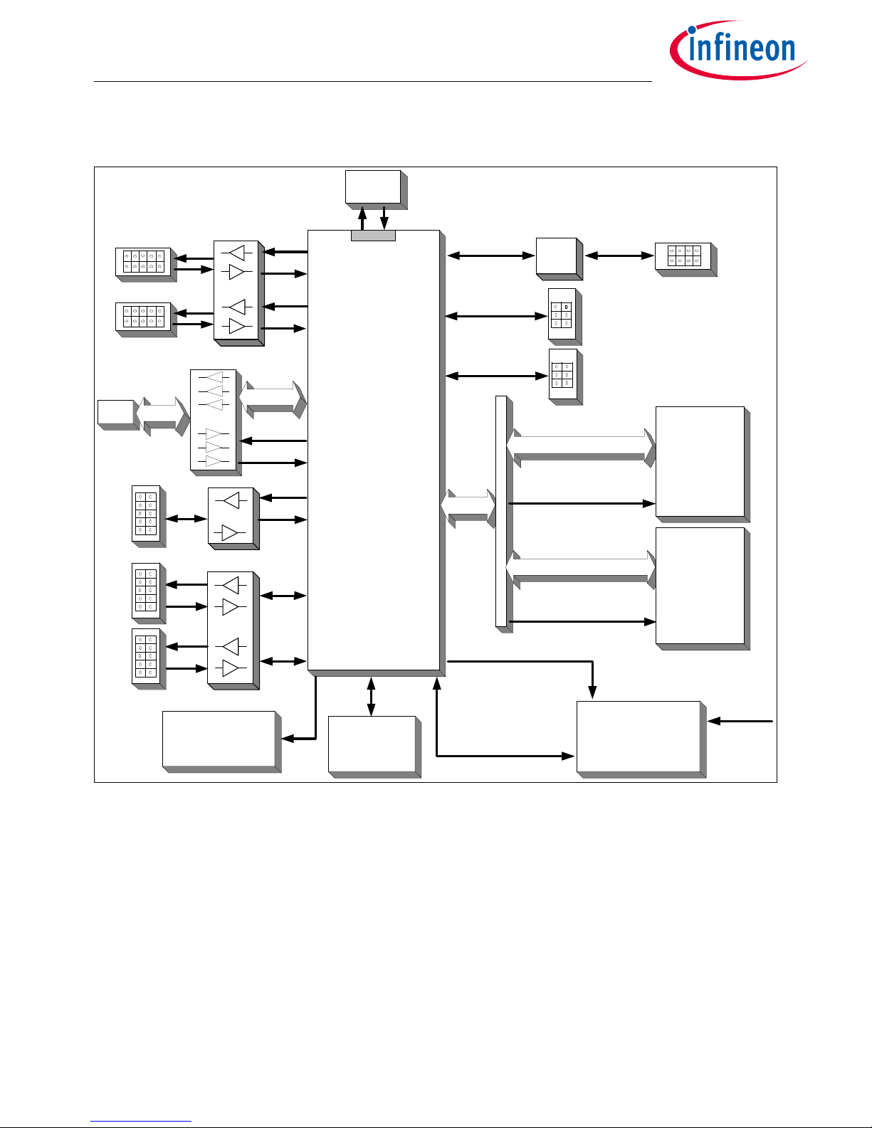
2.2 Block Diagram
Figure 2-1 TriBoard Block Schematic
Micro
USB
miniWiggler
OCDS1
USB
XTAL
FlexRay™
Tran sceive r
Transceiver
TxCAN0
TxCAN1
RxCAN0
RxCAN1
TC3X9
(e.g.
TC399,
TC389)
TriCore
CPU
PLL
CAN0
CAN1
ERAY B ERAY A
TX0
RX0
8 LED’s
(P33.4 up to P33.7,
P20.11 up to P20.14)
Seria l EEPROM
with EUI-48™
RGMII
PHY
Twisted Pair
RJ45
LIN
LIN
Tran sceive r
TX1
RX1
HSCT1
optional
HSCT1 - TX/RX
/CS0 or / CS1
/CS0 or /CS1
BUS
ADDRESS and DATA BUS
BUS
BUS
SRAM
32 Bit
Burst
FLASH
32 Bit
I²C
WAKEUP
QSPI2
Multi Voltage Safety Micro
Processor Supply
TLF35584QV
ENA
HSCT0 - TX/RX
HSCT0
optional
ONLY TC399
ONLY TC399
ONLY TC399
Page 8
User Manual 2-4 V2.1
TriBoard TC3X9 TH V2.0(1) and TriBoard TC3X9 V2.0 2017-11
TriBoard Manual TC3X9
Hardware: TriBoard TC3X9 TH V2.0(1) and TriBoard TC3X9 V2.0
Features
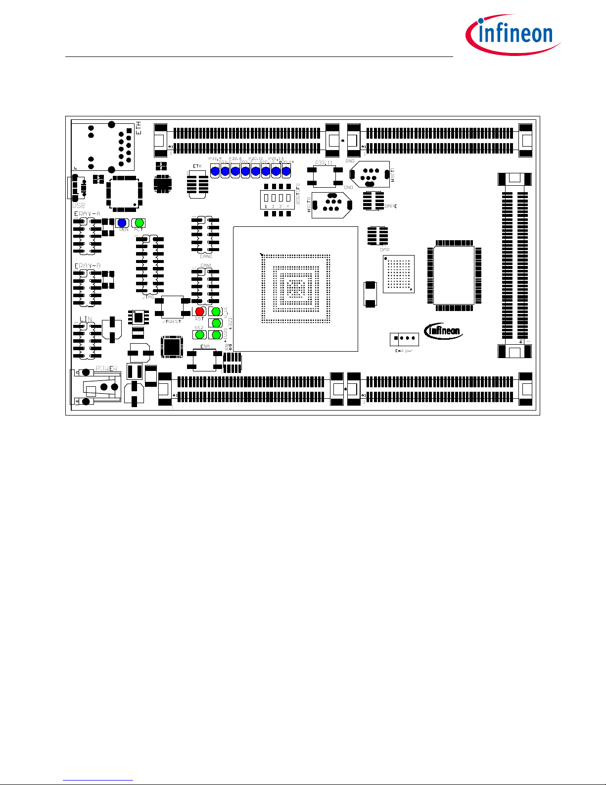
2.3 Placement
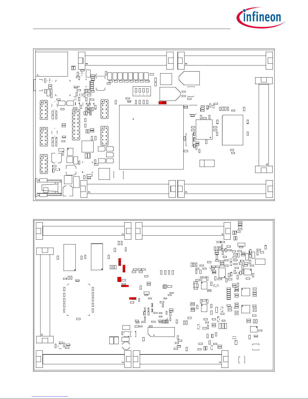
Figure 2-2
TriBoard TC3X9 (TH) V2.0(1) Placement
S202
D302 D303 D304 D305 D306 D307 D308 D309
Y201
X705
X702
X701X704
X703
X501
C501
U502
U501
L502
L501
C502
R501
S501
C303
X305
D506
X202
X406
S502
D508
X502
U604
U603
X40 4
X401
D504 D507
D505
X302 X301
T302
T301
X402
Y401
U401
D402
BU401
D401
X303X304
X30 6
X201
S201
X403
U201
U307
Y30 1
TriBoard-TC3X 9 (TH) V2.0(1)
Page 9

User Manual 3-1 V2.1
TriBoard TC3X9 TH V2.0(1) and TriBoard TC3X9 V2.0 2017-11
TriBoard Manual TC3X9
Hardware: TriBoard TC3X9 TH V2.0(1) and TriBoard TC3X9 V2.0
TriBoard Information
3 TriBoard Information
3.1 Usable devices
The board can be used with the following devices:
– TC399 A-Step (Ethernet and seond HSCT will not work in this case because device don’t support RGMII and
don’t have second HSCT)
–TC399 B-Step
– TC397 A-Step (Ethernet will not work in this case because device don’t support RGMII, external flash and
sram not usable)
– TC397 B-Step (external flash and sram not usable)
– TC389 A-Step (only if external flash and sram not assembled)
– TC387 A-Step (external flash and sram not usable)
Note: TC3X7 can be used with the innerballs (center) of BGA516, in this case all signals on the external 2
rows/colums are not connected/used.
Note: Please check always the latest manual for complete list of usable devices.
3.2 Differences between TC389 and TC399
Main difference between TC389 and TC399 is that the TC389 don’t had an external bus unit (EBU). Also the
corresponding VEBU pins of TC399 are connected to VEXT on TC389. Therefore you can’t use a TC389 in a board
assembled for TC399. The soldered boards always will have the correct assembling. For TriBoard TC3X9 TH
(socket variante) use with care.
Note: If the board has assembled external flash and sram then this
socket board can be used only with TC399. Don’t use this board
with TC389, this can be damaged the device and the board. If
there is no external flash and sram assembled then this socket
board can be used with TC399 and with TC389.
3.3 Power Supply
All needed voltages are generated via Infineon’s Multi Voltage Safety Micro Processor Supply TLF35584QV and via
the microcontroller itself (+1,25V).
The supply device is available as two different devices:
TLF35584QVVS1 -> +5V standby voltage, +5V TriCore supply (V_UC)
TLF35584QVVS2 -> +3,3V standby voltage, +3,3V TriCore supply (V_UC)
Dependent of the assembled device the board works with 5V or 3,3V IO.
The TLF35584QV provide the following voltages:
+3,3V or +5V for standby (connected to VEVRSB)
+3,3V or +5V for TriCore (connected to VEXT)
+5V communcation supply (used by CAN and FlexRay™ transceivers)
+5V voltage reference (connected to VDDM and VAREFx)
Page 10
User Manual 3-2 V2.1
TriBoard TC3X9 TH V2.0(1) and TriBoard TC3X9 V2.0 2017-11
TriBoard Manual TC3X9
Hardware: TriBoard TC3X9 TH V2.0(1) and TriBoard TC3X9 V2.0
TriBoard Information
+3,3V via LDO directly from pre regulator (used by Ethernet PHY and on board memories if assembled)
Applying a stable supply voltage causes the power on reset after a short period. The three LED's (V_UC, +3.3V,
+1V25) indicate the status of the on board generated voltages.
A manual power on reset is executed by pressing the reset button.
The Board has to be connected to a +3,5V to +40V DC power supply.
The power consumption is not specified yet but a supply with 12V and more than 500mA is recommended. The
pinout for the supply connector is shown in Figure 6-4. There can be used any standard power pack with a
connector where the positive line is surrounded by the ground line.
3.3.1 Failsafe handling
In case that the device don’t contains a program which disable or service the window watchdog and error pin
monitor of the TLF35584 then the TLF35584 is going to a FAILSAFE state where all supplies are switched off. This
state can be left via reconnect the power plug or via the ENA button (S502). In this case you must connect a
debugger which is able to disable the window watchdog and error pin monitor to reprogram the microcontroller.
In the default state of the board the switching to FAILSAFE state is switched off via resistor R508.
If you will use/evaluate all safety features of the TLF35584 remove assembled R508. Make sure that you have a
proper initialization of TLF35584 in your software.
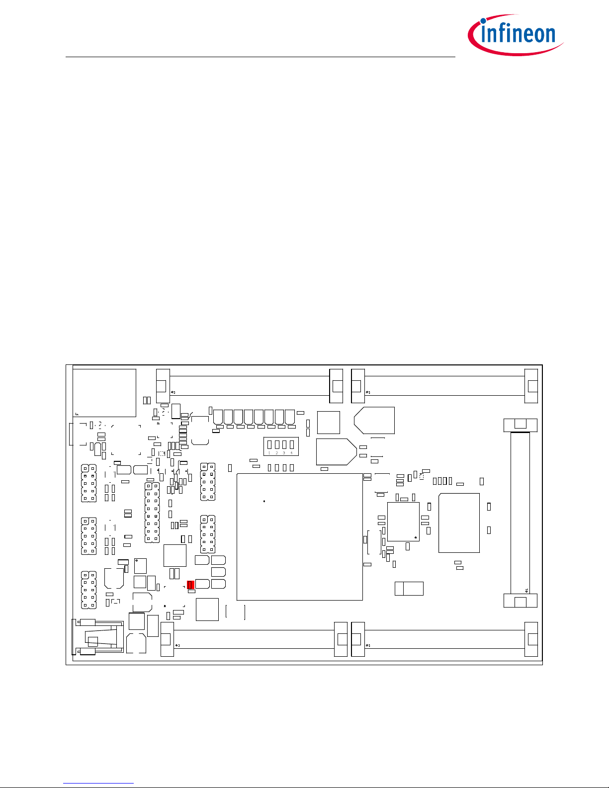
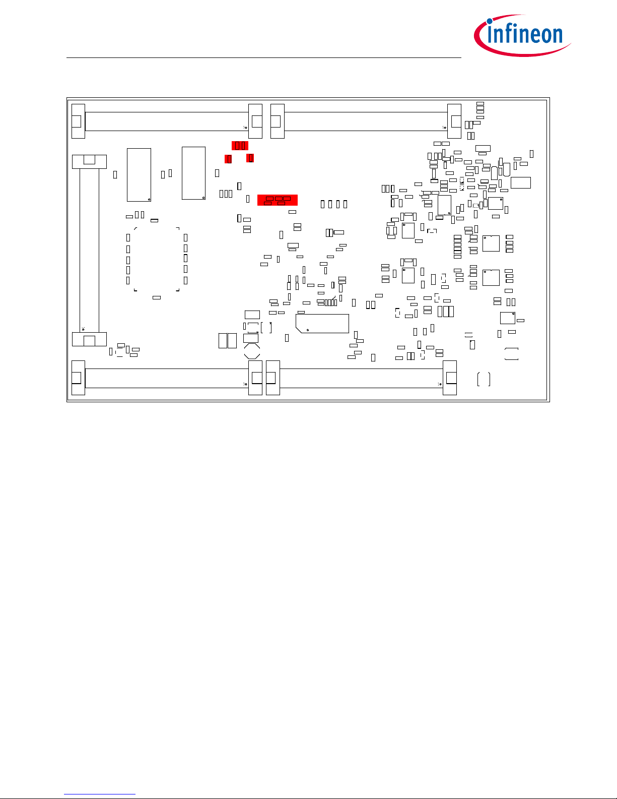
Resistor R508 is red marked in the following Figure 3-1:
Figure 3-1 Resistors for TLF35584 Safety feature handling with switch on
3.4 LEDs
There are 15 LEDs on board:
– D302 up to D305 (blue) -> toogle LEDs connected to P33.4 ... P33.7
Y301
U307
R382
L301
CB319
CB318
C318
C309
C311
U201
R226
R225
S202
R2 56
R255
R217
R205
R204
R203
X403
R453
R329
R390
R601
R376
R375
S201
R377
R381
R380
Q301
CB317
X201
X306
X3 0 5 X304 X303
R236
R234
R2 32
R230
R361
R3 5 9
D301
C310
C306
C303
U408
U407
U406
R451
R455
R456
R454
R446
R444
CB419
CB418
CB417
CB 4 1 6
CB415
CB414
D401
R430
R429
R423
CB405
C402
R411
BU4 0 1
L401
D402
R401
CB401
U404
U401
Y401
CB408
R403
R402
CB402
X402
R344
R424
R4 25
R4 26
R427
R428
R201
R202
C201
C202
R206
R207
Y201
R337R357
R324
R399
R391
R392 R393 R394 R395 R396 R397
R532
C301C302
R439
R531
R335
R336
R355
R356
T301T30 2
X30 1X30 2
X703
D302
D303
D304
D305
D306
D307
D308
D309
D505
D506
D507D504
X4 0 1
S5 0 1
R354
R452
X404
X704
R398
X701
CB607
CB608
CB609
CB610
CB611
CB612
CB613
CB614
CB615
CB6 1 6 CB 617
CB618
CB619
CB620
R603
R605
R607
R608
R606
R604
U603
U604
X705
Q601
R602
R619
R618
R620
R609
R610
R611
X702
X502
CB502
R509
R508
R507
R501
C504
C503
C501
C508
C509
C507
C502
CB501
L501
L502
U501
D508
C505
U502
S502
X501
C320
R3100
R3101
R3102
R3103
R3104
R3108
R3109
R383
X406
X202
R386
Page 11

User Manual 3-3 V2.1
TriBoard TC3X9 TH V2.0(1) and TriBoard TC3X9 V2.0 2017-11
TriBoard Manual TC3X9
Hardware: TriBoard TC3X9 TH V2.0(1) and TriBoard TC3X9 V2.0
TriBoard Information
– D306 up to D309 (blue) -> toogle LEDs connected to P20.11 ... P20.14
– D504 RST (red) -> RESET LED indicate the reset state of the board (/ESR0)
– D505 +1V25 (green) -> +1V25 power supply indication
– D506 +3V3 (green) -> +3,3V power supply indication
– D507 V_UC (green) -> +5V/+3,3V power supply indication
– D508 SS2 (green) -> safe state signal 2 indication
– D402 ACT (green) -> on board miniWiggler JDS is ACTIV
– D401 RUN (blue) -> Debug RUN mode (switched by DAS Server)
3.5 Clock
On the board is a fixed crystal with 20MHz assembled. You can change this by replacing Y101 (soldered).
3.6 External Memory (only with TC399)
The TriBoard supports the following memory configurations:
• up to 4 MBytes external Burst Flash (1x32Bit) or
• up to 2 MBytes external asynchronous SRAM (2x16Bit) or
• up to 4 MBytes external synchronous SRAM (1x32Bit) or
• up to 1 MBytes external asynchronous SRAM (1x16Bit)
For the On Board Memory are reserved chip select 0 and 1. Therefore only two parts, e.g. 1x32Bit Flash and
2x16Bit asynchronous SRAM, should be assembled and can be used at the same time. Chip Select 2 is used as
Burst Address Advance output on the board and can be used externally only if the flash and the sysnchronous
SRAM (if assembled) are not used in burst mode.
3.6.1 External Flash (only with TC399)
The flash uses 32 Data Bits (AD0...AD31) and 20 Address Bits (A0...A19). It’s accessed via /CS0 or /CS1. The flash
has its own resistor to connect to /CS0 or /CS1. To connect the flash see Table 4-4.
Note: Only +3,3V Flash is usable with this board.
3.6.2 External SRAM (only with TC399)
The SRAM uses 32 Data Bits (AD0...AD31) and up to 20 Address Bits (A0...A19).
It’s accessed via /CS0 or /CS1. Each type of SRAM has its own resistor to connect to /CS0 or /CS1. To connect
different SRAMs see Table 4-4.
Note: Only +3,3V SRAM is usable with this board.
3.7 USB Connector
The USB connector is used for connection to a PC. Via the USB it is possible to power the board, using the ASCLIN0
as serial connection via USB and Debugging via DAS. For the pinout of USB socket see Figure 6-5.
NOTE: Before connecting the board to the PC, make sure that the actual DAS software is installed on the PC. For
actual DAS software please contact your local FAE.
The software can also be found on:
DAS website
Page 12
User Manual 3-4 V2.1
TriBoard TC3X9 TH V2.0(1) and TriBoard TC3X9 V2.0 2017-11
TriBoard Manual TC3X9
Hardware: TriBoard TC3X9 TH V2.0(1) and TriBoard TC3X9 V2.0
TriBoard Information
3.7.1 Serial Connection to PC
After the first connection of USB to a PC the needed driver will be installed automatically. During this there will
be created a new COM port on PC. This COM port can be used to communicate with the board via ASCLIN0 of the
device. Per default the ASCLIN0 is used on P14.0 and P14.1 (e.g. Generic Bootstrap Loader) . In case you will use
the Generic Bootstrap Loader via CAN or ASCLIN0 via P15.2 and P15.3 you must:
– remove R436 and R437 (this disconnect the serial connection from P14.0 and P14.1)
– remove R301 and R302 (this disconnect the CAN0 transceiver from P20.7 and P20.8)
– assemble R438 and R440 with 0R resistor (size 0603) to connect P15.2 and P15.3 to serial connection
– assemble R303 and R304 with 0R resistor (size 0603) to connect P14.0 and P14.1 to CAN0 transceiver
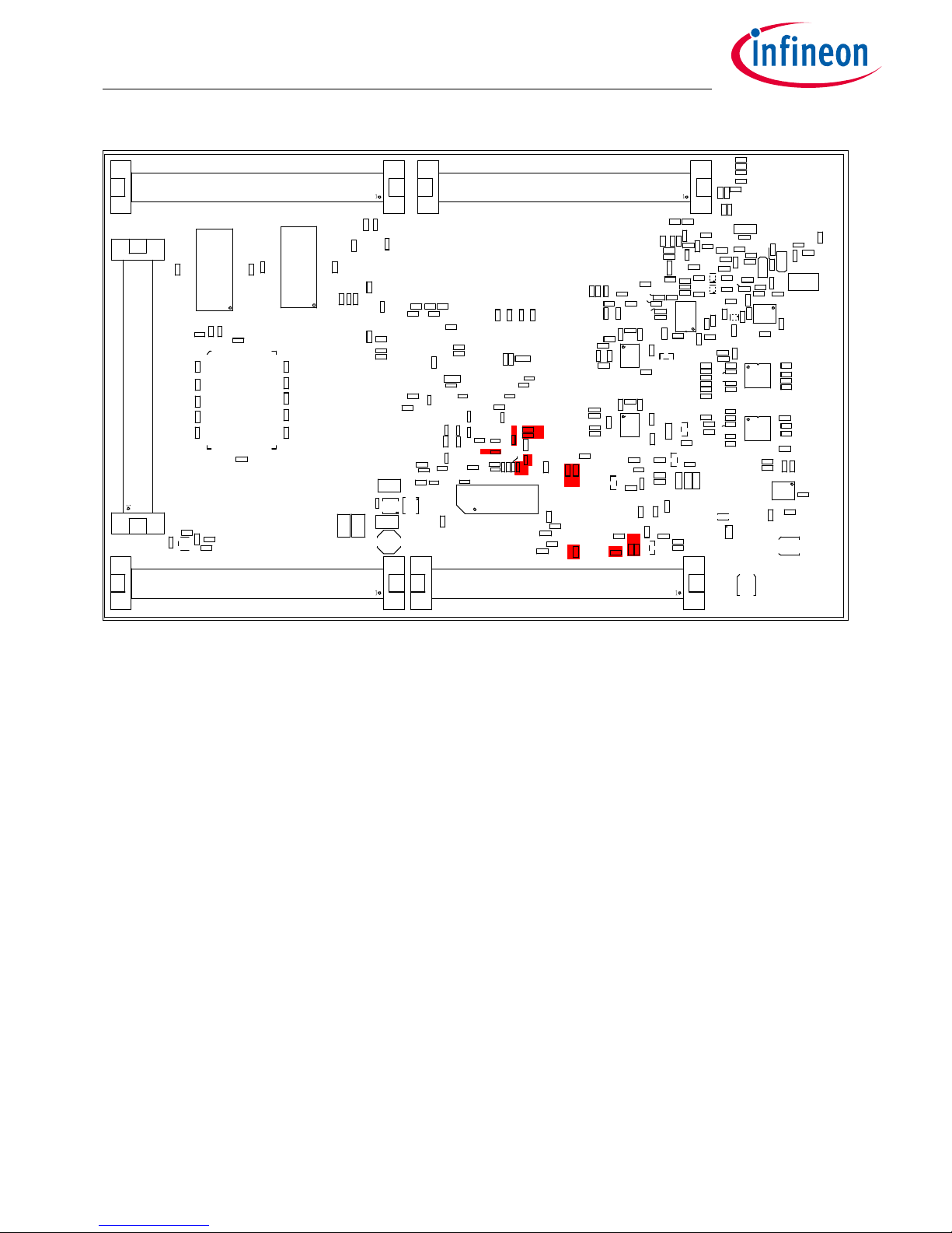
The mentioned resistors are red marked in Figure 3-2.
Figure 3-2 Resistors for ASC connection (ASC0)
3.7.2 miniWiggler JDS
The miniWiggler JDS is a low cost debug tool which allows you access to the JTAG of the device. Make sure that
you have the latest DAS release. Debugging is possible via the DAS Server ‘UDAS‘. Please contact your prefered
debug vendor for support of DAS.
If you have connected the board to the PC and there runs the DAS server, then a working connection is visible via
the green ACTIV LED.
The status RUN LED is switched on/off through the DAS Server, depending on the used debugger (client).
IMPORTANT: Make sure that there is no or a tristated connection on X401 (OCDS1) and X402 (DAP) if the ACTIV LED
is on.
RN301
R249
R248
R247
R246
R245
R244
C208
C207
C2 06
C205
C204
C203
C522
RN302
R241
R239
R237
R235
R233
R231
R224
R219
R218
CB207
R327
R314
R313
R325
R408
R349
R348
R373
R328
R326
R312
D403
R238
R526
R211
CB526
CB525
CB511
CB524
CB523
CB522
CB513
CB203
CB510
CB514
R433
R431
R252
R250
R251R253
R25 4
CB202
R208
CB316
CB315
CB314
CB313
CB312
CB311
R215
R214
R524
X405
U306
R521
R240
R223
R378
R370
R374
R371
R379
R385
R384
R389
R388
R365
R364
R363
R362
R360
R212
Q506
CB206
CB310
C304
C308
C307
C305
R449
R448
R447
R445
R443
R413
U405
L402
CB413
C403
R404
C4 01
R450
R442
R441
CB412
CB411
CB410
C405
C404
R422
R421
U403
Q403
Q402
Q401
R412
C406
R420
R414
R41 9
R418
R416
R415
R410
R409
CB409
CB407
CB403
R440
R407
U402
R406
R405
CB406
CB404
L503
R305
R306
R308
R3 09
R315
R316
R318
R319
R522
R301
R311
R341
R321
R322
R222
R22 0
R221
R525
R523
R533
R323
R343
CB301
CB302
CB205
CB512
CB515
CB516
CB517
CB518
CB520
R537
R307
R317
R538
R534
R513
CB204
CB519
R535
R536
C515
R511
R512
R510
Q502
Q504
Q503
X803
X801
U301U302
R302
R342
CB303
CB304
CB305
CB306
CB307
CB308
CB309
R303
R304
R338
R330
R331
R358
R350
R351
U303
U304
U305
R332
R334
R333
R352
R353
C519
C520
C521
C407
C408
R320
R213
R216
CB2 0 1
R209
R612
R613
R6 14
R615 R616
R617
U601
U602
U605
X805
CB601
CB602
CB603
CB604
CB621
CB622
CB623
CB624 CB625
CB626
CB627
CB628
CB629
CB630
CB631
CB632
R372
X802
R438
R437
R436
R417
R340
R503
D502
C511
C512
D501
Q501
Q505
R506
R502
C510
R504
R505
D503
R520
R346
R347
C312
C313
C314
C315
C316
C317
C506
C319
CB506
R310
R527
R3105
R3106
R3107
R3110
R3111
U503
X804
R457
CB209
L201
R257
R258
R259
R260
CB2 0 8
Page 13

User Manual 3-5 V2.1
TriBoard TC3X9 TH V2.0(1) and TriBoard TC3X9 V2.0 2017-11
TriBoard Manual TC3X9
Hardware: TriBoard TC3X9 TH V2.0(1) and TriBoard TC3X9 V2.0
TriBoard Information
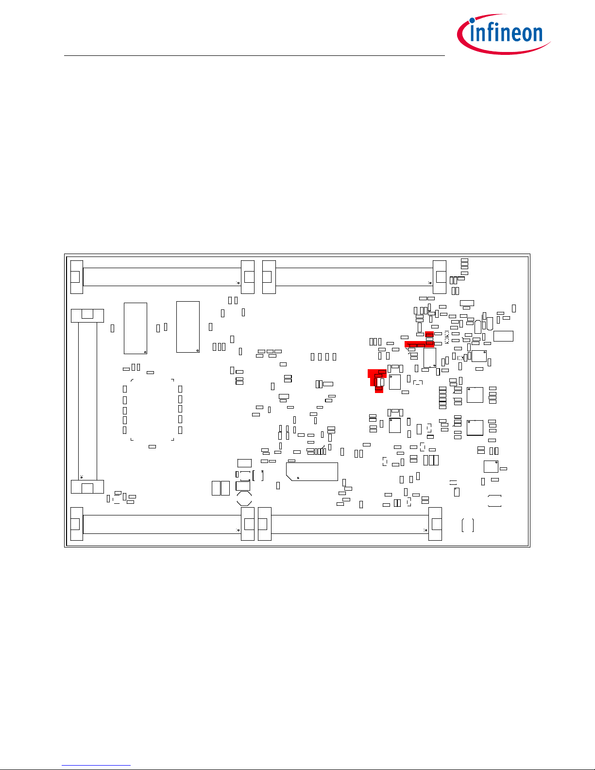
Per default the miniWiggler is connected to the DAP. It is possible to change the connection to DAPE (DAP of
emulation device if available). If resistors R214, R215 and R216 assembled (default) then the standard DAP is
connected to miniWiggler otherwise if R217, R218 and R219 are assembled the the DAPE of enulation device is
connected to miniWiggler. Please note that there should be connected only standard DAP or DAPE. If all this
resistors are not assembled then the miniWiggler can’t be used. In this case only the DAP connectors X402 and
X403 can be used. See Figure 3-5 and Figure 3-6.
3.8 FlexRay™ (E-RAY)
The board has 2 IDC10 plugs for FlexRay™ Communication (channel A and B) with up to 10 Mbit/s. For the pinout
of the plugs see Figure 6-6. You can use a IDC female connector with crimpconnector, flat cable and SUB-D 9 plug
with crimpconnector to have a 1:1 adapter to SUB-D 9.
The transceiver are connected to the TriCore device via zero ohm resistors (R325 up to R329 and R340 up to R344)
which must be removed to use the ports outside.
ERAY-A can be connected to P14.8, P14.9 and P14.10 (default, usable with ERAY0 and ERAY1) and to P02.0, P02.1
and P02.4 (only usable with ERAY0). Transceiver for channel A can be enabled/disabled via P32.3 (default) or via
P10.2. The error state of transceiver channel A can be read out via P32.2 (default) or via P10.1.
ERAY-B is connected to P14.5, P14.6 and P14.7 (default, usable with ERAY0 and ERAY1). Transceiver for channel A
can be enabled/disabled via P20.10 (default). The error state of transceiver channel A can be read out via P20.9
(default).
For more information look in the user manual for TC3X9.
3.9 Serial Eeprom
The I2C via P15.4 and P15.5 of the TC3X9 is connected to a serial EEPROM with a size of 2KBit (2 x 128 x 8). The slave
address of this EEPROM is 0x50. The upper half of the array (80h-FFh) is permanently write-protected. Write
operations to this address range are inhibited. Read operations are not affected. This upper half contains a preprogrammed EUI-48™ node address which can be used as MAC ID for Ethernet. The other 128 bytes are writable
by customer.
To disconnect (disable) the EEPROM remove resistor R348 and R349.
3.10 MultiCAN
On the board are two CAN transceiver connected to the CAN0 and CAN1 of TC3X9. The transceivers are connected
to two IDC10 plug. For the pinout of IDC10 plug see Figure 6-7. You can use a IDC female connector with
crimpconnector, flat cable and SUB-D 9 plug with crimpconnector to have a 1:1 adapter to SUB-D 9.
The transceiver are connected to the TriCore device via zero ohm resistors (R301 up to R304 and R311 up to R314)
which must be removed to use the ports outside.
CAN0 can be used via P20.7 and P20.8 (node 0, default) or P14.0 and P14.1 (node 1). CAN1 can be used via P23.0
and P23.1 (node 0, default) or P00.0 and P00.1 (node 0).
3.11 LIN
On the board is one LIN transceiver connected to the ASCLIN1 on TC3X9 (P15.0 and P15.1). The transceiver are
connected to one IDC10 plug. For the pinout of IDC10 plug see Figure 6-8. You can use a IDC female connector with
crimpconnector, flat cable and SUB-D 9 plug with crimpconnector to have a 1:1 adapter to SUB-D 9.
To disconnect the LIN remove resistor R364 and R365.
Page 14

User Manual 3-6 V2.1
TriBoard TC3X9 TH V2.0(1) and TriBoard TC3X9 V2.0 2017-11
TriBoard Manual TC3X9
Hardware: TriBoard TC3X9 TH V2.0(1) and TriBoard TC3X9 V2.0
TriBoard Information
3.12 Ethernet
The TriBoard provide a RJ45 connector (X306) for twisted pair ethernet connections.The TriBoard use a Realtek
Integrated 10/100/1000M Ethernet Precision Transceiver RTL8211FI-CG as physical interface device. For more
information about the ethernet modul see TC3X9 User’s Manual, about the PHY see the RTL8211F datasheet. For
the pinout of RJ45 see Figure 6-10.
The PHY is connected to the TriCore device via resistors and resistor arrays (R370 up to R374 and RN301 up to
RN302).
For the connection between TriCore and PHY is used RGMII.
Note: Please note that the used signals for RGMII (P11.0 up to P11.12) are not connected to any connector.
3.13 HSCT (optional)
The TriBoard provide a footprint of IEEE 1394 socket (X201 and X202) for connection to other TC3XX via HSCT.
Note: Don’t use X201 and X202 for connection to any IEEE 1394
device, this can destroy the board and/or the connected
device.
X201 is connected to HSCT0 and X202 to HSCT1 of the used device (if used microcontroller support second HSCT).
For connect two TriBoards you need to assemble this socket (Lumberg 2415 01) on each board and connect the
boards with a standard 6 pin IEEE 1394 cable. For the pinout of socket see Figure 6-9.
3.13.1 High speed with HSCT
For use the HSCT connection between two board you need to remove 9 resistors to have a very short connection
between device and connector. On the TC3X9 Triboard this 9 resistors are R250, R251, R252, R253, R254, R257,
R258, R259 and R260 (red marked in Figure 3-3). This resistors needs to be removed.
mportant: When the resistors are removed then the port signals P20.0, P21.2, P21.3, P21.4, P21.5, P21.0, P21.1,
P22.2 and P22.3 are no longer available on the 80 pin samtec connectors.
Page 15
User Manual 3-7 V2.1
TriBoard TC3X9 TH V2.0(1) and TriBoard TC3X9 V2.0 2017-11
TriBoard Manual TC3X9
Hardware: TriBoard TC3X9 TH V2.0(1) and TriBoard TC3X9 V2.0
TriBoard Information
Figure 3-3 Resistors for high speed HSCT
3.14 ADC
On this boards are 6 ADC channels prepared with a low pass filter. On pin AN7, AN20, AN21, AN31, AN44 and AN45
is assembled a capacitor of 47nF and a serial resistor of 4,7K. The filter components are red marked in the
following figure (Figure 3-4).
RN301
R249
R248
R247
R246
R245
R244
C208
C207
C2 06
C205
C204
C203
C522
RN302
R241
R239
R237
R235
R233
R231
R224
R219
R218
CB207
R327
R314
R313
R325
R408
R349
R348
R373
R328
R326
R312
D403
R238
R526
R211
CB526
CB525
CB511
CB524
CB523
CB522
CB513
CB203
CB510
CB514
R433
R431
R252
R250
R251R253
R25 4
CB202
R208
CB316
CB315
CB314
CB313
CB312
CB311
R215
R214
R524
X405
U306
R521
R240
R223
R378
R370
R374
R371
R379
R385
R384
R389
R388
R365
R364
R363
R362
R360
R212
Q506
CB206
CB310
C304
C308
C307
C305
R449
R448
R447
R445
R443
R413
U405
L402
CB413
C403
R404
C4 0 1
R450
R442
R441
CB412
CB411
CB410
C405
C404
R422
R421
U403
Q403
Q402
Q401
R412
C406
R420
R414
R41 9
R418
R416
R415
R410
R409
CB409
CB407
CB403
R440
R407
U402
R406
R405
CB406
CB404
L503
R305
R306
R308
R3 09
R315
R316
R318
R319
R522
R301
R311
R341
R321
R322
R222
R22 0
R221
R525
R523
R533
R323
R343
CB301
CB302
CB205
CB512
CB515
CB516
CB517
CB518
CB520
R537
R307
R317
R538
R534
R513
CB204
CB519
R535
R536
C515
R511
R512
R510
Q502
Q 504
Q503
X803
X801
U301U302
R302
R342
CB303
CB304
CB305
CB306
CB307
CB308
CB309
R303
R304
R338
R330
R331
R358
R350
R351
U303
U304
U305
R332
R334
R333
R352
R353
C519
C520
C521
C407
C408
R320
R213
R216
CB 2 0 1
R209
R612
R613
R6 1 4
R615 R616
R617
U601
U602
U605
X805
CB601
CB602
CB603
CB604
CB621
CB622
CB623
CB624 CB625
CB626
CB627
CB628
CB629
CB630
CB631
CB632
R372
X802
R438
R437
R436
R417
R340
R503
D502
C511
C512
D501
Q501
Q505
R506
R502
C510
R504
R505
D503
R520
R346
R347
C312
C313
C314
C315
C316
C317
C506
C319
CB506
R310
R527
R3 105
R3106
R3107
R3110
R3111
U503
X804
R457
CB209
L201
R257
R258
R259
R260
CB 2 0 8
Page 16
User Manual 3-8 V2.1
TriBoard TC3X9 TH V2.0(1) and TriBoard TC3X9 V2.0 2017-11
TriBoard Manual TC3X9
Hardware: TriBoard TC3X9 TH V2.0(1) and TriBoard TC3X9 V2.0
TriBoard Information
Figure 3-4 Filter components of ADC channels
3.15 Other peripherals
For all other peripherals there are no special plugs on the board. The peripheral signals are available on the
different connectors. See “Connector Pin Assignment” on Page 6-1.
3.16 Toggle LED’s
The status LED’s are low active and can be controlled by Software.
Port 20 pin 11 up to pin 14 are connected to single LED’s (D306... D309) and powered by the normal
microcontroller voltage.
Port 33 pin 4 up to pin 7 are connected to single LED’s (D302... D305) and powered by the standby voltage. This
means that this LED’s can be are activ also when the board is in standby mode and only the standby voltage
available (port 33 is powered by VEVRSB pin which is connected to standby supply of TLF35584). In this case the
port pins are controlled by the standby controller if available.
3.17 Buttons
On the board are three buttons.
The reset button (S501) will apply a warm power on reset to the device.
The ENA button (S502) will be used to enable/wakeup the TLF35584.
The P33.11 button (S202) can be used by software as input. Also can this button used by the standby controller
to react on an event when only standby supply is available (e.g. wakeup the TLF35584 via P33.10).
RN301
R249
R248
R247
R246
R245
R244
C208
C207
C2 06
C205
C204
C203
C522
RN302
R241
R239
R237
R235
R233
R231
R224
R219
R218
CB207
R327
R314
R313
R325
R408
R349
R348
R373
R328
R326
R312
D403
R238
R526
R211
CB526
CB525
CB511
CB524
CB523
CB522
CB513
CB203
CB510
CB514
R433
R431
R252
R250
R251R253
R25 4
CB202
R208
CB316
CB315
CB314
CB313
CB312
CB311
R215
R214
R524
X405
U306
R521
R240
R223
R378
R370
R374
R371
R379
R385
R384
R389
R388
R365
R364
R363
R362
R360
R212
Q506
CB206
CB310
C304
C308
C307
C305
R449
R448
R447
R445
R443
R413
U405
L402
CB413
C403
R404
C4 0 1
R450
R442
R441
CB412
CB411
CB410
C405
C404
R422
R421
U403
Q403
Q402
Q401
R412
C406
R420
R414
R41 9
R418
R416
R415
R410
R409
CB409
CB407
CB403
R440
R407
U402
R406
R405
CB406
CB404
L503
R305
R306
R308
R3 09
R315
R316
R318
R319
R522
R301
R311
R341
R321
R322
R222
R22 0
R221
R525
R523
R533
R323
R343
CB301
CB302
CB205
CB512
CB515
CB516
CB517
CB518
CB520
R537
R307
R317
R538
R534
R513
CB204
CB519
R535
R536
C515
R511
R512
R510
Q502
Q 504
Q503
X803
X801
U301U302
R302
R342
CB303
CB304
CB305
CB306
CB307
CB308
CB309
R303
R304
R338
R330
R331
R358
R350
R351
U303
U304
U305
R332
R334
R333
R352
R353
C519
C520
C521
C407
C408
R320
R213
R216
CB 2 0 1
R209
R612
R613
R6 1 4
R615 R616
R617
U601
U602
U605
X805
CB601
CB602
CB603
CB604
CB621
CB622
CB623
CB624 CB625
CB626
CB627
CB628
CB629
CB630
CB631
CB632
R372
X802
R438
R437
R436
R417
R340
R503
D502
C511
C512
D501
Q501
Q505
R506
R502
C510
R504
R505
D503
R520
R346
R347
C312
C313
C314
C315
C316
C317
C506
C319
CB506
R310
R527
R3 105
R3106
R3107
R3110
R3111
U503
X804
R457
CB209
L201
R257
R258
R259
R260
CB 2 0 8
Page 17

User Manual 3-9 V2.1
TriBoard TC3X9 TH V2.0(1) and TriBoard TC3X9 V2.0 2017-11
TriBoard Manual TC3X9
Hardware: TriBoard TC3X9 TH V2.0(1) and TriBoard TC3X9 V2.0
TriBoard Information
3.18 Debug System
3.18.1 OCDS1
The OCDS1 signals are connected to the IDC16 plug (X401). They work with the port supply of Microcontroller (+5V
default or +3,3V). For pinout of the connector see Figure 6-11. You can connect any debugger to this connector.
The signals /BRKIN and /BRKOUT are not connected per default. If you need this signals in the connector then
assemble R424 and R425 or R426 with a 0R resistor.
If you connect a debug hardware make sure that the miniWiggler JDS (see “miniWiggler JDS” on Page 3-4) is not
activ (ACTIV LED is off) and on the DAP connector (X402) is no hardware connected or the hardware is tristated.
If the ACTIV LED is on, then stop the active DAS Server ’UDAS’ and/or remove the USB connection to the PC.
In case that R217, R218 and R219 are assembled instead of R214, R215 and R216 then the connector can be used
only for DAP connection to DAPE. If R214 up to R219 not assembled then the connector is not usable.
3.18.2 DAP
The board comes with a DAP connector (X402). For pinout of this connector see Figure 6-12. You can connect a
DAP hardware here. If you use this connector make sure that the miniWiggler JDS is not activ (ACTIV LED is off)
and a connected OCDS1 hardware is disconnected or tristated.
3.18.3 DAPE (only Emulation Device)
The board comes also with another DAP connector (X403) which is connected to DAPE in case that an emulation
device is used. For pinout of this connector see Figure 6-12. You can connect a DAP hardware here. In case that
R217, R218 and R219 are assembled (on board miniwiggler connected to DAPE, no default) then make sure that
the miniWiggler JDS is not activ (ACTIV LED is off) and a connected OCDS1 hardware is disconnected or tristated.
3.18.4 DAP_SCR
Additional DAP connector (X406) is connected to DAP_SCR. This DAP can be used as private DAP connection to
the standby controller. For pinout of this connector see Figure 6-12. You can connect a DAP hardware here. This
DAP use P33.6 and P33.7 which are connected to LED on the board. Maybe it is necessary to remove R393 and
R394 if the speed of the connection is not fast enough.
3.18.5 High speed with DAP/DAPE
For use the DAP connection with 160 MHz you need to remove 3 resistors to have a very short connection between
device and connector. On the TC3X9 Triboard this 3 resistors are R214, R215 and R216 for DAP or R217, R218 and
R219 for DAPE (red marked in Figure 3-5 and Figure 3-6). This resistors needs to be removed.
Important: When the resistors are removed then only the DAP and DAPE connector on the board can be used. The
on board wiggler and the OCDS1 connector couldn’t be use (are disconnected) in this case, also the DAP/JTAG
part of AGBT connector and the ETK connector couldn’t be used.
All resistors are red marked in the following figures.
Page 18
User Manual 3-10 V2.1
TriBoard TC3X9 TH V2.0(1) and TriBoard TC3X9 V2.0 2017-11
TriBoard Manual TC3X9
Hardware: TriBoard TC3X9 TH V2.0(1) and TriBoard TC3X9 V2.0
TriBoard Information
Figure 3-5 Location of DAP/DAPE resistors on Top Side
Figure 3-6 Location of DAP/DAPE resistors on Bottom Side
Y301
U307
R382
L301
CB319
CB318
C318
C309
C311
U201
R226
R225
S202
R2 56
R255
R217
R205
R204
R203
X403
R453
R329
R390
R601
R376
R375
S201
R377
R381
R380
Q301
CB317
X201
X306
X3 0 5 X304 X303
R236
R234
R2 32
R230
R361
R3 5 9
D301
C310
C306
C303
U408
U407
U406
R451
R455
R456
R454
R446
R444
CB419
CB418
CB417
CB 4 1 6
CB415
CB414
D401
R430
R429
R423
CB405
C402
R411
BU4 0 1
L401
D402
R401
CB401
U404
U401
Y401
CB408
R403
R402
CB402
X402
R344
R424
R4 25
R4 26
R427
R428
R201
R202
C201
C202
R206
R207
Y201
R337R357
R324
R399
R391
R392 R393 R394 R395 R396 R397
R532
C301C302
R439
R531
R335
R336
R355
R356
T301T30 2
X30 1X30 2
X703
D302
D303
D304
D305
D306
D307
D308
D309
D505
D506
D507D504
X4 0 1
S5 0 1
R354
R452
X404
X704
R398
X701
CB607
CB608
CB609
CB610
CB611
CB612
CB613
CB614
CB615
CB6 1 6 CB617
CB618
CB619
CB620
R603
R605
R607
R608
R606
R604
U603
U604
X705
Q601
R602
R619
R618
R620
R609
R610
R611
X702
X502
CB502
R509
R508
R507
R501
C504
C503
C501
C508
C509
C507
C502
CB501
L501
L502
U501
D508
C505
U502
S502
X501
C320
R3100
R3101
R3102
R3103
R3104
R3108
R3109
R383
X406
X202
R386
RN301
R249
R248
R247
R246
R245
R244
C208
C207
C2 06
C205
C204
C203
C522
RN302
R241
R239
R237
R235
R233
R231
R224
R219
R218
CB207
R327
R314
R313
R325
R408
R349
R348
R373
R328
R326
R312
D403
R238
R526
R211
CB526
CB525
CB511
CB524
CB523
CB522
CB513
CB203
CB510
CB514
R433
R431
R252
R250
R251R253
R25 4
CB202
R208
CB316
CB315
CB314
CB313
CB312
CB311
R215
R214
R524
X405
U306
R521
R240
R223
R378
R370
R374
R371
R379
R385
R384
R389
R388
R365
R364
R363
R362
R360
R212
Q506
CB206
CB310
C304
C308
C307
C305
R449
R448
R447
R445
R443
R413
U405
L402
CB413
C403
R404
C4 0 1
R450
R442
R441
CB412
CB411
CB410
C405
C404
R422
R421
U403
Q403
Q402
Q401
R412
C406
R420
R414
R41 9
R418
R416
R415
R410
R409
CB409
CB407
CB403
R440
R407
U402
R406
R405
CB406
CB404
L503
R305
R306
R308
R3 09
R315
R316
R318
R319
R522
R301
R311
R341
R321
R322
R222
R22 0
R221
R525
R523
R533
R323
R343
CB301
CB302
CB205
CB512
CB515
CB516
CB517
CB518
CB520
R537
R307
R317
R538
R534
R513
CB204
CB519
R535
R536
C515
R511
R512
R510
Q502
Q 504
Q503
X803
X801
U301U302
R302
R342
CB303
CB304
CB305
CB306
CB307
CB308
CB309
R303
R304
R338
R330
R331
R358
R350
R351
U303
U304
U305
R332
R334
R333
R352
R353
C519
C520
C521
C407
C408
R320
R213
R216
CB 2 0 1
R209
R612
R613
R6 1 4
R615 R616
R617
U601
U602
U605
X805
CB601
CB602
CB603
CB604
CB621
CB622
CB623
CB624 CB625
CB626
CB627
CB628
CB629
CB630
CB631
CB632
R372
X802
R438
R437
R436
R417
R340
R503
D502
C511
C512
D501
Q501
Q505
R506
R502
C510
R504
R505
D503
R520
R346
R347
C312
C313
C314
C315
C316
C317
C506
C319
CB506
R310
R527
R3 105
R3106
R3107
R3110
R3111
U503
X804
R457
CB209
L201
R257
R258
R259
R260
CB 2 0 8
Page 19

User Manual 3-11 V2.1
TriBoard TC3X9 TH V2.0(1) and TriBoard TC3X9 V2.0 2017-11
TriBoard Manual TC3X9
Hardware: TriBoard TC3X9 TH V2.0(1) and TriBoard TC3X9 V2.0
TriBoard Information
3.18.6 AGBT (optional)
The TriBoard provide a 22 pin high speed samtec connector (X405) for highest speed connection via AGBT. This
connector should be assembled by your self if needed.
The AGBT interface is only available on emulation devices.
For the pinout of connector see Figure 6-15.
The needed Samtec connector is: ASP-137969-01 (serie ERM8, Nexus HS22).
3.18.7 ETK connector (optional)
The TriBoard provide a 10 pin samtec connector (X404) for connecting to an ETK. This connector should be
assembled by your self if needed.
For the pinout of connector see Figure 6-13.
The needed Samtec connector is: TFM-105-02-A.
3.18.8 EmW Power (optional)
The TriBoard provide the 4 pin power connector (X502) for the Ethernet miniWiggler (EmW). This connector
should be assembled by your self if needed.
For the pinout of connector see Figure 6-14.
The needed Samtec connector is the JST B4B-PH-K.
The connector provide the input voltage to the Ethernet miniWiggler and an enable/wakeup signal connected to
TLF35584 and a standby voltage of +1,25V connected to VDDSB of device. In case the EmW is used you must
remove R522. If R522 is removed then you must make sure that the EmW is always connected. Otherwise with
assembled R522 (default) you should not connect the pin 4 of connector.
The mentioned resistor is red marked in Figure 3-7:
Page 20

User Manual 3-12 V2.1
TriBoard TC3X9 TH V2.0(1) and TriBoard TC3X9 V2.0 2017-11
TriBoard Manual TC3X9
Hardware: TriBoard TC3X9 TH V2.0(1) and TriBoard TC3X9 V2.0
TriBoard Information
Figure 3-7 Resistor for VDDSB
RN301
R249
R248
R247
R246
R245
R244
C208
C207
C2 06
C205
C204
C203
C522
RN302
R241
R239
R237
R235
R233
R231
R224
R219
R218
CB207
R327
R314
R313
R325
R408
R349
R348
R373
R328
R326
R312
D403
R238
R526
R211
CB526
CB525
CB511
CB524
CB523
CB522
CB513
CB203
CB510
CB514
R433
R431
R252
R250
R251R253
R25 4
CB202
R208
CB316
CB315
CB314
CB313
CB312
CB311
R215
R214
R524
X405
U306
R521
R240
R223
R378
R370
R374
R371
R379
R385
R384
R389
R388
R365
R364
R363
R362
R360
R212
Q506
CB206
CB310
C304
C308
C307
C305
R449
R448
R447
R445
R443
R413
U405
L402
CB413
C403
R404
C4 0 1
R450
R442
R441
CB412
CB411
CB410
C405
C404
R422
R421
U403
Q403
Q402
Q401
R412
C406
R420
R414
R41 9
R418
R416
R415
R410
R409
CB409
CB407
CB403
R440
R407
U402
R406
R405
CB406
CB404
L503
R305
R306
R308
R3 09
R315
R316
R318
R319
R522
R301
R311
R341
R321
R322
R222
R22 0
R221
R525
R523
R533
R323
R343
CB301
CB302
CB205
CB512
CB515
CB516
CB517
CB518
CB520
R537
R307
R317
R538
R534
R513
CB204
CB519
R535
R536
C515
R511
R512
R510
Q502
Q 504
Q503
X803
X801
U301U302
R302
R34 2
CB303
CB304
CB305
CB306
CB307
CB308
CB309
R303
R304
R338
R330
R331
R358
R350
R351
U303
U304
U305
R332
R334
R333
R352
R353
C519
C520
C521
C407
C408
R320
R213
R216
CB 2 0 1
R209
R612
R613
R6 1 4
R615 R616
R617
U601
U602
U605
X805
CB601
CB602
CB603
CB604
CB621
CB622
CB623
CB624 CB625
CB626
CB627
CB628
CB629
CB630
CB631
CB632
R372
X802
R438
R437
R436
R417
R340
R503
D502
C511
C512
D501
Q501
Q505
R506
R502
C510
R504
R505
D503
R520
R346
R347
C312
C313
C314
C315
C316
C317
C506
C319
CB506
R310
R527
R3 105
R3106
R3107
R3110
R3111
U503
X804
R457
CB209
L201
R257
R258
R259
R260
CB 2 0 8
Page 21

User Manual 4-1 V2.1
TriBoard TC3X9 TH V2.0(1) and TriBoard TC3X9 V2.0 2017-11
TriBoard Manual TC3X9
Hardware: TriBoard TC3X9 TH V2.0(1) and TriBoard TC3X9 V2.0
TriBoard Configuration
4 TriBoard Configuration
4.1 HW Boot Configuration
Figure 4-1 HW Configuration DIP-Switches
The picture above shows the definition of the boot HW configuration switch. The meaning of the switches will be
described in the following table (Table 4-1).
Note:
The ON position of the switch is equal to a logical LOW at the dedicated pin.
4.1.1 Default Pad State
P14.4 / HWCFG6 is used to select the Default Pad State. Dipswitch 1 used to select this.
In case that dispswitch1 is set to ON then all I/O pins are in tristate otherwise the internal pull-up devices are
enabled on the I/O pins. Please note that after change Dipswitch 1 you must make a power cycle (switch off ->
switch on) to use the new configuration.
In case that TriState is selected (Dipswitch 1 is set to ON) then the I/O pins are floating. If you need a specific level
on different pins during startup (e.g. driver pins) then you must add the needed pull device (up or down). Some
pins (especially the HWCFG pins) haven always the needed external pull-up and/or pull-down resistor assembled
on the board.
4.1.2 Bootmode
Table 4-1 User Startup Modes
1)2)3)
1) The shadowed line indicates the default setting.
2) ’x’ represents the don’t care state.
3) 2 to 4 are the Dip Switch numbers.
HWCFG[5...3] Type of Boot 2 3 4
XX1 Start-up mode is selected by Boot Mode Index X X OFF
110 Internal Start from Flash OFF OFF ON
100 Alternate Boot Mode, Generic Bootstrap Loader on fail (P14.0/P14.1) ON OFF ON
010 Alternate Boot Mode, ASC Bootstrap Loader on fail (P15.2/P15.3) OFF ON ON
000 Generic Bootstrap Loader (P14.0/P14.1) ON ON ON
2
on
134
P14
.
4
P10.5
P10
.
6
P14
.
3
Page 22

User Manual 4-2 V2.1
TriBoard TC3X9 TH V2.0(1) and TriBoard TC3X9 V2.0 2017-11
TriBoard Manual TC3X9
Hardware: TriBoard TC3X9 TH V2.0(1) and TriBoard TC3X9 V2.0
TriBoard Configuration
4.2 Assembly Options
4.2.1 General optional resistors
Note: All resistors are red marked in the following figures.
Table 4-2 General optional resistors (default assembly in brackets)
Component Description
R202 Connect P20.2 (/TESTMODE) to GND (not assembled)
R203 XTAL1 Rload (50 Ohm) (not assembled)
R206 XTAL Rparallel (not assembled)
R207 XTAL2 Rserial (assembled)
R238 Switch off EVRC (not assembled)
R240 Switch off EVR33 (not assembled)
R390 Connect V_STBY to toggle LEDs D302...D305 (assembled)
R399 Connect V_UC to toggle LEDs D306...D309 (assembled)
R423 Connect P20.0 with miniWiggler JDS (not assembled)
R424 Connect P20.0 with OCDS1 connector (not assembled)
R425 Connect P20.1 with OCDS1 connector (not assembled)
R426 Connect P20.2 with OCDS1 connector (not assembled)
R427 Connect P20.1 with USR1 of miniWiggler JDS (not assembled)
R428 Connect P20.2 with USR1 of miniWiggler JDS (not assembled)
R429 Connect P21.6 (DAP3) with USR1 of DAP (assembled)
R430 Connect P20.2 with USR1 of DAP (not assembled)
R433 Connect P20.1 with ETK connector (not assembled)
R439 Connect P21.7 with ETK connector (not assembled)
R508 Connect pin MPS of TLF35584 to V_CO (assembled)
R524 Connect VDDP3 to V_UC (not assembled)
R525 Connect VDDP3 to +3V3 (not assembled)
R526 Connect VEBU/VEXT to +3V3 (assembled if external memory assembled, not usable with
TC389)
R527 Connect VEBU/VEXT to V_UC (assembled if no external memory assembled)
Page 23

User Manual 4-3 V2.1
TriBoard TC3X9 TH V2.0(1) and TriBoard TC3X9 V2.0 2017-11
TriBoard Manual TC3X9
Hardware: TriBoard TC3X9 TH V2.0(1) and TriBoard TC3X9 V2.0
TriBoard Configuration
Figure 4-2 Location of general optional resistors on Top Side
Figure 4-3 Location of general optional resistors on Bottom Side
Y301
U307
R382
L301
CB319
CB318
C318
C309
C311
U201
R226
R225
S202
R2 56
R255
R217
R205
R204
R203
X403
R453
R329
R390
R601
R376
R375
S201
R377
R381
R380
Q301
CB317
X201
X306
X3 0 5 X304 X303
R236
R234
R2 32
R230
R361
R3 5 9
D301
C310
C306
C303
U408
U407
U406
R451
R455
R456
R454
R446
R444
CB419
CB418
CB417
CB 4 1 6
CB415
CB414
D401
R430
R429
R423
CB405
C402
R411
BU4 0 1
L401
D402
R401
CB401
U404
U401
Y401
CB408
R403
R402
CB402
X402
R344
R424
R4 25
R4 26
R427
R428
R201
R202
C201
C202
R206
R207
Y201
R337R357
R324
R399
R391
R392 R393 R394 R395 R396 R397
R532
C301C302
R439
R531
R335
R336
R355
R356
T301T30 2
X30 1X30 2
X703
D302
D303
D304
D305
D306
D307
D308
D309
D505
D506
D507D504
X4 0 1
S5 0 1
R354
R452
X404
X704
R398
X701
CB607
CB608
CB609
CB610
CB611
CB612
CB613
CB614
CB615
CB6 1 6 CB617
CB618
CB619
CB620
R603
R605
R607
R608
R606
R604
U603
U604
X705
Q601
R602
R619
R618
R620
R609
R610
R611
X702
X502
CB502
R509
R508
R507
R501
C504
C503
C501
C508
C509
C507
C502
CB501
L501
L502
U501
D508
C505
U502
S502
X501
C320
R3100
R3101
R3102
R3103
R3104
R3108
R3109
R383
X406
X202
R386
RN301
R249
R248
R247
R246
R245
R244
C208
C207
C2 06
C205
C204
C203
C522
RN302
R241
R239
R237
R235
R233
R231
R224
R219
R218
CB207
R327
R314
R313
R325
R408
R349
R348
R373
R328
R326
R312
D403
R238
R526
R211
CB526
CB525
CB511
CB524
CB523
CB522
CB513
CB203
CB510
CB514
R433
R431
R252
R250
R251R253
R25 4
CB202
R208
CB316
CB315
CB314
CB313
CB312
CB311
R215
R214
R524
X405
U306
R521
R240
R223
R378
R370
R374
R371
R379
R385
R384
R389
R388
R365
R364
R363
R362
R360
R212
Q506
CB206
CB310
C304
C308
C307
C305
R449
R448
R447
R445
R443
R413
U405
L402
CB413
C403
R404
C4 0 1
R450
R442
R441
CB412
CB411
CB410
C405
C404
R422
R421
U403
Q403
Q402
Q401
R412
C406
R420
R414
R41 9
R418
R416
R415
R410
R409
CB409
CB407
CB403
R440
R407
U402
R406
R405
CB406
CB404
L503
R305
R306
R308
R3 09
R315
R316
R318
R319
R522
R301
R311
R341
R321
R322
R222
R22 0
R221
R525
R523
R533
R323
R343
CB301
CB302
CB205
CB512
CB515
CB516
CB517
CB518
CB520
R537
R307
R317
R538
R534
R513
CB204
CB519
R535
R536
C515
R511
R512
R510
Q502
Q 504
Q503
X803
X801
U301U302
R302
R34 2
CB303
CB304
CB305
CB306
CB307
CB308
CB309
R303
R304
R338
R330
R331
R358
R350
R351
U303
U304
U305
R332
R334
R333
R352
R353
C519
C520
C521
C407
C408
R320
R213
R216
CB 2 0 1
R209
R612
R613
R6 1 4
R615 R616
R617
U601
U602
U605
X805
CB601
CB602
CB603
CB604
CB621
CB622
CB623
CB624 CB625
CB626
CB627
CB628
CB629
CB630
CB631
CB632
R372
X802
R438
R437
R436
R417
R340
R503
D502
C511
C512
D501
Q501
Q505
R506
R502
C510
R504
R505
D503
R520
R346
R347
C312
C313
C314
C315
C316
C317
C506
C319
CB506
R310
R527
R3 105
R3106
R3107
R3110
R3111
U503
X804
R457
CB209
L201
R257
R258
R259
R260
CB 2 0 8
Page 24

User Manual 4-4 V2.1
TriBoard TC3X9 TH V2.0(1) and TriBoard TC3X9 V2.0 2017-11
TriBoard Manual TC3X9
Hardware: TriBoard TC3X9 TH V2.0(1) and TriBoard TC3X9 V2.0
TriBoard Configuration
4.2.2 Resistors for peripherals
Table 4-3 Resistors for peripherals (default assembly in brackets)
Component Description
R220 Connect V_VR with VDDM (assembled)
R221 Connect +3V3 with VDDM (not assembled)
R222 Connect VAREF1 with VDDM (assembled)
R223 Connect VAREF2 with VDDM (assembled)
R224 Connect VAREF3 with VDDM (assembled)
R301 Connect P20.7 with RXD of CAN0 transceiver (assembled)
R302 Connect P20.8 with TXD of CAN0 transceiver (assembled)
R303 Connect P14.1 with RXD of CAN0 transceiver (not assembled)
R304 Connect P14.0 with TXD of CAN0 transceiver (not assembled)
R311 Connect P23.0 with RXD of CAN1 transceiver (assembled)
R312 Connect P23.1 with TXD of CAN1 transceiver (assembled)
R313 Connect P00.1 with RXD of CAN1 transceiver (not assembled)
R314 Connect P00.0 with TXD of CAN1 transceiver (not assembled)
R320 Connect P14.10 with TXD of ERAY-A transceiver (assembled)
R321 Connect P14.9 with TXDEN of ERAY-A transceiver (assembled)
R322 Connect P14.8 with RXD of ERAY-A transceiver (assembled)
R323 Connect P32.3 with EN of ERAY-A transceiver (assembled)
R324 Connect P32.2 with ERRN of ERAY-A transceiver (assembled)
R325 Connect P02.1 with RXD of ERAY-A transceiver (not assembled)
R326 Connect P02.4 with TXDEN of ERAY-A transceiver (not assembled)
R327 Connect P02.0 with TXD of ERAY-A transceiver (not assembled)
R328 Connect P10.2 with EN of ERAY-A transceiver (not assembled)
R329 Connect P10.1 with ERRN of ERAY-A transceiver (not assembled)
R340 Connect P14.5 with TXD of ERAY-B transceiver (assembled)
R341 Connect P14.6 with TXDEN of ERAY-B transceiver (assembled)
R342 Connect P14.7 with RXD of ERAY-B transceiver (assembled)
R343 Connect P20.10 with EN of ERAY-B transceiver (assembled)
R344 Connect P20.9 with ERRN of ERAY-B transceiver (assembled)
R348 Connect P15.4 with SCL of I2C Eeprom (assembled)
R349 Connect P15.5 with SDA of I2C Eeprom (assembled)
R364 Connect P15.1 with RXD of LIN1 transceiver (assembled)
R365 Connect P15.0 with TXD of LIN1 transceiver (assembled)
R310 Connect P11.5 with CLOCKOUT of Ethernet PHY (assembled)
R370 Connect P11.12 with RXC of Ethernet PHY (assembled)
R371 Connect CLKOUT of Ethernet PHY with TXC of Ethernet PHY (not assembled)
R372 Connect P11.11 with RXCTL of Ethernet PHY (assembled)
Page 25

User Manual 4-5 V2.1
TriBoard TC3X9 TH V2.0(1) and TriBoard TC3X9 V2.0 2017-11
TriBoard Manual TC3X9
Hardware: TriBoard TC3X9 TH V2.0(1) and TriBoard TC3X9 V2.0
TriBoard Configuration
Note: All resistors are red marked in the following figures
Figure 4-4 Location of peripheral resistors on Top Side
R373 Connect P11.4 with TXC of Ethernet PHY (assembled)
R374 Connect P11.6 with TXCTL of Ethernet PHY (assembled)
R375 Connect P12.1 with MDIO of Ethernet PHY (assembled)
R376 Connect P12.0 with MDC of Ethernet PHY (assembled)
R377 Connect P15.8 with MDINT of Ethernet PHY (not assembled)
RN301 Connect P11.7...10 with RDX3...0 of Ethernet PHY (assembled)
RN302 Connect P11.0...3 with TDX3...0 of Ethernet PHY (assembled)
R436 Connect P14.0 with RXD of USB to UART (assembled)
R437 Connect P14.1 with TXD of USB to UART (assembled)
R438 Connect P15.2 with RXD of USB to UART (not assembled)
R440 Connect P15.3 with TXD of USB to UART (not assembled)
Table 4-3 Resistors for peripherals (default assembly in brackets) (continued)
Component Description
Y301
U307
R382
L301
CB319
CB318
C318
C309
C311
U201
R226
R225
S202
R2 56
R255
R217
R205
R204
R203
X403
R453
R329
R390
R601
R376
R375
S201
R377
R381
R380
Q301
CB317
X201
X306
X3 0 5 X304 X303
R236
R234
R2 32
R230
R361
R3 5 9
D301
C310
C306
C303
U408
U407
U406
R451
R455
R456
R454
R446
R444
CB419
CB418
CB417
CB 4 1 6
CB415
CB414
D401
R430
R429
R423
CB405
C402
R411
BU4 0 1
L401
D402
R401
CB401
U404
U401
Y401
CB408
R403
R402
CB402
X402
R344
R424
R4 25
R4 26
R427
R428
R201
R202
C201
C202
R206
R207
Y201
R337R357
R324
R399
R391
R392 R393 R394 R395 R396 R397
R532
C301C302
R439
R531
R335
R336
R355
R356
T301T30 2
X30 1X30 2
X703
D302
D303
D304
D305
D306
D307
D308
D309
D505
D506
D507D504
X4 0 1
S5 0 1
R354
R452
X404
X704
R398
X701
CB607
CB608
CB609
CB610
CB611
CB612
CB613
CB614
CB615
CB6 1 6 CB 617
CB618
CB619
CB620
R603
R605
R607
R608
R606
R604
U603
U604
X705
Q601
R602
R619
R618
R620
R609
R610
R611
X702
X502
CB502
R509
R508
R507
R501
C504
C503
C501
C508
C509
C507
C502
CB501
L501
L502
U501
D508
C505
U502
S502
X501
C320
R3100
R3101
R3102
R3103
R3104
R3108
R3109
R383
X406
X202
R386
Page 26

User Manual 4-6 V2.1
TriBoard TC3X9 TH V2.0(1) and TriBoard TC3X9 V2.0 2017-11
TriBoard Manual TC3X9
Hardware: TriBoard TC3X9 TH V2.0(1) and TriBoard TC3X9 V2.0
TriBoard Configuration
Figure 4-5 Location of peripheral resistors on Bottom Side
4.2.3 Resistors for memories
Note: All resistors are red marked in the following figures
Table 4-4 Resistors for memories (default assembly in brackets)
Component Description
R612 Connect /CS1 to 16-bit SRAMs (assembled)
R613 Connect /CS0 to 16-bit SRAMs (not assembled)
R615 Connect /CS1 to 32-bit SRAM (not assembled)
R616 Connect /CS0 to 32-bit SRAM (not assembled)
R618 Connect /CS1 to 32-bit Flash (not assembled)
R619 Connect /CS0 to 32-bit Flash (assembled)
RN301
R249
R248
R247
R246
R245
R244
C208
C207
C2 06
C205
C204
C203
C522
RN302
R241
R239
R237
R235
R233
R231
R224
R219
R218
CB207
R327
R314
R313
R325
R408
R349
R348
R373
R328
R326
R312
D403
R238
R526
R211
CB526
CB525
CB511
CB524
CB523
CB522
CB513
CB203
CB510
CB514
R433
R431
R252
R250
R251R253
R25 4
CB202
R208
CB316
CB315
CB314
CB313
CB312
CB311
R215
R214
R524
X405
U306
R521
R240
R223
R378
R370
R374
R371
R379
R385
R384
R389
R388
R365
R364
R363
R362
R360
R212
Q506
CB206
CB310
C304
C308
C307
C305
R449
R448
R447
R445
R443
R413
U405
L402
CB413
C403
R404
C4 0 1
R450
R442
R441
CB412
CB411
CB410
C405
C404
R422
R421
U403
Q403
Q402
Q401
R412
C406
R420
R414
R41 9
R418
R416
R415
R410
R409
CB409
CB407
CB403
R440
R407
U402
R406
R405
CB406
CB404
L503
R305
R306
R308
R3 09
R315
R316
R318
R319
R522
R301
R311
R341
R321
R322
R222
R22 0
R221
R525
R523
R533
R323
R343
CB301
CB302
CB205
CB512
CB515
CB516
CB517
CB518
CB520
R537
R307
R317
R538
R534
R513
CB204
CB519
R535
R536
C515
R511
R512
R510
Q502
Q 504
Q503
X803
X801
U301U302
R302
R34 2
CB303
CB304
CB305
CB306
CB307
CB308
CB309
R303
R304
R338
R330
R331
R358
R350
R351
U303
U304
U305
R332
R334
R333
R352
R353
C519
C520
C521
C407
C408
R320
R213
R216
CB 2 0 1
R209
R612
R613
R6 1 4
R615 R616
R617
U601
U602
U605
X805
CB601
CB602
CB603
CB604
CB621
CB622
CB623
CB624 CB625
CB626
CB627
CB628
CB629
CB630
CB631
CB632
R372
X802
R438
R437
R436
R417
R340
R503
D502
C511
C512
D501
Q501
Q505
R506
R502
C510
R504
R505
D503
R520
R346
R347
C312
C313
C314
C315
C316
C317
C506
C319
CB506
R310
R527
R3 105
R3106
R3107
R3110
R3111
U503
X804
R457
CB209
L201
R257
R258
R259
R260
CB 2 0 8
Page 27

User Manual 4-7 V2.1
TriBoard TC3X9 TH V2.0(1) and TriBoard TC3X9 V2.0 2017-11
TriBoard Manual TC3X9
Hardware: TriBoard TC3X9 TH V2.0(1) and TriBoard TC3X9 V2.0
TriBoard Configuration
Figure 4-6 Location of memories resistors on Top Side
Figure 4-7 Location of memories resistors on Bottom Side
Y301
U307
R382
L301
CB319
CB318
C318
C309
C311
U201
R226
R225
S202
R2 56
R255
R217
R205
R204
R203
X403
R453
R329
R390
R601
R376
R375
S201
R377
R381
R380
Q301
CB317
X201
X306
X3 0 5 X304 X303
R236
R234
R2 32
R230
R361
R3 5 9
D301
C310
C306
C303
U408
U407
U406
R451
R455
R456
R454
R446
R444
CB419
CB418
CB417
CB 4 1 6
CB415
CB414
D401
R430
R429
R423
CB405
C402
R411
BU4 0 1
L401
D402
R401
CB401
U404
U401
Y401
CB408
R403
R402
CB402
X402
R344
R424
R4 25
R4 26
R427
R428
R201
R202
C201
C202
R206
R207
Y201
R337R357
R324
R399
R391
R392 R393 R394 R395 R396 R397
R532
C301C302
R439
R531
R335
R336
R355
R356
T301T30 2
X30 1X30 2
X703
D302
D303
D304
D305
D306
D307
D308
D309
D505
D506
D507D504
X4 0 1
S5 0 1
R354
R452
X404
X704
R398
X701
CB607
CB608
CB609
CB610
CB611
CB612
CB613
CB614
CB615
CB6 1 6 CB617
CB618
CB619
CB620
R603
R605
R607
R608
R606
R604
U603
U604
X705
Q601
R602
R619
R618
R620
R609
R610
R611
X702
X502
CB502
R509
R508
R507
R501
C504
C503
C501
C508
C509
C507
C502
CB501
L501
L502
U501
D508
C505
U502
S502
X501
C320
R3100
R3101
R3102
R3103
R3104
R3108
R3109
R383
X406
X202
R386
RN301
R249
R248
R247
R246
R245
R244
C208
C207
C2 06
C205
C204
C203
C522
RN302
R241
R239
R237
R235
R233
R231
R224
R219
R218
CB207
R327
R314
R313
R325
R408
R349
R348
R373
R328
R326
R312
D403
R238
R526
R211
CB526
CB525
CB511
CB524
CB523
CB522
CB513
CB203
CB510
CB514
R433
R431
R252
R250
R251R253
R25 4
CB202
R208
CB316
CB315
CB314
CB313
CB312
CB311
R215
R214
R524
X405
U306
R521
R240
R223
R378
R370
R374
R371
R379
R385
R384
R389
R388
R365
R364
R363
R362
R360
R212
Q506
CB206
CB310
C304
C308
C307
C305
R449
R448
R447
R445
R443
R413
U405
L402
CB413
C403
R404
C4 0 1
R450
R442
R441
CB412
CB411
CB410
C405
C404
R422
R421
U403
Q403
Q402
Q401
R412
C406
R420
R414
R41 9
R418
R416
R415
R410
R409
CB409
CB407
CB403
R440
R407
U402
R406
R405
CB406
CB404
L503
R305
R306
R308
R3 09
R315
R316
R318
R319
R522
R301
R311
R341
R321
R322
R222
R22 0
R221
R525
R523
R533
R323
R343
CB301
CB302
CB205
CB512
CB515
CB516
CB517
CB518
CB520
R537
R307
R317
R538
R534
R513
CB204
CB519
R535
R536
C515
R511
R512
R510
Q502
Q 504
Q503
X803
X801
U301U302
R302
R34 2
CB303
CB304
CB305
CB306
CB307
CB308
CB309
R303
R304
R338
R330
R331
R358
R350
R351
U303
U304
U305
R332
R334
R333
R352
R353
C519
C520
C521
C407
C408
R320
R213
R216
CB 2 0 1
R209
R612
R613
R6 1 4
R615 R616
R617
U601
U602
U605
X805
CB601
CB602
CB603
CB604
CB621
CB622
CB623
CB624 CB625
CB626
CB627
CB628
CB629
CB630
CB631
CB632
R372
X802
R438
R437
R436
R417
R340
R503
D502
C511
C512
D501
Q501
Q505
R506
R502
C510
R504
R505
D503
R520
R346
R347
C312
C313
C314
C315
C316
C317
C506
C319
CB506
R310
R527
R3 105
R3106
R3107
R3110
R3111
U503
X804
R457
CB209
L201
R257
R258
R259
R260
CB 2 0 8
Page 28

User Manual 5-1 V2.1
TriBoard TC3X9 TH V2.0(1) and TriBoard TC3X9 V2.0 2017-11
TriBoard Manual TC3X9
Hardware: TriBoard TC3X9 TH V2.0(1) and TriBoard TC3X9 V2.0
Signal (on board used) Description
5 Signal (on board used) Description
For more information about the signals please see the user manual/datasheet for TC3X9 and/or the schematics
of the board.
All not mentioned signals are not used on the board and can be used outside. Optional marked signals are used
only if they are connected (default is that they are not used on the board).
5.1 Power Signals
5.2 Reset Signals
Table 5-1 Power Signals
Short name Description
VCC_IN Supply Input (3,5V...40V)
VIN Input Voltage of Power Supply Device
GND Ground
V_PREPEG Pre Regulator Voltage (~5,8V)
V_UC Microcontroller Supply Voltage (5V or 3,3V depends on assembled TLF35584)
V_CO Communication Supply Voltage (5V)
V_VR Reference Supply Voltage (5V)
V_STBY Standby Supply Voltage (5V or 3,3V depends on assembled TLF35584)
VDD Core Supply Voltage (1,25V)
VDDSB Emulation Stand-by SRAM Supply Voltage (1,25V)
VDDP3 Flash Power Supply Voltage (3,3V)
VFLEX Flexport Supply Voltage (3,3V)
VEBU EBU Supply Voltage (3,3V)
VEXTOSC Oscillator Port Supply Voltage (5V or 3,3V depends on assembled TLF35584)
VDDOSC Oscillator Core Supply Voltage (1,25V)
VSSOSC Oscillator Ground
VDDM ADC Analog Part Supply Voltage (5V or 3,3V selectable via 0R resistors)
VAREF1 ADC Reference Voltage 1 (VDDM)
VAREF2 ADC Reference Voltage 2 (VDDM)
VAREF3 ADC Reference Voltage 3 (VDDM)
VDD_USB Supply Voltage from USB (5V)
VDD_FT Supply Voltage FT2232HL device (3,3V)
Table 5-2 Reset Signals
Short name Description
/PORST Power On Reset
/DBG_PORST Power On Reset from debug connectors
/ESR0 External Service Request 0 (Hardware Reset)
/ESR1 External Service Request 1 (Non Maskable Interrupt)
Page 29

User Manual 5-2 V2.1
TriBoard TC3X9 TH V2.0(1) and TriBoard TC3X9 V2.0 2017-11
TriBoard Manual TC3X9
Hardware: TriBoard TC3X9 TH V2.0(1) and TriBoard TC3X9 V2.0
Signal (on board used) Description
5.3 Config Signals
5.4 Clock Signals
5.5 Debug Signals
Table 5-3 Config Signals
Short name Description
P14.5 HWCFG1 (EVR33OFF / EVR33ON)
P14.2 HWCFG2 (EVRCOFF / EVRCON)
P14.4 HWCFG6 (Pins in tristate / Pins with pull-up)
P14.3 HWCFG3 (Boot from pins / Boot from Flash BMI)
P10.5 HWCFG4 (see boot configuration Table 4-1)
P10.6 HWCFG5 (see boot configuration Table 4-1)
Table 5-4 Clock Signals
Short name Description
XTAL1 Crystal Oscillator Input
XTAL2 Crystal Oscillator Output
Table 5-5 Debug Signals
Short name Description
/TRST Test Reset
DAP0 Device Access Port Line 0 / Test Data Clock (TCK)
DAP1 Device Access Port Line 1 / Test Data Select (TMS)
DAP2 Device Access Port Line 2 / Test Data Output (TDO)
DAPE0 Device Access Port Line 0 (Emulation part)
DAPE1 Device Access Port Line 1 (Emulation part)
DAPE2 Device Access Port Line 2 (Emulation part)
P21.6 Test Data Input (TDI)
DAP0_A DAP0 / DAPE0 / TCK from debug connectors
DAP1_A DAP1 / DAPE1 / TMS from debug connectors
P21.7 DAP2 / DAPE2 / TDO from debug connectors
P33.6 Device Access Port Line 0 (standby controller)
P33.7 Device Access Port Line 1 (standby controller)
P20.2 Test Mode Select Input
P20.1 TriCore Breakpoint Input
P20.0 TriCore Breakpoint Output
AGBT_CLK_P/_N AGBT Clock Input
AGBT_TX0_P/_N AGBT Transmit Output
AGBT_ERR AGBT Error Output
Page 30

User Manual 5-3 V2.1
TriBoard TC3X9 TH V2.0(1) and TriBoard TC3X9 V2.0 2017-11
TriBoard Manual TC3X9
Hardware: TriBoard TC3X9 TH V2.0(1) and TriBoard TC3X9 V2.0
Signal (on board used) Description
5.6 Peripheral Signals
Table 5-6 Peripheral Signals
Short name Description
P14.1 ASCLIN0 Receive Input A
CAN01 Receive Input B (optional)
P14.0 ASCLIN0 Transmit Output
CAN01 Transmit Output (optional)
P15.3 ASCLIN0 Receive Input B (optional)
P15.2 ASCLIN0 Transmit Output (optional)
P15.1 ASCLIN1 Receive Input A
P15.0 ASCLIN1 Transmit Output
P15.4 I2C0 Serial Clock
P15.5 I2C0 Serial Data Input C und Output
P20.7 CAN00 Receive Input B
P20.8 CAN00 Transmit Output
P23.0 CAN10 Receive Input C
P23.1 CAN10 Transmit Output
P00.1 CAN10 Receive Input A (optional)
P00.0 CAN10 Transmit Output (optional)
P14.10 E-Ray Channel A Transmit Data Output
P14.9 E-Ray Channel A Transmit Data Output enable
P14.8 E-Ray Channel A Receive Data Input 0
P32.3 E-Ray Channel A Enable Output
P32.2 E-Ray Channel A Error Input
P14.5 E-Ray Channel B Transmit Data Output
P14.6 E-Ray Channel B Transmit Data Output enable
P14.7 E-Ray Channel B Receive Data Input 0
P20.10 E-Ray Channel B Enable Output
P20.9 E-Ray Channel B Error Input
P02.0 E-Ray Channel A Transmit Data Output (optional)
P02.4 E-Ray Channel A Transmit Data Output enable (optional)
P02.1 E-Ray Channel A Receive Data Input 2 (optional)
P10.2 E-Ray Channel A Enable Output (optional)
P10.1 E-Ray Channel A Error Input (optional)
TXD3 Ethernet TXD3 Output (P11.0)
TXD2 Ethernet TXD2 Output (P11.1)
TXD1 Ethernet TXD1 Output (P11.2)
TXD0 Ethernet TXD0 Output (P11.3)
TXCLK Ethernet TXCLK Output (P11.4)
Page 31

User Manual 5-4 V2.1
TriBoard TC3X9 TH V2.0(1) and TriBoard TC3X9 V2.0 2017-11
TriBoard Manual TC3X9
Hardware: TriBoard TC3X9 TH V2.0(1) and TriBoard TC3X9 V2.0
Signal (on board used) Description
5.7 EBU Signals
REFCLK Ethernet GREFCLK Input (P11.5)
TCTL Ethernet TCTL Output (P11.6)
RXD3 Ethernet RXD3 Input A (P11.7)
RXD2 Ethernet RXD2 Input A (P11.8)
RXD1 Ethernet RXD1 Input A (P11.9)
RXD0 Ethernet RXD0 Input A (P11.10)
RCTL Ethernet RCTL Input A (P11.11)
RXCLK Ethernet RXCLK Input A (P11.12)
P12.0 Ethernet Management Data Clock Output (MDC)
P12.1 Ethernet Management Data Input/Output (MDIO)
P15.8 Ethernet MD Interrupt Input (optional)
P14.2 QSPI2 Slave Select Output 1 for SCS of TLF35584
P15.3 QSPI2 Master Clock Output for SCL of TLF35584
P15.6 QSPI2 Master Transmit Output for SDI of TLF35584
P15.7 QSPI2 Master Receive Input B for SDO from TLF35584
P14.3 Output for Watchdog Input of TLF35584
P33.8 SMU_FSP0 Output for Error Signal Input of TLF35584
P33.9 Input for Safe State Signal 1 from TLF35584
P33.10 Output for Wake/Inhibit Input of TLF35584
P20.0 HSCT0/1 System Clock
RXD0_N HSCT0 Data Negative Input (P21.2)
RXD0_P HSCT0 Data Positive Input (P21.3)
TXD0_N HSCT0 Data Negative Output (P21.4)
TXD0_P HSCT0 Data Positive Output (P21.5
RXD1_N HSCT1 Data Negative Input (P21.0)
RXD1_P HSCT1 Data Positive Input (P21.1)
TXD1_N HSCT1 Data Negative Output (P22.2)
TXD1_P HSCT1 Data Positive Output (P22.3
P20[11...14] On board LED’s
P33[4...7] On board LED’s (standby voltage supplied)
Table 5-7 EBU Signals
Short name Description
AD0 / P30.9 Address Data Line 0 Input/Output
AD1 / P30.14 Address Data Line 1 Input/Output
AD2 / P30.13 Address Data Line 2 Input/Output
Table 5-6 Peripheral Signals (continued)
Short name Description
Page 32

User Manual 5-5 V2.1
TriBoard TC3X9 TH V2.0(1) and TriBoard TC3X9 V2.0 2017-11
TriBoard Manual TC3X9
Hardware: TriBoard TC3X9 TH V2.0(1) and TriBoard TC3X9 V2.0
Signal (on board used) Description
AD3 / P30.8 Address Data Line 3 Input/Output
AD4 / P30.6 Address Data Line 4 Input/Output
AD5 / P30.10 Address Data Line 5 Input/Output
AD6 / P30.15 Address Data Line 6 Input/Output
AD7 / P30.7 Address Data Line 7 Input/Output
AD8 / P30.4 Address Data Line 8 Input/Output
AD9 / P30.12 Address Data Line 9 Input/Output
AD10 / P30.11 Address Data Line 10 Input/Output
AD11 / P30.1 Address Data Line 11 Input/Output
A12 / P30.2 Address Data Line 12 Input/Output
AD13 / P30.5 Address Data Line 13 Input/Output
AD14 / P30.0 Address Data Line 14 Input/Output
AD15 / P30.3 Address Data Line 15 Input/Output
AD16 / P31.7 Address Data Line 16 Input/Output
AD17 / P31.15 Address Data Line 17 Input/Output
AD18 / P31.14 Address Data Line 18 Input/Output
AD19 / P31.12 Address Data Line 19 Input/Output
AD20 / P31.6 Address Data Line 20 Input/Output
AD21 / P31.10 Address Data Line 21 Input/Output
AD22 / P31.13 Address Data Line 22 Input/Output
AD23 / P31.5 Address Data Line 23 Input/Output
AD24 / P31.4 Address Data Line 24 Input/Output
AD25 / P31.11 Address Data Line 25 Input/Output
AD26 / P31.3 Address Data Line 26 Input/Output
AD27 / P31.9 Address Data Line 27 Input/Output
AD28 / P31.2 Address Data Line 28 Input/Output
AD29 / P31.1 Address Data Line 29 Input/Output
AD30 / P31.0 Address Data Line 30 Input/Output
AD31 / P31.8 Address Data Line 31 Input/Output
A0 / P24.14 Address Line 0 Output
A1 / P24.13 Address Line 1 Output
A2 / P24.11 Address Line 2 Output
A3 / P24.14 Address Line 3 Output
A4 / P24.10 Address Line 4 Output
A5 / P24.6 Address Line 5 Output
A6 / P24.9 Address Line 6 Output
A7 / P24.15 Address Line 7 Output
A8 / P24.7 Address Line 8 Output
Table 5-7 EBU Signals (continued)
Short name Description
Page 33

User Manual 5-6 V2.1
TriBoard TC3X9 TH V2.0(1) and TriBoard TC3X9 V2.0 2017-11
TriBoard Manual TC3X9
Hardware: TriBoard TC3X9 TH V2.0(1) and TriBoard TC3X9 V2.0
Signal (on board used) Description
A9 / P24.4 Address Line 9 Output
A10 / P24.8 Address Line 10 Output
A11 / P24.0 Address Line 11 Output
A12 / P24.5 Address Line 12 Output
A13 / P24.3 Address Line 13 Output
A14 / P24.2 Address Line 14 Output
A15 / P24.1 Address Line 15 Output
A16 / P25.15 Address Line 16 Output
A17 / P25.13 Address Line 17 Output
A18 / P25.14 Address Line 18 Output
A19 / P25.12 Address Line 19 Output
/CS0 / P25.5 Chip Select 0 Output
/CS1 / P25.4 Chip Select 1 Output
BAABA0_/CS2 / P25.3 Advance Burst Address / Chip Select 2 Output
BC0 / P25.8 Byte Control Line 0 Output
BC1 / P25.9 Byte Control Line 1 Output
BC2 / P25.10 Byte Control Line 2 Output
BC3 / P25.11 Byte Control Line 3 Output
/ADV / P25.7 Address Valid Strobe Output
/RD / P25.1 Read Control Output
/WR / P25.2 Write Control Output
/WAIT / P25.6
Wait / Terminate Burst Control Input
BFCLKO / P25.0
Burst Clock Output
BFCLKI / P26.0 Burst Clock Feedback Input
Table 5-7 EBU Signals (continued)
Short name Description
Page 34

User Manual 6-1 V2.1
TriBoard TC3X9 TH V2.0(1) and TriBoard TC3X9 V2.0 2017-11
TriBoard Manual TC3X9
Hardware: TriBoard TC3X9 TH V2.0(1) and TriBoard TC3X9 V2.0
Connector Pin Assignment
6 Connector Pin Assignment
The TriBoard will be shipped with five male (plug) connectors on top layer and five female (socket) connectors
on bottom layer. The default connectors are 80-pol. Board to Board connectors from Samtec:
http://www.samtec.com
Plug:
FTSH-140-02-L-DV-ES-A
Socket:
FLE-140-01-G-DV-A
6.1 On Board only used signals
Following port pins are only used on board and are not connected to any connector also not via resistor:
Table 6-1 On Board only used Signals
Short name Description
P32.0 Used as VGATE1N for EVRC
P32.1 Used as VGATE1P for EVRC
P14.2 Used as HWCFG2 and Slave Select Output (SLSO21) to TLF35584
P14.4 Used as HWCFG6 and Output to Watchdog Input of TLF35584
P14.5 Used as HWCFG1 and E-Ray Channel B Transmit Data Output
P14.6 Used as E-Ray Channel B Transmit Data Output enable
P11.0 Used as Gigabit Transmit Data Output 3 for RGMII
P11.1 Used as Gigabit Transmit Data Output 2 for RGMII
P11.2 Used as Gigabit Transmit Data Output 1 for RGMII
P11.3 Used as Gigabit Transmit Data Output 0 for RGMII
P11.4 Used as Gigabit Transmit Clock Output for RGMII
P11.5 Used as Gigabit Reference Clock input for RGMII (125 MHz high precission)
P11.6 Used as Gigabit Transmit Control Output for RGMII
P11.7 Used as Gigabit Receive Data Input 3 for RGMII
P11.8 Used as Gigabit Receive Data Input 2 for RGMII
P11.9 Used as Gigabit Receive Data Input 1 for RGMII
P11.10 Used as Gigabit Receive Data Input 0 for RGMII
P11.11 Used as Gigabit Receive Data Control Input for RGMII
P11.12 Used as Gigabit Receive Clock Input for RGMII
Page 35

User Manual 6-2 V2.1
TriBoard TC3X9 TH V2.0(1) and TriBoard TC3X9 V2.0 2017-11
TriBoard Manual TC3X9
Hardware: TriBoard TC3X9 TH V2.0(1) and TriBoard TC3X9 V2.0
Connector Pin Assignment
6.2 TC3X9 Connector / Top View
Figure 6-1 Connector for TC3X9 - Pinout (Part I, Top View)
GND
12
GND GND
12
GND
GND
34
GND GND
34
GND
P30.9
56
P21.6 VCC_IN
56
VCC_IN
P30.14
78
P21.7 VCC_IN
78
VCC_IN
P30.13
910
P24.14 P22.4
910
P22.8
P30.8
11 12
P24.12 P22.5
11 12
P22.9
P30.6
13 14
P24.13 P22.6
13 14
P22.10
P30.10
15 16
P24.11 /ESR1
15 16
/ESR0
P30.15
17 18
P24.10 P22.7
17 18
P22.11
P30.7
19 20
P24.6 GND
19 20
GND
P30.4
21 22
P24.9
21 22
/PORST
P30.12
23 24
P24.15 P10.5
23 24
P23.3
P30.11
25 26
P24.7 P10.4
25 26
P23.4
P30.1
27 28
P24.4 P10.2
27 28
P23.1
P30.2
29 30
P 24.8 P 13.1
29 30
P22.1
P30.5
31 32
P24.0 P13.0
31 32
P22.0
P30.0
33 34
P24.5 P13.3
33 34
P22.3
P30.3
35 36
P24.3 P13.2
35 36
P22.2
P31.7
37 38
P24.2 P20.9
37 38
P20.10
P31.15
39 40
P24.1 P20.13
39 40
P00.4
P31.14
41 42
P25.15 P33.5
41 42
P20.6
P31.12
43 44
P25.13 P20.3
43 44
P20.2
P31.6
45 46
P25.14 P00.0
45 46
P00.3
P31.10
47 48
P25.12 P00.1
47 48
P00.2
P31.13
49 50
P21.2 GND
49 50
GND
P31.5
51 52
P21.3 XTAL1
51 52
P32.4
P31.4
53 54
P21.4 XTAL2
53 54
P31.11
55 56
P21.5 P15.3
55 56
P15.5
P31.3
57 58
P25.3 P15.2
57 58
P15.4
P31.9
59 60
P25.4 P14.1
59 60
P15.1
P31.2
61 62
P25.5 P14.0
61 62
P15.0
P31.1
63 64
P25.11 P20.11
63 64
P00.12
P31.0
65 66
P25.10 P20.14
65 66
P00.11
P31.8
67 68
P25.9 P20.12
67 68
P00.5
P25.1
69 70
P25.8 P20.7
69 70
P20.8
P25.2
71 72
P20.0 P15.8
71 72
P10.8
73 74
P25.7 P10.7
73 74
P10.3
75 76
P25.6 VDDSB
75 76
GND
P26.0
77 78
P25.0 VEXT
77 78
+3V3
P21.0
79 80
P21.1 VEXT
79 80
+3V3
BUS EXPANSION (X 701,X801) PER IPHERA L S (X70 2, X8 02)
Page 36

User Manual 6-3 V2.1
TriBoard TC3X9 TH V2.0(1) and TriBoard TC3X9 V2.0 2017-11
TriBoard Manual TC3X9
Hardware: TriBoard TC3X9 TH V2.0(1) and TriBoard TC3X9 V2.0
Connector Pin Assignment
Figure 6-2 Connector for TC3X9 - Pinout (Part II, Top View)
GND
12
GND GND
12
GND
GND
34
GND GND
34
GND
AN0
56
AN16 P00.9
56
P11.14
AN1
78
AN17 P00.10
78
P11.15
AN2
910
AN18 P02.0
910
P14.11
AN3
11 12
AN19 P02.1
11 12
P14.12
AN4
13
14
AN20 P02.2
13 14
P14.13
AN5
15 16
AN21 P02.3
15 16
P14.14
AN6
17 18
AN22 P02.4
17 18
P14.7
AN7
19 20
AN23 P02.5
19 20
P14.8
AN8
21 22
AN24 P02.9
21 22
P14.9
AN9
23 24
AN25 P02.10
23 24
P14.10
AN10
25 26
AN26 P02.11
25 26
P15.6
AN11
27 28
AN27 P01.3
27 28
P15.7
AN12
29 30
AN28 P01.4
29 30
P20.1
AN13
31 32
AN29 P10.0
31 32
P01.5
AN14
33 34
AN30 P10.1
33 34
P01.6
AN15
35 36
AN31 P10.6
35 36
P23.0
GND
37 38
GND P12.0
37 38
P23.2
VDDM
39 40
VAREF1 P12.1
39 40
P23.5
GND
41 42
VAREF2
41 42
P23.6
GND
43 44
GND
43 44
P23.7
AN32
45 46
AN40
45 46
P13.10
AN33
47 48
AN41
47 48
P13.11
AN34
49 50
AN42
49 50
P32.2
AN35
51 52
AN43
51 52
P32.3
AN36
53 54
AN44
53 54
P32.5
AN37
55 56
AN45
55 56
P33.8
AN38
57 58
AN46
57 58
P33.9
AN39
59 60
AN47
59 60
P33.10
GND
61 62
GND
61 62
P33.13
P33.3
63 64
P33.6
63 64
P33.14
P33.2
65 66
P33.0
65 66
P33.15
P33.1
67 68
P33.4 P11.13
67 68
P32.6
VEXT
69 70
+3V3 P34.1
69 70
P32.7
P02.6
71 72
P00.6 P34.2
71 72
P34.4
P02.7
73 74
P00.7 P34.3
73 74
P34.5
P02.8
75 76
P00.8 VFLEX
75 76
P01.7
P33.7
77 78
P14.3 VEXT
77 78
+3V3
P33.11
79 80
P33.12 VEXT
79 80
+3V3
ADC ( X703, X803) GTM / PORTS (X70 4,X804)
Page 37

User Manual 6-4 V2.1
TriBoard TC3X9 TH V2.0(1) and TriBoard TC3X9 V2.0 2017-11
TriBoard Manual TC3X9
Hardware: TriBoard TC3X9 TH V2.0(1) and TriBoard TC3X9 V2.0
Connector Pin Assignment
Figure 6-3 Connector for TC3X9 - Pinout (Part III, Top View)
GND
12
GND
GND
34
GND
AN48
56
AN64
AN49
78
AN65
AN50
910
AN66
AN51
11 1 2
AN67
AN52
13 1 4
AN68
AN53
15 1 6
AN69
AN54
17 1 8
AN70
AN55
19 2 0
AN71
AN56
21 2 2
AN72
AN57
23 2 4
AN73
AN58
25 2 6
GND
AN59
27 2 8
P10.9
AN60
29 3 0
P10.10
AN61
31 3 2
P10.11
AN62
33 3 4
P10.13
AN63
35 3 6
P10.14
GND
37 3 8
GND
P02.12
39 4 0
VAREF3
P02.13
41 4 2
P10.15
GND
43 4 4
GND
P02.14
45 4 6
P01.8
P15.10
47 4 8
P01.9
P15.11
49 5 0
P01.10
P15.12
51 5 2
P01.11
P15.13
53 5 4
P01.12
P15.14
55 5 6
P01.13
P15.15
57 5 8
P01.14
P02.15
59 6 0
P01.15
GND
61 6 2
GND
P01.0
63 6 4
P00.13
P01.1
65 6 6
P00.14
P01.2
67 6 8
P00.15
VEXT
69 7 0
+3V3
P13.4
71 7 2
P13.12
P13.5
73 7 4
P13.13
P13.6
75 7 6
P13.14
P13.7
77 7 8
P13.15
P13.9
79 8 0
P14.15
A DC 2 (X705, X805)
Page 38

User Manual 6-5 V2.1
TriBoard TC3X9 TH V2.0(1) and TriBoard TC3X9 V2.0 2017-11
TriBoard Manual TC3X9
Hardware: TriBoard TC3X9 TH V2.0(1) and TriBoard TC3X9 V2.0
Connector Pin Assignment
6.3 Power connector pinout
Figure 6-4 Power connector pinout (Roka 520 2550)
6.4 USB connector pinout
Figure 6-5 USB connector pinout (Micro USB B-type)
6.5 FlexRay™ (ERAY) connector pinout
Figure 6-6 FlexRay™ (ERAY) connector pinout (IDC10)
6.6 CAN connector pinout
Figure 6-7 CAN connector pinout (IDC10)
+3,5V...40V
GND
D+
D-
VCC
GND
ID
2 468
GND
BP
BM
13579
1
0
2 468
GND
CANH
CANL
13579
1
0
GND
Page 39

User Manual 6-6 V2.1
TriBoard TC3X9 TH V2.0(1) and TriBoard TC3X9 V2.0 2017-11
TriBoard Manual TC3X9
Hardware: TriBoard TC3X9 TH V2.0(1) and TriBoard TC3X9 V2.0
Connector Pin Assignment
6.7 LIN connector pinout
Figure 6-8 LIN connector pinout (IDC10)
6.8 HSCT connector pinout
Figure 6-9 HSCT connector pinout (IEE1394 6-conductor)
6.9 Ethernet connector pinout
Figure 6-10 Ethernet connector pinout (RJ45)
2 468
GND
BUS
VIN opt
13579
1
0
GND
3
6
2
TXD_P
RXD_P
15
4
GND
GND
TXD_N
RXD_N
SYSCLK
J2J1J3J4J5J6J7
J8
Page 40

User Manual 6-7 V2.1
TriBoard TC3X9 TH V2.0(1) and TriBoard TC3X9 V2.0 2017-11
TriBoard Manual TC3X9
Hardware: TriBoard TC3X9 TH V2.0(1) and TriBoard TC3X9 V2.0
Connector Pin Assignment
6.10 OCDS1 connector pinout
Figure 6-11 OCDS1 connector pinout (IDC16)
6.11 DAP connector pinout
Figure 6-12 DAP connector pinout (Samtec FTSH10)
TDO
2 468
13579
10 12 14 16
11 13 15
TDI
/TRST
TCK
/BRKIN
TMS
GND
GND
/PORST
/BRKOUT
GND
V_UC
DAP0
2 468
13579
10
USR1_IO
/PORST
USR0_IO
DAP1
GND
GND
Key
GND
V_UC
Page 41

User Manual 6-8 V2.1
TriBoard TC3X9 TH V2.0(1) and TriBoard TC3X9 V2.0 2017-11
TriBoard Manual TC3X9
Hardware: TriBoard TC3X9 TH V2.0(1) and TriBoard TC3X9 V2.0
Connector Pin Assignment
6.12 ETK connector pinout
Figure 6-13 ETK connector pinout (Samtec TFM-105)
6.13 Ethernet miniWiggler power connector pinout
Figure 6-14 Ethernet miniWiggler connector pinout (JST B4B-PH)
TDO / DAP2
2 468
13579
10
V_UC
/PORST
TDI
TCK / DAP0
/TRST
TMS / DAP1
BRKIO
/ESR0
GND
2
4
1
3
WAKEUP
VDDSB
VCC_IN
GND
Page 42

User Manual 6-9 V2.1
TriBoard TC3X9 TH V2.0(1) and TriBoard TC3X9 V2.0 2017-11
TriBoard Manual TC3X9
Hardware: TriBoard TC3X9 TH V2.0(1) and TriBoard TC3X9 V2.0
Connector Pin Assignment
6.14 AGBT connector pinout
Figure 6-15 AGBT connector pinout (Samtec ASP-137969-01)
AGBT TX0_N
2468
13579
10 12 14 16
11 13 15
DAP1
/TRST
DAP0
AGBT ERR
AGBT TX0_P
GND
TGIOx
AGBT CLK_P
V_UC
18 20 22
17 19 21
TDI
TDO
AGBT CLK_N
/PORST
GND
GND
GNDGND
Page 43

User Manual 7-1 V2.1
TriBoard TC3X9 TH V2.0(1) and TriBoard TC3X9 V2.0 2017-11
TriBoard Manual TC3X9
Hardware: TriBoard TC3X9 TH V2.0(1) and TriBoard TC3X9 V2.0
Schematic and Layout
7 Schematic and Layout
7.1 Known problems
7.1.1 Known problems (TriBoard TC3X9 TH V2.0(1))
R386 is assembled via wire wrap on version V2.0.
7.1.2 Known problems (TriBoard TC3X9 V2.0)
No problems known.
7.2 Schematic
Page 44

User Manual 7-2 V2.1
TriBoard TC3X9 TH V2.0(1) and TriBoard TC3X9 V2.0 2017-11
TriBoard Manual TC3X9
Hardware: TriBoard TC3X9 TH V2.0(1) and TriBoard TC3X9 V2.0
Schematic and Layout
Figure 7-1 Schematic - Project
1
1
2
2
3
3
4
4
5
5
6
6
7
7
8
8
D D
C C
B B
A A
1
Infineon Technologies AG
ATV MC ACE PDA
Am Campeon 1-12
D-85579 Neubiberg
Tel.: +49-89-234-0
8
10.11.2017
Number:
Date:
Sheet: of
TriBoard TC3X9 Project
2.01Revision:
G:\Technical_Support\TriCore\TriBoard\EDA_DXP\TriBoar d AURIX 2G\TriBoard TC3X9\TriBoard TC3X9 V2. X\TriBoard_TC3X9_V20.prj
File:
AD[0..31]
A[0..19]
BUS..CTRL
/ESR0
EBU and OnBoard SRAM and FLASH
EBU_Memories.sch
/PORST
/ESR0
/ESR1
PORT[00..34] AN[0..73]
AD[0..31]
A[0..19]
BUS..CTRL XTAL[1..2]
NC4[5..80]
Connector Plug
Connectm.sch
/PORST
/ESR0
/ESR1PORT[00..34]
AN[0..73]
AD[0..31]
A[0..19]
BUS..CTRL
XTAL[1..2]
NC4[5..80]
Connector Socket
Connectf.sch
PORT[00..34]
/ESR0
GETH..
On Board Peripherals
Peripherals.sch
/PORST
/ESR0
/ESR1
PORT[00..34]
Power Supply
Supply.sch
DEBUG..
PORT[00..34]/ESR0
/PORST
miniWiggler and Debug Connectors
Wiggler_Dbg_con.sch
XTAL[1..2]
DEBUG..
PORT[00..34]
AN[0..73]
GETH..
Clock, Config, Debug, Ports and ADC
Clk_Cfg_Dbg_Ports_Adc.sch
A[0..19]
AD[0..31]
BUS..CTRL
PORT[00..34]
AN[0..73]
XTAL[1..2]
/ESR0
/PORST
/ESR1
DEBUG..
GETH..
NC4[5..80]
Page 45

User Manual 7-3 V2.1
TriBoard TC3X9 TH V2.0(1) and TriBoard TC3X9 V2.0 2017-11
TriBoard Manual TC3X9
Hardware: TriBoard TC3X9 TH V2.0(1) and TriBoard TC3X9 V2.0
Schematic and Layout
Figure 7-2 Schematic -
Clock, Config, Debug, Ports and ADC
1
1
2
2
3
3
4
4
5
5
6
6
7
7
8
8
D D
C C
B B
A A
2
Infineon Technologies AG
ATV MC ACE ATV CES
Am Campeon 1-12
D-85579 Neubiberg
Tel.: +49-89-234-0
8
10.11.2017
Number:
Date:
Sheet: of
TriBoard TC3X9 Clock, Config, Debug, Ports, ADC
2.01Revision:
G:\Technical_Support\TriCore\TriBoard\EDA_DXP\TriBoard AURIX 2G\TriBoard TC3X9\TriBoard TC3X9 V2.X\Clk_Cfg _Dbg_Ports_Adc.sch
File:
P21.6
PORT[00..34]
CLOCK & TESTMODE
JTAG / DAP / OCDS1
DAPE / AGBT (ED only)
VSS / AGBTCLKP
R12
NC / DAPE0
R19
VSS / DAPE2
M15
VSS / DAPE1
M16
VSS / AGBTCLKN
T12
VSS / AGBTERR
T19
VSS / AGBTTX0N
W15
VSS / AGBTTX0P
W16
P20.2 / TESTMODE
N24
XTAL1
U25
P21.7 / TDO / DAP2
N21
VDDOSC
V24
VSSOSC
T25
VEXTOSC
V25
TRST
T24
TCK / DAP0
P21
P21.6 / TDI
N22
TMS / DAP1
R21
P20.1 / TGI1 / TGO1N
M24
XTAL2
U24
U201B
TC3X9
P23.0
P15.1
P14.1
P14.2
P20.12
P32.3
P10.5
P10.6
P23.1
P15.4
P14.0
P15.0
P20.14
P14.4
P14.5
P20.9
P20.10
SYSCLK
P15.3 / SCLK2
G22
P15.5 / SDA0
K19
P20.10
K24
P20.14
H25
P11.6 / TCTL
J14
P11.9 / RXD1A
F14
P11.3 / TXD0
G15
P14.1 / ARX0A
F20
P14.0 / ATX0
G21
P15.1 / ARX1A
F23
P15.0 / ATX1
G25
P20.11
K25
P20.12
J24
P20.13
J25
P20.8 / TXDCAN0
L25
P20.9
K22
VFLEX
J10
P11.12 / RXCLKA
G13
P11.10 / RXD0A
G14
P11.2 / TXD1
F15
P15.4 / SCL
F22
P33.5
AE17
P20.7 / RXDCAN0B
L24
P11.11 / RCTLA
F13
P12.0 / MDC
K17
P12.1 / MDIOC
K16
P11.7 / RXD3A
K13
P11.1 / TXD2
K14
P11.8 / RXD2A
K12
P11.0 / TXD3
K15
P11.4 / TXCLK
J15
P11.5 / GREFCLK
J13
P11.14
J12
P11.15
J11
P11.13
K11
ON BOARD USED PERIPHERALS / PINS
P23.0 / RXDCAN4C
AC25
P23.1 / TXDCAN4
AB24
P14.7 / RXDxB
J18
P14.8 / RXDxA
F18
P14.9 / TXENxA
J17
P14.10 / TXDxA
J16
P14.5 / HWCFG1 / TXDxB
F19
P14.6 / TXENxB
G18
P32.3
AE24
P32.2
AE23
P15.7 / MRST2B
J20
P15.6 / MTSR2
F21
P33.7
AE18
P33.4
AD17
P33.6
AD18
ASCLIN
CAN
QSPI / TLF35584
ERAY
I2C
LEDs
GIGABIT ETHERNET
P14.4 / HWCFG6
G20
P14.2 / SLSO21 / HWCFG2
K18
P33.8 / SMU_FSP
AD19
P33.9
AE19
P21.3 / RXD0P
P24
P21.4 / TXD0N
R25
P21.5 / TXD0P
P25
P14.3 / HWCFG3
G19
P10.5 / HWCFG4
G10
P10.6 / HWCFG5
F9
P20.0 / SYSCLK
N25
P21.2 / RXD0N
R24
HSCT
HWCFG
P33.10
AD20
P33.11
AE20
P22.3 / TXD1P
Y24
P22.2 / TXD1N
Y25
P21.0 / RXD1N
R22
P21.1 / RXD1P
P22
BUTTON
U201D
TC3X9
P20.1
PORT[00..34]
P33.8
P14.7
P33.6
P14.3
P33.4
P33.5
P20.7 P20.8
P15.7
P20.11
P20.13
P15.5
P11.15
P14.6
P20.2
P33.10
P33.7
VFLEX
P11.13
/TRST
DAP0
DAP1
P21.7
GND
R206
opt
XTAL[1..2]
XTAL1
XTAL2
R203
50R_opt
VSSOSC
DEBUG..
R207
0R
C202
10pF
C201
10pF
VSSOSC VSSOSC
12
Y201
20MHz
R201
10K
V_UC
P20.2
R202
opt
GND
XTAL[1..2]
DEBUG..
R212
33R
R214
0R
R215
0R
DAP0
DAP0_A
DAP1
DAP1_A
R2040RR205
0R
R213
33R
R216
0R
DAP2
DAP2
R211
0R
+3V3
CB203
100n
R209
0R
CB201
100n
R208
0R
CB202
100n
VDD
VSSOSC
V_UC
VSSOSC
VDDOSC
VEXTOSC
P14.8
P32.2
RXD0_P
RXD0_N
P15.3
TXD0_P
TXD0_N
P15.6
P33.9
P14.9
P14.10
P11.14
AN[0..47]
V_VR
CB204
470n
GND
VDDM
+3V3
FOR 5V ADC
FOR 3,3V ADC
AN49
AJ7
AN48
AK7
AN56
AF1
AN57
AF2
AN4
AA14
AN5
AE14
AN6
AA13
AN7
AB13
AN29 / P40.14
AB6
AN27 / P40.3
AC6
AN33 / P40.5
Y6
AN26 / P40.2
AC7
AN28 / P40.13
AB7
AN32 / P40.4
W9
AN60 / EDS7PA
AD1
AN61 / EDS7NA
AD2
AN36 / EDS1PA / P40.6
V9
AN64 / P41.8
AB2
AN65
AB1
AN37 / EDS1NA / P40.7
W7
AN69 / EDS8NA / P41.1
Y2
AN68 / EDS8PA / P41.0
Y1
AN71 / EDS12NA / P41.3
W2
AN43
T9
AN20 / EDS2PA
AE8
AN21 / EDS2NA
AE7
AN24 / EDS2PB / P40.0
AD7
AN25 / EDS2NB / P40.1
AD6
AN52 / EDS6PA
AJ5
AN53 / EDS6NA
AK5
AN54 / EDS6PB / P41.4
AJ4
AN42
T10
AN41U9AN40
U10
VSSM
AJ8
VAGND1
AE12
VDDM
AJ9
VAREF1
AE11
VAREF2
AA6
VAGND2
AA7
VDDM
AE10
VSSM
AK8
AN55 / EDS6NB / P41.5
AK4
AN16
AD10
AN18 / P40.11
AD9
AN17 / P40.10
AB10
AN1 / EDS3NA
AB15
AN10
AE13
AN19 / P40.12
AD8
AN8
AD13
AN11
AD12
AN9
AB12
AN2 / EDS0PA
AD14
AN0 / EDS3PA
AA15
AN3 / EDS0NA
AB14
AN22
AA10
AN23
Y10
VSSM
AE9
VDDM
AK9
AN12 / EDS0PB
AA12
AN13 / EDS0NB
AD11
AN14 / EDS3PB
AB11
AN15 / EDS3NB
AA11
AN30
AA9
AN31Y9AN34
W10
AN35Y7AN38 / EDS1PB / P40.8
V10
AN39 / EDS1NB / P40.9W6AN45 / EDS1NC
V7
AN44 / EDS1PCV6AN47 / EDS1ND
U7
AN46 / EDS1PDU6AN51 / EDS9NA
AK6
AN50 / EDS9PA
AJ6
AN58 / EDS10PA
AE2
AN59 / EDS10NA
AE1
AN62 / EDS7PB / P41.6
AC2
AN63 / EDS7NB / P41.7
AC1
AN66 / EDS11PA
AA2
AN67 / EDS11NA / P40.15
AA1
AN70 / EDS12PA / P41.2
W1
AN72 / EDS13PA / NC
V1
AN73 / EDS13NA / NC
V2
EVADC / EDSADC
VAREF3
AG1
VAGND3
AG2
U201F
TC3X9
R222
6R8
CB205
2,2μF
GND
VAREF1 VDDM
R223
6R8
CB206
2,2μF
GND
VAREF2 VDDM
R220
1R2
R221
1R2_opt
AN0
AN1
AN2
AN3
AN4
AN5
AN6
AN8
AN9
AN10
AN11
AN12
AN13
AN14
AN15
AN16
AN17
AN18
AN19
AN22
AN23
AN24
AN25
AN26
AN27
AN28
AN29
AN30
AN32
AN33
AN34
AN35
AN36
AN37
AN38
AN39
AN40
AN41
AN42
AN43
AN46
SYSCLK
1
TXDP3GND
2
TXDN
4
S
RXDP5RXDN
6
X201
HSCT0-opt
GND
R254
0R
R2530RR2500RR251
0R
R252
0R
P21.2
P21.5
P21.4
P20.0
P21.3
PORTS
P00.14U2P00.13
T2
P00.10
R10
P00.15
U1
P00.11T6P00.12
T7
P00.4
P6
P00.0M6P00.5
P7
P00.1M7P00.2N6P00.3N7P00.9
R7
P00.6P9P00.7R6P00.8
R9
P01.1
K1
P01.9L2P01.10M2P01.8L1P01.11M1P01.12N2P01.13N1P01.14P2P01.15
P1
P01.0J2P01.2K2P01.7
P10
P01.6N9P01.5
N10
P01.4M9P01.3
M10
P02.11L9P02.10
L10
P02.9K9P02.14
G2
P02.3J7P02.2H6P02.4
J6
P02.1H7P02.0G6P02.5
K7
P02.12F2P02.15G1P02.13
F1
P02.6K6P02.7L7P02.8
L6
P34.4
AA18
P34.5
AB18
P33.1
AE15
P33.2
AD16
P34.3
AB17
P33.14
AA19
P33.3
AE16
P33.15
AB19
P33.0
AD15
P33.12
AD21
P33.13
AE21
P34.1
AB16
P34.2
AA17
P32.4
AD23
P32.7
AB21
P32.5
AA20
P32.6
AB20
P23.5
AA22
P23.6
Y22
P23.4
AA25
P23.2
AB25
P23.3
AA24
P23.7
Y21
P22.0
W25
P22.1
W24
P22.4
W21
P22.5
W22
P22.6
V21
P22.7
V22
P22.8
U21
P22.9
U22
P22.10
T21
P22.11
T22
P10.0
F12
P10.4
G11
P10.2
F10
P10.1
G12
P10.3
F11
P10.15A5P10.13A6P10.14
B5
P10.10B7P10.11
A7
P10.7F8P10.8G9P10.9
B8
P13.1
F17
P13.0
G17
P13.3
F16
P13.2
G16
P13.12
B12
P13.14
B11
P13.9
A14
P13.5
A16
P13.4
B16
P13.7
A15
P13.6
B15
P13.11
A13
P13.10
B13
P13.13
A12
P13.15
A11
P14.11
A20
P14.13
A19
P14.14
B18
P14.12
B19
P14.15
A18
P20.3
M25
P20.6
L22
P15.2
H24
P15.8
J19
P15.10
B24
P15.11
A24
P15.12
B23
P15.13
A23
P15.14
B22
P15.15
A22
U201E
TC3X9
P00.0
P00.1
P00.2
P00.3
P00.4
P00.5
P00.6
P00.7
P00.8
P00.9
P00.10
P00.11
P01.3
P01.4
P01.5
P01.6
P02.0
P02.1
P02.2
P02.3
P02.4
P02.5
P02.6
P02.7
P02.8
P02.9
P02.10
P10.0
P10.1
P10.2
P10.3
P10.4
P10.7
P13.0
P13.1
P13.2
P15.2
P15.8
P20.3
P20.6
GND
Switch ON means the corresponding signal is low.
Switch OFF means the corresponding signal is high.
R230
1K5
R232
1K5
R234
1K5
R236
1K5
R240
1K5_opt
R238
1K5_opt
P14.5
P14.2
P14.4
P10.5
P10.6
P14.3HWCFG3
HWCFG4
HWCFG5
HWCFG6
(about configuration see the manual of assembled device)
GND
123
4
876
5
1
S201
DIPSW-4
R231
47K
R233
47K
R235
47K
R237
4K7
R239
47K
R241
4K7
V_UC
V_UC
V_UC
V_UC
V_UC
V_UC
NOTE: S201 is for device configuration
S202
P33.11
R256
1K5
R255
47K
V_STBY
GND
AGBT_ERR
AGBT_CLK_P
AGBT_CLK_N
AGBT_TX0_N
AGBT_TX0_P
DAPE0
DAPE1
DAPE2
R217
0R_opt
R218
0R_opt
DAPE0
DAP0_A
DAPE1
DAP1_A
R219
0R_opt
DAPE2
P21.7
P33.11
R224
6R8
CB207
2,2μF
GND
VAREF3 VDDM
GND
VDDM
GND
VDDM
AN47
AN48
AN49
AN50
AN51
AN52
AN53
AN54
AN55
AN56
AN57
AN58
AN59
AN60
AN61
AN62
AN63
AN64
AN65
AN66
AN67
AN68
AN69
AN70
AN71
AN72
AN73
P15.10
P15.11
P15.12
P15.13
P15.14
P15.15
P13.7
P13.10
P13.11
P13.12
P13.13
P13.14
P13.15
P13.9
P14.11
P14.12
P14.13
P14.14
P14.15
P00.12
P00.13
P00.14
P00.15
P01.0
P01.1
P01.2
P01.7
P01.8
P01.9
P01.10
P01.11
P01.12
P01.13
P01.14
P01.15
P02.11
P02.12
P02.13
P02.14
P02.15
P10.8
P10.9
P10.10
P10.11
P10.13
P10.14
P10.15
P13.3
P13.4
R225
33R
R226
33R
C207
47nF
GND
AN44
C208
47nF
GND
AN45
GND
AN7
C203
47nF
C206
47nF
GND
AN31
C204
47nF
GND
AN20
C205
47nF
GND
AN21
AN[0..47]
R247
4K7
R249
4K7
R248
4K7
R244
4K7
R245
4K7
R246
4K7
AN7_I
AN20_I
AN21_I
AN31_I
AN44_I
AN45_I
P12.0
P12.1
RXD1_P
RXD1_N
TXD1_P
TXD1_N
P22.0
P22.1
P22.4
P22.5
P22.6
P22.7
P22.8
P22.9
P22.10
P22.11
P23.2
P23.3
P23.4
P23.5
P23.6
P23.7
P32.4
P32.5
P32.6
P32.7
P33.0
P33.1
P33.2
P33.3
P33.12
P33.13
P33.14
P33.15
P34.1
P34.2
P34.3
P34.4
P34.5
P13.5
P13.6
SYSCLK1TXDP
3
GND2TXDN
4
S
RXDP5RXDN
6
X202
HSCT1-opt
GND
R2580RR257
0R
R2590RR260
0R
P21.0
P22.3
P22.2
P21.1
TXCLK
TDX0
TDX1
TDX2
TDX3
TCTL
REFCLK
RXCLK
RDX0
RDX1
RDX2
RDX3
RCTL
CB209
100n
L201
BLM18BB100SN1D
GND
GND
GETH..
GETH..
CB208
100n
GND
P33.11
Page 46

User Manual 7-4 V2.1
TriBoard TC3X9 TH V2.0(1) and TriBoard TC3X9 V2.0 2017-11
TriBoard Manual TC3X9
Hardware: TriBoard TC3X9 TH V2.0(1) and TriBoard TC3X9 V2.0
Schematic and Layout
Figure 7-3 Schematic -
On Board Peripherals
1
1
2
2
3
3
4
4
5
5
6
6
7
7
8
8
D D
C C
B B
A A
3
Infineon Technologies AG
ATV MC ACE PDA
Am Campeon 1-12
D-85579 Neubiberg
Tel.: +49-89-234-0
8
10.11.2017
Number:
Date:
Sheet: of
TriBoard TC3X9 On Board Peripherals
2.01Revision:
G:\Technical_Support\TriCore\TriBoard\EDA_DXP\TriBoard AURIX 2G\TriBoard TC3X9\TriBoard TC3X9 V2.X\ Peripherals.sch
File:
V_CO
R305
0R
GND
R307
120R
R3080RR309
0R
GND2RXD
4
CANH
7
TXD1VCC
3
CANL
6
STB
8
VIO
5
U301
TLE9251VSJ
R306
0R
V_UC
V_CO
R315
0R
GND
R317
120R
R3180RR319
0R
GND
2
RXD
4
CANH
7
TXD
1
VCC
3
CANL
6
STB
8
VIO
5
U302
TLE9251VSJ
R316
0R
V_UC
R301
0R
P00.0
P00.1
13579
246
8
10
X301
CAN0
13579
246
8
10
X302
CAN1
GND
GND
PORT[00..34]
CB303
100n
CB304
100n
CB305
100n
GND GND GND
VIN
V_CO
V_UC
BPA
BMA
CB306
100n
CB307
100n
CB308
100n
GND GND GND
VIN
V_CO
V_UC
BPB
BMB
ERRNA
ERRNB
R350
4K7
R351
4K7
V_UC
R330
4K7
R331
4K7
V_UC
GND
GND
1 2
34
T301
B82789-C0104
C301
10nF
GND
R337
0R
R335
51R
R336
51R
C302
10nF
GND
R357
0R
R355
51R
R356
51R
R333
opt
R338
4K7
V_UC
R358
4K7
V_UC
ENA
ENB
TXDA
TXENA
RXDA
TXDB
TXENB
RXDB
BGEA
BGEB
R334
opt
R332
opt
GND
R353
opt
R354
opt
R352
opt
GND
R323
0R
R343
0R
CB301
100n
GND
CB302
100n
GND
V_UC
GND
CB309
100n
P15.4
P15.5
R342
0R
R3410RR340
0R
R344
0R
R324
0R
R321
0R
P20.9
R320
0R
P32.2
R322
0R
PORT[00..34]
SDA
3
VCC
4
SCL
1
VSS
2
U305
24AA02E48-E/OT
P32.3
P20.10
P14.9
P14.6
P14.8
P14.10
P14.7
P14.5
13579
246
8
10
X303
ERAY-A
13579
246
8
10
X304
ERAY-B
GND
R362
0R
R360
1K
CB310
100n
GND
C303
22μF/50V
GND
P15.0
P15.1
R3650RR364
0R
R363
10K
V_UC
132
D301
BAT54-04
13579
246
8
10
X305
LIN1
R361
10K
VIN
R359
0R_opt
GND
GND
V_UC
VIN
VIN
9
9
22443355668
8
LYK
LYK
LYA
LYA
LGA
LGA
LGK
LGK
SHIELD
S
7
7
SC
10
C
1
X306
RJ45
/ESR0
C310
27pF
C311
27pF
GND
GND
R374
22R
EN
2
INH8BUS
6
TXD
4
WK
3
RXD
1
VS
7
GND
5
U306
TLE7259-3GE
R370
22R
C304
1n
GND
P20.7
P20.8
13
Y301
NX3225SA-25MHz
1 2
34
T302
B82789-C0104
+3V3
RSTN
2
61
Q301A
BSD235N
5
34
Q301B
BSD235N
GND
GND
R381
10K
R380
10K
TXD4BGE7TXDEN5RXD6EN2STBN8RXEN9ERRN
10
GND
13
INH
1
WAKE
12
BP
15
BM
14
VBAT
11
VDD
16
VIO
3
U303
TLE9221SX
GND
INHA
GND GND
TXD4BGE7TXDEN5RXD6EN2STBN8RXEN9ERRN
10
GND
13
INH
1
WAKE
12
BP
15
BM
14
VBAT
11
VDD
16
VIO
3
U304
TLE9221SX
GND
INHB
GND GND
R311
0R
R312
0R
P23.0
P23.1
R313
0R_opt
R314
0R_opt
R302
0R
R303
0R_opt
R304
0R_opt
P14.0
P14.1
R328
0R_opt
R329
0R_opt
P10.2
P10.1
R326
0R_opt
R325
0R_opt
R327
0R_opt
P02.1
P02.4
P02.0
R372
22R
R375
0R
R376
0R
V_UC
R398
470R
D309
LB T673
D308
LB T673
P33.4
R390
0R
R397
470R
P33.5
R396
470R
P33.6
R395
470R
P33.7
R394
470R
P20.11
R393
470R
P20.12
R392
470R
P20.13
R391
470R
P20.14
D307
LB T673
D306
LB T673
D305
LB T673
D304
LB T673
D303
LB T673
D302
LB T673
V_STBY
R399
0R
R3480RR349
0R
P12.0
P12.1
RN301
22R
RN302
22R
R346
2K
R347
2K
V_UC V_UC
R382
2K49/1%
GNDGND
C305
4,7μF
GND GND
CB311
100n
+1V
GND GND GND
+3V3
CLKOUT
35
LED032LED133LED2
34
XTAL_IN
36
XTAL_OUT
37
EPAD
HS
MDIN02MDIP0
1
MDIO
14
REG_OUT / LDO_OUT
30
INTB / PMEB
31
MDC
13
TXC
20
PHYRSTB
12
RSET
39
RTL8211F
TXD0
18
TXD1
17
TXD2
16
TXD3
15
RXD0
25
RXD1
24
RXD2
23
RXD3
22
RXCTL
26
TXCTL
19
RXC
27
MDIN15MDIP14MDIN27MDIP26MDIN310MDIP3
9
AVDD10
3
DVDD_RG
28
AVDD33
11
DVDD10
21
DVDD33
29
AVDD10
8
AVDD10
38
AVDD33
40
U307
RTL8211F
GND
R388
510R
C317
10n
Shield
GND
GND
+3V3
GND
C313
100n
C314
100n
C315
100n
C316
100n
C312
1000pF/2KV
+3V3
R385
4K7
R389
510R
C308
100p
GND
C306
100p
R383
4K7
R384
4K7
C307
100p
MDI0_P
MDI0_N
MDI1_P
MDI1_N
MDI2_P
MDI2_N
MDI3_P
MDI3_N
/ESR0
L301
2,2μH/1A
CB312
100n
CB313
100n
CB314
100n
CB315
100n
CB316
100n
CB317
100n
CB318
100n
CB319
100n
C309
4,7μF
R3101
opt
R3100
4K7
GND
+3V3
R310
22R
R378
4K7
R377
330R_opt
P15.8
+3V3
R379
1K5
+3V3
R373
22R
R371
22R_opt
C319
opt
GND
C320
opt
GND
R3103
4K7
R3102
opt
R3104
opt
R3105
opt
R3106
opt
R3109
opt
R3107
4K7
R3108
4K7
R3110
4K7
R3111
4K7
GETH..
GETH..
REFCLK
RXCLK
RDX0
RDX1
RDX2
RDX3
RCTL
TXCLK
TDX0
TDX1
TDX2
TDX3
TCTL
C318
4,7μF
R386
4K7
Page 47

User Manual 7-5 V2.1
TriBoard TC3X9 TH V2.0(1) and TriBoard TC3X9 V2.0 2017-11
TriBoard Manual TC3X9
Hardware: TriBoard TC3X9 TH V2.0(1) and TriBoard TC3X9 V2.0
Schematic and Layout
Figure 7-4 Schematic - miniWiggler JDS and Debug connectors
1
1
2
2
3
3
4
4
5
5
6
6
7
7
8
8
D D
C C
B B
A A
4
Infineon Technologies AG
ATV MC ACE ATV CES
Am Campeon 1-12
D-85579 Neubiberg
Tel.: +49-89-234-0
8
10.11.2017
Number:
Date:
Sheet: of
TriBoard TC3X9 miniWiggler and Debug connectors
2.01Revision:
G:\Technical_Support\TriCore\TriBoard\EDA_DXP\TriBoard AURIX 2G\TriBoard TC3X9\TriBoard TC3X9 V2.X\W iggler_Dbg_con.sch
File:
TMS1TDO
3
CPUCLOCK
5
TDI
7
TRST
9
TCK
11
BRKIN
13
N.C.
15
VCC2GND4GND6PORST8BRKOUT10GND12OCDSE14KEY
16
X401
OCDS1
V_UC
GND
DAP0_A
DAP1_A
/BRKOUT
/TRST
GND
/DBG_PORST
R424
0R_opt
R426
0R_opt
R425
0R_opt
V_UC
GND
VREF
1
GND3GND
5
KEY
7
GND
9
DAP12DAP04USER18USER06RESET
10
X402
DAP
DAP3_USR1
DAP0
DAP1
/DBG_PORST
DEBUG..
/BRKIN
R428
0R_opt
R427
0R_opt
R430
0R_opt
R429
0R
P20.0
PORT[00..34]
/PORST
PORT[00..34]
DEBUG..
EECS63EECLK62EEDATA61TEST13SUSPEND
36
OSCI
2
DM
7
GND
1
VREGOUT
49
RESET
14
AGND
10
OSCO
3
DP8REF
6
GND
5
VREGIN
50
GND
11
VCCIO
20
GND
15
VCCIO
31
ADBUS016ADBUS117ADBUS218ADBUS319ADBUS421ADBUS522ADBUS623ADBUS7
24
ACBUS026ACBUS127ACBUS228BDBUS0
38
BCBUS0
48
BDBUS1
39
BCBUS1
52
BDBUS2
40
BCBUS2
53
BDBUS341BDBUS443BDBUS544BDBUS645BDBUS7
46
ACBUS329ACBUS430ACBUS532ACBUS633ACBUS7
34
BCBUS354BCBUS455BCBUS557BCBUS658BCBUS7
59
GND
25
GND
35
GND
47
GND
51
PWREN
60
VCORE
64
VCORE
12
VCORE
37
VCCIO
42
VCCIO
56
VPLL
9
VPHY
4
U401
FT2232HL
VBUS
1
D+
3
D-2ID
4
GND
5
BU401
Micro USB
GND
R402
27R
R403
27R
R404
12K/1%
C406
3,3uF
VDD_FT
L401
MMZ1608R300A
CB401
100n
GND
R401
1K
CB403
100n
CB402
100n
CB404
100n
C401
10μ/6V
GND
VDD_FT
R405
10K
R407
opt
R406
2K2
CB406
100n
R450
1K_opt
CB407
100n
GND
V_UC
ADBUS0
ADBUS1
ADBUS2
ADBUS3
ADBUS4
ADBUS5
ADBUS6
ADBUS7
ACBUS0
ACBUS1
ACBUS2
ACBUS3
R409
10K
V_UC
TMS
/TRST_J
DAP0_A
USR0
/RESET
D401
LB T673
R411
100R
VDD_FT
/PORST
ADBUS0
ADBUS1
ADBUS2
ADBUS3
ADBUS4
ADBUS6
ACBUS0
ACBUS1
ACBUS5
ACBUS6
BDBUS0
BDBUS1
13
D403
BAT54
USR8
GND
R420
4K7
V_UC
DAP1_A
TDI
/TRST
DAP0_A
DAP1_A
P15.3
P15.2
BDBUS0
BDBUS1
CB409
100n
R412
680R
D402
LP T67K
VDD_FT
R414
4K7
R416
10K
R418
10K
R417
10K
R419
10K
VDD_FT V_UC
VDD_FT V_UC
R415
10K
V_UC
R410
10K
VDD_FT
R421
opt
R422
opt
GND GND
R440
0R_opt
GND
GND
13
Y401
NX3225SA-12MHz
C404
8pF
C405
8pF
VDD_FT
GND
GND
R441
10K
VDD_FT
GND
VDD_FT
VDD_FT
R442
10K
OUT
3
GND
2
IN
1
U405
TLE4274GSV33
GND
GND
CB411
100n
CB410
100n
CB412
100n
GND
GND
C402
4u7/6V
GND
CB405
100n
VDD_FT
GND
L402
MMZ1608R300A
C403
4u7/6V
GND
CB413
100n
GND
GND
VDD_FT
VDD_FT
+1V8
/OE
1
VCC
5
A
2
GND
3
Y
4
U404
SN74LVC1G125
CB408
100n
VDD_FT
GND
R443
10K
VDD_FT
CB415
100n
CB414
100n
GND
VDD_FT V_UC
GND
R444
4K7
GND
ADBUS2
ACBUS3
DIR
5
VCCA
1
VCCB
6
A
3
GND
2
B
4
U406
SN74LVC1T45DBV
DIR
5
VCCA
1
VCCB
6
A
3
GND
2
B
4
U407
SN74LVC1T45DBV
CB417
100n
CB416
100n
VDD_FT V_UC
GND
R445
4K7
GND
GND
ACBUS2
ACBUS5
GND
USR1
DIR
5
VCCA
1
VCCB
6
A
3
GND
2
B
4
U408
SN74LVC1T45DBV
CB419
100n
CB418
100n
VDD_FT V_UC
GND
GND
R446
4K7
GND
GND
ADBUS1
ACBUS5
ACBUS5
ACBUS4
P21.7
DAP2
P21.7
P21.6
P21.6
ACBUS7
ACBUS7
ACBUS6
ACBUS6
ACBUS7
ACBUS3
ACBUS2
R413
10K
R447
0R_opt
R448
0R_opt
R449
0R_opt
ACBUS4
R454
5K1
DAP1_A
ORG
6
DNC7VCC
8
CS
1
GND5Q
4
CLK
2
D
3
U402
93LC46B-I/SN
G11A1
2
1Y1
18
1A2
4
1Y2
16
1A3
6
1Y3
14
1A4
8
1Y4
12
VCC
20
GND
10
2Y192Y272Y352Y4
3
G
19
2A1112A2132A3152A4
17
U403
SN74AHC244PW
R456
0R
P20.0
R455
0R
P21.7
R451
0R_opt
R423
0R_opt
FOR USING WIGGLER WITH JTAG:
Assemble R447-R451
Remove R455-R456
P21.6
P21.7
P20.0
P21.7
R452
0R
2
61
Q401A
BSD235N
5
3 4
Q401B
BSD235N
2
61
Q402A
BSD235N
5
3 4
Q402B
BSD235N
2
61
Q403A
BSD235N
5
3 4
Q403B
BSD235N
VDD_USB
R431
100K
V_UC
/DBG_PORST
GND
1
TCK / DAP0
2
/TRST
3
TDO / DAP2
4
TMS / DAP1
5
TDI / -
6
BRKIO
7
VDDsense
8
ESR0
9
/PORST
10
X404
ETK_CON_opt
V_UC
/DBG_PORST /ESR0
DAP0_A
P21.6
/ESR0
/DBG_PORST
P20.1
P21.7
GND
DAP1_A
/TRST
R439
22R_opt
R433
0R_opt
P20.1
P20.1
P21.6
P20.2
P20.2
P20.2
R437
0R
P14.1
P14.0
R436
0R
R438
0R_opt
V_UC
GND
VREF
1
GND3GND
5
KEY
7
GND
9
DAP12DAP04USER18USER06RESET
10
X403
DAPE
DAPE0
DAPE1
/DBG_PORST
DAPE2
R453
0R
135791113
15
246
8
101214
16
171921
182022
L
X405
AGBT_opt
GND
GND
GND
GND
V_UC
/DBG_PORST
AGBT_TX0_P
AGBT_TX0_N DAP0_A
DAP1_A
P21.6
AGBT_CLK_P
AGBT_CLK_N
P21.7
/TRST
AGBT_ERR
C407
100n
C408
100n
C_P
C_N
P32.6
P32.6
P20.1
P20.2
DAP0_A
P21.6
P21.7
DAP0_A
DAP1_A
/TRST
AGBT_TX0_P
AGBT_TX0_N
R408
0R
GND
VREF
1
GND3GND
5
KEY
7
GND
9
DAP12DAP04USER18USER06RESET
10
X406
DAP_SCR
P33.6
P33.7
R457
0R
V_STBY
Page 48

User Manual 7-6 V2.1
TriBoard TC3X9 TH V2.0(1) and TriBoard TC3X9 V2.0 2017-11
TriBoard Manual TC3X9
Hardware: TriBoard TC3X9 TH V2.0(1) and TriBoard TC3X9 V2.0
Schematic and Layout
Figure 7-5 Schematic - Power Supply
1
1
2
2
3
3
4
4
5
5
6
6
7
7
8
8
D D
C C
B B
A A
5
Infineon Technologies AG
ATV MC ACE PDA
Am Campeon 1-12
D-85579 Neubiberg
Tel.: +49-89-234-0
8
10.11.2017
Number:
Date:
Sheet: of
TriBoard TC3X9 Power supply
2.01Revision:
G:\Technical_Support\TriCore\TriBoard\EDA_DXP\TriBoard AURIX 2G\TriBoard TC3X9\TriBoard TC3X9 V2.X\S upply.sch
File:
R513
1K5
GND
D507
LP T67K
R512
680R
GND
D506
LP T67K
R511
620R
+3V3
GND
2 3
1
Q504
BC848C
R510
82K
+1V25
+3V3 V_UC
D505
LP T67K
CB520
100n
PORT[00..34]
VDD
W18
VDD / VDDSB
N12
VDD
V12
VSS
A30
VSSB2VSS
B29
POWER
VSS
B30
VSS
F25
VSS
G7
VDD
W13
VDD / VDDSB
M13
VDD
J21
VSS
G24
VDD
K20
VDD
V19
VDD
N19
VDD
M18
VEBU / VEXT
AJ11
VEBU / VEXT
AK11
VDDP3
A29
VDDP3
B28
VDDP3
F24
VEBU / VEXT
J29
VEBU / VEXT
J30
VEBU / VEXT
AH30
VEXT
A2
VEXT
B3
VEXT
F7
VEXT
AC24
VEXT
G8
VEXT
AD25
VEXT
AH29
VEXT
AJ30
VSS
H30
VSS
AA21
VSS
AJ10
VSS
AJ29
VSS
AK10
VSS
N14
VSS
N15
VSS
N16
VSS
N17
VSS
AD24
VSS
P12
VSS
P13
VSS
P15
VSS
P16
VSS
J9
VSS
H29
VSS
J22
P32.1 / VGATE1P
AD22
VSS
K10
VSS
K21
VSS
AE25
VSS
P18
VSS
P19
VSS
AB22
VSS
V14
VSS
V15
VSS
V16
VSS
V17
VSS
AK30
VSS
M14
VSS
M17
VSS
R17
VSS
R18
VSS
R13
VSS
R14
VSS
R15
VSS
R16
VSS
W14
VSS
W17
VSS
T18
VSS
T13
VSS
T14
VSS
T15
VSS
T16
VSS
T17
VSS
U13
VSS
U18
VSS
U12
VSS
U15
VSS
U16
VSS
U19
ESR1
M21
ESR0
L21
PORST
M22
VEVRSB
AA16
VEBU / VEXT
AK20
VEBU / VEXT
AK29
VDDP3
G23
P32.0 / VGATE1N
AE22
U201A
TC3X9
CB512
100n
GND
GND
+1V25
C519
2,2μF
GND
VGATE1N
2
7
18345
6
Q506
BSZ15DC02KD
GND
V_UC
GND
V_UC
R525
0R_opt
VDDP3
R524
0R_opt
+3V3
C521
22μF
L503
LTF5022T-3R3N2R5
C520
10μF
CB513
100n
CB514
100n
CB522
100n
CB523
100n
CB524
100n
CB525
100n
CB526
100n
R526
0R
+3V3
GND
VGATE1P
VEBU/VEXT
CB511
100n
1
2
X501
POWER
VCC_IN
D501
MSS2P2
C502
100μF/40V
CB501
100n
GND
GND
V_PREREGVIN
GND
VIN
V_STBY
SW1
43
WDI
16
QST
5
VS1
45
WAK
4
RSH
47
PG1
41
VS244VST
2
ENA
3
AG1
6
SW2
42
FRE
24
ROT
17
INT18SDO
13
SCL
14
QUC30QCO
31
SYN
19
QT133QT2
32
VCI
26
SEC
23
EVC
21
SCS
15
ERR
20
BSG1RSL
48
STU25DRG
46
GND
HS
SDI12SS111SS2
10
QVR
29
AG2
7
AG3
8
AG4
28
AGS
9
TM
22
GST
27
PG2
40
FB134FB235FB336FB437FB5
38
AG5
39
U501
TLF35584QVVS1/2
V_VR
V_CO
S502
ENA
GND
GND
C507
1μF/10V
GND
C512
4,7μF/10V
GND
V_UC
QT1
QT2
GND
R507
100K
/PORST
1
32
Q505
BSS138N
/ESR1
P14.2
GND
P14.3
C503
22μF/10V
C508
4,7μF/10V
C509
4,7μF/10V
C510
4,7μF/10V
C511
4,7μF/10V
GND
GND
V_STBY
R506
100K
GND
R502
10K
P33.8
D502
SS26
VDD_USB
L501
XAL5050-223MEB
L502
XAL4030-472MEC
R501
250mR
4
3
1,2,5,6
Q501
BSL606SN
C501
47μF/40V
GND
GND
GND
D503
SS22_opt
GND
R5080RR509
20K
GND
V_CO
CB502
100n
R504
470R
D508
LP T67K
GND
P15.3
P15.6
P15.7
R505
10K
R503
1K
P33.9
Q
1
GND
6
SENSE/ADJ
2
BYP
4
IN8EN
5
GND
HS
U502
TLS205B0EJV33
GND
V_UC
C505
10μF
C504
10nF
+3V3
GND
132
4
X502
EmW_Pwr_opt
GND
VDDSB
VCC_IN
P33.10
PORT[00..34]
D504
LS T67K
V_UC
S501
RESET
GND
2 3
1
Q502
BC848C
C515
4μ7/10V
GNDGND
V_UC
23
1
Q503
BC858C
GND
V_UC
/PORST
V_UC
/PORST
/ESR0
/ESR1
/ESR1
/ESR0
/PORST
/ESR1
/PORST
/ESR0
R538
120R
R535
4K7
R531
4K7
R532
10K
R533
0R
R537
10K
R534
2K2
R536
4K7
+1V25VDDVDDSB
GND
V_UC
CB515
100n
CB516
100n
CB517
100n
CB518
100n
R521
0R
R522
0R
R523
0R
GND
CB519
100n
CB510
100n
R520
0R
GND
V_STBY
V_UC
C522
10μF
GND
R527
0R
V_UC
GND
PGND
8
LSCON
5
VCC
7
SW
1
PWM
6
SW
2
GND
4
GND
HS
PGND
3
VS
9
VS
10
U503
TLF11251_opt
C506
10μF_opt
GND
V_UC
GND
CB506
100n_opt
GND
V_PREREG
WITHOUT EBU
GND
WITH EBU
Page 49

User Manual 7-7 V2.1
TriBoard TC3X9 TH V2.0(1) and TriBoard TC3X9 V2.0 2017-11
TriBoard Manual TC3X9
Hardware: TriBoard TC3X9 TH V2.0(1) and TriBoard TC3X9 V2.0
Schematic and Layout
Figure 7-6 Schematic - On Board SRAM and Flash
1
1
2
2
3
3
4
4
5
5
6
6
7
7
8
8
D D
C C
B B
A A
6
Infineon Technologies AG
ATV MC ACE PDA
Am Campeon 1-12
D-85579 Neubiberg
Tel.: +49-89-234-0
8
10.11.2017
Number:
Date:
Sheet: of
TriBoard TC3X9 EBU, OnBoard SRAM and FLASH
2.01Revision:
G:\Technical_Support\TriCore\TriBoard\EDA_DXP\TriBoard AURIX 2G\TriBoard TC3X9\TriBoard TC3X9 V2.X\ EBU_Memories.sch
File:
AD[0..31]
A[0..19]
BUS..CTRL
CB620
100n
+3V3
GND
CB619
100n
GND
E / CE74G / OE75W / WE
76
DU / WORD
80
K / CLK
67
DU / A-121L / LBA70B / BAA
72
VDDQ
5
VDD33VDD
73
VSS31VSS
71
VSSQ
6
NC / RY/BY
69
DQ045DQ146DQ247DQ348DQ451DQ552DQ653DQ754DQ855DQ9
56
DQ1057DQ1158DQ1261DQ1362DQ1463DQ1564DQ161DQ172DQ183DQ194DQ207DQ218DQ229DQ2310DQ2411DQ2512DQ2613DQ2714DQ2817DQ2918DQ3019DQ31
20
A022A123A224A325A426A527A628A729A830A934A1035A1136A1237A1338A1439A1540A1641A1742A1843A19 / NC
44
VDDQ15VDDQ49VDDQ59VDDQ
65
NC
68
VSSQ16VSSQ50VSSQ
60
RP / RESET66WP77GD78R / IND / WAIT
79
PEN / ACC / VPP
32
U604
M58BW32FB4T3
R604
0R_opt
CB614
100n
CB615
100n
CB616
100n
CB617
100n
CB618
100n
+3V3
+3V3
R6190RR618
0R_opt
R620
10K_opt
/CSFLASH
CB613
100n
CB612
100n
GND
R603
0R_opt
+3V3
E / CEJ5G / OEJ6W / WE
K6
K / CLK
K3
L / ADV
J3
VDDQ / VCCQ
E1
VDD / VCCA3VDD / VCC
K5
VSSA5VSS
K4
VSSQ / VSS
F1
NC / RY/BY
F5
DQ0D2DQ1E4DQ2E3DQ3D1DQ4E2DQ5F4DQ6F3DQ7F2DQ8G2DQ9
G4
DQ10G3DQ11H3DQ12H2DQ13H1DQ14J2DQ15J1DQ16J8DQ17H5DQ18H7DQ19H6DQ20H8DQ21G6DQ22G5DQ23G7DQ24F7DQ25F6DQ26E7DQ27E5DQ28E6DQ29D8DQ30D7DQ31
D6
A0C8A1B8A2A8A3A7A4B7A5B6A6A6A7C6A8B5A9B4A10C4A11C3A12B3A13B2A14A2A15A1A16B1A17C1A18C2A19
D3
VDDQ / VCCQ
G1
VDDQIN / VCCQK1VDDQ / VCCQ
E8
VDDQ / VCCQG8VSSQ / VSS
F8
RP / RESETK2WPH4R / IND / WAIT
J7
PEN / ACC / VPP
A4
NC / WORD
K8
NC / A-1C7B / BAAJ4GD
K7
NC / A20D4NC / A21
D5
NC
C5
U603
M58BW32FB4ZA3_opt
GND
CB607
100n
CB608
100n
CB609
100n
CB610
100n
CB611
100n
R605
10K
+3V3
/WP
R607
10K
R608
0R_opt
+3V3
GND
/GD
+3V3
R606
0R
ACC_VPP
+3V3
A2A3A4A5A6A7A8A9A10
A11
A12
A13
A14
A15
A16
A17
A18
A19
A0
A1
+3V3
A[0..19]
AD[0..31]
BUS..CTRL
+3V3
AD16
AD17
AD18
AD19
AD20
AD21
AD22
AD23
AD24
AD25
AD26
AD27
AD28
AD29
AD30
AD31
AD0
AD1
AD2
AD3
AD4
AD5
AD6
AD7
AD8
AD9
AD10
AD11
AD12
AD13
AD14
AD15
/RST_FL
/RD
/WR
/CSFLASH
BFCLKO
BAABA0_/CS2
/WP
/GD
ACC_VPP
/WAIT
/ADV
AD0
AD1
AD2
AD3
AD4
AD5
AD6
AD7
AD8
AD9
AD10
AD11
AD12
AD13
AD14
AD15
AD16
AD17
AD18
AD19
AD20
AD21
AD22
AD23
AD24
AD25
AD26
AD27
AD28
AD29
AD30
AD31
A2A3A4A5A6A7A8A9A10
A11
A12
A13
A14
A15
A16
A17
A18
A19
A0
A1
/RST_FL
/RD
/WR
/CSFLASH
BFCLKO
BAABA0_/CS2
/WP
/GD
ACC_VPP
/WAIT
/ADV
VDDQ
4
VSS
90
DQB68DQB
69
VSS
21
VDDQ
11
DQB72DQB
73
VDDQ
20
VSS
26
DQB74DQB
75
VDDQ
27
VSS
40
DQB78DQB
79
DQPb
80
VSS
55
VDDQ
54
LBO
31
A532A433A334A235A136A0
37
VSS
60
VDDQ
61
A1044A1145A1246A1347A14
48
VDDQ
70
VSS
67
DQPa
51
DQA
52
VSS
76
VDDQ
77
DQA53DQA
56
VDD
15
VSS
71
DQA57DQA
58
VDD
91
VSS
17
DQA59DQA62DQA
63
VSS
10
VDD
65
A15
49
A981A8
82
ADV83ADSP84ADSC85OE86BW87GW
88
CLK
89
VSS
5
VDD
41
CS292WEB94WEA93CS297CS1
98
A799A6
100
DQPc
1
DQC2DQC3DQC6DQC7DQC8DQC9DQC12DQC
13
DQD18DQD19DQD22DQD23DQD24DQD25DQD28DQD
29
DQPd
30
A16
50
WED96WEC
95
A1743A1842A1939A20
38
ZZ
64
U605
SYNCSRAM_2MX36_opt
BFCLKO
/ADV
/BC0
/BC1
/RD
/WR
/BC2
/BC3
BAABA0_/CS2
GND
+3V3
+3V3
GND
+3V3
GND
+3V3
CB621 100n
CB622 100n
CB623 100n
CB624 100n
CB625 100n
CB626 100n
CB627 100n
CB628 100n
CB629 100n
CB630 100n
CB631 100n
CB632 100n
+3V3 +3V3
GND
+3V3
A1A0A2A3A4A5A6A7A8A9A10
A11
A12
A13
A14
A15
A16
A17
A18
A19
GND
AD16
AD17
AD18
AD19
AD20
AD21
AD22
AD23
AD24
AD25
AD26
AD27
AD28
AD29
AD30
AD31
AD0
AD1
AD2
AD3
AD4
AD5
AD6
AD7
AD8
AD9
AD10
AD11
AD12
AD13
AD14
AD15
R615
0R_opt
R616
0R_opt
R617
10K_opt
+3V3
A01A12A23A34A45A518A619A720A8
21
A1622A17
23
A11
24
CS6UB40WE17OE
41
A1225A1326A1427A15
42
A943A10
44
LB
39
DQ07DQ18DQ29DQ310DQ413DQ514DQ615DQ716DQ829DQ9
30
DQ1031DQ1132DQ1235DQ1336DQ1437DQ15
38
VCC11VCC
33
VSS34VSS
12
A18
28
U601
CY7C1041CV33-12ZSXE
A01A12A23A34A45A518A619A720A8
21
A1622A17
23
A11
24
CS6UB40WE17OE
41
A1225A1326A1427A15
42
A943A10
44
LB
39
DQ07DQ18DQ29DQ310DQ413DQ514DQ615DQ716DQ829DQ9
30
DQ1031DQ1132DQ1235DQ1336DQ1437DQ15
38
VCC11VCC
33
VSS34VSS
12
A18
28
U602
CY7C1041CV33-12ZSXE
/CSARAM
/RD
/WR
/BC0
/BC1
/CSARAM
/RD
/WR
/BC2
/BC3
CB603 100n
CB604 100n
GND
+3V3
CB601 100n
CB602 100n
GND
+3V3
A1A0A2A3A4A5A6A7A8A9A10
A11
A12
A13
A14
A15
A16
A17
A1A0A2A3A4A5A6A7A8A9A10
A11
A12
A13
A14
A15
A16
A17
A18 A18
AD0
AD1
AD2
AD3
AD4
AD5
AD6
AD7
AD8
AD9
AD10
AD11
AD12
AD13
AD14
AD15
AD16
AD17
AD18
AD19
AD20
AD21
AD22
AD23
AD24
AD25
AD26
AD27
AD28
AD29
AD30
AD31
R6120RR613
0R_opt
R614
10K
+3V3
/CSSRAM
/CSARAM
/CSSRAM
/CS1
/CS0
/ESR0
/ESR0
+3V3
2
61
Q601A
BSD235N
5
34
Q601B
BSD235N
GND
GND
R609
10K
R610
10K
R611
10K
+3V3
/RST_FL
P31.8 / AD31
AJ16
P31.11 / AD25
AK17
P30.0 / AD14
AJ21
P31.7 / AD16
AK15
P31.14 / AD18
AJ19
P31.0 / AD30
AJ12
P31.12 / AD19
AJ18
P24.15 / A7
K30
P24.14 / A0
K29
P24.13 / A2
L30
P24.10 / A4
M29
P24.11 / A3
M30
P24.12 / A1
L29
P24.9 / A6
N30
P24.7 / A8
P30
P24.8 / A10
N29
P24.4 / A9
R29
P24.6 / A5
P29
P24.5 / A12
R30
BUS INTERFACE
P31.3 / AD26
AK13
P31.6 / AD20
AJ15
P31.9 / AD27
AK16
P31.10 / AD21
AJ17
P31.4 / AD24
AJ14
P31.13 / AD22
AK18
P30.1 / AD11
AK21
P30.11 / AD10
AK26
P31.2 / AD28
AJ13
P31.1 / AD29
AK12
P31.5 / AD23
AK14
P30.6 /AD4
AJ24
P31.15 / AD17
AK19
P24.3 / A13
T30
P24.1 / A15
U30
P25.15 / A16
Y30
P24.2 / A14
T29
P25.12 / A19
AA29
P25.14 / A18
Y29
P24.0 / A11
U29
P25.9 / BC1 / A22
AC30
P25.11 / BC3 / A20
AB30
P25.13 / A17
AA30
P25.5 / CS0
AD30
P25.0 / BFCLKO
AG30
P25.8 / BC0 / A23
AC29
P25.10 / BC2 / A21
AB29
P25.4 / CS1
AE29
P30.12 / AD9
AJ27
P25.7 / ADV
AD29
P26.0 / BFCLKI
AG29
P25.3 / BAABA0 / CS2
AE30
P25.2 / RD/WR / WR
AF29
P30.7 / AD7
AK24
P30.2 / AD12
AJ22
P25.1 / RD
AF30
P30.13 / AD2
AK27
P30.14 / AD1
AJ28
P30.8 / AD3
AJ25
P30.15 / AD6
AK28
P30.9 / AD0
AK25
P30.3 / AD15
AK22
P30.10 / AD5
AJ26
P30.5 / AD13
AK23
P30.4 / AD8
AJ23
P25.6 / WAIT
W29
U201C
TC3X9
BFCLKI
/WAIT
AD0
AD1
AD2
AD3
AD4
AD5
AD6
AD7
AD8
AD9
AD10
AD11
AD12
AD13
AD14
AD15
AD16
AD17
AD18
AD19
AD20
AD21
AD22
AD23
AD24
AD25
AD26
AD27
AD28
AD29
AD30
AD31
/CS0
/CS1
BAABA0_/CS2
/ADV
/BC0
/BC1
/BC2
/BC3
/RD
/WR
R601
33R
BFCLKO
A0A1A2A3A4A5A6A7A8A9A10
A11
A12
A13
A14
A15
A16
A17
A18
A19
R602
0R
BFCLKO
BFCLKI
/WAIT
NOT WITH TC389
Page 50

User Manual 7-8 V2.1
TriBoard TC3X9 TH V2.0(1) and TriBoard TC3X9 V2.0 2017-11
TriBoard Manual TC3X9
Hardware: TriBoard TC3X9 TH V2.0(1) and TriBoard TC3X9 V2.0
Schematic and Layout
Figure 7-7 Schematic - Connectors (Plug)
1
1
2
2
3
3
4
4
5
5
6
6
7
7
8
8
D D
C C
B B
A A
7
Infineon Technologies AG
ATV MC ACE PDA
Am Campeon 1-12
D-85579 Neubiberg
Tel.: +49-89-234-0
8
10.11.2017
Number:
Date:
Sheet: of
TriBoard TC3X9 Connectors plug
2.01Revision:
G:\Technical_Support\TriCore\TriBoard\EDA_DXP\TriBoar d AURIX 2G\TriBoard TC3X9\TriBoard TC3X9 V2.X\ Connectm.sch
File:
GND
VCC_IN VCC_IN
GNDGND
GND GND
GNDVDDSB
+3V3
PERIPHERALS
PORTS
TOP
V_UC
PLUG
1357911131517192123252729313335373941434547495153555759616365676971737577
79
246
8
1012141618202224262830323436384042444648505254565860626466687072747678
80
X701
FTSH-140-02-L-DV-ES-A
PLUG
1357911131517192123252729313335373941434547495153555759616365676971737577
79
246
8
1012141618202224262830323436384042444648505254565860626466687072747678
80
X702
FTSH-140-02-L-DV-ES-A
PLUG
1357911131517192123252729313335373941434547495153555759616365676971737577
79
246
8
1012141618202224262830323436384042444648505254565860626466687072747678
80
X704
FTSH-140-02-L-DV-ES-A
PLUG
1357911131517192123252729313335373941434547495153555759616365676971737577
79
246
8
1012141618202224262830323436384042444648505254565860626466687072747678
80
X703
FTSH-140-02-L-DV-ES-A
/PORST
/ESR0/ESR1
ADC
V_UC +3V3
GND
GND GND
PORT[00..34]
GND
VDDM
GND
VAREF1
GND
GND
V_UC +3V3
GND GND
PORT[00..34]
AN[0..73]
AN[0..73]
VAREF2
VFLEX
GND
AN48
AN49
AN50
AN51
AN52
AN53
AN54
AN55
AN56
AN57
AN58
AN59
AN60
AN61
AN62
AN63
AN65
AN66
AN67
AN68
AN69
AN70
AN71
AN64
V_UC +3V3
GND GND
PLUG
1357911131517192123252729313335373941434547495153555759616365676971737577
79
246
8
1012141618202224262830323436384042444648505254565860626466687072747678
80
X705
FTSH-140-02-L-DV-ES-A
AN0
AN1
AN2
AN3
AN4
AN5
AN6
AN7
AN8
AN9
AN10
AN11
AN12
AN13
AN14
AN15
AN16
AN17
AN18
AN19
AN20
AN21
AN22
AN23
AN24
AN25
AN26
AN27
AN28
AN29
AN30
AN31
AN32
AN33
AN34
AN35
AN36
AN37
AN38
AN39
AN40
AN41
AN42
AN43
AN44
AN45
AN46
AN47
GND GND
P21.6
P21.7
AD[0..31]
/WR
/WAIT
P21.0
A[0..19]
/RD
A0A1A2A3A4A5A6A7A8A9A10
A11
A12
A13
A14
A15
A16
A17
A18
A19
P21.2
P21.3
P21.4
P21.5
P21.1
BAABA0_/CS2
/CS1
/CS0
/BC3
/BC2
/BC1
/BC0
BFCLKI
P20.0
BFCLKO
NC1_/HLDA
BUS..CTRL
GND
BUS EXPANSION
NC1_MR/W /ADV
BUS..CTRL
AD[0..31]
P02.14
AN72
AN73
P10.9
P10.10
P10.11
P10.13
P10.14
P10.15
P00.13
P00.14
P00.15
P02.12
P02.13
P02.15
P01.0
P01.1
P01.2
A[0..19]
AD0
AD1
AD2
AD3
AD4
AD5
AD6
AD7
AD8
AD9
AD10
AD11
AD12
AD13
AD14
AD15
AD16
AD17
AD18
AD19
AD20
AD21
AD22
AD23
AD24
AD25
AD26
AD27
AD28
AD29
AD30
AD31
P00.8
P33.12
P14.3
P33.11
P00.6
P00.7
P02.6
P02.7
P02.8
P33.7
P33.6
P33.2 P33.0
P33.3
P33.4P33.1
P15.10
P15.11
P15.12
P15.13
P15.14
P15.15
P00.9
P00.10
P02.0
P02.1
P02.2
P02.3
P02.4
P02.5
P02.9
P02.10
P02.11
P01.3
P01.4
P10.0
P10.1
P10.6
P12.0
P12.1
P11.13
P34.1
P34.2
P34.3
P14.9
P14.10
P15.6
P15.7
P20.1
P01.5
P01.6
P23.0
P23.7
P23.6
P33.9
P23.2
P23.5
P13.10
P32.2
P13.11
P32.5
P33.8
P33.10
P32.3
P33.15
P33.13
P32.6
P33.14
P14.7
P14.8
P11.15
P11.14
P34.5
P34.4
P01.7
P32.7
P14.11
P14.12
P14.13
P14.14
P22.4
P22.7
P22.5
P22.6
/ESR1
P15.3
P15.2
P20.14
P20.12
XTAL1
XTAL2
P14.0
P14.1
P20.11
P15.8
P10.7
NC2.21
P10.5
P10.2
P13.1
P13.0
P13.3
P13.2
P10.4
P20.9
P20.13
P20.3
P33.5
P00.0
P00.1
P20.7
/ESR0
P22.8
P22.10
/PORST
P22.9
P15.5
P15.1
P15.0
P15.4
P22.11
NC2.54
P10.8
P10.3
P23.3
P23.1
P22.1
P22.0
P22.3
P22.2
P23.4
P20.10
P00.4
P20.6
P20.2
P00.2
P00.3
P00.11
P00.5
P00.12
P32.4
P20.8
GND GND
GND
VAREF3
P01.8
P01.9
P01.10
P01.11
P01.12
P01.13
P01.14
P01.15
P13.12
P13.13
P13.14
P13.15
P14.15
P13.4
P13.5
P13.6
P13.7
P13.9
NC4.41
NC4.43
NC4.45
NC4.47
NC4.49
NC4.51
NC4.53
NC4.55
NC4.57
NC4.59
NC4.61
NC4.63
NC4.65
NC4[5..80]
NC4[5..80]
Page 51

User Manual 7-9 V2.1
TriBoard TC3X9 TH V2.0(1) and TriBoard TC3X9 V2.0 2017-11
TriBoard Manual TC3X9
Hardware: TriBoard TC3X9 TH V2.0(1) and TriBoard TC3X9 V2.0
Schematic and Layout
Figure 7-8 Schematic - Connectors (Socket)
1
1
2
2
3
3
4
4
5
5
6
6
7
7
8
8
D D
C C
B B
A A
8
Infineon Technologies AG
ATV MC ACE PDA
Am Campeon 1-12
D-85579 Neubiberg
Tel.: +49-89-234-0
8
10.11.2017
Number:
Date:
Sheet: of
TriBoard TC3X9 Connectors socket
2.01Revision:
G:\Technical_Support\TriCore\TriBoard\EDA_DXP\TriBoar d AURIX 2G\TriBoard TC3X9\TriBoard TC3X9 V2.X\ Connectf.sch
File:
BOTTOM
SOCKET
1357911131517192123252729313335373941434547495153555759616365676971737577
79
246
8
1012141618202224262830323436384042444648505254565860626466687072747678
80
X801
FLE-140-01-G-DV-A
SOCKET
1357911131517192123252729313335373941434547495153555759616365676971737577
79
246
8
1012141618202224262830323436384042444648505254565860626466687072747678
80
X802
FLE-140-01-G-DV-A
SOCKET
1357911131517192123252729313335373941434547495153555759616365676971737577
79
246
8
1012141618202224262830323436384042444648505254565860626466687072747678
80
X803
FLE-140-01-G-DV-A
SOCKET
1357911131517192123252729313335373941434547495153555759616365676971737577
79
246
8
1012141618202224262830323436384042444648505254565860626466687072747678
80
X804
FLE-140-01-G-DV-A
SOCKET
1357911131517192123252729313335373941434547495153555759616365676971737577
79
246
8
1012141618202224262830323436384042444648505254565860626466687072747678
80
X805
FLE-140-01-G-DV-A
PORTS
ADC
BUS EXPANSION
PERIPHERALS
GND
VCC_IN VCC_IN
GNDGND
GND GND
GNDVDDSB
+3V3V_UC
/PORST
/ESR0/ESR1
V_UC +3V3
GND
GND GND
PORT[00..34]
GND
VDDM
GND
VAREF1
GND
GND
V_UC +3V3
GND GND
PORT[00..34]
AN[0..73]
AN[0..73]
VAREF2
VFLEX
GND
AN48
AN49
AN50
AN51
AN52
AN53
AN54
AN55
AN56
AN57
AN58
AN59
AN60
AN61
AN62
AN63
AN65
AN66
AN67
AN68
AN69
AN70
AN71
AN64
V_UC +3V3
GND GND
AN0
AN1
AN2
AN3
AN4
AN5
AN6
AN7
AN8
AN9
AN10
AN11
AN12
AN13
AN14
AN15
AN16
AN17
AN18
AN19
AN20
AN21
AN22
AN23
AN24
AN25
AN26
AN27
AN28
AN29
AN30
AN31
AN32
AN33
AN34
AN35
AN36
AN37
AN38
AN39
AN40
AN41
AN42
AN43
AN44
AN45
AN46
AN47
GND GND
P21.6
P21.7
AD[0..31]
/WR
/WAIT
P21.0
A[0..19]
/RD
A0A1A2A3A4A5A6A7A8A9A10
A11
A12
A13
A14
A15
A16
A17
A18
A19
P21.2
P21.3
P21.4
P21.5
P21.1
BAABA0_/CS2
/CS1
/CS0
/BC3
/BC2
/BC1
/BC0
BFCLKI
P20.0
BFCLKO
NC1_/HLDA
BUS..CTRL
GND
NC1_MR/W /ADV
BUS..CTRL
AD[0..31]
P02.14
AN72
AN73
P10.9
P10.10
P10.11
P10.13
P10.14
P10.15
P00.13
P00.14
P00.15
P02.12
P02.13
P02.15
P01.0
P01.1
P01.2
A[0..19]
AD0
AD1
AD2
AD3
AD4
AD5
AD6
AD7
AD8
AD9
AD10
AD11
AD12
AD13
AD14
AD15
AD16
AD17
AD18
AD19
AD20
AD21
AD22
AD23
AD24
AD25
AD26
AD27
AD28
AD29
AD30
AD31
P00.8
P33.12
P14.3
P33.11
P00.6
P00.7
P02.6
P02.7
P02.8
P33.7
P33.6
P33.2 P33.0
P33.3
P33.4P33.1
P15.10
P15.11
P15.12
P15.13
P15.14
P15.15
P00.9
P00.10
P02.0
P02.1
P02.2
P02.3
P02.4
P02.5
P02.9
P02.10
P02.11
P01.3
P01.4
P10.0
P10.1
P10.6
P12.0
P12.1
P11.13
P34.1
P34.2
P34.3
P14.9
P14.10
P15.6
P15.7
P20.1
P01.5
P01.6
P23.0
P23.7
P23.6
P33.9
P23.2
P23.5
P13.10
P32.2
P13.11
P32.5
P33.8
P33.10
P32.3
P33.15
P33.13
P32.6
P33.14
P14.7
P14.8
P11.15
P11.14
P34.5
P34.4
P01.7
P32.7
P14.11
P14.12
P14.13
P14.14
P22.4
P22.7
P22.5
P22.6
/ESR1
P15.3
P15.2
P20.14
P20.12
XTAL1
XTAL2
P14.0
P14.1
P20.11
P15.8
P10.7
NC2.21
P10.5
P10.2
P13.1
P13.0
P13.3
P13.2
P10.4
P20.9
P20.13
P20.3
P33.5
P00.0
P00.1
P20.7
/ESR0
P22.8
P22.10
/PORST
P22.9
P15.5
P15.1
P15.0
P15.4
P22.11
NC2.54
P10.8
P10.3
P23.3
P23.1
P22.1
P22.0
P22.3
P22.2
P23.4
P20.10
P00.4
P20.6
P20.2
P00.2
P00.3
P00.11
P00.5
P00.12
P32.4
P20.8
GND GND
GND
VAREF3
P01.8
P01.9
P01.10
P01.11
P01.12
P01.13
P01.14
P01.15
P13.12
P13.13
P13.14
P13.15
P14.15
P13.4
P13.5
P13.6
P13.7
P13.9
NC4.41
NC4.43
NC4.45
NC4.47
NC4.49
NC4.51
NC4.53
NC4.55
NC4.57
NC4.59
NC4.61
NC4.63
NC4.65
NC4[5..80]
NC4[5..80]
Page 52

User Manual 7-10 V2.1
TriBoard TC3X9 TH V2.0(1) and TriBoard TC3X9 V2.0 2017-11
TriBoard Manual TC3X9
Hardware: TriBoard TC3X9 TH V2.0(1) and TriBoard TC3X9 V2.0
Schematic and Layout
7.3 Layout
Figure 7-9
Component Plot Top Layer
Y301
U307
R382
L301
CB319
CB318
C318
C309
C3 1 1
U201
R226
R225
S202
R25 6
R255
R217
R205
R204
R203
X4 03
R453
R329
R390
R601
R376
R375
S201
R377
R3 8 1
R380
Q301
CB317
X201
X306
X305 X304 X3 0 3
R236
R234
R232
R230
R361
R359
D301
C310
C306
C303
U408
U407
U406
R451
R455
R4 56
R454
R446
R444
CB419
CB418
CB417
CB416
CB415
CB414
D401
R430
R429
R42 3
CB405
C402
R4 11
BU401
L401
D402
R401
CB401
U404
U401
Y4 01
CB408
R4 0 3
R402
CB402
X402
R344
R424
R425
R426
R427
R428
R2 0 1
R2 0 2
C201
C202
R206
R207
Y201
R337R357
R324
R399
R391
R3 9 2 R3 93 R394 R 395 R396 R397
R532
C301C302
R439
R531
R335
R336
R355
R356
T301T302
X301X302
X703
D302
D303
D304
D305
D306
D307
D308
D309
D505
D506
D507D504
X40 1
S501
R354
R452
X40 4
X704
R398
X701
CB607
CB608
CB609
CB610
CB611
CB612
CB613
CB614
CB615
CB616 CB617
CB618
CB619
CB620
R603
R605
R607
R608
R606
R604
U603
U604
X705
Q601
R60 2
R6 1 9
R618
R6 2 0
R609
R610
R611
X702
X502
CB502
R509
R508
R507
R50 1
C504
C503
C501
C50 8
C50 9
C507
C502
CB501
L 501
L502
U501
D508
C505
U502
S5 02
X50 1
C320
R3100
R3101
R3102
R3103
R3 1 0 4
R3108
R3109
R383
X406
X20 2
R386
Page 53

User Manual 7-11 V2.1
TriBoard TC3X9 TH V2.0(1) and TriBoard TC3X9 V2.0 2017-11
TriBoard Manual TC3X9
Hardware: TriBoard TC3X9 TH V2.0(1) and TriBoard TC3X9 V2.0
Schematic and Layout
Figure 7-10
Component Plot Bottom Layer
RN301
R249
R248
R247
R246
R245
R244
C208
C207
C206
C205
C2 0 4
C203
C522
RN302
R241
R239
R237
R235
R233
R231
R224
R219
R218
CB207
R327
R314
R3 13
R325
R408
R349
R348
R373
R328
R326
R3 12
D403
R238
R526
R211
CB526
CB525
CB511
CB524
CB523
CB522
CB513
CB203
CB510
CB514
R433
R431
R252
R250
R251
R253
R254
CB202
R208
CB316
CB315
CB314
CB313
CB312
CB311
R215
R214
R524
X405
U306
R521
R240
R223
R378
R370
R374
R371
R379
R385
R384
R389
R388
R365
R364
R363
R362
R360
R212
Q506
CB20 6
CB310
C304
C308
C307
C305
R449
R448
R447
R445
R443
R413
U405
L402
CB413
C403
R404
C40 1
R450
R442
R441
CB412
CB411
CB410
C405
C404
R422
R421
U4 0 3
Q403
Q402
Q401
R412
C406
R420
R414
R419
R418
R4 1 6
R415
R410
R409
CB409
CB407
CB403
R440
R4 07
U402
R406
R405
CB406
CB404
L503
R305
R306
R308
R309
R315R316
R318
R319
R522
R301
R311
R341
R321
R322
R222
R220
R221
R525
R523
R533
R323
R3 4 3
CB301
CB302
CB 205
CB512
CB515
CB516
CB517
CB518
CB520
R537
R3 0 7
R3 1 7
R538
R534
R513
CB204
CB519
R535
R536
C515
R511
R512
R510
Q502
Q504
Q503
X803
X801
U301U302
R302
R342
CB303
CB304
CB305
CB306
CB307
CB 3 0 8
CB309
R303
R304
R338
R33 0
R331
R358
R350
R351
U303
U304
U305
R332
R334
R333
R352
R3 53
C519
C520
C521
C407
C408
R320
R2 1 3
R216
CB201
R209
R612
R613
R61 4
R615 R61 6
R617
U601
U602
U605
X8 0 5
CB601
CB602
CB603
CB604
CB621
CB622
CB623
CB624 CB625
CB626
CB627
CB628
CB629
CB630
CB631
CB632
R372
X802
R438
R437R436
R4 1 7
R340
R503
D502
C511
C512
D501
Q5 01
Q505
R506
R502
C510
R504
R505
D503
R520
R346
R347
C312
C313
C314
C315
C316
C317
C506
C319
CB506
R310
R527
R3105
R3106
R3107
R3110
R3111
U503
X804
R457
CB 2 0 9
L201
R257
R258
R259
R260
CB208
Page 54

User Manual 7-12 V2.1
TriBoard TC3X9 TH V2.0(1) and TriBoard TC3X9 V2.0 2017-11
TriBoard Manual TC3X9
Hardware: TriBoard TC3X9 TH V2.0(1) and TriBoard TC3X9 V2.0
Schematic and Layout
7.4 Layout with Dimensioning
The following dimensions should be used for development of extension boards.
Figure 7-11 Dimensioning (mm)
TriB oard - TC3X9 (T H) V 2.0 (1)
Page 55

User Manual 7-13 V2.1
TriBoard TC3X9 TH V2.0(1) and TriBoard TC3X9 V2.0 2017-11
TriBoard Manual TC3X9
Hardware: TriBoard TC3X9 TH V2.0(1) and TriBoard TC3X9 V2.0
Schematic and Layout
Figure 7-12 Dimensioning (mil)
The dimensioning is valid for all TriBoards.
TriBoard-TC3X9 (TH)V2.0(1)
Page 56

User Manual RevisionHistory-1 V2.1
TriBoard TC3X9 TH V2.0(1) and TriBoard TC3X9 V2.0 2017-11
TriBoard Manual TC3X9
Hardware: TriBoard TC3X9 TH V2.0(1) and TriBoard TC3X9 V2.0
Revision History
Page or Item Subjects (major changes since previous revision)
V2.1, 2017-11
Update schematic (R386 added)
Correct table 4-2 (switch R526 and R527)
Page 57

Trademarks of Infineon Technologies AG
µHVIC™, µIPM™, µPFC™, AU-ConvertIR™, AURIX™, C166™, CanPAK™, CIPOS™, CIPURSE™, CoolDP™, CoolGaN™, COOLiR™, CoolMOS™, CoolSET™, CoolSiC™,
DAVE™, DI-POL™, DirectFET™, DrBlade™, EasyPIM™, EconoBRIDGE™, EconoDUAL™, EconoPACK™, EconoPIM™, EiceDRIVER™, eupec™, FCOS™, GaNpowIR™,
HEXFET™, HITFET™, HybridPACK™, iMOTION™, IRAM™, ISOFACE™, IsoPACK™, LEDrivIR™, LITIX™, MIPAQ™, ModSTACK™, my-d™, NovalithIC™, OPTIGA™,
OptiMOS™, ORIGA™, PowIRaudio™, PowIRStage™, PrimePACK™, PrimeSTACK™, PROFET™, PRO-SIL™, RASIC™, REAL3™, SmartLEWIS™, SOLID FLASH™,
SPOC™, StrongIRFET™, SupIRBuck™, TEMPFET™, TRENCHSTOP™, TriCore™, UHVIC™, XHP™, XMC™.
Trademarks updated November 2015
Other Trademarks
All referenced product or service names and trademarks are the property of their respective owners.
Edition 2017-11
Published by
Infineon Technologies AG
81726 Munich, Germany
© 2017 Infineon Technologies AG.
All Rights Reserved.
Do you have a question about any
aspect of this document?
Email: erratum@infineon.com
Document reference
Doc_Number
IMPORTANT NOTICE
The information given in this document shall in no
event be regarded as a guarantee of conditions or
characteristics ("Beschaffenheitsgarantie").
With respect to any examples, hints or any typical
values stated herein and/or any information rega rding
the application of the product, Infineon Technologies
hereby disclaims any and all warranties and liabilities
of any kind, including without limitation warranties of
non-infringement of intellectual property rights of any
third party.
In addition, any information given in this document is
subject to customer's compliance with its obligations
stated in this document and any applicable legal
requirements, norms and standards concerning
customer's products and any use of the product of
Infineon Technologies in customer's applications.
The data contained in this document is exclusively
intended for technically trained staff. It is the
responsibility of customer's technical departments to
evaluate the suitability of the product for the intended
application and the completeness of the product
information given in this document with respect to
such application.
For further information on technology, delivery terms
and conditions and prices, please contact the nearest
Infineon Technologies Office (www.infineon.com).
WARNINGS
Due to technical requirements products may contain
dangerous substances. For information on the types
in question please contact your nearest Infineon
Technologies office.
Except as otherwise explicitly approved by Infineon
Technologies in a written document signed by
authorized representatives of Infineon Technologies,
Infineon Technologies’ products may not be used in
any applications where a failure of the product or any
consequences of the use thereof can reasonably be
expected to result in personal injury.
Please read the Important Notice and Warnings at the end of this document
 Loading...