

Page 1

Please read the Important Notice and Warnings at the end of this document 002-19843 Rev.*E
www.infineon.com page 1 of 49 <2021-02>
AN219843
Protection Configuration in Traveo II
Associated part family
Traveo™ II Family CYT2/CYT3/CYT4 Series
About this document
Scope and purpose
This application note explains the functionary and how to configure of the protection units for Traveo II family
MCU. This document serves as a guide to enhance system security based on different operations. It also
explains the structure, access attributes and some usage examples of each protection unit.
Intended audience
This document is intended for anyone using Traveo II family
Table of contents
Associated part family ..................................................................................................................... 1
About this document ....................................................................................................................... 1
Table of contents ............................................................................................................................ 1
1 Introduction .......................................................................................................................... 3
2 Protection Units ..................................................................................................................... 4
2.1 Location of Protection Units ................................................................................................................... 4
2.2 Protection Units Overview ...................................................................................................................... 4
3 Operation Overview ............................................................................................................... 5
3.1 Protection Properties of Bus Transfer .................................................................................................... 5
3.2 Attribute Inheritance ............................................................................................................................... 6
3.3 User/Privileged Attribute Switching ....................................................................................................... 7
3.3.1 User/Privileged Attribute Switching Procedure ................................................................................ 8
3.3.2 Configuration ..................................................................................................................................... 8
3.4 Protection Context Attribute Setting .................................................................................................... 10
3.4.1 Protection Context Attribute Switching Procedure ........................................................................ 11
3.4.2 Configuration ................................................................................................................................... 11
3.5 Bus Transfer Evaluation ........................................................................................................................ 15
3.5.1 Evaluation Process ........................................................................................................................... 15
3.5.2 PC_MATCH Operation ...................................................................................................................... 16
3.6 Master Identifier .................................................................................................................................... 18
3.7 Protection Violation .............................................................................................................................. 18
4 Protection Units Structure ..................................................................................................... 20
4.1 MPU Structure ....................................................................................................................................... 20
4.2 SMPU Structure ..................................................................................................................................... 21
4.3 PPU Structure ........................................................................................................................................ 22
4.4 Protection Pair Structure ...................................................................................................................... 23
Page 2

2 of 49 002-19843 Rev.*E
<2021-02>
Protection Configuration in Traveo II
Table of contents
5 Configuration Example of Protection Units .............................................................................. 25
5.1 Configuration Example of MPU Implemented as Part of CPU ............................................................. 25
5.1.1 Use case ............................................................................................................................................ 25
5.1.2 Setting Procedure ............................................................................................................................ 26
5.1.3 Configuration ................................................................................................................................... 27
5.2 Configuration of MPU Implemented as Part of Bus Infrastructure ..................................................... 31
5.3 Configuration Example of SMPU ........................................................................................................... 32
5.3.1 Usage Assumptions .......................................................................................................................... 32
5.3.2 Setting Procedure for SMPU ............................................................................................................ 33
5.3.3 Configuration ................................................................................................................................... 33
5.4 Configuration Example of PPU ............................................................................................................. 38
5.4.1 Usage Assumptions .......................................................................................................................... 39
5.4.2 Setting Procedure for PPU ............................................................................................................... 39
5.4.3 Configuration ................................................................................................................................... 40
6 Glossary ............................................................................................................................... 45
Related Documents ........................................................................................................................ 46
Other References ........................................................................................................................... 47
Revision history............................................................................................................................. 48
Page 3

3 of 49 002-19843 Rev.*E
<2021-02>
Protection Configuration in Traveo II
Introduction
1 Introduction
This application note describes the Protection Units in Cypress Traveo II family series MCU. The series includes
Arm® Cortex® CPUs with Enhanced Secure Hardware Extension (eSHE), CAN FD, memory, and analog and digital
peripheral functions in a single chip.
The CYT2 series has one Arm Cortex-M4F-based CPU (CM4) and Cortex-M0+-based CPU (CM0+). The CYT4 series
has two Arm Cortex-M7-based CPUs (CM7) and a Cortex-M0+ CPU and the CYT3 series has one Arm Cortex-M7based CPUs (CM7) and CM0+.
Protection units are an important part for security system design, and enforce security based on different
operations. A protection unit allows or restricts bus transfers on the bus infrastructure based on specific
properties. A protection violation is caused by a mismatch between a bus transfer's address region and access
attributes and the protection structures' address range and access attributes.
These series have three types of protection units: Memory Protection Unit (MPU), Shared Memory Protection
Unit (SMPU), and Peripheral Protection Unit (PPU). Memory Protection is provided by MPU and SMPU;
protection for peripheral resources is provided by PPU.
The MPU, SMPU, and PPU protection structure definition follows the Arm definition (in terms of memory region
and access attribute definition) to ensure a consistent software interface.
If security is required, the SMPU and possibly PPUs registers must be controlled by a "secure" CPU that
enforces system-wide protection.
To understand the functionality described and terminology used in this application note, see the “Protection
Unit” chapter of the Architecture Technical Reference Manual (TRM).
In addition, this application note describes example code with the Sample Driver Library (SDL). The code
snippets in this application note are part of SDL. See Other References for the SDL.
SDL basically has a configuration part and a driver part. The configuration part mainly configures the
parameter values for the desired operation. The driver part configures each register based on the parameter
values in the configuration part. You can configure the configuration part according to your system. This
sample program shows for CYT2B7 series.
Page 4
4 of 49 002-19843 Rev.*E
<2021-02>
Protection Configuration in Traveo II
Protection Units
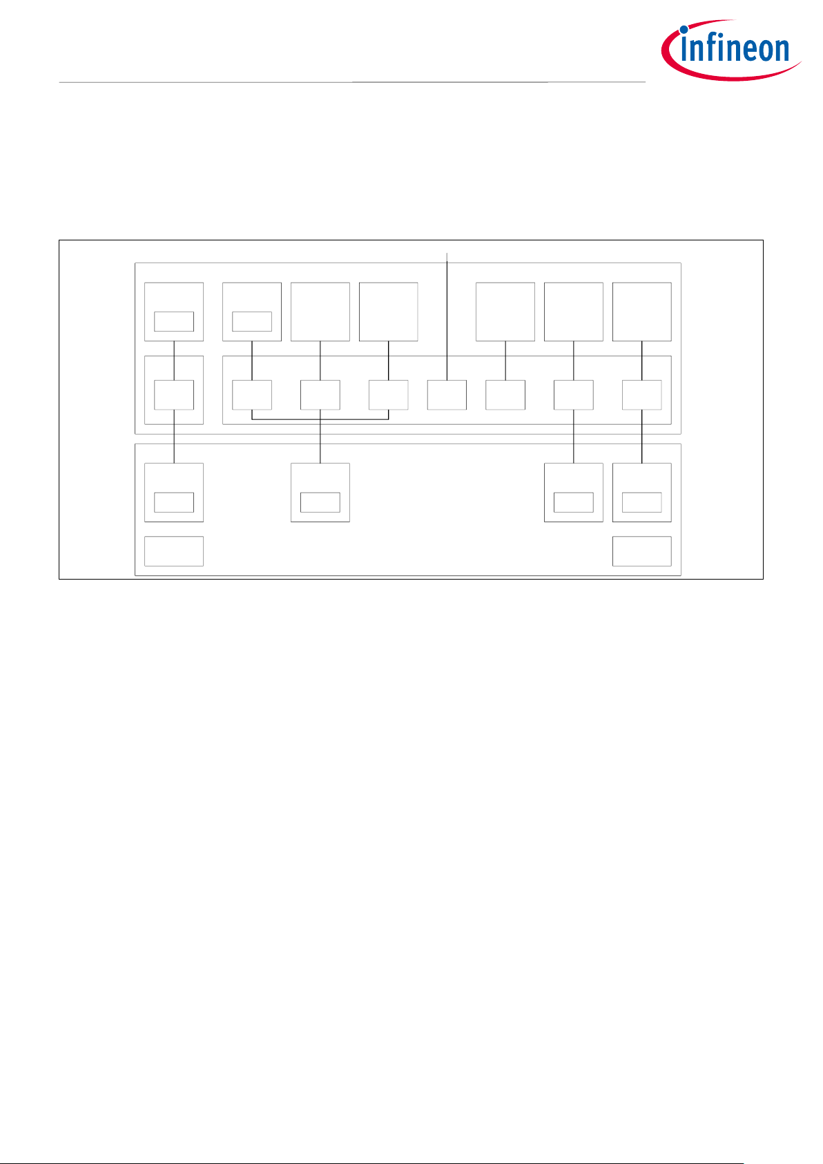
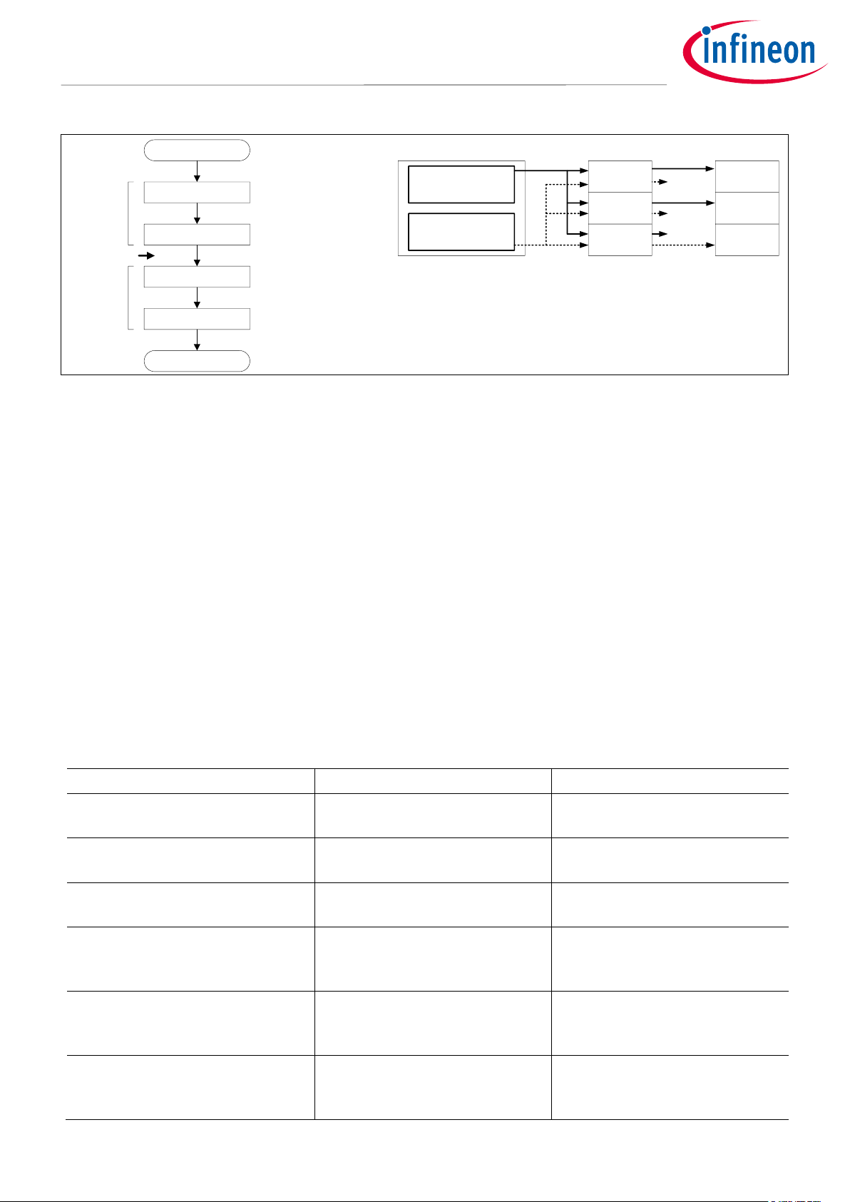
2 Protection Units
2.1 Location of Protection Units
Figure 1 shows the locations of MPUs, SMPUs, and PPUs in the CYT2B series.
m4cpuss
Peripheral Block
fast_infra slow_infra
CM4 CPU
MPU
SMPU
CM0+ CPU
MPU
SMPU
CRYPTO
SMPU
P-DMA 0 P-DMA 1
SMPU
Master
Interface
PPU
Peripheral
Group 0
SMPU
Master
Interface
PPU
Master
Interface
PPU
Master
Interface
PPU
SMPU/
MPU
Slow external masters
Test
Controller
SMPU/
MPU
M-DMA
SMPU
Peripheral
Group 15
Figure 1 Protection Unit Locations in the CYT2B Series
See the Architecture TRM for other series location.
2.2 Protection Units Overview
MPUs are associated with a single master. There are following two types of MPUs.
• An MPU that is implemented as part of the CPU: This type is found in the Arm CPUs.
• An MPU that is implemented as part of the bus infrastructure: This type is found in bus masters such as test
controller.
However, Peripheral DMA (P-DMA 0/1), Memory DMA (M-DMA), and Cryptography (CRYPTO) component do not
have an MPU. These masters inherit the access control attributes of the bus transfer that programmed channels
or components.
An SMPU is shared by all bus masters. A single set of SMPU region structures provides the same protection
information to all SMPUs in the systems.
A PPU is shared by all bus masters. PPU provides access control to the peripherals within a peripheral group.
There are the following two types of PPU:
• Fixed PPU: The address to protect is fixed and cannot be modified by software.
• Programmable PPU: The address to protect is programmable by software.
MPU and SMPU have a higher priority over PPU. In addition, programmable PPU has a higher priority than fixed
PPU.
See the Architecture TRM for more details on protection units.
Page 5
5 of 49 002-19843 Rev.*E
<2021-02>
Protection Configuration in Traveo II
Operation Overview
3 Operation Overview
3.1 Protection Properties of Bus Transfer
Protection units identify the following properties of bus transfer:
• An address range to be accessed
• Access attributes such as the following:
− Read/Write: Distinguish a read access from a write access
− Execute: Distinguish a code access from a data access
− User/Privileged: Distinguish a user access from a privileged access
− Secure/non-secure: Distinguish a "secure" code access from a "non-secure" code access. The non-secure
attribute allows both non-secure and secure accesses.
− Protection context: Distinguish accesses from different protection contexts
Not all bus masters provide all these access attributes. No bus master has a protected context; Arm CPUs do
not have a secure attribute.
Access attributes not provided by the bus master are provided by the PROT_MPUx_MS_CTL and
PROT_SMPU_MSx_CTL registers. These registers may be set during the boot process or by the secure CPU.
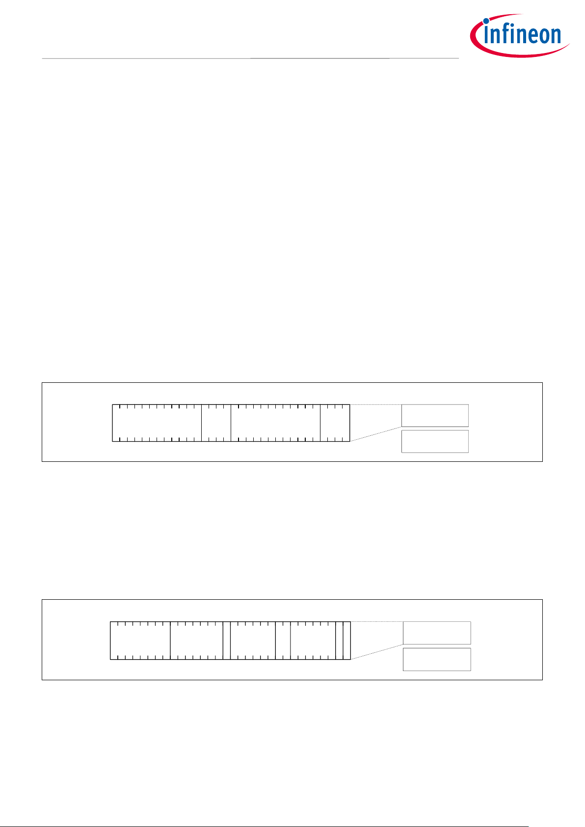
Figure 2 shows the structure of PROT_MPUx_MS_CTL registers.
PROT_MPUx_MS_CTL
0
31
PC[3:0]
Master Control 0
PC_SAVED
[19:16]
Master Control 1
...
Figure 2 PROT_MPUx_MS_CTL Register
This register grants a protection context attribute to its master access.
• PROT_MPUx_MS_CTL.PC: Sets the protection context attribute of its own access
• PROT_MPUx_MS_CTL.PC_SAVED: The boot process sets this field. This field is only present for the CM0+
master.
Figure 1 shows the structure of the PROT_SMPU_MSx_CTL registers.
PROT_SMPU_MSx_CTL
0
31
Master Control 0
PC_MASK
_15_TO_1
[23:17]
Master Control 1
...
P
NS
PRIO
[9:8]
PC_MASK_0
Figure 3 Figure 1. PROT_SMPU_MSx_CTL Register
This register grants a following attributes to its master access.
• PROT_SMPU_MSx_CTL.P: Provides the User/Privileged attribute for masters that do not provide their own
attribute.
Page 6

6 of 49 002-19843 Rev.*E
<2021-02>
Protection Configuration in Traveo II
Operation Overview
• PROT_SMPU_MSx_CTL.NS: Provides the Secure/Non-Secure attribute for masters that do not provide their
own attributes.
• PROT_SMPU_MSx_CTL.PC_MASK_15_TO_1 and PC_MASK_0: Restricts the protection context that the bus
master can set to MPUx_MS_CTL.PC.
• The PC_MASK_0 field is always ‘0’. This means that bus masters cannot set the PC = 0 attribute.
• PROT_SMPU_MSx_CTL.PRIO: Sets the bus arbitration priority.
However, not all bus masters have these register fields. Table 1 shows the relationship of registers for each
master.
Table 1 Register Field Provided to the Master
Register Field
CM0+ CPU
CRYPTO
Component
P-DMA 0
P-DMA 1
M-DMA
CM4F CPU
Test
Controller
PROT_MPUx_MS_
CTL.PC
Yes – – – –
Yes
Yes
PROT_MPUx_MS_
CTL.PC_SAVED
Yes – – – – – –
PROT_SMPU_MSx_
CTL.P
– – – – – – Yes
PROT_SMPU_MSx_
CTL.NS
Yes – – – –
Yes
Yes
PROT_SMPU_MSx_
CTL.PC_MASK_15_T
O_1 and
PC_MASK_0
Yes – – – –
Yes
Yes
PROT_SMPU_MSx_
CTL.PRIO
Yes
Yes
Yes
Yes
Yes
Yes
Yes
P-DMA0/1, M-DMA, and CRYPTO components do not have MPU. Therefore, these peripheral functions do not
have fields to set attributes.
Each master has an associated SMPU MS_CTL register. However, in secure systems, this register can be
typically controlled only by the secure master (CM0+) to prevent a master from changing its own privileged
setting, security setting, arbitration priority, or enabled protection contexts.
3.2 Attribute Inheritance
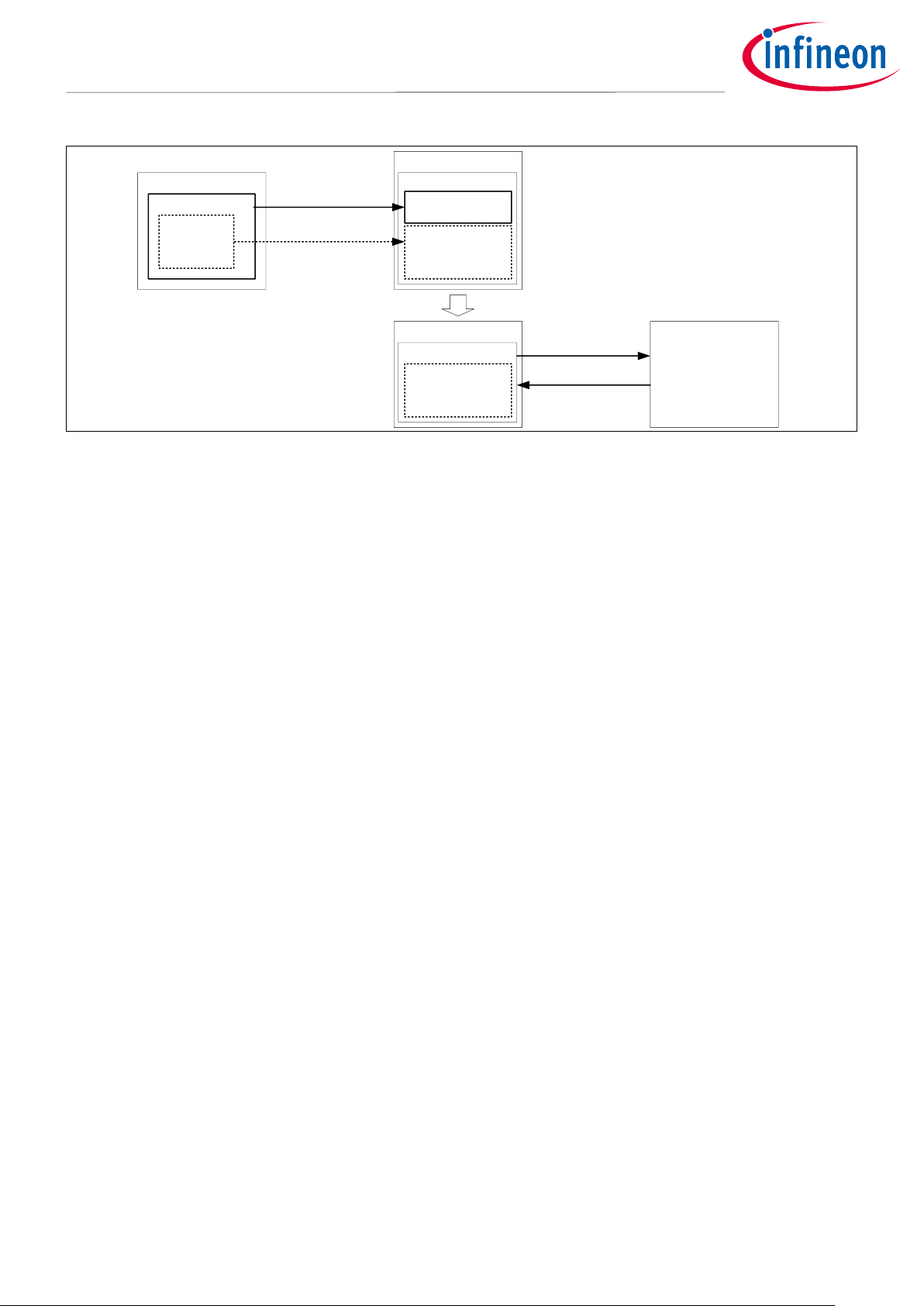
As mentioned earlier, P-DMA, M-DMA, and CRYPTO components inherit the access control attributes of the bus
transfers that programmed the channels and component. The inherited access attribute is allowed/restricted
by SMPU and PPU.
Figure 4 shows examples of the setting and behavior for inheriting attributes.
Page 7
7 of 49 002-19843 Rev.*E
<2021-02>
Protection Configuration in Traveo II
Operation Overview
CPU
Channel Setting Task
Task Attribute
- User
- Non-Secure
- PC=7
P-DMA
Configuration
Register
Channel Attribute
- User
- Non-Secure
- PC=7
Channel A
Channel Setting
Inherit Access Attributes
P-DMA
Channel Attribute
- User
- Non-Secure
- PC=7
Channel A
Memory or Peripheral
User Write,
Non-Secure, PC=7
User Read,
Non-Secure, PC=7
Figure 4 Setting and Behavior Example for Attribute Inheritance
3.3 User/Privileged Attribute Switching
This section describes attribute switching of both CPUs supporting User/Privileged attributes. CPUs support
two operating modes and two privilege levels as follows:
• Operation Mode
− Thread Mode: This mode is used to execute application software. This mode can run in Privileged level or
User level.
− Handler Mode: This mode is used to handle exceptions. This mode only runs in Privileged level.
• Privileged Levels
− User Level: The software has limited access
− Privileged Level: The software can use all instructions and access all resources
Privileged level is switched by the CONTROL register. It is a CPU-specific register. Switching from Privileged
level to User level is performed by the CONTROL register. However, the CONTROL register can be rewritten only
with the privileged level. Therefore, switching from the User level to the Privileged level must always go
through the Handler mode. The CPU enters the Handler mode when an exception or interrupt occurs. Figure 5
shows an example User/Privileged level switching by the SVC (Supervisor call) instruction exception. The SVC
instruction generates an exception and can enter the Handler mode.
Page 8
8 of 49 002-19843 Rev.*E
<2021-02>
Protection Configuration in Traveo II
Operation Overview
Handler/Privileged Thread/Privileged Thread/User
Reset Relese
(1) Operation
(2) Operation (2) Operation
(3) Change CONTROL
= Unprivileged
(3) Operation
(4) Operation (4) Operation
(5) Operation
(6) Change CONTROL
= Privileged
(6) Operation
(5) SVC
2) Exception
(4) Exception
(5) SVC Exception
Figure 5 Example User/Privileged Level Switching for Both CPUs
1. CPUs are started in Thread/Privileged mode after reset release.
2. When an exception occurs in Thread/Privileged mode, the Handler/Privileged mode is entered, and upon
return from handler processing, Thread/Privileged mode is entered again.
3. In the Thread/Privileged mode, transition to the Thread/User mode is allowed by the CONTROL register.
4. When an exception occurs in the Thread/User mode, the Handler/Privileged mode is entered, and upon
return from handler processing, Thread/User mode is entered again.
5. When switching from the Thread/User mode to Thread/Privileged mode, use SVC instruction to enter the
Handler/Privileged mode. The SVC instruction can cause an SVC exception.
6. Set the Privileged level with the CONTROL register in the Handler/Privileged level. The CPU transitions to
the Thread/Privileged mode after returning from handler processing.
See the Arm documentation sets for CM4, CM7, and CM0+ for more details.
You need to register the SVC handler in advance.
3.3.1 User/Privileged Attribute Switching Procedure
This section explains how to switch between Privileged and User modes.
3.3.2 Configuration
Table 2 lists the functions in SDL for User/Privileged attribute switching using SVC instruction.
Table 2 List of Functions
Functions
Description
Remarks
GetUserMode()
Change Privileged Level to User
-
GetPrivilegedMode()
Change Privileged Level to
Privileged
-
SVC_GetPrivilegedMode()
Generates SVC interrupt.
-
Cy_SysLib_SvcHandler(pSvcArgs)
SVC handler
pSvcArgs: SVC Index
Change to Privileged if index is
“2”
Page 9
9 of 49 002-19843 Rev.*E
<2021-02>
Protection Configuration in Traveo II
Operation Overview
The following code shows an example of switching using SVC.
Code Listing 1 Example of User/Privileged Switching using SVC
int main(void)
{
SystemInit();
__enable_irq();
:
/* Get user mode from here */
GetUserMode();
:
/* Access privileged write only port register after getting privileged mode */
SVC_GetPrivilegedMode();
:
/* Access privileged write only port register after getting user mode */
GetUserMode();
:
for(;;);
}
Code Listing 2 GetUserMode() Function
void GetUserMode(void)
{
__ASM("MRS r0, CONTROL"); // Read CONTROL register into R0
__ASM("ORR r0, r0, #1"); // nPRIV -> 1
__ASM("MSR CONTROL, r0"); // Write R0 into CONTROL register
}
Code Listing 3 SVC_GetPrivilegedMode()
void SVC_GetPrivilegedMode(void)
{
__ASM("SVC 0x02"); // SVC index = 2: Get privileged mode
}
Change Privileged Mode to User Mode.
See Code Listing 2.
Change from User Mode to Privileged Mode.
See Code Listing 3.
Change from Privileged Mode to User Mode.
See Code Listing 2.
Read CONTROL Register
Write back to CONTROL Register
(3) Change to User Mode
(5) SVC Exception with Index 2. It calls the SVC handler.
See Code Listing 4.
CPUs are started in Thread/Privileged mode
after reset release.
Set Index to “2”
Page 10
10 of 49 002-19843 Rev.*E
<2021-02>
Protection Configuration in Traveo II
Operation Overview
Code Listing 4 SVC Handler
void Cy_SysLib_SvcHandler(uint32_t* pSvcArgs)
{
uint8_t svcIdx = ((char*)pSvcArgs[6])[-2];
switch(svcIdx)
{
case 0:
:
break;
case 1:
:
break;
case 2:
GetPrivilegedMode();
break;
default:
break;
}
}
Code Listing 5 GetPrivilegedMode() Function
void GetPrivilegedMode(void)
{
__ASM("MRS r0, CONTROL"); // Read CONTROL register into R0
__ASM("BIC r0, r0, #1"); // nPRIV -> 0
__ASM("MSR CONTROL, r0"); // Write R0 into CONTROL register
}
3.4 Protection Context Attribute Setting
Protection Contexts (PCs) are used to isolate software execution for security and safety purposes. PCs are used
as the PC attribute for all bus transfers that are initiated by the master. SMPUs and PPUs allow or restrict bus
transfers based on the PC attribute.
The series supports eight PCs. Protection contexts 0 and 1 out of eight PCs are special; these are controlled by
hardware. In addition, PC0 has unrestricted access.
Specific bus masters have associated PC fields (PROT_MPUx_MS_CTL.PC and
PROT_SMPU_MSx_CTL.PC_MASK_15_TO_1 and PC_MASK_0).
A bus master protection context is changed by reprogramming the associated PROT_MPUx_MS_CTL.PC field.
The PROT_SMPU_MSx_CTL.PC_MASK field restricts the PCs that can be set for the associated bus master.
For example, if PROT_SMPU_MSx_CTL.PC_MASK[15:0] = “0x06” (PC1, 2 = "1"), the PCs to which the associated
bus master can be set are “PC = 1” and “PC = 2”. A bus master cannot be changed to a PC not allowed
(PC=0,3,4,5,6,7).
Figure 6 shows an example of changing the flow of PCs.
SVC Processing for Index 0.
SVC Processing for Index 1.
SVC Processing for Index 2. Change to Privileged Mode.
See Code Listing 5.
Read CONTROL Register
Write back to CONTROL Register
(6) Change to Privileged Mode
Page 11
11 of 49 002-19843 Rev.*E
<2021-02>
Protection Configuration in Traveo II
Operation Overview
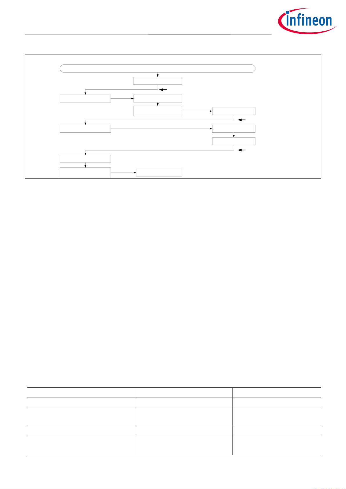
Start
(1) Change PC
TASK A processing
(2) Change PC
TASK B processing
Start
Task switch
Task A
Task B
PC = 4
All bus transfers initiated by
the master are accessed as
PC = 4.
PC = 5
All bus transfers initiated by
the master are accessed as
PC = 5.
Task A (PC=4)
Task B (PC=5)
CPU SMPU
Region 0
Region 1
Region 2
Memory
Task B is
Not-allowed
Task B is
Not-allowed
Task A is
Not-allowed
Region 0
PC = 4
Region 1
PC = 4
Region 2
PC = 5
Figure 6 Change Flow of PCs and Behavior
Note: PC values that can be set by each master are restricted by
PROT_SMPU_MSx_CTL.PC_MASK_15_TO_1 and PC_MASK_0.
This allows a single bus master to take on different protection roles by reprogramming only the protection
context field without changing the settings of SMPUs and PPUs.
3.4.1 Protection Context Attribute Switching Procedure
This section explains how to switch protection context shown in Figure 6.
• Region 0 and 1: PC=4 access has permissions
• Region 2: PC=5 access has permissions
3.4.2 Configuration
Table 3 and Table 4 list the parameters and functions in SDL for protection context switching.
Table 3 List of Parameters
Parameters
Description
Value
RESERVED_MEMORY_BLOCK_SIZE
Define Memory size of each
region
0x400
PROTECTION_CONTEXT_OF_TASK_
A
Define Protection Context
number for TASK A
4u
PROTECTION_CONTEXT_OF_TASK_
B
Define Protection Context
number for TASK B
5u
PC_MASK_OF_TASK_A
Define
PROT_SMPU_MSx_CTL.PC_MASK
value for enabling PC=4.
-
PC_MASK_OF_TASK_B
Define
PROT_SMPU_MSx_CTL.PC_MASK
value for enabling PC=5.
-
gReservedRam.taskA_Region0/1/2
Set start address and memory
size of Region 0/1/2
Memory size =
RESERVED_MEMORY_BLOCK_SIZ
E
Page 12

12 of 49 002-19843 Rev.*E
<2021-02>
Protection Configuration in Traveo II
Operation Overview
Parameters
Description
Value
gSmpuStructConfigOfTask(A/B).
address
Set SMPU region (Base Address)
gReservedRam.taskA_Region0/1/
2
gSmpuStructConfigOfTask(A/B).
regionSize
Set SMPU region (Region Size)
CY_PROT_SIZE_1KB (1KB)
gSmpuStructConfigOfTask(A/B).
subregions
Set SMPU region (Subregion
setting)
0x00u (Not used)
gSmpuStructConfigOfTask(A/B).
userPermission
Set SMPU region (User
Permission setting)
CY_PROT_PERM_RWX (=0x07u)
Full access for User
gSmpuStructConfigOfTask(A/B).
privPermission
Set SMPU region (Privileged
Permission setting)
CY_PROT_PERM_RWX (=0x07u)
Full access for Privileged
gSmpuStructConfigOfTask(A/B).
secure
Set SMPU region (Non-Secure
setting)
False (Non-Secure)
gSmpuStructConfigOfTask(A/B).
pcMatch
Set SMPU region (PC Match
setting)
False (PC field participates in
"matching")
gSmpuStructConfigOfTask(A/B).
pcMask
Set SMPU region (PC_MASK
setting)
Region 0/1:
PC_MASK_OF_TASK_A
Region 2: PC_MASK_OF_TASK_B
PROT_SMPU_SMPU_STRUCT0/1/2
Define Base address of
PROT_SMPU_SMPU_STRUCT0/1/
2
It depends on the product. See
Registers TRM.
-
CPUSS_MS_ID_CM4
Define Bus muster Identifiers.
It depends on the product. See
Master Identifier.
14
Table 4 List of Functions
Functions
Description
Value
Cy_Prot_ConfigBusMaster
(busMaster, privileged,
secure, pcmask)
PROT_PROT_SMPU_MSx_CT
L setting
busMaster: Bus muster
Identifiers
privileged; P field setting
secure: NS filed setting
pcmask: PC_MASK field
setting
See Registers TRM.
busMaster: CPUSS_MS_ID_CM4
privileged; true (User mode)
secure: false (Non-Secure)
pcmask: PC_MASK field setting
Cy_Prot_ConfigSmpuSlaveStruct
(*base, *config)
SMPU Region setting
*base: Register Base address
*config: Configuration
parameter
*base:
PROT_SMPU_SMPU_STRUCT0/1/2
*config:
gSmpuStructConfigOfTask(A/B)
Cy_Prot_EnableSmpuSlaveStruct
(*base)
SMPU Region enable
*base: Register Base address
*base:
PROT_SMPU_SMPU_STRUCT0/1/2
Page 13
13 of 49 002-19843 Rev.*E
<2021-02>
Protection Configuration in Traveo II
Operation Overview
Functions
Description
Value
Cy_Prot_SetActivePC(busMaster
, PC)
PROT_MPU_MSx_CTL setting
busMaster: Bus muster
Identifiers
PC: PC value
busMaster: CPUSS_MS_ID_CM4
PC:
PROTECTION_CONTEXT_OF_TASK_
A or
PROTECTION_CONTEXT_OF_TASK_
B
The following description will help you understand the register notation of the driver part of SDL:
• addrMpu->unMS_CTL.u32Register is the PROT_MPUx_MS_CTL register mentioned in the Registers TRM.
Other registers are also described in the same manner. “x” signifies the bus master Identifiers.
• Performance improvement measures
• For register setting performance improvement, the SDL writes a complete 32-bit data to the register. Each
bit field is generated in advance in a bit writable buffer and written to the register as the final 32-bit data.
tempSL_ATT0.u32Register = base->unSL_ATT0.u32Register;
tempSL_ATT0.stcField.u1PC1_UR = (config->userPermission & CY_PROT_PERM_R);
tempSL_ATT0.stcField.u1PC1_UW = (config->userPermission & CY_PROT_PERM_W) >> 1;
tempSL_ATT0.stcField.u1PC1_PR = (config->privPermission & CY_PROT_PERM_R);
tempSL_ATT0.stcField.u1PC1_PW = (config->privPermission & CY_PROT_PERM_W) >> 1;
tempSL_ATT0.stcField.u1PC1_NS = !(config->secure);
base->unSL_ATT0.u32Register = tempSL_ATT0.u32Register;
See cyip_prot_v2.h and cyip_peri_ms_v2.h under hdr/rev_x/ip for more information on the union and structure
representation of registers.
Code Listing 6 shows an example of switching protection context.
Code Listing 6 Example of User/Privileged Switching Protection Context
#define RESERVED_MEMORY_BLOCK_SIZE (0x400) // 1K
#define PROTECTION_CONTEXT_OF_TASK_A (4u)
#define PROTECTION_CONTEXT_OF_TASK_B (5u)
#define PC_MASK_OF_TASK_A (1u<<(PROTECTION_CONTEXT_OF_TASK_A-1u))
#define PC_MASK_OF_TASK_B (1u<<(PROTECTION_CONTEXT_OF_TASK_B-1u))
struct
{
uint8_t taskA_Region0[RESERVED_MEMORY_BLOCK_SIZE];
uint8_t taskA_Region1[RESERVED_MEMORY_BLOCK_SIZE];
uint8_t taskB_Region2[RESERVED_MEMORY_BLOCK_SIZE];
} gReservedRam;
cy_stc_smpu_cfg_t gSmpuStructConfigOfTaskA =
{
.address = NULL, // Will be updated in run time
.regionSize = CY_PROT_SIZE_1KB,
.subregions = 0x00u,
.userPermission = CY_PROT_PERM_RWX,
.privPermission = CY_PROT_PERM_RWX,
.secure = false, // Non secure
.pcMatch = false,
.pcMask = PC_MASK_OF_TASK_A, // only enable for task A
};
Define each region size
Define Protection context for Task A (PC=4)
Define Protection context for Task B (PC=5)
Define PC_Mask for each SMPU
region.
Define SRAM region.
Configure SMPU for region 0
and 1.
(PC=4 access has permissions)
Page 14
14 of 49 002-19843 Rev.*E
<2021-02>
Protection Configuration in Traveo II
Operation Overview
cy_stc_smpu_cfg_t gSmpuStructConfigOfTaskB =
{
.address = NULL, // Will be updated in run time
.regionSize = CY_PROT_SIZE_1KB,
.subregions = 0x00u,
.userPermission = CY_PROT_PERM_RWX,
.privPermission = CY_PROT_PERM_RWX,
.secure = false, // Non secure
.pcMatch = false,
.pcMask = PC_MASK_OF_TASK_B, // only enable for task B
};
int main(void)
{
SystemInit();
cy_en_prot_status_t status;
/* Setting for MS14_CTL (for CM4) to allow the PC value to become 4 or 5 */
status = Cy_Prot_ConfigBusMaster(CPUSS_MS_ID_CM4, true, false, (PC_MASK_OF_TASK_A|PC_MASK_OF_TASK_B));
CY_ASSERT(status == CY_PROT_SUCCESS);
/* Setting for SMPU_STRUCT 0 */
/* Setting SMPU_STRUCT 0 for task A */
gSmpuStructConfigOfTaskA.address = (uint32_t*)gReservedRam.taskA_Region0;
status = Cy_Prot_ConfigSmpuSlaveStruct(PROT_SMPU_SMPU_STRUCT0, &gSmpuStructConfigOfTaskA);
CY_ASSERT(status == CY_PROT_SUCCESS);
/* Enable SMPU_STRUCT 0 */
status = Cy_Prot_EnableSmpuSlaveStruct(PROT_SMPU_SMPU_STRUCT0);
CY_ASSERT(status == CY_PROT_SUCCESS);
/* Setting for SMPU_STRUCT 1 */
/* Setting SMPU_STRUCT 1 for task A */
gSmpuStructConfigOfTaskA.address = (uint32_t*)gReservedRam.taskA_Region1;
status = Cy_Prot_ConfigSmpuSlaveStruct(PROT_SMPU_SMPU_STRUCT1, &gSmpuStructConfigOfTaskA);
CY_ASSERT(status == CY_PROT_SUCCESS);
/* Enable SMPU_STRUCT 1 */
status = Cy_Prot_EnableSmpuSlaveStruct(PROT_SMPU_SMPU_STRUCT1);
CY_ASSERT(status == CY_PROT_SUCCESS);
/* Setting for SMPU_STRUCT 2 */
/* Setting SMPU_STRUCT 2 for task B */
gSmpuStructConfigOfTaskB.address = (uint32_t*)gReservedRam.taskB_Region2;
status = Cy_Prot_ConfigSmpuSlaveStruct(PROT_SMPU_SMPU_STRUCT2, &gSmpuStructConfigOfTaskB);
CY_ASSERT(status == CY_PROT_SUCCESS);
/* Enable SMPU_STRUCT 2 */
status = Cy_Prot_EnableSmpuSlaveStruct(PROT_SMPU_SMPU_STRUCT2);
CY_ASSERT(status == CY_PROT_SUCCESS);
for(;;)
{
/* Setting for MPU so that CM4 PC for task A */
status = Cy_Prot_SetActivePC(CPUSS_MS_ID_CM4, PROTECTION_CONTEXT_OF_TASK_A);
CY_ASSERT(status == CY_PROT_SUCCESS);
/* Do task A */
Routine_TaskA();
/* Setting for MPU so that CM4 PC for task B */
status = Cy_Prot_SetActivePC(CPUSS_MS_ID_CM4, PROTECTION_CONTEXT_OF_TASK_B);
CY_ASSERT(status == CY_PROT_SUCCESS);
/* Do task B */
Routine_TaskB();
}
}
Note: (*)This process specifies the value of the protection context that can be set by the corresponding
master. In a secure system, it is run by secure master. See Protection Properties of Bus Transfer for
more details.
Enabled PC=5 by PC_MASK
Configure SMPU for region 2.
(PC=5 access has permissions)
Set PROT_SMPU_MS14_CTL.PC_MASK. See Configuration
Example of SMPU for SMPU setting details. (*)
Set SMPU region
0. For details on
setting SMPU,
see
Configuration
Example of
SMPU.
Enable SMPU region 0. For details on setting SMPU,
see Configuration Example of SMPU.
(1) Change protection context to PC=4
for TASK A. See 0.
(2) Change protection context to PC=5
for TASK B. See 0.
Access to RAM region 0 and 1.
See Code Listing 8.
Access to RAM region 2.
See Code Listing 8.
Set SMPU region 1.
For details on
setting SMPU, see
Configuration
Example of SMPU.
Enable SMPU region 1. For details on setting
SMPU, see Configuration Example of SMPU.
Set SMPU
region 2. For
details on
setting SMPU,
see
Configuration
Example of
Enable SMPU region 1. For details on setting
SMPU, see Configuration Example of SMPU.
Page 15
15 of 49 002-19843 Rev.*E
<2021-02>
Protection Configuration in Traveo II
Operation Overview
Code Listing 7 Cy_Prot_SetActivePC() Function
cy_en_prot_status_t Cy_Prot_SetActivePC(en_prot_master_t busMaster, uint32_t pc)
{
cy_en_prot_status_t status = CY_PROT_SUCCESS;
un_PROT_MPU_MS_CTL_t tProtMpuMsCtl = {0ul};
volatile stc_PROT_MPU_t* addrMpu = (stc_PROT_MPU_t*)(&PROT->CYMPU[busMaster]);
if(pc > (uint32_t)CY_PROT_MS_PC_NR_MAX)
{
/* Invalid PC value - not supported in device */
status = CY_PROT_BAD_PARAM;
}
else
{
tProtMpuMsCtl.stcField.u4PC = pc;
addrMpu->unMS_CTL.u32Register = tProtMpuMsCtl.u32Register;
status = ((addrMpu->unMS_CTL.stcField.u4PC != pc) ? CY_PROT_FAILURE : CY_PROT_SUCCESS);
}
return status;
}
Code Listing 8 Routine_TaskA() and Routine_TaskB() Function
void Routine_TaskA(void)
{
for(uint32_t i = 0; i < RESERVED_MEMORY_BLOCK_SIZE; i++)
{
gReservedRam.taskA_Region0[i] += 1;
}
for(uint32_t i = 0; i < RESERVED_MEMORY_BLOCK_SIZE; i++)
{
gReservedRam.taskA_Region1[i] += 1;
}
}
void Routine_TaskB(void)
{
for(uint32_t i = 0; i < RESERVED_MEMORY_BLOCK_SIZE; i++)
{
gReservedRam.taskB_Region2[i] += 1;
}
}
3.5 Bus Transfer Evaluation
3.5.1 Evaluation Process
The evaluation of bus transfer by protection units is divided into two independent processes.
• Matching process: For each protection structure, this process determines whether a transfer address is
contained within the address range.
• Access evaluation process: For each protection structure, this process evaluates the bus transfer access
attributes against the access control attributes.
The following pseudo code shows the evaluation process of bus transfer.
match = 0;
for (i = n-1; i >= 0; i--) // n: number of protection regions
if (Match (“transfer address”, “protection context”) {
match = 1; break;
}
if (match)
AccessEvaluate (“access attributes”, “protection context”);
else
“access allowed”
Matching Process
Access Evaluation Process
Access to region 0 and 1 with TASK A.
If these regions are accessed with TASK B,
it will cause bus fault.
Access to region 2 with TASK B.
If these regions are accessed with TASK A,
it will cause bus fault.
Check protection context value, if available.
Change protection context.
Page 16

16 of 49 002-19843 Rev.*E
<2021-02>
Protection Configuration in Traveo II
Operation Overview
Note: If no protection structure provides a match, access is allowed.
Note: If multiple protection structures provide a match, the access control attributes for access
evaluation are provided by the protection structure with the highest index.
A protection unit evaluates the protection structures in the decreasing order. In other words, higher-indexed
structures take precedence over lower-indexed structures.
When transfer addresses do not match, the protection structure with the next highest index is evaluated. When
transfer addresses match, bus transfer access attributes are evaluated by the access evaluation process. If
transfer access attributes do not match with the access evaluation process, it is detected as an access violation.
Therefore, the protection structure with the next highest index is not evaluated.
3.5.2 PC_MATCH Operation
SMPU has a PC_MATCH field. PC_MATCH controls "matching" and "access evaluation" processes.
• Case of PC_MATCH = 0
The following pseudo code shows the evaluation process when PC_MATCH = 0.
match = 0;
for (i = n-1; i >= 0; i--) // n: number of protection regions
if (Match (“transfer address”) {
match = 1; break;
}
if (match)
AccessEvaluate (“access attributes”, “protection context”);
else
“access allowed”
When PC_MATCH = “0”, Protection context is evaluated only in the access evaluation process.
Figure 7 shows the operation example when PC_MATCH of Region5 is ‘0’ and PC_MATCH of Region4 is ‘0’.
Table 5 shows the settings for each region.
Table 5 Region Setting1 for PC_MATCH Operation
Region
PC_MATCH
Region Address
Protection Context
User
Region4
0
AA 4 Read/Write
Region5
0
AA 5 Read only
Region5
- PC_MATCH = 0
- ADDR = AA
- PC = 5
- USER = Read-Only
- Privileged = Read/Write
Region4
- PC_MATCH = 0
- ADDR = AA
- PC = 4
- USER = Read/Write
- Privileged = Read/Write
PC = 5, ADDR = AA,
Privileged Read
Matching Process
Without PC: Match
Access Evaluation Process:
Match
Access Allowed
PC = 4, ADDR = AA,
User Read
Matching Process
Without PC: Match
Access Evaluation Process:
Not Matched
Access Prohibited
Memory
ADDR = AA
SMPU
Page 17

17 of 49 002-19843 Rev.*E
<2021-02>
Protection Configuration in Traveo II
Operation Overview
Figure 7 PC_MATCH Operation Example1
In this case, the protection Context is not evaluated by the matching process. Therefore, both PC = 4 access and
PC = 5 access is "match" in the matching process. The Protection Context is evaluated by the access evaluation
process. For PC = 5, access is allowed; for PC = 4, access is not allowed. As a result, PC = 4 access cannot access
this address because PC = 4 access is prohibited by Region5 with a higher priority than Region4.
• Case of PC_MATCH = 1
The following pseudo code shows the evaluation process when PC_MATCH = 1.
match = 0;
for (i = n-1; i >= 0; i--) // n: number of protection regions
if (Match (“transfer address”, “protection context”) {
match = 1; break;
}
if (match)
AccessEvaluate (“access attributes”, “protection context”);
else
“access allowed”
When PC_MATCH = "1", the protection context is evaluated not only by the access evaluation process, but also
by the matching process.
Figure 8 shows the operation example when PC_MATCH of Region5 is ’1’ and PC_MATCH of Region4 is ‘0’.
Table 6 shows the settings for each region.
Table 6 Region Setting2 for PC_MATCH Operation
Region
PC_MATCH
Region Address
Protection Context
User
Region4
0
AA 4 Read/Write
Region5
1
AA 5 Read only
PC = 5, ADDR = AA,
Privileged Read
Matching Process with PC:
Match
Access Evaluation Process:
Match
Access Allowed
PC = 4, ADDR = AA,
User Read
Matching Process with PC:
Not Matched
Access Evaluation Process
Matching Process:
Match
Access Evaluation Process:
Match
Access Allowed
Region5
- PC_MATCH = 1
- ADDR = AA
- PC = 5
- USER = Read Only
- Privileged = Read/Write
Region4
- PC_MATCH = 0
- ADDR = AA
- PC = 4
- USER = Read/Write
- Privileged = Read/Write
Memory
ADDR = AA
SMPU
Figure 8 PC_MATCH Operation Example2
In this case, the Protection Context is also evaluated by the matching process. PC = 5 access is "match" in the
matching process, and is evaluated by the access evaluation process. However, PC = 4 access is "Not matched",
and is evaluated by the matching process with Region4 of the next highest priority. It is evaluated by the access
evaluation process after the matching process, and access is allowed.
Page 18

18 of 49 002-19843 Rev.*E
<2021-02>
Protection Configuration in Traveo II
Operation Overview
It is possible to assign different attributes to the same address area depending on the Protection Context by
using PC_MATCH.
Note : PC_MATCH is provided only for the SMPU. This functionality is not supported because a PPU
structure provides access attributes for all protection contexts.
3.6 Master Identifier
Each bus master has a dedicated master identifier. This identifier is used for correspondence with the register
suffix in protection units and identification of access violation master by protection units. Table 7 lists the
master identifiers. See the related datasheet for bus master identifier using products.
Table 7 Master Identifiers
Master
identifier
Bus Master
CYT2B7 series
CYT4BF series
CYT4DN series
0
CM0+ CPU
CM0+ CPU
CM0+ CPU
1
CRYPTO Component
CRYPTO Component
CRYPTO Component
2
P-DMA 0
P-DMA 0
P-DMA 0
3
P-DMA 1
P-DMA 1
P-DMA 1
4
M-DMA
M-DMA
M-DMA
5 - SDHC
- 9 -
Ethernet 0
Ethernet 0
10 - Ethernet 1
-
12 - -
Video Subsystem
13 - CM7_1 CPU
CM7_1 CPU
14
CM4 CPU
CM7_0 CPU
CM7_0 CPU
15
Test Controller
Test Controller
Test Controller
3.7 Protection Violation
If the MPU that is implemented as part of the CPU detected access violations, invoke the programmablepriority MemManage fault or HardFault handler. If an MPU fault occurs on an access that is not in the TCM, the
AXI or AHB transactions for that access are not performed. See the Arm documentation sets for CM4, CM7, and
CM0+ for more MPU details.
If the MPU that is implemented as part of the bus infrastructure and SMPU detects a bus transfer that causes a
violation of the protection status, the bus transfer results in a bus error.
In case of write transfers that violate PPU protection, the bus master will not see the bus error when buffering is
enabled (CPUSS_BUFF_CTL.WRITE_BUFF = 1). This is because AHB-Lite bridges in the bus infrastructure will
buffer the write transfer and send the OK response to masters. In this case, the system must depend on the
fault reported by the PPU. Write transfers that violate the PPU cause a bus error if buffering is disabled
(CPUSS_BUFF_CTL.WRITE_BUFF = 0). Read transfers that violate PPU protection always result in a bus error.
The bus transfers that violate protection units do not reach their target memory location or peripheral register.
Protection violation detected by the MPU that is implemented as part of the bus infrastructure, SMPU, and PPU
is captured in the fault report structure. The fault report structure can generate an interrupt to indicate the
Page 19

19 of 49 002-19843 Rev.*E
<2021-02>
Protection Configuration in Traveo II
Operation Overview
occurrence of a fault. In addition, information on the violating bus transfer is communicated to the fault report
structure.
The fault reporting structure captures the following information:
• Violating Address
• Violating Attribute
− User Read/User Write/User Execute
− Privileged Read/Privileged Write/Privileged Execute
− Non-Secure
− Protection Context Identifier
• Violating Master Identifier
• Protection Units that detected the violation or fault type
1
1
Depends on the detected fault. See the Registers TRM.
Page 20

20 of 49 002-19843 Rev.*E
<2021-02>
Protection Configuration in Traveo II
Protection Units Structure
4 Protection Units Structure
4.1 MPU Structure
Figure 9 shows the MPU structure that is implemented as part of the bus infrastructure. See the Arm
documentation sets for CM4, CM7, and CM0+ for details of the MPU that is implemented as part of CM4, CM7,
and CM0+.
ATT
0
31
UR
UW
UX
PR
PW
PX
NS
ENABLED
REGION_
SIZE
[28:24]
ADDR
0
31
SUBREGION_
DISABL
[7;0]
ADDR24
[31:8]
MPU protection
structures
MPU protection
structure 0
...
MPU protection
structure 1
MPU protection
structure 2
Figure 9 MPU Structure
The MPU protection structure sets the property to be allowed and restricted by master access. An MPU
protection identifies the following properties:
• Address Range
− ADDR.ADDR24 [31:8]: Specifies the base address of the region
− ATT.REGION_SIZE [28:24]: Specifies the size of a region. The region size is in the range of [256 B, 4 GB]
− ADDR.SUBREGION_DISABLE [7:0]: Individual disable settings for eight subregions within the region
• Access Attribute
− ATT.UR: Control for User Read access
− ATT.UW: Control for User Write access
− ATT.UX: Control for User Execute access
− ATT.PR: Control for Privileged Read access
− ATT.PW: Control for Privileged Write access
− ATT.PX: Control for Privileged Execute access
− ATT.NS: Control for Secure access
• Region Enable
− ATT.ENABLED: Region Enable
The MPU does not provide a Protection Context. The definition of this MPU type follows the Arm MPU definition
(in terms of memory region and access attribute definition) to ensure a consistent software interface.
A region can be partitioned into eight equally sized subregions; it is possible to specify individual enables for
the subregions within a region with the ADDR.SUBREGION_DISABLE field.
For example, when SUBREGION_DISABLE is 0x82 (bit fields 1 and 7 are '1') in the divided subregion [0: 7],
subregion1, 7 are disabled, subregion 0, 2, 3, 4, 5, and 6 are enabled. Table 8 shows the areas of the eight
subregions and the Enable/Disable states if the start address is 0x10005400, and the region ranges from
0x10005400 to 0x100055ff (512 bytes).
Page 21

21 of 49 002-19843 Rev.*E
<2021-02>
Protection Configuration in Traveo II
Protection Units Structure
Table 8 Each Subregion Area and State
Subregion
Area
State
Subregion 0
0x10005400 to 0x1000543f
Enable
Subregion 1
0x10005440 to 0x1000547f
Disable
Subregion 2
0x10005480 to 0x100054bf
Enable
Subregion 3
0x100054c0 to 0x100054ff
Enable
Subregion 4
0x10005500 to 0x1000553f
Enable
Subregion 5
0x10005540 to 0x1000557f
Enable
Subregion 6
0x10005580 to 0x100055bf
Enable
Subregion 7
0x100055c0 to 0x100055ff
Disable
4.2 SMPU Structure
Figure 10 shows the SMPU structure.
ATT
0
31
UR
UW
UX
PR
PW
PX
NS
PC_MASK
_15_TO_1
[15:9]
ENABLED
REGION_
SIZE
[28:24]
ADDR
0
31
SUBREGION_
DISABLE
[7:0]
ADDR24
[31:8]
SMPU protection
structures
...
PC_MATCH
SMPU protection
structure pair 0
SMPU protection
structure pair 1
SMPU protection
structure pair 2
PC_MASK_0
Figure 10 SMPU Structure
The SMPU protection structure sets the property to be allowed and restricted by master access. SMPU
protection identifies the following properties:
• Address Range
− ADDR.ADDR24 [31:8]: Specifies the base address of a region
− ATT.REGION_SIZE [28:24]: Specifies the size of a region. The region size is in the range of [256 B, 4 GB].
− ADDR.SUBREGION_DISABLE [7:0]: Individual disables for eight subregions within the region
• Access Attribute
− ATT.UR: Control for User Read access
− ATT.UW: Control for User Write access
− ATT.UX: Control for User Execute access
− ATT.PR: Control for Privileged Read access
− ATT.PW: Control for Privileged Write access
− ATT.PX: Control for Privileged Execute access
− ATT.NS: Control for Secure access
− ATT.PC_MASK_15_TO_1 and PC_MASK_0: Control for individual protection contexts
− The PC_MASK_0 field is always ‘1’. In other words, PC=0 is always allowed.
Page 22

22 of 49 002-19843 Rev.*E
<2021-02>
Protection Configuration in Traveo II
Protection Units Structure
− ATT.PC_MATCH: Specifies whether the PC field participates in the "matching" process or the "access
evaluation" process. See PC_MATCH Operation for more details.
• Region Enable
− ATT.ENABLED: Region Enable
The SUBREGION function of SMPU is the same as that of MPU.
4.3 PPU Structure
Figure 11 shows the PPU structure.
SIZE
0
31
VALID
REGION_
SIZE
[28:24]
ADDR
0
31
ADDR30
[31:2]
PPU protection
structures
...
PPU protection
structure pair 0
PPU protection
structure pair 1
PPU protection
structure pair 2
ATT0-3
0
31
ATT0: PC0-3
ATT1: PC4-7
ATT2: PC8-11
ATT3: PC12-15
PC[x]_UR
PC[x]_UW
PC[x]_PR
PC[x]_PW
PC[x]_NS
PC[x+1]_UR
PC[x+1]_UW
PC[x+1]_PR
PC[x+1]_PW
PC[x+1]_NS
PC[x+2]_UR
PC[x+2]_UW
PC[x+2]_PR
PC[x+2]_PW
PC[x+2]_NS
PC[x+3]_UR
PC[x+3]_UW
PC[x+3]_PR
PC[x+3]_PW
PC[x+3]_NS
Figure 11 PPU Structure
The PPU protection structure sets the property to be allowed and restricted by master access. The PPU can
have independent attribute settings for all protection context attributes. PPU protection identifies the
following properties:
• Address Range
− ADDR.ADDR30 [31:2]: Specifies the base address of a region
− SIZE.REGION_SIZE [28:24]: Specifies the size of a region. The region size is in the range of [4 B, 2 GB].
In the Fixed PPU structure, it has a fixed, constant address region.
• Access Attribute
− ATT.PCx_UR: Control for PCx User Read access
− ATT.PCx_UW: Control for PCx User Write access
− ATT.PCx_PR: Control for PCx Privileged Read access
− ATT.PCx_PW: Control for PCx Privileged Write access
− ATT.PCx_NS: Control for PCx Secure access
• Region Enable
− SIZE.VALID: Region Enable
Page 23

23 of 49 002-19843 Rev.*E
<2021-02>
Protection Configuration in Traveo II
Protection Units Structure
Note: In the series, the protection context is supported from 0 to 7. Therefore, only ATT0,1 are present.
4.4 Protection Pair Structure
Registers of Protection Units are the same registers as other peripherals. Furthermore, registers of protection
structure can be included in the address range of another protection structure as with peripherals. Therefore,
protection structure can be protected by the protection structure.
The protection structure that protects the protection structure is called the Master structure, and the
protection structure to be protected by master is called the Slave structure. The Slave structure protects
peripherals.
The protection structure of a slave and master is referred to as a protection pair. SMPUs and PPUs have
protection pairs. Figure 12 shows the protection pair structure.
Master Structure
Slave Structure
Single Protection Unit
Master structure
Registers
Slave structure
Registers
Memory or Peripheral
Address Space
to be
Protected
Address Space
Master Structure
Protection Address Range
Slave Structure Protection
Address Range
Configration Information
Configration Information
Figure 12 Protection Pair Structure
The master structure that protects the slave protection structure has the following features:
• Address Range
− ADDR.ADDR: Read-only; it has a fixed, constant address region.
− ATT.REGION_SIZE: Read-only; it has a fixed, constant address region.
− ADDR.SUBREGION_DISABLE: Read-only; it has a fixed, constant address region.
• Access Attribute
− ATT.UR: Fixed to ‘1’; User Read accesses are always allowed
− ATT.UW: Control for User Write access
− ATT.UX: Fixed to ‘0’; User execute accesses are never allowed
− ATT.PR: Fixed to ‘1’; Privileged Read accesses are always allowed
− ATT.PW: Control for Privileged Write access
− ATT.PX: Fixed to ‘0’; Privileged Execute accesses are never allowed.
− ATT.NS: Control for Secure access
Page 24

24 of 49 002-19843 Rev.*E
<2021-02>
Protection Configuration in Traveo II
Protection Units Structure
The above is an example of the SMPU master structure.
In master structure, protected region is fixed; read access is always allowed, and execution access is not
allowed. SMPUs can be enabled or disabled, but PPUs cannot disabled.
Page 25

25 of 49 002-19843 Rev.*E
<2021-02>
Protection Configuration in Traveo II
Configuration Example of Protection Units
5 Configuration Example of Protection Units
An example of using the Protection Units is explained according to the following usage assumptions.
Note: The addresses and peripheral channel numbers shown in this section are those of the CYT2B
series. See the Technical Reference Manual for the actual addresses and peripheral channel
numbers.
5.1 Configuration Example of MPU Implemented as Part of CPU
This section explains how to protect the area used by the operating system (OS) from tasks accesses, and
shows an example of the configuration of the MPU.
5.1.1 Use case
This section provides configuration examples for MPU. An MPU distinguishes between User/Privileged,
Read/Write, and Execute accesses. Table 9 shows the access restriction for the MPU.
Table 9 Example Access Restriction for MPU Implemented as Part of the CPU
Region
Attribute
Region0 (Background address)
Base address: 0x00000000
Size: 4 GB
Privileged: Read/Write
User: Read/Write
Execution is permitted
Region1 (Code Flash)
Base address: 0x10000000
Size: 8 MB
Privileged: Read only
User: Read only
Execution is permitted
Region2 (Work Flash)
Base address: 0x14000000
Size: 256 KB
Privileged: Read only
User: No access
Execution is not permitted
Region3 (SRAM)
Base address: 0x08000000
Size: 1 MB
Privileged: Read/Write
User: Read/Write
Execution is permitted
Region4 (Peripheral registers)
Base address: 0x40000000
Size: 64 MB
Privileged: Read/Write
User: Read/Write
Execution is not permitted
Region5 (System registers for ARM)
Base address: 0xE0000000
Size: 512MB
Privileged: Read/Write
User: Read/Write
Execution is not permitted
Other regions (Unused)
-
Region 0 is used as the background region. If no attributes are specified by another region, the background
region will be applied.
Note that when the MPU Implemented as part of the CPU is enabled, access to unconfigured areas will cause
access violations. To prevent unintended access violations, this type of MPU supports overlapping. Therefore,
higher region number has the highest priority, while the lowest region number (Region 0) has the lowest
Page 26

26 of 49 002-19843 Rev.*E
<2021-02>
Protection Configuration in Traveo II
Configuration Example of Protection Units
priority. Attributes of a region that overlaps Region 0 have higher priority than attributes of Region 0. That is,
Region 0 can be used as a background region (determination of the attributes of all area).
See the Arm documentation sets for CM4, CM7, and CM0+ for more MPU details.
Region 1 is read-only for both Privileged and User Access. Execution is allowed, but data cannot be written.
Region 2 is read-only for Privileged only. You cannot access it. Data cannot be written by both Privileged and
User Access, and execution is not allowed. Region 3 can be accessed from either Privileged or User, and
execution is allowed. Region 4 and 5 can be accessed from either Privileged or User, and execution is not
allowed.
5.1.2 Setting Procedure
This type of MPU is set by CPU-specific registers. The MPU must be disabled when it is set, and it is necessary to
set the MPU in the Privileged level. Figure 13 shows an example of how to set an MPU.
Start
MPU disable
Base address setting
Region select
Attribute setting
MPU setting Completed
Set Base address to 0
Region select
Set Attribute to 0
All MPU setting Completed
MPU Enable
All unused MPU setting
Yes
No
Yes
No
DMB
End
DSB; ISB;
Pipeline flushes after MPU update completed
DMB can be used all transfer to memory completed
(1)
(2)
(3)
(4)
(5)
(6)
(7)
(8)
Figure 13 Setting Procedure Example of MPU Implemented as Part of the CPU
Page 27

27 of 49 002-19843 Rev.*E
<2021-02>
Protection Configuration in Traveo II
Configuration Example of Protection Units
The MPU must be disabled when setting it. First, specify the region to be set with the MPU_RNR register. After
setting MPU_RNR, set the base address, region size, and access attribute with the MPU_RBAR and MPU_RASR
registers. Repeat this for each region. Also, MPU_RBAR and MPU_RASR registers of unused regions are set to ’0’.
Finally, the MPU is enabled.
It is also possible to specify the region number to set the MPU directly with the MPU_RBAR register. MPU_RASR
also be used to set the subregion and memory attributes such as Normal memory, Strongly-ordered, and
Device.
See the Arm documentation sets for CM4, CM7, and CM0+ for more details.
5.1.3 Configuration
Table 10 and Table 11 list the parameters and functions of the configuration part in SDL for MPU configuration.
Table 10 List of Parameters
Parameters
Description
Value
CY_MPU_MAX_NUM
Defines number of supported MPU
data regions.
Value of MPU_TYPE.DREGION
-
MPU_RBAR_ADDR_Msk
Define Base address mask
(0x7FFFFFFUL <<
MPU_RBAR_ADDR_Pos)
MPU_RASR_SRD_Pos = 5u
MPU_RASR_SRD_Pos
Defines Subregion disable (SRD)
field position in MPU_RASR
8ul
MPU_CTRL_ENABLE_Msk
Defines MPU enable bit mask
1ul
CY_MPU_DISABLE_USE_DEFAULT_MAP
Enables Privileged software access
to the default memory map in
MPU_CTRL
0ul
CY_MPU_DISABLED_DURING_FAULT_NMI
Enables the operation of MPU
during hard fault, NMI, and
FAULTMASK handlers In MPU_CTRL
0ul
BACKGROUND_REGION_ADDR
Defines Background base address
0x00000000ul
CODE_FLASH_REGION_ADDR
Defines Code Flash base address
0x10000000ul
WORK_FLASH_REGION_ADDR
Defines Work Flash base address
0x14000000ul
SRAM_REGION_ADDR
Defines SRAM base address
0x08000000ul
PERI_REGISTER_REGION_ADDR
Defines Peripheral registers base
address
0x40000000ul
ARM_SYS_REGISTER_REGION_ADDR
Defines ARM system registers base
address
0xE0000000ul
BACKGROUND_MPU_NO
Defines Region number of
Background
0ul
CODE_FLASH_MPU_NO
Defines Region number of Code
Flash
1ul
WORK_FLASH_MPU_NO
Defines Region number of Work
Flash
2ul
SRAM_MPU_NO
Defines Region number of SRAM
3ul
Page 28

28 of 49 002-19843 Rev.*E
<2021-02>
Protection Configuration in Traveo II
Configuration Example of Protection Units
Parameters
Description
Value
PERI_REGISTER_MPU_NO
Defines Region number of
Peripheral registers
4ul
ARM_SYS_REGISTER_MPU_NO
Defines Region number of ARM
system registers
5ul
g_mpuCfg.addr
Sets Base address
-
g_mpuCfg.size
Sets Region size
-
g_mpuCfg.permission
Sets region access permission
CY_MPU_ACCESS_P_FULL_ACCESS:
Privileged: Read/Write, User:
Read/Write
CY_MPU_ACCESS_P_PRIV_RO:
Privileged: Read only, User: No
access
CY_MPU_ACCESS_P_RO:
Privileged: Read only, User: Read
only
-
g_mpuCfg.attribute
Sets region Memory access
attributes.
CY_MPU_ATTR_NORM_MEM_WT:
Normal, Not shareable, Outer and
inner write-through. No write
allocate.
CY_MPU_ATTR_SHR_DEV:
Device, shareable.
CY_MPU_ATTR_STR_ORD_DEV:
Strongly-ordered, shareable.
-
g_mpuCfg.execute
Sets region Instruction access
disable
CY_MPU_INST_ACCESS_EN:
Instruction fetches enabled
CY_MPU_INST_ACCESS_DIS:
Instruction fetches disabled
-
g_mpuCfg.srd
Sets Subregion disable
-
g_mpuCfg.enable
Sets region enable
CY_MPU_ENABLE:
Region Enable.
CY_MPU_DISABLE:
Region Disable
-
Page 29

29 of 49 002-19843 Rev.*E
<2021-02>
Protection Configuration in Traveo II
Configuration Example of Protection Units
Table 11 List of Functions
Functions
Description
Remarks
Cy_MPU_Setup (cfg[],
cfgSize, privDefMapEn,
faultNmiEn)
Configures MPU
cfg[]: MPU config parameters
address
cfgSize:cpnfiguration parameter
size
privDefMapEn:
Enables privileged software
access to the default memory map
faultNmiEn:
Enables the operation of MPU
during hard fault, NMI, and
FAULTMASK handlers.
-
The following code shows an example of MPU configuration.
Code Listing 9 Example of MPU Configuration
#define MPU_TYPE_DREGION_Pos 8UL /*!< MPU TYPE: DREGION Position */
#define MPU_TYPE_DREGION_Msk (0xFFUL << MPU_TYPE_DREGION_Pos) /*!< MPU TYPE: DREGION Mask */
#define CY_MPU_MAX_NUM ((MPU->TYPE & MPU_TYPE_DREGION_Msk) >> MPU_TYPE_DREGION_Pos)
#define MPU_RBAR_ADDR_Pos 5UL /*!< MPU RBAR: ADDR Position */
#define MPU_RBAR_ADDR_Msk (0x7FFFFFFUL << MPU_RBAR_ADDR_Pos)/*!< MPU RBAR: ADDR Mask */
#define MPU_RASR_SRD_Pos 8UL /*!< MPU RASR: Sub-Region Disable Position */
#define MPU_CTRL_ENABLE_Msk (1UL /*<< MPU_CTRL_ENABLE_Pos*/) /*!< MPU CTRL: ENABLE Mask */
#define MPU_CFG_ARRAY_SIZE(array) (sizeof(array)/sizeof(cy_stc_mpu_region_cfg_t))
/** Specifies enable/disable privileged software access to the default memory map */
typedef enum
{
CY_MPU_DISABLE_USE_DEFAULT_MAP = (0ul), /**< If the MPU is enabled, disables use of the default memory map.
Any memory access to a location not covered by any enabled
region causes a fault. */
:
} cy_en_mpu_privdefena_t;
/** Specifies enable/disable the operation of MPU during hard fault, NMI, and FAULTMASK handlers. */
typedef enum
{
CY_MPU_DISABLED_DURING_FAULT_NMI = (0ul), /**< MPU is disabled during hard fault, NMI, and FAULTMASK handlers,
regardless of the value of the ENABLE bit. */
:
} cy_en_mpu_hfnmiena_t;
#define BACKGROUND_REGION_ADDR (0x00000000ul) // Back Ground Region Start Address
#define CODE_FLASH_REGION_ADDR (0x10000000ul) // Code Flash Region Start Address
#define WORK_FLASH_REGION_ADDR (0x14000000ul) // Work Flash Region Start Address
#define SRAM_REGION_ADDR (0x08000000ul) // System RAM Region Start Address
#define PERI_REGISTER_REGION_ADDR (0x40000000ul) // Peripheral Register Region Start Address
#define ARM_SYS_REGISTER_REGION_ADDR (0xE0000000ul) // ARM System Registers Region Start Address
#define BACKGROUND_MPU_NO (0)
#define CODE_FLASH_MPU_NO (1)
#define WORK_FLASH_MPU_NO (2)
#define SRAM_MPU_NO (3)
#define PERI_REGISTER_MPU_NO (4)
#define ARM_SYS_REGISTER_MPU_NO (5)
cy_stc_mpu_region_cfg_t g_mpuCfg[] =
{
/*** Back Ground Region ***/
{
.addr = BACKGROUND_REGION_ADDR,
.size = CY_MPU_SIZE_4GB,
.permission = CY_MPU_ACCESS_P_FULL_ACCESS,
.attribute = CY_MPU_ATTR_NORM_MEM_WT,
Define each region number
Define each region
base address
Region 0 configuration
Page 30

30 of 49 002-19843 Rev.*E
<2021-02>
Protection Configuration in Traveo II
Configuration Example of Protection Units
.execute = CY_MPU_INST_ACCESS_EN,
.srd = 0x00u,
.enable = CY_MPU_ENABLE
},
/*** Code Flash Region ***/
{
.addr = CODE_FLASH_REGION_ADDR,
.size = CY_MPU_SIZE_8MB,
.permission = CY_MPU_ACCESS_P_RO,
.attribute = CY_MPU_ATTR_NORM_MEM_WT,
.execute = CY_MPU_INST_ACCESS_EN,
.srd = 0x00u,
.enable = CY_MPU_ENABLE
},
/*** Work Flash Region ***/
{
.addr = WORK_FLASH_REGION_ADDR,
.size = CY_MPU_SIZE_256KB,
.permission = CY_MPU_ACCESS_P_PRIV_RO,
.attribute = CY_MPU_ATTR_NORM_MEM_WT,
.execute = CY_MPU_INST_ACCESS_DIS,
.srd = 0x00u,
.enable = CY_MPU_ENABLE
},
/*** System RAM Region ***/
{
.addr = SRAM_REGION_ADDR,
.size = CY_MPU_SIZE_1MB,
.permission = CY_MPU_ACCESS_P_FULL_ACCESS,
.attribute = CY_MPU_ATTR_NORM_MEM_WT,
.execute = CY_MPU_INST_ACCESS_EN,
.srd = 0x00u,
.enable = CY_MPU_ENABLE
},
/*** Peripheral Register Region ***/
{
.addr = PERI_REGISTER_REGION_ADDR,
.size = CY_MPU_SIZE_64MB,
.permission = CY_MPU_ACCESS_P_FULL_ACCESS,
.attribute = CY_MPU_ATTR_SHR_DEV,
.execute = CY_MPU_INST_ACCESS_DIS,
.srd = 0x00u,
.enable = CY_MPU_ENABLE
},
/*** ARM System Registers Region ***/
{
.addr = ARM_SYS_REGISTER_REGION_ADDR,
.size = CY_MPU_SIZE_512MB,
.permission = CY_MPU_ACCESS_P_FULL_ACCESS,
.attribute = CY_MPU_ATTR_STR_ORD_DEV,
.execute = CY_MPU_INST_ACCESS_DIS,
.srd = 0x00u,
.enable = CY_MPU_ENABLE
},
};
int main(void)
{
SystemInit();
__enable_irq();
/********* Core MPU setting **************/
CY_ASSERT(Cy_MPU_Setup(g_mpuCfg, MPU_CFG_ARRAY_SIZE(g_mpuCfg), CY_MPU_DISABLE_USE_DEFAULT_MAP,
CY_MPU_DISABLED_DURING_FAULT_NMI) == CY_MPU_SUCCESS);
:
for(;;);
}
Region 1 configuration
Region 2 configuration
Region 3 configuration
Region 4 configuration
Region 5 configuration
Configure MPU See Code Listing 10.
Page 31

31 of 49 002-19843 Rev.*E
<2021-02>
Protection Configuration in Traveo II
Configuration Example of Protection Units
Code Listing 10 Cy_MPU_Setup () Function
cy_en_mpu_status_t Cy_MPU_Setup(const cy_stc_mpu_region_cfg_t cfg[], uint8_t cfgSize, cy_en_mpu_privdefena_t
privDefMapEn, cy_en_mpu_hfnmiena_t faultNmiEn)
{
:
// Ensure all memory accesses are completed before new memory access is committed
__DMB();
// Disable the MPU
MPU->CTRL = 0ul;
uint32_t i_mpuRegionNo;
for(i_mpuRegionNo = 0ul; i_mpuRegionNo < CY_MPU_MAX_NUM; i_mpuRegionNo++)
{
// Select which MPU region to configure
MPU->RNR = i_mpuRegionNo;
if(i_mpuRegionNo < cfgSize)
{
// Configure region base address register
// VALID and REGION field of RBAR register will be 0 since this function sets RNR register manually.
MPU->RBAR = (cfg[i_mpuRegionNo].addr & MPU_RBAR_ADDR_Msk);
uint32_t srd;
if(cfg[i_mpuRegionNo].size < CY_MPU_SIZE_256B)
{
srd = 0ul;
}
else
{
srd = (cfg[i_mpuRegionNo].srd << MPU_RASR_SRD_Pos);
}
// Configure region attribute and size register
MPU->RASR = ((uint32_t)cfg[i_mpuRegionNo].size |
(uint32_t)cfg[i_mpuRegionNo].permission |
(uint32_t)cfg[i_mpuRegionNo].attribute |
srd |
(uint32_t)cfg[i_mpuRegionNo].enable);
}
else // Disables unused regions
{
// Configure region base address register
MPU->RBAR = 0ul;
// Configure region attribute and size register
MPU->RASR = 0ul;
}
}
// Enable the MPU
MPU->CTRL = ((uint32_t)privDefMapEn | (uint32_t)faultNmiEn | MPU_CTRL_ENABLE_Msk);
// Ensure all memory accesses are completed before next instruction is executed
__DSB();
// Flush the pipeline and ensure all previous instructions are completed before executing new instructions
__ISB();
return CY_MPU_SUCCESS;
}
5.2 Configuration of MPU Implemented as Part of Bus Infrastructure
This type of MPU is set by the MPU.ADDR and MPU.ATT registers, and is used by a Test Controller. However,
normally, this MPU is set with CM0+ as a secure CPU depending on security requirements.
This MPU is set in the Boot process.
(1) Run Data memory barrier instruction
(2) Disable MPU
(3) Select Region by MPU_RNR register
(4) Set base address of this region
(5) Set access attribute of this region
(6) Unused region setting
(7) Enabling MPU
(8) Run Data memory barrier and Instruction Synchronization Barrier instruction
Page 32

32 of 49 002-19843 Rev.*E
<2021-02>
Protection Configuration in Traveo II
Configuration Example of Protection Units
5.3 Configuration Example of SMPU
The SMPU provides the memory protection function, and is shared by all bus masters. All bus masters have the
same restriction for each region.
The SMPU has a Protection Pair Structure with Master/Slave. Therefore, the setting the Slave structure attribute
is restricted by the Master structure setting.
5.3.1 Usage Assumptions
The SMPU distinguishes User/Privileged, Secure/Non-secure, and Protection Contexts.
Table 12 shows an example of access restriction for an SMPU.
Table 12 Example Access Restriction for SMPU
Region
Privileged
User
Secure
Allowed
Protection
Context
PC_MATCH
Resources
Region 2
Base address:
0x08019000
Size: 4 KB
Read/Write
Execution is
permitted
Read/Write
Execution is not
permitted
Nonsecure
PC = 6
Access
evaluation
SRAM
Region 3
Base address:
0x08018000
Size: 4 KB
Read/Write
Execution is
permitted
Read/Write
Execution is not
permitted
Nonsecure
PC = 5
Access
evaluation
SRAM
Regions 2 and 3 have access restricted by the protection context.
Region2 can access with protection context = 6, and Region3 can access with protection context = 5.
Page 33

33 of 49 002-19843 Rev.*E
<2021-02>
Protection Configuration in Traveo II
Configuration Example of Protection Units
5.3.2 Setting Procedure for SMPU
Figure 14 shows an example of the setting procedure.
Start
SMPU Region Disable
End
SMPU Region Enable
Master access attribute Setting
ISB;
Pipeline flushes after SMPU update
Read back
Read back the register for ensuring the
completion of register write access
(1)
ISB;
Read back
Pipeline flushes after SMPU update
(2)
(3)
SMPU Configuration
- Region setting
- Region attribute setting
(4)
Read back the register for ensuring the
completion of register write access
Read back(5)
Read back the register for ensuring the
completion of register write access
(6)
(7)
(8)
Figure 14 Setting Procedure Example of SMPU
The access attribute for setting the Slave structure (PROT_SMPU_STRUCTx_ADDR0 and
PROT_SMPU_STRUCTx_ATT0) is allowed by the Master structure (PROT_SMPU_STRUCTx_ADDR1 and
PROT_SMPU_STRUCTx_ATT1).
It is necessary to read back the register for ensuring the completion of register write access when SMPU setting
is completed.
5.3.3 Configuration
Table 13 and Table 14 list the parameters and functions of the configuration part in SDL for SMPU
configuration.
Table 13 List of Parameters
Parameters
Description
Value
MASTER_ID_OF_THIS_CPU
Define the master for
which
PROT_SMPU_MSx_CTL is
set.
CPUSS_MS_ID_CM0 (CM0+)
TP_PRIVILEGED
Define
PROT_SMPU_MSx_CTL.P
value
1ul (Privileged mode)
Page 34

34 of 49 002-19843 Rev.*E
<2021-02>
Protection Configuration in Traveo II
Configuration Example of Protection Units
Parameters
Description
Value
TP_SECURE
Define
PROT_SMPU_MSx_CTL.NS
value
0ul (Non-Secure)
TP_PROT_CONTEXT
Define
PROT_SMPU_MSx_CTL.PC
value
6ul
TP_PERMITTED_ADDR
Define Base address of
SMPU Region 2
0x08019000UL
TP_PERMITTED_CONTEXT
Define PC value that can
access Region 2
6ul
TP_PROHIBITED_ADDR
Define Base address of
SMPU Region 3
0x08018000UL
TP_PROHIBITED_CONTEXT
Define PC value that can
access Region 3
5ul
TP_PERMITTED_ADDR
Define Base address of
SMPU Region 2
0x08019000UL
smpuStruct(2 or 3)Config.address
Set Region 2 or 3 base
address
Region 2:
TP_PERMITTED_ADD
Region 3:
TP_PROHIBITED_ADDR
smpuStruct(2 or 3)Config.regionSize
Set Region 2 or 3 size
CY_PROT_SIZE_4KB (4 KB)
smpuStruct(2 or 3)Config.subregions
Set Region 2 or 3 subregion setting
0x00ul (Unused)
smpuStruct(2 or 3)Config.userPermission
Set Region 2 or 3 access
attribute for user
CY_PROT_PERM_RWX (Full
access)
smpuStruct(2 or 3)Config.privPermission
Set Region 2 or 3 access
attribute for privileged
CY_PROT_PERM_RWX (Full
access)
smpuStruct(2 or 3)Config.secure
Set Region 2 or 3 access
attribute for non-secure
0ul (Non-secure)
smpuStruct(2 or 3)Config.pcMatc
Set Region 2 or 3
PC_MATCH setting
0ul (Access evaluation)
smpuStruct(2 or 3)Config.pcMask
Set Region 2 or 3
PC_MASK setting
Region 2:
1ul <<
(TP_PERMITTED_CONTEXT
- 1)
(Protection context = 6 is
permitted)
Region 3:
1ul <<
(TP_PROHIBITED_CONTEXT
- 1)
(Protection context = 5 is
permitted)
Page 35

35 of 49 002-19843 Rev.*E
<2021-02>
Protection Configuration in Traveo II
Configuration Example of Protection Units
Parameters
Description
Value
PROT_SMPU_SMPU_STRUCT2
Define Base address
SMPU structure registers
(region 2)
0x40232080ul
PROT_SMPU_SMPU_STRUCT3
Define Base address
SMPU structure registers
(region 3)
0x402320C0ul
Table 14 List of Functions
Functions
Description
Value
Cy_Prot_ConfigBusMaster(busMaster,
privileged, secure, pcMask)
Configure
PROT_SMPU_MS0_CTL
register
busMaster; indicate
setting register number
privileged: P field setting
value
secure: NS field setting
value
pcMask: Specifies a
protection context value
that can be set by the
associated master.
busMaster;
MASTER_ID_OF_THIS_CPU
privileged: TP_PRIVILEGED
secure: TP_SECURE
pcMask: 1 <<
(TP_PROT_CONTEXT-1)
(Protection context = 6)
Cy_Prot_DisableSmpuSlaveStruct(*base)
SMPU region disable
*base: Base address of
SMPU structure
*base:
PROT_SMPU_SMPU_STRUCT2
or
PROT_SMPU_SMPU_STRUCT3
Cy_Prot_EnableSmpuSlaveStruct(*base)
SMPU region enable
*base: Base address of
SMPU structure
*base:
PROT_SMPU_SMPU_STRUCT2
or
PROT_SMPU_SMPU_STRUCT3
Cy_Prot_ConfigSmpuSlaveStruct(*base,
config)
Configure SMPU
Structure
*base: Base address of
SMPU structure
Config: Configuration
data
*base:
PROT_SMPU_SMPU_STRUCT2
or
PROT_SMPU_SMPU_STRUCT3
Config: smpuStruct(2 or
3)Config
Code Listing 11 shows an example of SMPU configuration.
Code Listing 11 Example of SMPU configuration
typedef enum
{
CPUSS_MS_ID_CM0 = 0ul,
CPUSS_MS_ID_CRYPTO = 1ul,
CPUSS_MS_ID_DW0 = 2ul,
CPUSS_MS_ID_DW1 = 3ul,
CPUSS_MS_ID_DMAC = 4ul,
CPUSS_MS_ID_SLOW0 = 5ul,
CPUSS_MS_ID_SLOW1 = 6ul,
Selection of Master CPU ID
Page 36

36 of 49 002-19843 Rev.*E
<2021-02>
Protection Configuration in Traveo II
Configuration Example of Protection Units
CPUSS_MS_ID_CM4 = 14ul,
CPUSS_MS_ID_TC = 15ul
} en_prot_master_t;
#define MASTER_ID_OF_THIS_CPU CPUSS_MS_ID_CM0
typedef enum
{
CY_PROT_PERM_DISABLED = 0x00ul, /**< Read, Write and Execute disabled */
CY_PROT_PERM_R = 0x01ul, /**< Read enabled */
CY_PROT_PERM_W = 0x02ul, /**< Write enabled */
CY_PROT_PERM_RW = 0x03ul, /**< Read and Write enabled */
CY_PROT_PERM_X = 0x04ul, /**< Execute enabled */
CY_PROT_PERM_RX = 0x05ul, /**< Read and Execute enabled */
CY_PROT_PERM_WX = 0x06ul, /**< Write and Execute enabled */
CY_PROT_PERM_RWX = 0x07ul /**< Read, Write and Execute enabled */
}cy_en_prot_perm_t;
#define TP_PRIVILEGED (1ul) /* privileged */
#define TP_SECURE (0ul) /* non secure */
#define TP_PROT_CONTEXT (6ul) /* enable context 6 */
/* This area is going to be prohibited accessing from a master who has TP_PROHIBITED_CONTEXT as context */
#define TP_PROHIBITED_ADDR (0x08018000UL)
#define TP_PROHIBITED_CONTEXT (5ul)
/* This area is going to be permitted accessing from a master who has TP_PERMITTED_CONTEXT as context */
#define TP_PERMITTED_ADDR (0x08019000UL)
#define TP_PERMITTED_CONTEXT (TP_PROT_CONTEXT)
const cy_stc_smpu_cfg_t smpuStruct2Config =
{
.address = (uint32_t*)(TP_PERMITTED_ADDR),
.regionSize = CY_PROT_SIZE_4KB, // 4KB: 0x1000 Byte
.subregions = 0x00ul,
.userPermission = CY_PROT_PERM_RWX,
.privPermission = CY_PROT_PERM_RWX,
.secure = 0ul, // Non secure
.pcMatch = 0ul,
.pcMask = 1ul << (TP_PERMITTED_CONTEXT - 1), // enable context "TP_PERMITTED_CONTEXT"
};
const cy_stc_smpu_cfg_t smpuStruct3Config =
{
.address = (uint32_t*)(TP_PROHIBITED_ADDR),
.regionSize = CY_PROT_SIZE_4KB, // 4KB: 0x1000 Byte
.subregions = 0x00ul,
.userPermission = CY_PROT_PERM_RWX,
.privPermission = CY_PROT_PERM_RWX,
.secure = 0ul, // Non secure
.pcMatch = 0ul,
.pcMask = 1ul << (TP_PROHIBITED_CONTEXT - 1), // enable context "TP_PERMITTED_CONTEXT"
};
int main(void)
{
SystemInit();
cy_en_prot_status_t status;
:
/**************************/
/* 1. Setting for MSx_CTL */
/**************************/
/* 1.1 Setting for MSx_CTL (for this CPU) to allow the PC value to become "TP_PROT_CONTEXT" */
status = Cy_Prot_ConfigBusMaster(MASTER_ID_OF_THIS_CPU, TP_PRIVILEGED, TP_SECURE, 1 << (TP_PROT_CONTEXT-1));
CY_ASSERT(status == CY_PROT_SUCCESS);
/**************************/
/* 2. Setting for MPU PC */
/**************************/
/* 2.1 Setting for MPU so that this CPU's PC value becomes "TP_PROT_CONTEXT" */
status = Cy_Prot_SetActivePC(MASTER_ID_OF_THIS_CPU, TP_PROT_CONTEXT);
CY_ASSERT(status == CY_PROT_SUCCESS);
/********************************/
/* 3. Setting for SMPU_STRUCT 2 */
/********************************/
/* 3.1 Disable SMPU_STRUCT 2 */
status = Cy_Prot_DisableSmpuSlaveStruct(PROT_SMPU_SMPU_STRUCT2);
CY_ASSERT(status == CY_PROT_SUCCESS);
/* 3.2 Setting SMPU_STRUCT 2 for PERMITTED area */
Configure SMPU for
Region 2.
Configure SMPU for
Region 3.
Set PROT_SMPU_MS0_CTL.PC_MASK. See Code Listing 12.
Change protection context to TP_PROT_CONTET (PC=6).
See Code Listing 7.
SMPU Region 2 disabled. See Code Listing 13.
Define Master CPU ID to CM0+
Selection of SMPU structure attribute
Page 37

37 of 49 002-19843 Rev.*E
<2021-02>
Protection Configuration in Traveo II
Configuration Example of Protection Units
status = Cy_Prot_ConfigSmpuSlaveStruct(PROT_SMPU_SMPU_STRUCT2, &smpuStruct2Config);
CY_ASSERT(status == CY_PROT_SUCCESS);
/* 3.3 Enable SMPU_STRUCT 2 */
status = Cy_Prot_EnableSmpuSlaveStruct(PROT_SMPU_SMPU_STRUCT2);
CY_ASSERT(status == CY_PROT_SUCCESS);
/********************************/
/* 4. Setting for SMPU_STRUCT 3 */
/********************************/
/* 4.1 Disable SMPU_STRUCT 3 */
status = Cy_Prot_DisableSmpuSlaveStruct(PROT_SMPU_SMPU_STRUCT3);
CY_ASSERT(status == CY_PROT_SUCCESS);
/* 4.2 Setting SMPU_STRUCT 3 for PROHIBITED area */
status = Cy_Prot_ConfigSmpuSlaveStruct(PROT_SMPU_SMPU_STRUCT3, &smpuStruct3Config);
CY_ASSERT(status == CY_PROT_SUCCESS);
/* 4.3 Enable SMPU_STRUCT 3 */
status = Cy_Prot_EnableSmpuSlaveStruct(PROT_SMPU_SMPU_STRUCT3);
CY_ASSERT(status == CY_PROT_SUCCESS);
:
for(;;);
}
Code Listing 12 Cy_Prot_ConfigBusMaster() Function
cy_en_prot_status_t Cy_Prot_ConfigBusMaster(en_prot_master_t busMaster, bool privileged, bool secure, uint32_t
pcMask)
{
cy_en_prot_status_t status = CY_PROT_SUCCESS;
un_PROT_SMPU_MS0_CTL_t tProtSmpuMs0Ctl = {0};
uint32_t * addrMsCtl = (uint32_t *)(PROT_BASE + (uint32_t)((uint32_t)busMaster << CY_PROT_MSX_CTL_SHIFT));
:
tProtSmpuMs0Ctl.stcField.u1NS = !secure;
tProtSmpuMs0Ctl.stcField.u1P = privileged;
tProtSmpuMs0Ctl.stcField.u15PC_MASK_15_TO_1 = pcMask;
*addrMsCtl = tProtSmpuMs0Ctl.u32Register; // regVal;
status = ((*addrMsCtl != tProtSmpuMs0Ctl.u32Register) ? CY_PROT_FAILURE : CY_PROT_SUCCESS);
:
return status;
}
Note: (*) This process This process specifies the value of the protection context that can be set by the
corresponding master. In secure system, it is run by secure muster. See Protection Properties of
Bus Transfer for more details.
Code Listing 13 Cy_Prot_DisableSmpuSlaveStruct() Function
cy_en_prot_status_t Cy_Prot_DisableSmpuSlaveStruct(volatile stc_PROT_SMPU_SMPU_STRUCT_t* base)
{
cy_en_prot_status_t status = CY_PROT_SUCCESS;
base->unATT0.stcField.u1ENABLED &= ~CY_PROT_STRUCT_ENABLE;
// Check if the SMPU structure really was enabled.
// Note this also ensures previous write access to complete before execution of below ISB.
status = (base->unATT0.stcField.u1ENABLED == CY_PROT_STRUCT_ENABLE) ?
CY_PROT_FAILURE : CY_PROT_SUCCESS;
// Flush the pipeline and ensure all previous instructions are completed before executing new instructions
__ISB();
return status;
}
SMPU Region 2 enabled. See Code Listing 15.
Configure SMPU Region 3. See
SMPU Region 3 disabled. See Code Listing 13.
SMPU Region 3 enabled. See Code Listing 15.
Configure SMPU Region 2. See Code Listing 14.
Set available PC values to
PROT_SMPU_MS0_CTL.PC_MASK. (*)
(1) Disable SMPU structure
(3) Run Instruction Synchronization Barrier instruction
(2) Read back
Read back
Page 38

38 of 49 002-19843 Rev.*E
<2021-02>
Protection Configuration in Traveo II
Configuration Example of Protection Units
Code Listing 14 Cy_Prot_ConfigSmpuSlaveStruct() Function
cy_en_prot_status_t Cy_Prot_ConfigSmpuSlaveStruct(volatile stc_PROT_SMPU_SMPU_STRUCT_t* base, const
cy_stc_smpu_cfg_t* config)
{
cy_en_prot_status_t status = CY_PROT_SUCCESS;
un_PROT_SMPU_SMPU_STRUCT_ADDR0_t tprotSmpuSmpuStruct_ADDR0 = { 0 };
un_PROT_SMPU_SMPU_STRUCT_ATT0_t tprotSmpuSmpuStruct_ATT0 = { 0 };
if(((uint32_t)config->pcMask & CY_PROT_SMPU_PC_LIMIT_MASK) != 0UL)
{
/* PC mask out of range - not supported in device */
status = CY_PROT_BAD_PARAM;
}
else
{
tprotSmpuSmpuStruct_ADDR0.stcField.u8SUBREGION_DISABLE = config->subregions;
tprotSmpuSmpuStruct_ADDR0.stcField.u24ADDR24 = (uint32_t)((uint32_t)config->address >> CY_PROT_ADDR_SHIFT);
tprotSmpuSmpuStruct_ATT0.stcField.u1PC_MASK_0 = 1; // This value is read only. The default value is "1".
tprotSmpuSmpuStruct_ATT0.stcField.u1NS = !(config->secure);
tprotSmpuSmpuStruct_ATT0.stcField.u15PC_MASK_15_TO_1 = config->pcMask;
tprotSmpuSmpuStruct_ATT0.stcField.u5REGION_SIZE = config->regionSize;
tprotSmpuSmpuStruct_ATT0.stcField.u1PC_MATCH = config->pcMatch;
tprotSmpuSmpuStruct_ATT0.stcField.u1UR = (config->userPermission & CY_PROT_PERM_R);
tprotSmpuSmpuStruct_ATT0.stcField.u1UW = (config->userPermission & CY_PROT_PERM_W) >> 1;
tprotSmpuSmpuStruct_ATT0.stcField.u1UX = (config->userPermission & CY_PROT_PERM_X) >> 2;
tprotSmpuSmpuStruct_ATT0.stcField.u1PR = (config->privPermission & CY_PROT_PERM_R);
tprotSmpuSmpuStruct_ATT0.stcField.u1PW = (config->privPermission & CY_PROT_PERM_W) >> 1;
tprotSmpuSmpuStruct_ATT0.stcField.u1PX = (config->privPermission & CY_PROT_PERM_X) >> 2;
base->unATT0.u32Register = tprotSmpuSmpuStruct_ATT0.u32Register; // attReg;
base->unADDR0.u32Register = tprotSmpuSmpuStruct_ADDR0.u32Register; // addrReg;
status = ((base->unADDR0.u32Register != tprotSmpuSmpuStruct_ADDR0.u32Register) ||
(base->unATT0.u32Register != tprotSmpuSmpuStruct_ATT0.u32Register))
? CY_PROT_FAILURE : CY_PROT_SUCCESS;
}
return status;
}
Code Listing 15 Cy_Prot_EnableSmpuSlaveStruct() Function
cy_en_prot_status_t Cy_Prot_EnableSmpuSlaveStruct(volatile stc_PROT_SMPU_SMPU_STRUCT_t* base)
{
cy_en_prot_status_t status = CY_PROT_SUCCESS;
base->unATT0.stcField.u1ENABLED = CY_PROT_STRUCT_ENABLE;
// Check if the SMPU structure really was enabled.
// Note this also ensures previous write access to complete before execution of below ISB.
status = (base->unATT0.stcField.u1ENABLED != CY_PROT_STRUCT_ENABLE) ?
CY_PROT_FAILURE : CY_PROT_SUCCESS;
// Flush the pipeline and ensure all previous instructions are completed before executing new instructions
__ISB();
return status;
}
5.4 Configuration Example of PPU
The PPU provides the peripheral protection function, and is shared by all bus masters.
Generally, the peripheral register address is fixed. Therefore, there are two types of PPUs: Fixed PPU with fixed
protected address range, and Programmable PPU with programmable protected address range. Typically, the
protection base address and size of the programmable PPU are set by CM0+ with the Protection Context 0 in
the boot process.
(4)-1 Set SMPU region
(6) Enable SMPU structure
(4)-2 Set SMPU region attribute
(5) Read back
(7) Read back
(8) Run Instruction Synchronization Barrier instruction
Page 39

39 of 49 002-19843 Rev.*E
<2021-02>
Protection Configuration in Traveo II
Configuration Example of Protection Units
This section explains how to configure a Fixed PPU. A Fixed PPU is the same as a Programmable PPU except
that the protected address area is fixed.
A PPU has also Protection Pair Structure with Master/Slave settings. Therefore, the setting attribute of Slave
structure is restricted by the Master structure setting.
5.4.1 Usage Assumptions
The PPU distinguishes User/Privileged, Secure/Non-Secure, and Protection Context. Fixed PPU configuration is
described according to the following use cases.
• Used Fixed PPU 228 (GPIO_ENH Port #0)
• Protection Context = 5: Privileged and User are not allowed to access to GPIO Port#0
• Protection Context = 6: Privileged and User are allowed to access to GPIO Port#0
Table 15 shows an example of access restriction for this fixed PPU.
Table 15 Example Access Restriction for PPU
Setting PPU
Protection Context
Privileged
User
Secure
PPU_FX228
PC = 5
No Access
No Access
Non-Secure
PC = 6
Read/Write
Read/Write
PPU_FX0 is allowed only CM0+-privileged access. In addition, accesses need the Secure attribute. The
application software of CM4 is not allowed access this area.
PPU_FX1 is allowed only CM4 access. It is an area dedicated to the application software.
PPU_FX2 is an area where only CM0+ can access. CM4 is allowed Read-only access with Privileged access.
PPU_FX3 is an area where both CM0+ and CM4 can access with Privileged access.
Note: See the datasheet for actual addresses and peripheral channel numbers of target product.
5.4.2 Setting Procedure for PPU
Figure 15 shows an example of the setting procedure.
Start
Configure Fixed PPU
End
Master access attribute Setting
Read back
Read back the register for ensuring the
completion of register write access
(1)
(2)
Figure 15 Setting Procedure Example of PPU
Page 40

40 of 49 002-19843 Rev.*E
<2021-02>
Protection Configuration in Traveo II
Configuration Example of Protection Units
The access attribute for the Slave structure (PROT_PPU_FXx_SL_ATT0) setting is allowed by the Master
structure (PROT_PPU_FXx_MS_ATT0).
It is necessary to read back the register for ensuring the completion of register write access when SMPU setting
is completed.
5.4.3 Configuration
Table 16 and Table 17 list the parameters and functions of the configuration part in SDL for Fixed PPU
configuration.
Table 16 List of Parameters
Parameters
Description
Value
MASTER_ID_OF_THIS_CPU
Define the master for which
PROT_SMPU_MSx_CTL is set.
CPUSS_MS_ID_CM0 (CM0+)
PERI_MS_PPU_FX_GPIO_PRT0_PRT
Define Configure Fixed PPU
register address of target
(volatile
stc_PERI_MS_PPU_FX_t*)
&PERI_MS->PPU_FX[228]
(Shows the base address of
Fixed PPU 228)
TP_PRIVILEGED
Define PROT_SMPU_MSx_CTL.P
value
1ul (Privileged mode)
TP_SECURE
Define
PROT_SMPU_MSx_CTL.NS value
0ul (Non-Secure)
TP_PERMITTED_PC
Define protection context for
permitted access.
CY_PROT_PC6 (6ul)
TP_PROHIBITED_PC
Define protection context for not
permitted access.
CY_PROT_PC5 (5ul)
TP_PERMITTED_PC_MASK
Define
PROT_SMPU_MSx_CTL.PC_MASK
value for bus master
1ul << (TP_PERMITTED_PC1ul)
TP_PROHIBITED_PC_MASK
Define
PROT_SMPU_MSx_CTL.PC_MASK
value for bus master
1ul <<
(TP_PROHIBITED_PC-1ul)
ppuFixedAttr_AllEnable.userPermission
Set User access attribute for
target PC of Fixed PPU
CY_PROT_PERM_RWX (Full
access)
ppuFixedAttr_AllEnable.privPermission
Set Privileged access attribute
for target PC of Fixed PPU
CY_PROT_PERM_RWX (Full
access)
ppuFixedAttr_AllEnable.secure
Set Non-Secure access attribute
for target PC of Fixed PPU
TP_SECURE (Non-Secure)
ppuFixedAttr_AllDisable.userPermission
Set User access attribute for
target PC of Fixed PPU
CY_PROT_PERM_DISABLED
(No Access)
ppuFixedAttr_AllDisable.privPermission
Set Privileged access attribute
for target PC of Fixed PPU
CY_PROT_PERM_DISABLED
(No Access)
ppuFixedAttr_AllDisable.secure
Set Non-Secure access attribute
for target PC of Fixed PPU
TP_SECURE (Non-Secure)
Page 41

41 of 49 002-19843 Rev.*E
<2021-02>
Protection Configuration in Traveo II
Configuration Example of Protection Units
Table 17 List of Functions
Functions
Description
Value
Cy_Prot_ConfigPpuFixedSlaveStruct(*base,
setPC, config)
Configure Fixed
PPU register
*base; Base
address of
fixed PPU
structure
setPC: Indicate
setting PC
config: Access
attribute
*base:
PERI_MS_PPU_FX_GPIO_PRT0_PRT
setPC: TP_PERMITTED_PC or
TP_PROHIBITED_PC
config: &ppuFixedAttr_AllEnable or
&ppuFixedAttr_AllDisable
Code Listing 16 shows an example of Fixed PPU configuration.
Code Listing 16 Example of Fixed PPU configuration
#define PERI_MS_PPU_FX_GPIO_PRT0_PRT ((volatile stc_PERI_MS_PPU_FX_t*) &PERI_MS->PPU_FX[228])
typedef enum
{
CPUSS_MS_ID_CM0 = 0ul,
CPUSS_MS_ID_CRYPTO = 1ul,
CPUSS_MS_ID_DW0 = 2ul,
CPUSS_MS_ID_DW1 = 3ul,
CPUSS_MS_ID_DMAC = 4ul,
CPUSS_MS_ID_SLOW0 = 5ul,
CPUSS_MS_ID_SLOW1 = 6ul,
CPUSS_MS_ID_CM4 = 14ul,
CPUSS_MS_ID_TC = 15ul
} en_prot_master_t;
#define MASTER_ID_OF_THIS_CPU CPUSS_MS_ID_CM0
typedef enum
{
CY_PROT_PC0 = 0ul, /**< PC = 0 */
CY_PROT_PC1 = 1ul, /**< PC = 1 */
CY_PROT_PC2 = 2ul, /**< PC = 2 */
CY_PROT_PC3 = 3ul, /**< PC = 3 */
CY_PROT_PC4 = 4ul, /**< PC = 4 */
CY_PROT_PC5 = 5ul, /**< PC = 5 */
CY_PROT_PC6 = 6ul, /**< PC = 6 */
CY_PROT_PC7 = 7ul, /**< PC = 7 */
CY_PROT_PC_NUM
} cy_en_prot_pc_t;
#define TP_PRIVILEGED (1ul) /* privileged */
#define TP_SECURE (0ul) /* non secure */
#define TP_PERMITTED_PC (CY_PROT_PC6) /* context 6 */
#define TP_PROHIBITED_PC (CY_PROT_PC5) /* context 5 */
#define TP_PERMITTED_PC_MASK (1ul << (TP_PERMITTED_PC-1ul))
#define TP_PROHIBITED_PC_MASK (1ul << (TP_PROHIBITED_PC-1ul))
typedef enum
{
CY_PROT_PERM_DISABLED = 0x00ul, /**< Read, Write and Execute disabled */
CY_PROT_PERM_R = 0x01ul, /**< Read enabled */
CY_PROT_PERM_W = 0x02ul, /**< Write enabled */
CY_PROT_PERM_RW = 0x03ul, /**< Read and Write enabled */
CY_PROT_PERM_X = 0x04ul, /**< Execute enabled */
CY_PROT_PERM_RX = 0x05ul, /**< Read and Execute enabled */
CY_PROT_PERM_WX = 0x06ul, /**< Write and Execute enabled */
CY_PROT_PERM_RWX = 0x07ul /**< Read, Write and Execute enabled */
}cy_en_prot_perm_t;
const cy_stc_ppu_gr_cfg_t ppuFixedAttr_AllEnable =
{
.userPermission = CY_PROT_PERM_RWX,
.privPermission = CY_PROT_PERM_RWX,
Configure Fixed PPU for full access
Define Master CPU ID to CM0+
Selection of Master CPU ID
Define protection context number
Selection of Fixed PPU structure attribute
Page 42

42 of 49 002-19843 Rev.*E
<2021-02>
Protection Configuration in Traveo II
Configuration Example of Protection Units
.secure = TP_SECURE,
};
const cy_stc_ppu_gr_cfg_t ppuFixedAttr_AllDisable =
{
.userPermission = CY_PROT_PERM_DISABLED,
.privPermission = CY_PROT_PERM_DISABLED,
.secure = TP_SECURE,
};
int main(void)
{
SystemInit();
cy_en_prot_status_t status;
__enable_irq();
Cy_SysEnableApplCore(CY_CORTEX_M4_APPL_ADDR);
/********************************************/
/* 1. Setting for GPIO 0 Register attribute */
/********************************************/
/* 1_1. Set permissions so that master whose PC is 5 can not access GPIO 0 */
status = Cy_Prot_ConfigPpuFixedSlaveStruct(PERI_MS_PPU_FX_GPIO_PRT0_PRT, TP_PROHIBITED_PC,
&ppuFixedAttr_AllDisable);
CY_ASSERT(status == CY_PROT_SUCCESS);
/* 1_2. Set permissions so that master whose PC is 6 can access GPIO 0 */
status = Cy_Prot_ConfigPpuFixedSlaveStruct(PERI_MS_PPU_FX_GPIO_PRT0_PRT, TP_PERMITTED_PC,
&ppuFixedAttr_AllEnable);
CY_ASSERT(status == CY_PROT_SUCCESS);
/*********************************************/
/* 2. Setting for MPUx (MPU for this Master) */
/*********************************************/
/* 2_1. Setting for MSx_CTL to allow the PC value to become "TP_PERMITTED_PC" or "TP_PROHIBITED_PC" */
status = Cy_Prot_ConfigBusMaster(MASTER_ID_TO_BE_CHECKED, TP_PRIVILEGED, TP_SECURE,
TP_PERMITTED_PC_MASK|TP_PROHIBITED_PC_MASK);
CY_ASSERT(status == CY_PROT_SUCCESS);
for(;;);
}
Configure Fixed PPU for protection context = 5. See Code Listing 17.
Configure Fixed PPU for no access
Configure Fixed PPU for protection context = 6. See Code Listing 17.
Set PROT_SMPU_MS0_CTL.PC_MASK for protection context = 5 and 6. For
setting SMPU details, see Configuration Example of SMPU.
Page 43

43 of 49 002-19843 Rev.*E
<2021-02>
Protection Configuration in Traveo II
Configuration Example of Protection Units
Code Listing 17 Cy_Prot_ConfigPpuFixedSlaveStruct() Function
cy_en_prot_status_t Cy_Prot_ConfigPpuFixedSlaveStruct(volatile stc_PERI_MS_PPU_FX_t* base,
cy_en_prot_pc_t setPC, const cy_stc_ppu_gr_cfg_t* config)
{
cy_en_prot_status_t status = CY_PROT_SUCCESS;
un_PERI_MS_PPU_PR_SL_ATT0_t tempSL_ATT0 = { 0 };
un_PERI_MS_PPU_PR_SL_ATT1_t tempSL_ATT1 = { 0 };
un_PERI_MS_PPU_PR_SL_ATT2_t tempSL_ATT2 = { 0 };
un_PERI_MS_PPU_PR_SL_ATT3_t tempSL_ATT3 = { 0 };
:
switch(setPC)
{
:
case CY_PROT_PC1:
tempSL_ATT0.u32Register = base->unSL_ATT0.u32Register;
tempSL_ATT0.stcField.u1PC1_UR = (config->userPermission & CY_PROT_PERM_R);
tempSL_ATT0.stcField.u1PC1_UW = (config->userPermission & CY_PROT_PERM_W) >> 1;
tempSL_ATT0.stcField.u1PC1_PR = (config->privPermission & CY_PROT_PERM_R);
tempSL_ATT0.stcField.u1PC1_PW = (config->privPermission & CY_PROT_PERM_W) >> 1;
tempSL_ATT0.stcField.u1PC1_NS = !(config->secure);
base->unSL_ATT0.u32Register = tempSL_ATT0.u32Register;
status = (base->unSL_ATT0.u32Register != tempSL_ATT0.u32Register) ? CY_PROT_FAILURE :
CY_PROT_SUCCESS;
break;
case CY_PROT_PC2:
tempSL_ATT0.u32Register = base->unSL_ATT0.u32Register;
tempSL_ATT0.stcField.u1PC2_UR = (config->userPermission & CY_PROT_PERM_R);
tempSL_ATT0.stcField.u1PC2_UW = (config->userPermission & CY_PROT_PERM_W) >> 1;
tempSL_ATT0.stcField.u1PC2_PR = (config->privPermission & CY_PROT_PERM_R);
tempSL_ATT0.stcField.u1PC2_PW = (config->privPermission & CY_PROT_PERM_W) >> 1;
tempSL_ATT0.stcField.u1PC2_NS = !(config->secure);
base->unSL_ATT0.u32Register = tempSL_ATT0.u32Register;
status = (base->unSL_ATT0.u32Register != tempSL_ATT0.u32Register) ? CY_PROT_FAILURE :
CY_PROT_SUCCESS;
break;
case CY_PROT_PC3:
tempSL_ATT0.u32Register = base->unSL_ATT0.u32Register;
tempSL_ATT0.stcField.u1PC3_UR = (config->userPermission & CY_PROT_PERM_R);
tempSL_ATT0.stcField.u1PC3_UW = (config->userPermission & CY_PROT_PERM_W) >> 1;
tempSL_ATT0.stcField.u1PC3_PR = (config->privPermission & CY_PROT_PERM_R);
tempSL_ATT0.stcField.u1PC3_PW = (config->privPermission & CY_PROT_PERM_W) >> 1;
tempSL_ATT0.stcField.u1PC3_NS = !(config->secure);
base->unSL_ATT0.u32Register = tempSL_ATT0.u32Register;
status = (base->unSL_ATT0.u32Register != tempSL_ATT0.u32Register) ? CY_PROT_FAILURE :
CY_PROT_SUCCESS;
break;
case CY_PROT_PC4:
tempSL_ATT1.u32Register = base->unSL_ATT1.u32Register;
tempSL_ATT1.stcField.u1PC4_UR = (config->userPermission & CY_PROT_PERM_R);
tempSL_ATT1.stcField.u1PC4_UW = (config->userPermission & CY_PROT_PERM_W) >> 1;
tempSL_ATT1.stcField.u1PC4_PR = (config->privPermission & CY_PROT_PERM_R);
tempSL_ATT1.stcField.u1PC4_PW = (config->privPermission & CY_PROT_PERM_W) >> 1;
tempSL_ATT1.stcField.u1PC4_NS = !(config->secure);
base->unSL_ATT1.u32Register = tempSL_ATT1.u32Register;
status = (base->unSL_ATT1.u32Register != tempSL_ATT1.u32Register) ? CY_PROT_FAILURE :
CY_PROT_SUCCESS;
break;
case CY_PROT_PC5:
tempSL_ATT1.u32Register = base->unSL_ATT1.u32Register;
tempSL_ATT1.stcField.u1PC5_UR = (config->userPermission & CY_PROT_PERM_R);
tempSL_ATT1.stcField.u1PC5_UW = (config->userPermission & CY_PROT_PERM_W) >> 1;
tempSL_ATT1.stcField.u1PC5_PR = (config->privPermission & CY_PROT_PERM_R);
tempSL_ATT1.stcField.u1PC5_PW = (config->privPermission & CY_PROT_PERM_W) >> 1;
tempSL_ATT1.stcField.u1PC5_NS = !(config->secure);
(2) Read back
(1) Set Fixed PPU region
attribute for protection
context = 1
Set Fixed PPU region attribute for protection context = 3
Read back
Set Fixed PPU region attribute for protection context = 4
Read back
Set Fixed PPU region attribute for protection context = 5
Set Fixed PPU region attribute for protection context = 2
Set Fixed PPU region attribute for protection context = 1
Page 44

44 of 49 002-19843 Rev.*E
<2021-02>
Protection Configuration in Traveo II
Configuration Example of Protection Units
base->unSL_ATT1.u32Register = tempSL_ATT1.u32Register;
status = (base->unSL_ATT1.u32Register != tempSL_ATT1.u32Register) ? CY_PROT_FAILURE :
CY_PROT_SUCCESS;
break;
case CY_PROT_PC6:
tempSL_ATT1.u32Register = base->unSL_ATT1.u32Register;
tempSL_ATT1.stcField.u1PC6_UR = (config->userPermission & CY_PROT_PERM_R);
tempSL_ATT1.stcField.u1PC6_UW = (config->userPermission & CY_PROT_PERM_W) >> 1;
tempSL_ATT1.stcField.u1PC6_PR = (config->privPermission & CY_PROT_PERM_R);
tempSL_ATT1.stcField.u1PC6_PW = (config->privPermission & CY_PROT_PERM_W) >> 1;
tempSL_ATT1.stcField.u1PC6_NS = !(config->secure);
base->unSL_ATT1.u32Register = tempSL_ATT1.u32Register;
status = (base->unSL_ATT1.u32Register != tempSL_ATT1.u32Register) ? CY_PROT_FAILURE :
CY_PROT_SUCCESS;
break;
case CY_PROT_PC7:
tempSL_ATT1.u32Register = base->unSL_ATT1.u32Register;
tempSL_ATT1.stcField.u1PC7_UR = (config->userPermission & CY_PROT_PERM_R);
tempSL_ATT1.stcField.u1PC7_UW = (config->userPermission & CY_PROT_PERM_W) >> 1;
tempSL_ATT1.stcField.u1PC7_PR = (config->privPermission & CY_PROT_PERM_R);
tempSL_ATT1.stcField.u1PC7_PW = (config->privPermission & CY_PROT_PERM_W) >> 1;
tempSL_ATT1.stcField.u1PC7_NS = !(config->secure);
base->unSL_ATT1.u32Register = tempSL_ATT1.u32Register;
status = (base->unSL_ATT1.u32Register != tempSL_ATT1.u32Register) ? CY_PROT_FAILURE :
CY_PROT_SUCCESS;
break;
default:
return CY_PROT_BAD_PARAM;
}
return status;
}
Read back
Read back
Set Fixed PPU region attribute for protection context = 6
Read back
Set Fixed PPU region attribute for protection context = 7
Page 45

45 of 49 002-19843 Rev.*E
<2021-02>
Protection Configuration in Traveo II
Glossary
6 Glossary
Terms
Description
MPU
Memory Protection Unit
SMPU
Shared Memory Protection Unit
PPU
Peripheral Protection Unit
PCs
Protection Contexts. See the “Protection Context” section in the Direct Memory Access
chapter of the Architecture TRM for details.
DMB
Data memory barrier. It is instruction in the Thumb instruction set.
DSB
Data Synchronization Barrier. It is instruction in the Thumb instruction set.
ISB
Instruction Synchronization Barrier. It is instruction in the Thumb instruction set.
P-DMA
Peripheral DMA. See the Direct Memory Access chapter of the Architecture TRM for
details.
M-DMA
Memory DMA. See the Direct Memory Access chapter of the Architecture TRM for
details.
CRYPTO
Cryptography Component. See the Cryptography Block chapter of the Architecture TRM
for details.
Page 46

46 of 49 002-19843 Rev.*E
<2021-02>
Protection Configuration in Traveo II
Related Documents
Related Documents
The following are the Traveo II family series datasheets and Technical Reference Manuals. Contact Technical
Support to obtain these documents.
[1] Device datasheet
− CYT2B7 Datasheet 32-Bit Arm
®
Cortex®-M4F Microcontroller Traveo™ II Family
− CYT2B9 Datasheet 32-Bit Arm
®
Cortex®-M4F Microcontroller Traveo™ II Family
− CYT4BF Datasheet 32-Bit Arm
®
Cortex®-M7 Microcontroller Traveo™ II Family
− CYT4DN Datasheet 32-Bit Arm
®
Cortex®-M7 Microcontroller Traveo™ II Family
− CYT3BB/4BB Datasheet 32-Bit Arm
®
Cortex®-M7 Microcontroller Traveo™ II Family
[2] Body Controller Entry Family
− Traveo™ II Automotive Body Controller Entry Family Architecture Technical Reference Manual (TRM)
− Traveo™ II Automotive Body Controller Entry Registers Technical Reference Manual (TRM) for CYT2B7
− Traveo™ II Automotive Body Controller Entry Registers Technical Reference Manual (TRM) for CYT2B9
[3] Body Controller High Family
− Traveo™ II Automotive Body Controller High Family Architecture Technical Reference Manual (TRM)
− Traveo™ II Automotive Body Controller High Registers Technical Reference Manual (TRM) for CYT4BF
− Traveo™ II Automotive Body Controller High Registers Technical Reference Manual (TRM) for CYT3BB/4BB
[4] Cluster 2D Family
− Traveo™ II Automotive Cluster 2D Family Architecture Technical Reference Manual (TRM)
− Traveo™ II Automotive Cluster 2D Registers Technical Reference Manual (TRM)
Page 47

47 of 49 002-19843 Rev.*E
<2021-02>
Protection Configuration in Traveo II
Other References
Other References
A Sample Driver Library (SDL) including startup as sample software to access various peripherals is provided.
SDL also serves as a reference, to customers, for drivers that are not covered by the official AUTOSAR products.
The SDL cannot be used for production purposes as it does not qualify to any automotive standards. The code
snippets in this application note are part of the SDL. Contact Technical Support to obtain the SDL.
Page 48

48 of 49 002-19843 Rev.*E
<2021-02>
Protection Configuration in Traveo II
Revision history
Revision history
Document
version
Date of release
Description of changes
**
03/09/2018
New Application Note.
*A
11/06/2018
Changed target parts number (CYT2B series).
*B
02/20/2019
Added target parts number (CYT4B series).
*C
07/25/2019
Added target parts number (CYT4D series).
*D
02/14/2020
Changed target parts number (CYT2/ CYT4 series).
Added target parts number (CYT3 series).
*E
2021-02-01
Moved to Infineon Template
Updated code examples using SDL
Page 49

Trademarks
All referenced product or service names and trademarks are the property of their respective owners.
Edition <2021-02>
Published by
Infineon Technologies AG
81726 Munich, Germany
© 2018-2021 Infineon Technologies AG.
All Rights Reserved.
Do you have a question about this
document?
Go to: www.cypress.com/support
Document reference
002-19843 Rev.*E
IMPORTANT NOTICE
The information contained in this application note is
given as a hint for the implementation of the product
only and shall in no event be regarded as a
description or warranty of a certain functionality,
condition or quality of the product. Before
implementation of the product, the recipient of this
application note must verify any function and other
technical information given herein in the real
application. Infineon Technologies hereby disclaims
any and all warranties and liabilities of any kind
(including without limitation warranties of noninfringement of intellectual property rights of any
third party) with respect to any and all information
given in this application note.
The data contained in this document is exclusively
intended for technically trained staff. It is the
responsibility of customer’s technical departments
to evaluate the suitability of the product for the
intended application and the completeness of the
product information given in this document with
respect to such application.
For further information on the product, technology,
delivery terms and conditions and prices please
contact your nearest Infineon Technologies office
(www.infineon.com).
WARNINGS
Due to technical requirements products may contain
dangerous substances. For information on the types
in question please contact your nearest Infineon
Technologies office.
Except as otherwise explicitly approved by Infineon
Technologies in a written document signed by
authorized representatives of Infineon
Technologies, Infineon Technologies’ products may
not be used in any applications where a failure of the
product or any consequences of the use thereof can
reasonably be expected to result in personal injury.
 Loading...