

Page 1

User manual 1 Rev. 1.01
www.infineon.com/OPTIREG-Linear 2020-10-21
OPTIREG™ Linear TLS850C2TEVxx
Demoboard
Low Dropout Linear Voltage Regulator
About this document
Scope and purpose
This document provides information about the usage of the TLS850C2TEVxx Demoboard for the OPTIREG™
Linear TLS850C2TEVxx voltage regulator family from Infineon Technologies AG.
The TLS850C2TEVxx demoboard can be used to easily evaluate the TLS850C2TEV50 (5V voltage variant) and
TLS850C2TEV33 (3.3V voltage variant) in the PG-TO252-5 package.
Please also refer to the corresponding Data Sheets for device-specific information.
Intended audience
This document is as intended for engineers who develop applications.
Page 2

OPTIREG™ Linear TLS850C2TEVxx Demoboard
Table of Contents
About this document . . . . . . . . . . . . . . . . . . . . . . . . . . . . . . . . . . . . . . . . . . . . . . . . . . . . . . . . . . . . . . 1
1 Introduction . . . . . . . . . . . . . . . . . . . . . . . . . . . . . . . . . . . . . . . . . . . . . . . . . . . . . . . . . . . . . . . . . . . . . 3
1.1 General Description . . . . . . . . . . . . . . . . . . . . . . . . . . . . . . . . . . . . . . . . . . . . . . . . . . . . . . . . . . . . . . . . . . . . . . . 3
1.2 TLS850C2TEVxx Feature List . . . . . . . . . . . . . . . . . . . . . . . . . . . . . . . . . . . . . . . . . . . . . . . . . . . . . . . . . . . . . . . 4
1.3 Block Diagram . . . . . . . . . . . . . . . . . . . . . . . . . . . . . . . . . . . . . . . . . . . . . . . . . . . . . . . . . . . . . . . . . . . . . . . . . . . . 5
2 Demoboard . . . . . . . . . . . . . . . . . . . . . . . . . . . . . . . . . . . . . . . . . . . . . . . . . . . . . . . . . . . . . . . . . . . . . . 6
2.1 Operating Conditions . . . . . . . . . . . . . . . . . . . . . . . . . . . . . . . . . . . . . . . . . . . . . . . . . . . . . . . . . . . . . . . . . . . . . 7
2.2 Board Configuration . . . . . . . . . . . . . . . . . . . . . . . . . . . . . . . . . . . . . . . . . . . . . . . . . . . . . . . . . . . . . . . . . . . . . . 7
2.2.1 Power-on reset timing selection . . . . . . . . . . . . . . . . . . . . . . . . . . . . . . . . . . . . . . . . . . . . . . . . . . . . . . . . . . 7
2.2.2 Signal Adaption . . . . . . . . . . . . . . . . . . . . . . . . . . . . . . . . . . . . . . . . . . . . . . . . . . . . . . . . . . . . . . . . . . . . . . . . . 8
3 Schematic and Layout TLS850C2TEVxx Demoboard . . . . . . . . . . . . . . . . . . . . . . . . . . . . . . . . . . . 9
3.1 Schematic TLS850C2TEVxx Demoboard . . . . . . . . . . . . . . . . . . . . . . . . . . . . . . . . . . . . . . . . . . . . . . . . . . . . . 9
3.2 Layout TLS850C2TEVxx Demoboard . . . . . . . . . . . . . . . . . . . . . . . . . . . . . . . . . . . . . . . . . . . . . . . . . . . . . . . 10
4 Bill of Material . . . . . . . . . . . . . . . . . . . . . . . . . . . . . . . . . . . . . . . . . . . . . . . . . . . . . . . . . . . . . . . . . . 11
5 General Information . . . . . . . . . . . . . . . . . . . . . . . . . . . . . . . . . . . . . . . . . . . . . . . . . . . . . . . . . . . . . 12
5.1 Restrictions . . . . . . . . . . . . . . . . . . . . . . . . . . . . . . . . . . . . . . . . . . . . . . . . . . . . . . . . . . . . . . . . . . . . . . . . . . . . . 12
5.2 Additional Information . . . . . . . . . . . . . . . . . . . . . . . . . . . . . . . . . . . . . . . . . . . . . . . . . . . . . . . . . . . . . . . . . . . 12
6 Revision History . . . . . . . . . . . . . . . . . . . . . . . . . . . . . . . . . . . . . . . . . . . . . . . . . . . . . . . . . . . . . . . . . 13
User manual 2 Rev. 1.01
2020-10-21
Page 3

OPTIREG™ Linear TLS850C2TEVxx Demoboard
Introduction
1 Introduction
The TLS850C2TEVxx Demoboard is a demonstration of the Infineon low dropout linear voltage regulator
TLS850C2TEVxx family in PG-TO252-5 package.
This application note contains information for usage of the TLS850C2TEVxx Demoboard.
Table 1 provides an overview of the family members of TLS850C2TEVxx voltage regulators.
Table 1 Family Overview
Type Output voltage Output current Enable Reset Package
TLS850C2TEV50 5.0 V 500 mA No Yes PG-TO252-5
TLS850C2TEV33 3.3 V 500 mA No Yes PG-TO252-5
1.1 General Description
The OPTIREG™ Linear TLS850C2TEVxx is a low dropout linear voltage regulator for load current up to 500 mA.
An input voltage of up to 40 V is regulated to V
With an input voltage range of 3 V to 40 V and very low quiescent current of only 20 µA, this regulator is
perfectly suitable for automotive or other supply systems permanently connected to the battery.
The new loop concept combines fast regulation and very high stability while requiring only one small ceramic
capacitor of 1 µF at the output. At output currents below 100 mA the device has a very low dropout voltage of
only 100 mV. The operating range starts at an input voltage of only 3 V (extended operating range). This makes
the TLS850C2TEVxx suitable for automotive systems that need to operate during cranking condition.
The output voltage is supervised by the reset feature, including undervoltage reset and delayed reset at
power-on.
Internal protection features such as output current limitation and overtemperature shutdown, protect the
device from immediate damage caused by failures such as output shorted to GND, overcurrent or
overtemperature conditions.
Q,nom
=5V or V
= 3.3 V with ±2 % precision.
Q,nom
User manual 3 Rev. 1.01
2020-10-21
Page 4

OPTIREG™ Linear TLS850C2TEVxx Demoboard
Introduction
1.2 TLS850C2TEVxx Feature List
• Wide Input Voltage Range from 3.0 V to 40 V
• Output Voltage 5 V or 3.3 V
• Output Voltage Precision ±2 %
• Output Current up to 500 mA
• Low Current Consumption of 20 µA
• Very Low Dropout Voltage of typ. 100 mV at 100 mA Current
• Stable with Small Output Capacitor of 1 µF
• Overtemperature Shutdown
• Output Current Limit Protection
• Reset
• Delayed reset at power-on.
• Wide Temperature Range from -40 °C up to 150 °C
• Available in PG-TO252-5 Package
• Green Product (RoHS compliant)
• AEC Qualified
These features make the TLS850C2TEVxx voltage regulators perfectly suitable as automotive supplies that are
connected to the battery permanently and that need to operate in cranking condition.
User manual 4 Rev. 1.01
2020-10-21
Page 5
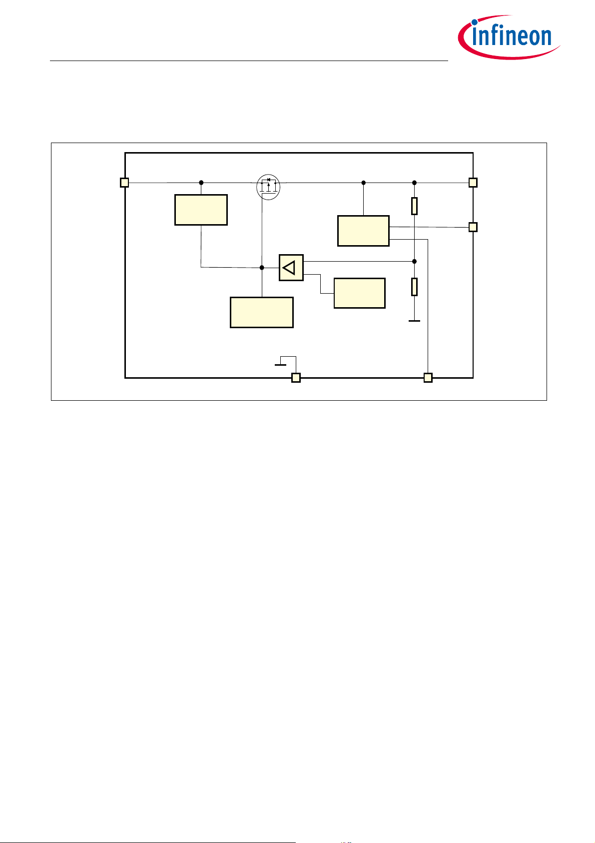
Bandgap
Reference
GND
Q
I
Temperature
Shutdown
Reset
RO
D
Current
Limitation
OPTIREG™ Linear TLS850C2TEVxx Demoboard
Introduction
1.3 Block Diagram
Figure 1 shows the block diagram of TLS850C2TEVxx.
Figure 1 Block Diagram of TLS850C2TEVxx.
User manual 5 Rev. 1.01
2020-10-21
Page 6

OPTIREG™ Linear TLS850C2TEVxx Demoboard
Demoboard
2 Demoboard
Figure 2 shows a TLS850C2TEVxx Demoboard equipped with TLS805D3MCV33.
Figure 2 TLS850C2TEVxx Demoboard
User manual 6 Rev. 1.01
2020-10-21
Page 7

OPTIREG™ Linear TLS850C2TEVxx Demoboard
Demoboard
2.1 Operating Conditions
To avoid any electrical damage of the Demoboard, the maximum operating range defined in Table 2 must be
followed.
Table 2 Operating Range
1)
Parameter Symbol Limit Values Unit Note
Min. Max.
2)
Board Supply Voltage
VIN 0 40 V Power supply
Regulator Output VOUT 0 7 V Regulated output voltage
Reset output Signal RO 0 7 V Indicates whether reset occurred
Ground GND 0 0 V System GND
1) The Demoboard operates at ambient temperature of 25°C.
2) Functional input voltage range starts from 3.0 V to 40 V.
2.2 Board Configuration
The TLS850C2TEVxx Demoboard can be easily configured via jumpers on the board. The board provides the
following configuration options:
• Reset timing selection (JP_CD)
• Placeholder for additional SMD output capacitors (C4)
• Placeholder for additional Through-Hole output capacitors (C5)
2.2.1 Power-on reset timing selection
Power-on reset delay timing can be configured by JP_CD; connecting pin D with the available delay
capacitors:
Table 3 Header options for reset delay timing
JP_CD Function
set to 10nF Power-on reset delay time is configured to typically 2.5 ms
set to 100nF Power-on reset delay time is configured to typically 25 ms
1) Without a defined capacitor on pin D the reset function is disabled.
1)
User manual 7 Rev. 1.01
2020-10-21
Page 8

OPTIREG™ Linear TLS850C2TEVxx Demoboard
Demoboard
2.2.2 Signal Adaption
For easy signal adaption e.g. connecting probes for an oscilloscope, test points VIN, VOUT, RO and GND can be
used.
Table 4 Signals on test point
Test point Accessible Signal
VIN Input voltage
VOUT Output voltage
RO Reset output signal
GND GND
User manual 8 Rev. 1.01
2020-10-21
Page 9

OPTIREG™ Linear TLS850C2TEVxx Demoboard
Schematic and Layout TLS850C2TEVxx Demoboard
3 Schematic and Layout TLS850C2TEVxx Demoboard
3.1 Schematic TLS850C2TEVxx Demoboard
Figure 3 Schematic of TLS850C2TEVxx Demoboard
User manual 9 Rev. 1.01
2020-10-21
Page 10

OPTIREG™ Linear TLS850C2TEVxx Demoboard
Schematic and Layout TLS850C2TEVxx Demoboard
3.2 Layout TLS850C2TEVxx Demoboard
Figure 4 Top Layer of TLS850C2TEVxx Demoboard
Figure 5 Bottom Layer of TLS850C2TEVxx Demoboard
User manual 10 Rev. 1.01
2020-10-21
Page 11

OPTIREG™ Linear TLS850C2TEVxx Demoboard
Bill of Material
4 Bill of Material
Table 5 Bill of Material
Part Value Package
IC1 TLS850C2TEV50 /
TLS850C2TEV33
VIN Banana jack BABU4MM
VOUT Banana jack BABU4MM
RO Banana jack BABU4MM
GND Banana jack BABU4MM
D1 Diode SE20F SMF (DO-219AB)
SJ1 Solder jumper
C1 47µF/50V E2,5-7
C2 10µF/16V C0805
C3 100nF/50V C0805
C4 n.a. C1206
C5 n.a. E2,5-7
JP_CD 3 pin connector
CD1 10nF/50V C0805
CD2 100nF/50V C0805
GND GND connector
PG-TO252-5
User manual 11 Rev. 1.01
2020-10-21
Page 12

OPTIREG™ Linear TLS850C2TEVxx Demoboard
General Information
5 General Information
5.1 Restrictions
This Demoboard is offering limited features allowing you only to evaluate and test the Infineon products. The
Demoboard is not an end product (or finished appliance), nor is it intended or authorized by Infineon to be
integrated into end products. The Demoboard may not be used in any production system.
5.2 Additional Information
For further information you may contact http://www.infineon.com/
User manual 12 Rev. 1.01
2020-10-21
Page 13

OPTIREG™ Linear TLS850C2TEVxx Demoboard
Revision History
6 Revision History
Revision Date Changes
1.01 2020-10-21 Editorial changes
1.0 2019-09-05 Initial version
User manual 13 Rev. 1.01
2020-10-21
Page 14

Trademarks of Infineon Technologies AG
All referenced product or service names and trademarks are the property of their respective owners.
IMPORTANT NOTICE
Edition 2020-10-21
Published by
Infineon Technologies AG
81726 Munich, Germany
© 2021 Infineon Technologies AG.
All Rights Reserved.
Do you have a question about any
aspect of this document?
Email: erratum@infineon.com
Document reference
Z8F66743815
The information contained in this application note is
given as a hint for the implementation of the product
only and shall in no event be regarded as a description
or warranty of a certain functionality, condition or
quality of the product. Before implementation of the
product, the recipient of this application note must
verify any function and other technical information
given herein in the real application. Infineon
Technologies hereby disclaims any and all warranties
and liabilities of any kind (including without limitation
warranties of non-infringement of intellectual
property rights of any third party) with respect to any
and all information given in this application note.
The data contained in this document is exclusively
intended for technically trained staff. It is the
responsibility of customer’s technical departments to
evaluate the suitability of the product for the intended
application and the completeness of the product
information given in this document with respect to
such application.
For further information on technology, delivery terms
and conditions and prices, please contact the nearest
Infineon Technologies Office (www.infineon.com).
WARNINGS
Due to technical requirements products may contain
dangerous substances. For information on the types
in question please contact your nearest Infineon
Technologies office.
Except as otherwise explicitly approved by Infineon
Technologies in a written document signed by
authorized representatives of Infineon Technologies,
Infineon Technologies’ products may not be used in
any applications where a failure of the product or any
consequences of the use thereof can reasonably be
expected to result in personal injury.
 Loading...