

Page 1

OPTIREG™ linear voltage regulator TLS115x0xx
demoboard
Z8F56253795
Preface
Scope and purpose
This document provides information about the usage of the demoboards for the voltage tracking regulators
TLS115x0EJ (PG-DSO-8 package variant) and the TLS115x0LD (PG-TSON-10 package variant) from Infineon
Technologies AG. Please also refer to the corresponding datasheets.
Intended audience
This document is intended for engineers who develop applications.
User manual Please read the Important Notice and Warnings at the end of this document Rev. 1.01
www.infineon.com/OPTIREG-linear 2021-02-11
Page 2

OPTIREG
™
linear voltage regulator TLS115x0xx demoboard
Z8F56253795
Table of contents
Table of contents
Preface . . . . . . . . . . . . . . . . . . . . . . . . . . . . . . . . . . . . . . . . . . . . . . . . . . . . . . . . . . . . . . . . . . . . . . . . . . . . . . . . .1
Table of contents . . . . . . . . . . . . . . . . . . . . . . . . . . . . . . . . . . . . . . . . . . . . . . . . . . . . . . . . . . . . . . . . . . . . . . . 2
1 Introduction . . . . . . . . . . . . . . . . . . . . . . . . . . . . . . . . . . . . . . . . . . . . . . . . . . . . . . . . . . . . . . . . . . . . . . . . . . . 3
1.1 TLS115x0xx family and features . . . . . . . . . . . . . . . . . . . . . . . . . . . . . . . . . . . . . . . . . . . . . . . . . . . . . . . . . . . 3
1.2 Block diagram . . . . . . . . . . . . . . . . . . . . . . . . . . . . . . . . . . . . . . . . . . . . . . . . . . . . . . . . . . . . . . . . . . . . . . . . . . .4
2 Demoboard . . . . . . . . . . . . . . . . . . . . . . . . . . . . . . . . . . . . . . . . . . . . . . . . . . . . . . . . . . . . . . . . . . . . . . . . . . . . 5
2.1 Operating conditions . . . . . . . . . . . . . . . . . . . . . . . . . . . . . . . . . . . . . . . . . . . . . . . . . . . . . . . . . . . . . . . . . . . . 6
2.2 Demoboard configuration . . . . . . . . . . . . . . . . . . . . . . . . . . . . . . . . . . . . . . . . . . . . . . . . . . . . . . . . . . . . . . . . 6
2.2.1 Jumpers . . . . . . . . . . . . . . . . . . . . . . . . . . . . . . . . . . . . . . . . . . . . . . . . . . . . . . . . . . . . . . . . . . . . . . . . . . . . . . 6
2.2.2 Signal adaption . . . . . . . . . . . . . . . . . . . . . . . . . . . . . . . . . . . . . . . . . . . . . . . . . . . . . . . . . . . . . . . . . . . . . . . .8
3 Schematic and layout . . . . . . . . . . . . . . . . . . . . . . . . . . . . . . . . . . . . . . . . . . . . . . . . . . . . . . . . . . . . . . . . . . .9
3.1 Schematic . . . . . . . . . . . . . . . . . . . . . . . . . . . . . . . . . . . . . . . . . . . . . . . . . . . . . . . . . . . . . . . . . . . . . . . . . . . . . . 9
3.2 Layout . . . . . . . . . . . . . . . . . . . . . . . . . . . . . . . . . . . . . . . . . . . . . . . . . . . . . . . . . . . . . . . . . . . . . . . . . . . . . . . . 10
4 Bill of materials . . . . . . . . . . . . . . . . . . . . . . . . . . . . . . . . . . . . . . . . . . . . . . . . . . . . . . . . . . . . . . . . . . . . . . . 14
5 Restrictions . . . . . . . . . . . . . . . . . . . . . . . . . . . . . . . . . . . . . . . . . . . . . . . . . . . . . . . . . . . . . . . . . . . . . . . . . . . 15
6 Revision history . . . . . . . . . . . . . . . . . . . . . . . . . . . . . . . . . . . . . . . . . . . . . . . . . . . . . . . . . . . . . . . . . . . . . . . 16
Disclaimer . . . . . . . . . . . . . . . . . . . . . . . . . . . . . . . . . . . . . . . . . . . . . . . . . . . . . . . . . . . . . . . . . . . . . . . . . . . . 17
User manual 2 Rev. 1.01
2021-02-11
Page 3
OPTIREG™ linear voltage regulator TLS115x0xx demoboard
Z8F56253795
Introduction
1 Introduction
1.1 TLS115x0xx family and features
TLS115x0xx family
Table 1 TLS115x0xx family
Type Package Output current Enable Power good Adjustable
TLS115B0EJ PG-DSO-8 150 mA ✓ – ✓
TLS115D0EJ PG-DSO-8 150 mA ✓ ✓ ✓
TLS115B0LD PG-TSON-10 150 mA ✓ – ✓
TLS115D0LD PG-TSON-10 150 mA ✓ ✓ ✓
TLS115x0xx features
• 150 mA current capability
• Very high accuracy voltage tracking
• Output voltage adjustable down to 2.0 V
• Very low dropout voltage
• Very low current consumption in OFF mode
• Power good output indicates overvoltage and undervoltage
• Internally controlled so start
• Green Product (RoHS compliant)
• AEC qualified
Additional benefits of the TLS115x0xx voltage tracking regulators:
• Fast regulation
• Very good stability characteristics
• Only a small ceramic capacitor of 1 μF at the output is required
• Internal protection features make the devices robust against immediate damage:
- Output current limitation
- Short circuit protected output (to GND and to battery)
- Overtemperature shutdown
- Reverse polarity protected input
These features make the TLS115x0xx voltage tracking regulators perfectly suitable as automotive sensor supply
and as high precision supply for o-board loads.
1)
1
Valid for TLS115D0.
User manual 3 Rev. 1.01
2021-02-11
Page 4
OPTIREG
Z8F56253795
Introduction
™
linear voltage regulator TLS115x0xx demoboard
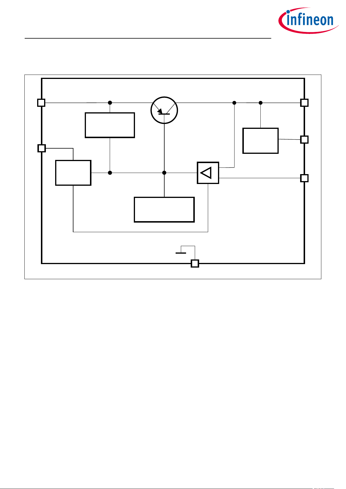
1.2 Block diagram
IN
EN
Enable
Protection
Circuits
Temperature
Shutdown
GND
Power
Good
OUT
PG
ADJ
Figure 1 Block diagram
User manual 4 Rev. 1.01
2021-02-11
Page 5
OPTIREG
™
linear voltage regulator TLS115x0xx demoboard
Z8F56253795
Demoboard
2 Demoboard
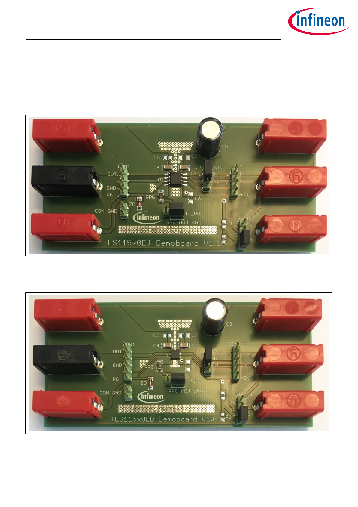
The OPTIREG™ linear voltage regulator TLS115x0xx demoboard is available for all devices of the TLS115x0xx
voltage tracking regulator family in a PG-DSO-8 or PG-TSON-10 package, see the device list in Table 1.
Figure 2 shows the OPTIREG™ linear voltage regulator TLS115x0EJ demoboard equipped with TLS115D0EJ
(PG-DSO-8 package).
Figure 2 OPTIREG™ linear voltage regulator TLS115x0EJ demoboard
Figure 3 shows the OPTIREG™ linear voltage regulator TLS115x0LD demoboard equipped with TLS115D0LD
(PG-TSON-10 package).
Figure 3 OPTIREG™ linear voltage regulator TLS115x0LD demoboard
User manual 5 Rev. 1.01
2021-02-11
Page 6

OPTIREG™ linear voltage regulator TLS115x0xx demoboard
Z8F56253795
Demoboard
2.1 Operating conditions
To avoid electrical damage of the demoboard, the operating range defined in Table 2 must be maintained.
Table 2 Limit values for operation
2)
Parameter Pin Maximum Ratings Unit Note
Min. Max.
Board supply voltage
Adjust voltage
4)
3)
VIN -16 45 V Power supply
VADJ -16 45 V Tracked reference voltage
Regulator output voltage VOUT -5 45 V –
Enable input signal EN -16 45 V Enables or disables the voltage tracking
regulator
Power good output signal PG -0.3 7 V Indicates, whether Power good
conditions are met
Ground GND 0 0 V System GND
2.2 Demoboard configuration
The jumper pins and solder pads on the demoboard provide easy to use configuration options.
Jumper connections
• EN input pin ↔ supply voltage pin VIN (JP_EN_VIN)
• ADJ pin ↔ EN pin or
ADJ pin ↔ external voltage divider
to adjust the reference voltage depending on voltage at VIN pin (JP_ADJ)
• ADJ pin ↔ RPG pin
as pull-up voltage for the power good resistor RPG (JP_PG)
Solder pads for components
• Additional input capacitor C2
• additional output capacitor C5
• Adjust capacitor C6
• Voltage divider resistor R1
• Voltage divider resistor R2
2.2.1 Jumpers
The unlabeled pin of each jumper can take an unused connector to leave the connection open.
Jumper JP_EN_VIN
The JP_EN_VIN jumper can connect the EN input pin to the supply voltage at the VIN pin.
2
The demoboard operates at an ambient temperature of 25°C.
3
Functional input voltage range: 4 V to 45 V.
4
Functional ADJ voltage range: 2 V to 14 V.
User manual 6 Rev. 1.01
2021-02-11
Page 7

OPTIREG™ linear voltage regulator TLS115x0xx demoboard
Z8F56253795
Demoboard
Table 3 Jumper JP_EN_VIN options for Enable function
JP_EN_VIN Function
EN input pin ↔ VIN pin The regulator is enabled while it is supplied from the voltage at the VIN pin
open The EN input pin is supplied from the EN banana jack connector
Jumper JP_ADJ
The JP_ADJ jumper can connect the ADJ pin of the device to one of the following:
• The voltage at the EN pin (VEN), if the ADJ pin is not supplied from an external voltage
• A reference voltage (VD) adapted by the voltage divider on the demoboard
Table 4 Jumper JP_ADJ options for reference voltage
JP_ADJ Function
ADJ pin ↔ EN input pin The ADJ pin is connected to the voltage at the EN pin
5)
ADJ pin ↔ V
D
open The ADJ pin must be supplied from external via ADJ banana jack connector.
The ADJ pin is connected to the output voltage of the voltage divider (VD)
6)
If the ADJ pin is to be supplied from the output voltage of the voltage divider (VD), then the resistors of the
voltage divider must be implemented. The value of the resistors can be easily calculated when neglecting the
current flowing into the ADJ pin:
R
V
ADJ
= VD=
2
R1+ R
2
× V
IN
Equation 1
The current flowing into the ADJ pin can be neglected, if R2 is less than 2.5 kΩ. To benefit from the high accuracy
of the TLS115x0, it is highly recommended to supply the ADJ pin from an external voltage source via the banana
jack connector.
PG Jumper
With jumper JP_PG, the voltage at the ADJ pin can be used as pull-up voltage for the power good resistor RPG.
The power good signal, which then corresponds to the voltage at the ADJ pin, can then be measured at the
PG connector of the demoboard. To protect the the device from overvoltage, the PG connector is clamped by a
Z-diode to typically 6.2 V.
Table 5 Jumper JP_PG options for power good function
JP_PG Function
PG ↔ ADJ pin The voltage applied at the ADJ pin is used as pull-up voltage for the power good
resistor RPG. Power good monitoring is enabled.
open No pull-up voltage is applied to the power good resistor RPG. Power good
monitoring is disabled.
5
Without supplying a signal to EN, the regulator is disabled because of the internal pull-down resistor.
6
Without supplying a reference voltage to ADJ, the regulator is disabled.
User manual 7 Rev. 1.01
2021-02-11
Page 8

OPTIREG™ linear voltage regulator TLS115x0xx demoboard
Z8F56253795
Demoboard
2.2.2 Signal adaption
The connectors CON1, CON2 and CON_GND oer easy signal adaption, for example with probes for an
oscilloscope.
Table 6 Signals on connector
Connector Accessible signal
CON1 • OUT (output voltage)
• GND (ground)
• PG (power good signal)
CON2 • IN (input voltage)
• EN (Enable input signal)
• ADJ (reference voltage)
CON_GND • GND (ground)
User manual 8 Rev. 1.01
2021-02-11
Page 9

OPTIREG
™
linear voltage regulator TLS115x0xx demoboard
Z8F56253795
Schematic and layout
3 Schematic and layout
3.1 Schematic
Figure 4 Schematic OPTIREG™ linear voltage regulator TLS115x0EJ demoboard
Figure 5 Schematic OPTIREG™ linear voltage regulator TLS115x0LD demoboard
User manual 9 Rev. 1.01
2021-02-11
Page 10

OPTIREG
™
linear voltage regulator TLS115x0xx demoboard
Z8F56253795
Schematic and layout
3.2 Layout
Figure 6 Top layer OPTIREG™ linear voltage regulator TLS115x0EJ demoboard
User manual 10 Rev. 1.01
2021-02-11
Page 11

OPTIREG
™
linear voltage regulator TLS115x0xx demoboard
Z8F56253795
Schematic and layout
Figure 7 Bottom layer OPTIREG™ linear voltage regulator TLS115x0EJ demoboard
User manual 11 Rev. 1.01
2021-02-11
Page 12

OPTIREG
™
linear voltage regulator TLS115x0xx demoboard
Z8F56253795
Schematic and layout
Figure 8 Top layer OPTIREG™ linear voltage regulator TLS115x0LD demoboard
User manual 12 Rev. 1.01
2021-02-11
Page 13

OPTIREG
™
linear voltage regulator TLS115x0xx demoboard
Z8F56253795
Schematic and layout
Figure 9 Bottom layer OPTIREG™ linear voltage regulator TLS115x0LD demoboard
User manual 13 Rev. 1.01
2021-02-11
Page 14

OPTIREG™ linear voltage regulator TLS115x0xx demoboard
Z8F56253795
Bill of materials
4 Bill of materials
Table 7 Bill of materials
Part Value Package
U1 One of the following:
• TLS115B0EJ or TLS115D0EJ
• TLS115B0LD or TLS115D0LD
VIN Banana jack BABU4MM
VOUT Banana jack BABU4MM
EN Banana jack BABU4MM
PG Banana jack BABU4MM
GND Banana jack BABU4MM
R1 n.a. R0805
R2 n.a. R0805
RPG 10 kΩ R1206
C1 100 nF / 50 V C1206
C2 n.a. C1206
C3 10 µF / 50 V E5-8.5
C4 1 µF / 16 V C1206
C5 n.a. C0805
One of the following:
• PG-DSO-8
• PG-TSON-10
C6 n.a. C1206
CON1 4 pin connector –
CON2 4 pin connector –
CON_GND 2 pin connector –
JP_EN_VIN – Jumper
JP_ADJ – Jumper
JP_PG – Jumper
ZD Z-diode ZMM6.2 (6.2 V) SOD80C
User manual 14 Rev. 1.01
2021-02-11
Page 15

OPTIREG™ linear voltage regulator TLS115x0xx demoboard
Z8F56253795
Restrictions
5 Restrictions
This demoboard oers limited features only for evaluation and testing of Infineon products. The demoboard is
not an end product or finished appliance, nor is it intended or authorized by Infineon to be integrated into end
products. The demoboard may not be used in any production system.
For further information please visit www.infineon.com.
User manual 15 Rev. 1.01
2021-02-11
Page 16

OPTIREG™ linear voltage regulator TLS115x0xx demoboard
Z8F56253795
Revision history
6 Revision history
Revision Date Changes
1.01 2021-02-11 Editorial changes
1.0 2016-02-22 Document created
User manual 16 Rev. 1.01
2021-02-11
Page 17

Trademarks
All referenced product or service names and trademarks are the property of their respective owners.
Edition 2021-02-11
Published by
Infineon Technologies AG
81726 Munich, Germany
©
2021 Infineon Technologies AG
All Rights Reserved.
Do you have a question about any
aspect of this document?
Email: erratum@infineon.com
Document reference
IFX-Z8F56253795
IMPORTANT NOTICE
The information given in this document shall in no
event be regarded as a guarantee of conditions or
characteristics (“Beschaenheitsgarantie”).
With respect to any examples, hints or any typical
values stated herein and/or any information regarding
the application of the product, Infineon Technologies
hereby disclaims any and all warranties and liabilities
of any kind, including without limitation warranties of
non-infringement of intellectual property rights of any
third party.
In addition, any information given in this document is
subject to customer’s compliance with its obligations
stated in this document and any applicable legal
requirements, norms and standards concerning
customer’s products and any use of the product of
Infineon Technologies in customer’s applications.
The data contained in this document is exclusively
intended for technically trained sta. It is the
responsibility of customer’s technical departments to
evaluate the suitability of the product for the intended
application and the completeness of the product
information given in this document with respect to such
application.
WARNINGS
Due to technical requirements products may contain
dangerous substances. For information on the types
in question please contact your nearest Infineon
Technologies oice.
Except as otherwise explicitly approved by Infineon
Technologies in a written document signed by
authorized representatives of Infineon Technologies,
Infineon Technologies’ products may not be used in
any applications where a failure of the product or
any consequences of the use thereof can reasonably
be expected to result in personal injury.
 Loading...