

Page 1

User Manual 1 Ver. 1.11
www.infineon.com/sensors 2019-05-28
TLI493D-A2B6
Low Power 3D Hall Sensor with I2 C Interface
User Manual
About this document
Scope and purpose
This document provides product information and descriptions regarding:
2
•I
C Registers
2
•I
C Interface
• Diagnostic
Intended audience
This document is aimed at engineers and developers of hard and software using the sensor TLI493D-A2B6.
Page 2

TLI493D-A2B6
Table of contents
Table of contents
1I
2
C Registers . . . . . . . . . . . . . . . . . . . . . . . . . . . . . . . . . . . . . . . . . . . . . . . . . . . . . . . . . . . . . . . . . . . . . . . . . . . . . . 3
1.1 Registers overview . . . . . . . . . . . . . . . . . . . . . . . . . . . . . . . . . . . . . . . . . . . . . . . . . . . . . . . . . . . . . . . . . . . . . . . . 3
1.2 Register descriptions . . . . . . . . . . . . . . . . . . . . . . . . . . . . . . . . . . . . . . . . . . . . . . . . . . . . . . . . . . . . . . . . . . . . . . 4
1.2.1 Bit types . . . . . . . . . . . . . . . . . . . . . . . . . . . . . . . . . . . . . . . . . . . . . . . . . . . . . . . . . . . . . . . . . . . . . . . . . . . . . . . 4
1.2.2 Measurement data and registers combined in the I
2
1.2.3 Configuration registers combined in the I
1.2.4 Mode registers combined in the I
2
C parity flag “FF” . . . . . . . . . . . . . . . . . . . . . . . . . . . . . . . . . . . . . . . . . 8
C parity flag “CF” . . . . . . . . . . . . . . . . . . . . . . . . . . . . . . . . . 7
2
C parity bit “P” . . . . . . . . . . . . . . . . . . . . . . . . . . 4
1.2.5 Diagnostic, status and version registers . . . . . . . . . . . . . . . . . . . . . . . . . . . . . . . . . . . . . . . . . . . . . . . . . . 10
2I
2.1 I
2
C Interface . . . . . . . . . . . . . . . . . . . . . . . . . . . . . . . . . . . . . . . . . . . . . . . . . . . . . . . . . . . . . . . . . . . . . . . . . . . . . 13
2
C protocol description . . . . . . . . . . . . . . . . . . . . . . . . . . . . . . . . . . . . . . . . . . . . . . . . . . . . . . . . . . . . . . . . . . 13
2.1.1 General description . . . . . . . . . . . . . . . . . . . . . . . . . . . . . . . . . . . . . . . . . . . . . . . . . . . . . . . . . . . . . . . . . . . . 13
2.1.2 I2C write command . . . . . . . . . . . . . . . . . . . . . . . . . . . . . . . . . . . . . . . . . . . . . . . . . . . . . . . . . . . . . . . . . . . . . 13
2.1.3 I2C read commands . . . . . . . . . . . . . . . . . . . . . . . . . . . . . . . . . . . . . . . . . . . . . . . . . . . . . . . . . . . . . . . . . . . . 17
2.1.3.1 2-byte read command . . . . . . . . . . . . . . . . . . . . . . . . . . . . . . . . . . . . . . . . . . . . . . . . . . . . . . . . . . . . . . . . 17
2.1.3.2 1-byte read command . . . . . . . . . . . . . . . . . . . . . . . . . . . . . . . . . . . . . . . . . . . . . . . . . . . . . . . . . . . . . . . . 17
2.2 Collision avoidance and clock stretching . . . . . . . . . . . . . . . . . . . . . . . . . . . . . . . . . . . . . . . . . . . . . . . . . . . 19
2.2.1 Collision avoidance (CA bit = 0
2.2.2 Clock stretching (CA bit = 0
2.3 Sensor reset by I
2
C . . . . . . . . . . . . . . . . . . . . . . . . . . . . . . . . . . . . . . . . . . . . . . . . . . . . . . . . . . . . . . . . . . . . . . . 21
and INT bit = 0B) . . . . . . . . . . . . . . . . . . . . . . . . . . . . . . . . . . . . . . . . . . 19
B
and INT bit = 1B) . . . . . . . . . . . . . . . . . . . . . . . . . . . . . . . . . . . . . . . . . . . . . 20
B
2.4 Sensor Initialization and Readout example . . . . . . . . . . . . . . . . . . . . . . . . . . . . . . . . . . . . . . . . . . . . . . . . . 22
2.5 Loss of V
impact on I2C bus . . . . . . . . . . . . . . . . . . . . . . . . . . . . . . . . . . . . . . . . . . . . . . . . . . . . . . . . . . . . . 23
DD
3 Diagnostic . . . . . . . . . . . . . . . . . . . . . . . . . . . . . . . . . . . . . . . . . . . . . . . . . . . . . . . . . . . . . . . . . . . . . . . . . . . . . . 24
3.1 Parity bits and parity flags . . . . . . . . . . . . . . . . . . . . . . . . . . . . . . . . . . . . . . . . . . . . . . . . . . . . . . . . . . . . . . . . 24
3.2 Power-down flags . . . . . . . . . . . . . . . . . . . . . . . . . . . . . . . . . . . . . . . . . . . . . . . . . . . . . . . . . . . . . . . . . . . . . . . 24
3.3 Frame Counter . . . . . . . . . . . . . . . . . . . . . . . . . . . . . . . . . . . . . . . . . . . . . . . . . . . . . . . . . . . . . . . . . . . . . . . . . . 24
4 Terminology . . . . . . . . . . . . . . . . . . . . . . . . . . . . . . . . . . . . . . . . . . . . . . . . . . . . . . . . . . . . . . . . . . . . . . . . . . . . 25
5 Revision history . . . . . . . . . . . . . . . . . . . . . . . . . . . . . . . . . . . . . . . . . . . . . . . . . . . . . . . . . . . . . . . . . . . . . . . . . 26
User Manual 2 Ver. 1.11
2019-05-28
Page 3
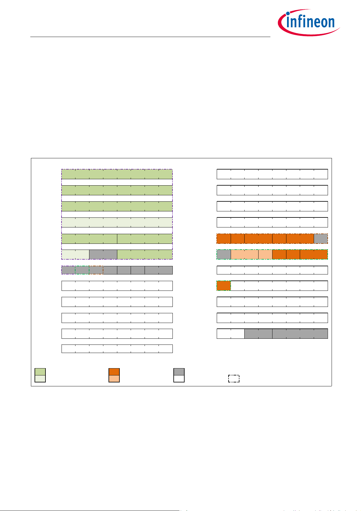
76543210 76543210
Bx (00
)0C
By (01H)0D
Bz (02H)0E
Temp (03H)0F
Bx2 (04H)Config (10
)DTAM X2 CP
w
Temp2 (05H)MOD1 (11
)FP PR CAINT
rw rw rw rw rw rw
rrrrrr
07
MOD 2 (13H)PRD
rw
08
14
09
15
0A
Ver (16H)
Reserved
Reserved
Reserved
Reserved
Reserved
Reserved
TL_mag
Reserved
Reserved Type HWV
Bz (11…4)
Temp (11…4)
r
Bx (3…0) By (3…0)
Bx (11…4)
Reserved
TRIG
r
By (11…4)
Temp (3…2) ID
Reserved
Bz (3…0)
r
Reserved
Reserved
MOD E
r
IICadr
rrw
Colour legend for the Bitmap
Magnetic values Configuration Diagnosis
Temperature values Confi guration bus Res erved bits Parity bits and related registers (colour)
TLI493D-A2B6
I2C Registers
1I
2
C Registers
The TLI493D-A2B6 includes several registers that can be accessed via Inter-Integrated Circuit interface (I2C) to
read data as well as to write and configure settings.
1.1 Registers overview
A bitmap overview is presented in Figure 1. Basically the following sections are available:
• measurement data (green bits in registers 00
• sensor status and diagnostics (grey bits in registers 05
• configuration parameters such as the power mode (orange bits in registers 10
H
r
r
r
till 05H)
H
, 06H, 10H and 11H)
H
H
H
H
H
, 11H and 13H)
H
H
rr
Diag (06H)P FFCF TPD3PD0 12
H
H
Figure 1 TLI493D-A2B6 Bitmap
The diagnostic register 06
and marks the relationship of the sections to this flags with different colored lines/frames around the bit
H
H
0B
H
H
Reserved
contains parity information as a diagnostic mechanism. The bitmap illustrates this
FRM
rw r
H
H
H
H
rw
rr
rw rw
Reserved
rw
contents.
User Manual 3 Ver. 1.11
2019-05-28
Page 4
TLI493D-A2B6
I2C Registers
Table 1 Registers overview
Register name Register long name Address
Bx, By and Bz Magnetic values MSBs 00
Temp Temperature value MSBs 03
Bx2 Magnetic values LSBs 04
Temp2 Temperature and magnetic LSBs and device address 05
Diag Sensor diagnostic and status register 06
Config Configuration register 10
MOD1 Power mode, interrupt, address, parity 11
MOD2 Low Power Mode update rate 13
Ver Version register 16
, 01H, 02
H
H
H
H
H
H
H
H
H
H
1.2 Register descriptions
The I2C registers can be read or written at any time. It is recommended to read measurement data in a
synchronized fashion, i.e. after an interrupt pulse (/INT). This avoids reading inconsistent sensor or diagnostic
data, especially in fast mode. Additionally, several flags can be checked to ensure the register values are
consistent and the ADC was not running at the time of readout.
1.2.1 Bit types
The TLI493D-A2B6 contains read bits, write bits and reserved bits.
Table 2 Bit Types
Abbreviation Function Description
r Read Read-only bits
rw Read Write Readable and writable bit
Reserved Bits that must keep the default values (read prior to write required)
1.2.2 Measurement data and registers combined in the I2C parity bit “P”
The I2C communication of the registers in this chapter is protected with the parity bit “P”, described in the Diag
register with the address 06
To make sure all data is consistent, the registers from 00
Otherwise, the sampled data (X, Y, Z, Temperature) may correspond to different conversion cycles.
. See also Figure 1 - parity bits and related registers.
H
to 06H should be read with the same I2C command.
H
User Manual 4 Ver. 1.11
2019-05-28
Page 5

7 0
Bx, By and Bz (11...4)
7 0
Temp (11...4)
7 0
Bx (3...0)
By (3...0)
43
TLI493D-A2B6
I2C Registers
Magnetic values MSBs
Register names Address Reset Value
Bx, By and Bz 00
01H 02
H
Field Bits Type Description
Bx, By and Bz 7:0 r Bx, By and Bz values
Signed value as two’s complement from the HALL probes in the x, y and zdirection of the magnetic field. Contains the eight Most Significant Bits.
If Bz is deactivated the Bz value is the reset value.
H
80
H
Back to TLI493D-A2B6 Bitmap.
Temperature value MSBs
Register name Address Reset Value
Temp 03
H
80
Field Bits Type Description
Temp 7:0 r Temperature value
Signed value as two’s complement.
If the temperature measurement is deactivated, the Temp value is the
reset value.
Back to TLI493D-A2B6 Bitmap.
H
Magnetic values LSBs
Register name Address Reset Value
Bx2 04
User Manual 5 Ver. 1.11
H
00
2019-05-28
H
Page 6

7 0
Bz (3...0)
43
Temp (3...2)
ID
65
TLI493D-A2B6
I2C Registers
Field Bits Type Description
Bx 7:4 r Bx value
Signed value as two’s complement from the HALL probes in the xdirection of the magnetic field.
Contains the four Least Significant Bits.
By 3:0 r By value
Signed value as two’s complement from the HALL probes in the ydirection of the magnetic field.
Contains the four Least Significant Bits.
Back to TLI493D-A2B6 Bitmap.
Temperature and magnetic LSBs and device address
Register name Address Reset Value
Temp2 05
H
00
Field Bits Type Description
Temp 7:6 r Temperature value
Signed value as two’s complement.
If the temperature measurement is deactivated, the Temp value is the
reset value.
ID 5:4 r ID
Readback of the sensor ID, from IICadr. µC shall verify the address sent by
the sensor. See Table 4.
Bz 3:0 r Bz value
Signed value as two’s complement from the HALL probes in the zdirection of the magnetic field.
Contains the four Least Significant Bits.
If Bz is deactivated the Bz value is 0
.
H
H
Back to TLI493D-A2B6 Bitmap.
User Manual 6 Ver. 1.11
2019-05-28
Page 7

7 0
CP
6
5
4
3
21
TL_magX2AMDT TRIG
TLI493D-A2B6
I2C Registers
1.2.3 Configuration registers combined in the I2C parity flag “CF”
The I2C communication of the registers in this chapter is protected by the parity bit CF, which is described in
the Diag register with the address 06
Configuration register
Register name Address Reset Value
Config 10
. See also Figure 1 - parity bits and related registers.
H
H
00
H
Field Bits Type Description
DT 7rwDisable Temperature
temperature measurement is enabled.
If 0
B
If 1
temperature measurement is disabled. This means the Bx, By and Bz
B
channels are measured. The Temp channel is disabled and contains the
reset value until a new conversion with Temp is done.
AM 6rwX/Y Angular Measurement
the Bz measurement is enabled.
If 0
B
If 1
and the DT bit = 1B the Bz measurement is disabled. This means the
B
Bx and By channel is measured. The channels Bz and Temp contain the
reset values until a new conversion with Bz and Temp is done.
Note: If the DT bit = 0
, the AM bit don’t care.
B
TRIG 5:4 rw Trigger options
If PR bit = 1
(1-byte read protocol), the TRIG bits define the trigger mode
B
of the device:
If 00
no ADC trigger on read.
B
If 01
ADC trigger on read before first MSB.
B
ADC trigger on read after register 05H.
If 1x
B
If PR bit = 0
these bits have no effect.
B
X2 3rwShort-range sensitivity
When this bit is set, the sensitivity of the Bx, By, and Bz ADC-conversion is
doubled by a longer ADC integration time. The Temp result will not
change, neither in sensitivity nor conversion time. See Table 3.
TL_mag 2:1 rw Magnetic temperature compensation
There are two bits for setting the sensitivity over temperature of the
sensor to compensate a magnet temperature coefficient.
If 00
→ TC0 (no compensation)
B
→ TC1
If 01
B
If 10
→ TC2
B
If 11
→ TC3
B
CP 0rwConfiguration parity
The register 10
this parity is OK and the CF bit in the status register 06
User Manual 7 Ver. 1.11
is even parity protected with this bit. On startup or reset,
H
is set.
H
2019-05-28
Page 8

7 0
FP
6 321
PR INT MODE
54
IICadr CA
TLI493D-A2B6
I2C Registers
Back to TLI493D-A2B6 Bitmap.
Table 3 X2 bit
X2 bit Bx (11 ... 0) By (11 ... 0) Bz (11 ... 0) T (11 ... 2)
0
B
1
B
Bx full-range By full-range Bz full-range T full-range
Bx short-range By short-range Bz short-range T full-range
1.2.4 Mode registers combined in the I2C parity flag “FF”
The I2C communication of the registers in this chapter is protected with the parity bit “FF”, described in the
Diag register with the address 06
. See also Figure 1 - parity bits and related registers.
H
Power mode, interrupt, address, parity
Register name Address Reset Value
MOD1 11
H
00
Field Bits Type Description
H
FP 7rwFuse parity
The registers 11
and 13H (bit 7) are odd parity protected with this bit.
H
If this parity bit is incorrect please see FF bit.
To exit this state a sensor reset is necessary.
IICadr 6:5 rw I
2
C address
Bits can be set to 00
, 01B, 10B or 11B to define the slave address in bus
B
configuration.
See Table 4 and data sheet.
PR 4rwI2C 1-byte or 2-byte read protocol
this is the 2-byte read protocol:
If 0
B
<start> <I2Cadr.> <reg.adr.> <data of reg.adr.> <data of reg.adr.+1> ….
<stop>
If 1
this is the 1-byte read protocol:
B
<start> <I2Cadr.> <data of reg.00
See Chapter 2.1.3
CA 3rwCollision avoidance
Clock stretching only in master-controlled and low-power mode, not in
fast mode.
The CA bit interacts with the INT bit, see Table 5 and Chapter 2.2.
> <data of reg.01H> …. <stop>
H
User Manual 8 Ver. 1.11
2019-05-28
Page 9
TLI493D-A2B6
I2C Registers
Field Bits Type Description
INT 2rwInterrupt enabled
/INT disabled
If 1
B
If 0
/INT enabled: After a completed measurement and ADC-conversion,
B
an /INT pulse will be generated.
For bus configurations /INT timing constraints between I
and interrupt pulses must be monitored and aligned.
The INT bit interacts with the CA bit, see Table 5.
MODE 1:0 rw Power mode
Low Power Mode:
If 00
B
Cyclic measurements and ADC-conversions with a update rate, defined in
the PRD registers. “No ADC trigger” must be used, see Table 6 and TRIG.
If 01
Master Controlled Mode (Power Down mode):
B
Measurement triggering depends on the PR bit and is possible with I
sub address byte (see Table 6) or TRIG bits.
If 10
is reserved and must not be used.
B
If 11
Fast Mode:
B
The measurements and ADC-conversions are running continuously. It is
recommended to set INT = 0
2
C data transfers
and use a I2C clock speed ≥ 800 kHz.
B
2
C
Back to TLI493D-A2B6 Bitmap.
Table 4 Device address overview
The addresses are selected to ensure a minimum Hamming distance of 4 between them.
Address write Address read IICadr (bit-6) IICadr (bit-5) ID (bit-5) ID (bit-4)
1)
6A
H
44
H
F0
H
88
H
1) Default address after start up or reset.
6B
45
F1
89
1)
H
H
H
H
0
B
0
B
1
B
1
B
0
B
1
B
0
B
1
B
0
B
0
B
1
B
1
B
0
B
1
B
0
B
1
B
Table 5 /INT (interrupt) and clock stretching
In case the microcontroller tries to read sensor data the clock stretching pulls the SCL /INT line to low, as long
as the measurement and ADC-conversion is not finished.
CA INT Configuration
0
0
B
/INT is enabled and will not be transmitted between <START> and <STOP>.
B
/INT collision avoidance active.
1
0
B
/INT disabled. Clock stretching enabled.
B
Suppress sensor read out during ongoing ADC conversion.
This configuration must not be used with the “read” trigger-bits (7:5) = 010
or with the trigger option TRIG bit = 01
1
0
B
/INT is enabled and will be transmitted between <START> and <STOP>.
B
/INT may collide with I
2
C clock from microcontroller.
.
B
or 011B (see Table 6)
B
1
1
B
/INT disabled. Clock stretching disabled.
B
Unsynchronized sensor readouts may collide with ADC conversion.
User Manual 9 Ver. 1.11
2019-05-28
Page 10

7 0
PRD
Reserved
6
7 0
FRM
6
5
4
3
2
1
PD0PD3TCFFFP
TLI493D-A2B6
I2C Registers
Low Power Mode update rate
Register name Address Reset Value
MOD2 13
Field Bits Type Description
PRD 7rwUpdate rate settings
If 0
If 1
B fUpdate
B fUpdate
= fast.
= slow.
Reserved 6:0 Factory settings
H
(bits 7:5) 000
B
Back to TLI493D-A2B6 Bitmap.
1.2.5 Diagnostic, status and version registers
The device provides diagnostic and status information in register 06H and version information in register 16H.
Sensor diagnostic and status register
Register name Address Reset Value
Diag 06
Field Bits Type Description
P 7r Bus parity
This bit adds up to an odd parity of the registers 00
(including 05
), described in Chapter 1.2.2.
H
The parity bit is generated during the I
register byte and acknowledge bits are not included in the parity sum.
If the parity calculated by the microcontroller after I
these values must be treated as invalid.
H
through 05H
H
2
C readout. The address byte,
2
C reads is incorrect,
60
H
User Manual 10 Ver. 1.11
2019-05-28
Page 11

TLI493D-A2B6
I2C Registers
Field Bits Type Description
FF 6r Fuse parity flag
Provid es a flag from the internal fuse p arity check of registers 11
(bit 7). This parity check includes the FP bit.
If 1
parity is OK.
B
If 0
the parity is not correct. The sensor must be considered defective
B
and must no longer be used. A sensor with an invalid fuse parity
disconnects its SDA. It will automatically go to low-power mode and only
uses the /INT signal to communicate the error (collision avoidance is
enabled).
CF 5rConfiguration parity flag
Provides a flag from the internal configuration parity check of register
10
. This parity check includes the CP bit.
H
After startup or after reset the CP bit is true.
If 1
parity is OK.
B
parity is not OK.
If 0
B
T 4r T bit
data in registers 00H till 05H are invalid measurement data.
If 1
B
If 0
data in registers 00H till 05H are valid measurement data.
B
PD3 3rPower-down flag 3
If 1
ADC-conversion of Temp is completed and valid measurement data
B
can be read out. Thus it must be 1
ADC-conversion of Temp is running and read measurement data are
If 0
B
invalid. Any readout with PD3 bit = 0
At startup, this is 0
value then changes to 1
PD0 2rPower-down flag 0
the ADC conversion of Bx is completed and valid measurement data
If 1
B
can be read out. Thus it must be 1
If 0
the ADC conversion of Bx is running and read measurement data are
B
invalid. Any readout with PD0 bit = 0
At startup, this is 0
value then changes to 1
FRM 1:0 r Frame counter
Increments at every updated ADC-conversion, once a X/Y/Z/T or X/Y/Z or
X/Y conversion is completed and the new measurement data have been
stored in the registers 00
The microcontroller shall check if bits change in consecutive conversion
runs.
until one ADC conversion has been performed. The
B
until one ADC conversion has been performed. The
B
.
B
.
B
till 05H.
H
at readout.
B
should be considered invalid.
B
at readout.
B
should be considered invalid.
B
and 13H
H
Back to TLI493D-A2B6 Bitmap.
User Manual 11 Ver. 1.11
2019-05-28
Page 12

7 0
Reserved
HWV
43
TYPE
65
TLI493D-A2B6
I2C Registers
Version register
Register name Address Reset Value
Ver 16
Field Bits Type Description
Reserved 7:6 Factory settings
TYPE 5:4 r Chip feature
If 11
: device without Wake Up feature.
B
HWV 3:0 r Hardware revision
If 9
it is the B21 design step.
H
H
C9H, D9H or E9
H
Back to TLI493D-A2B6 Bitmap.
User Manual 12 Ver. 1.11
2019-05-28
Page 13

TLI493D-A2B6
I2C Interface
2I
The TLI493D-A2B6 uses Inter-Integrated Circuit (I2C) as the communication interface with the microcontroller.
2
The I
C interface has three main functions:
• Sensor configuration.
• Transmit measurement data.
• Interrupt handling.
This sensor provides two I
• 16-bit read frame (µC is driving data), so called 2-byte read command.
• 8-bit read frame (µC is driving data), so called 1-byte read command.
2
C Interface
2
C read protocols:
2.1 I2C protocol description
The TLI493D-A2B6 provides one I2C write protocol, based on 2 bytes and two I2C read protocols. Default is the
2-byte read protocol. With the PR bit it can be selected, if the 1-byte read protocol or the 2-byte read protocol
is used.
2.1.1 General description
• The interface conforms to the I2C fast mode specification (400kBit/sec max.), but can be driven faster
according to the data sheet.
• The TLI493D-A2B6 does not support “repeated starts”. Each addressing requires a start condition.
• The interface can be accessed in any power mode.
• The data transmission order is Most Significant Bit (MSB) first, Least Significant Bit (LSB) last.
2
•A I
• Bit transfer occur when the SCL line is “high”.
• Each byte is followed by one ACK bit. The ACK bit is always generated by the recipient of each data byte.
C communication is always initiated with a start condition and concluded with a stop condition by the
master (microcontroller). During a start or stop condition the SCL line must stay “high” and the SDA line
must change its state: SDA line falling = start condition and SDA line rising = stop condition.
- If no error
- If an error
- If the communication is finished (before the Stop condition), the ACK bit must be set to “high”.
occurs during the data transfer, the ACK bit will be set to “low”.
occurs during the data transfer, the ACK bit will be set to “high”.
2.1.2 I2C write command
Write I2C communication description:
• The purpose of the sensor address is to identify the sensor with which communication should occur. The
sensor address byte is required independently of the number of sensors connected to the microcontroller.
• The register address identifies the register in the bitmap (according to Figure 1) with which the first data
byte will be written.
• Data bytes are transmitted as long as the SCL line generates pulses. Each additional data byte increments
the register address until the stop condition occurs.
• Bytes transmitted beyond the register address frame are ignored and the corresponding ACK bit is sent
“high”, indicating an error.
User Manual 13 Ver. 1.11
2019-05-28
Page 14

SCL
SDA
I2C master is driving data (µC) I2C slave is driving data (sensor)
ACK ACK ACKWrite dataSensor address
Register
address
Trigger
bits
TLI493D-A2B6
I2C Interface
2
C write communication frame consists of:
The I
• The start condition.
• The sensor address, according to Table 4.
• Write command bit = “low” (read = “high”).
•Acknowledge ACK.
• Trigger bits, according to Table 6.
• The register address, according to Figure 1.
•Acknowledge ACK.
• Writing of one or several bytes to the sensor, each byte followed by an acknowledge ACK.
• The stop condition.
Figure 2 General I2C write frame format: Write data from microcontroller to sensor
2
Trigger bits in the I
The trigger bits are used in Power Down Mode. The Power Down Mode is used in the Master Controlled Mode,
when no measurement is running. Thus the trigger bits are relevant for the Master Controlled Mode as well.
For a more silent measurement environment it is recommended to separate the measurement and the
communication as much as possible, by using the trigger bits = 001
between two measurements with reduced overlap of measurement and communication.
Table 6 I
Read/Write
command
0
B
0
B
0
B
0
B
0
B
0
B
0
B
0
B
1
B
1
B
1
B
1
B
C protocol
2
C trigger bits
Triggerbit 7
0
B
0
B
0
B
0
B
1
B
1
B
1
B
1
B
0
B
0
B
0
B
0
B
Triggerbit 6
0
B
0
B
1
B
1
B
0
B
0
B
1
B
1
B
0
B
0
B
1
B
1
B
Triggerbit 5
0
B
1
B
0
B
1
B
0
B
1
B
0
B
1
B
0
B
1
B
0
B
1
B
or trigger bits = 100B and communicate
B
Trigger command
no ADC trigger
ADC trigger after write frame is finished, Figure 4
no ADC trigger
ADC trigger after write frame is finished, Figure 4
no ADC trigger
ADC trigger after write frame is finished, Figure 4
no ADC trigger
must not be used
no ADC trigger
no ADC trigger
ADC trigger before first MSB, Figure 3
ADC trigger before first MSB, Figure 3
User Manual 14 Ver. 1.11
2019-05-28
Page 15

SCL
SDA
I2C master is driving data (µC) I2C slave is driving data (sensor)
ACK
Read data
Sensor address
Register
address
ADC
ACK ACK
ADC conversion
SCL
SDA
I2C master is driving data (µC) I2C slave is driving data (sensor)
ACK
Write data
Sensor address
Register
address
ADC
ACK ACK
ADC conversion
SCL
SDA
I2C master is driving data (µC) I2C slave is driving data (sensor)
ACK
Read data
Sensor address
Register
address
ADC
ACK ACK
ADC conversion
ACK
Read data 06
H
Read data 05
H
ACK
TLI493D-A2B6
I2C Interface
2
Table 6 I
C trigger bits (cont’d)
Read/Write
command
1
B
1
B
1
B
1
B
Triggerbit 7
1
B
1
B
1
B
1
B
Triggerbit 6
0
B
0
B
1
B
1
B
Triggerbit 5
0
B
1
B
0
B
1
B
Trigger command
ADC trigger after register 05H, Figure 5
ADC trigger after register 05H, Figure 5
ADC trigger after register 05H, Figure 5
must not be used
Figure 3 ADC trigger before sending first MSB of data registers, I2C trigger bits 010
.
B
Figure 4 ADC trigger after write frame is finished, I2C trigger bits 001
.
B
Figure 5 ADC trigger after register 05
User Manual 15 Ver. 1.11
, I2C trigger bits 100B.
H
2019-05-28
Page 16

011010100 000100010 x00001010
SCL
SDA
I2C master is driving data (µC) I2C slave is driving data (sensor)
ACK ACK ACK
TLI493D-A2B6
I2C Interface
Example I2C write communication
An example of a write communication is provided in Figure 6.
In this example the sensor with the address 6A
• Master Controlled Mode,
•/INT disabled,
• Clock stretching enabled,
• No trigger of a measurement.
• Other settings should be kept as is.
Implementation:
• The microcontroller generates a start condition.
• Configuration changes can only be performed with a write command. The address for write operation of
this sensor is 6A
= 01101010B.
H
• If the sensor detects no error, the ACK = 0
• No measurement is performed if the trigger bits = 000
• The register to change the required settings is 11
• If the sensor detects no error, the ACK = 0
• The parity bit “FP” is the odd parity of the registers 11
possible to quantify it in this example.
• The sensor address should not be changed, i.e. the sensor address 6A
bits = 00
, see IICadr registers.
B
• The 2-byte protocol should be kept as is. Thus the PR bit = 0
• In order to enable clock stretching and disable /INT the CA bit must be set to 0
(see Table 5).
to 1
B
• To use the Master Controlled Mode the MODE bits must be set to 01
• If the sensor detects no error the ACK = 0
• The microcontroller generates the stop condition.
/ 6BH (see Table 4) should be configured for:
H
is transmitted back to the microcontroller.
B
.
B
according the bitmap Figure 1 = 10001B.
H
is transmitted back to the microcontroller.
B
and 13H (bits 7:5), see FP register, thus it is not
H
/ 6BH sh ould be k ept . Thu s th e IICadr
H
.
B
and the INT bit must be set
B
.
B
is transmitted back to the microcontroller.
B
Figure 6 Example I2C frame format 2-byte: Write data from microcontroller to sensor
User Manual 16 Ver. 1.11
2019-05-28
Page 17

SCL
SDA
I2C master is driving data (µC) I2C slave is driving data (sensor)
ACK ACK
ACK
Register
address
Read data
Sensor address
Trigger
bits
TLI493D-A2B6
I2C Interface
2.1.3 I2C read commands
Read I2C communication description:
• The purpose of the sensor address is to identify the sensor with which communication should occur. The
sensor address byte is required independently of the number of sensors connected to the microcontroller.
• Only available in the 2-byte read command: The register address identifies the register in the bitmap
(according Figure 1) from which the first data byte will be read.
In the 1-byte read command the read out starts always at the register address 00
• As many data bytes will be transferred as long as pulses are generated by the SCL line. Each additional data
byte increments the register address. Until the stop condition occurs.
.
H
• If bytes are read beyond the register address frame the sensor keeps the SDA = 1
• If the microcontroller reads data and does not acknowledge the sensor data (ACK = 1
the SDA = 1
until the next stop condition.
B
.
B
) the sensor keeps
B
2.1.3.1 2-byte read command
The I2C read communication frame consists of:
• The start condition.
• The sensor address, according to Table 4.
• Read command bit = “high” (write = “low”).
•Acknowledge ACK.
• Trigger bits, according to Table 6.
• The register address, according to Figure 1.
•Acknowledge ACK.
• Reading of one or several bytes from the sensor, each byte followed by an acknowledge ACK.
• The stop condition.
Figure 7 General I2C frame format 2-byte: Read data from sensor to microcontroller
2.1.3.2 1-byte read command
The 1-byte read mode can be entered, by configuring the PR bit with an write communication. E.g. with the
write cycle:
•start condition
•6A
•11
• XXX1 XXXX
• stop condition
User Manual 17 Ver. 1.11
(sensor address)
H
(register address)
H
B
(PR bit = 1B)
2019-05-28
Page 18

SCL
SDA
I2C master is driving data (µC) I2C slave is driving data (sensor)
ACK
ACKRead data
Sensor address
TLI493D-A2B6
I2C Interface
2
C communication frame consists of:
The I
• The start condition.
• The sensor address, according to Table 4.
• Read command bit = “high” (write = “low”).
•Acknowledge ACK.
• Reading of one or several bytes from the sensor, each byte followed by an acknowledge ACK.
• The stop condition.
Figure 8 General I2C frame format 1-byte: Read data from sensor to microcontroller
Example I2C 1-byte read communication
An example of a read communication is provided in Figure 9.
In this example, the sensor with the address 6A
registers 00
- 05H and the diagnostic register 06H:
H
/ 6BH (see Table 4) should read out the measurement values,
H
Implementation:
• The microcontroller generates a start condition.
• The address for read operation of this sensor is 6B
= 01101011B. This address value must be transmitted
H
by the microcontroller to the sensor.
• If the sensor detects no error, the ACK = 0
is transmitted back to the microcontroller.
B
• The microcontroller must go on clocking the SCL line.
• The sensor transmits 8 data bits of register 00
• If the microcontroller detects no error the ACK = 0
to the microcontroller.
H
is transmitted back to the sensor.
B
• The microcontroller must go on clocking the SCL line.
• The sensor transmits 8 data bits of register 01
to the microcontroller.
H
•...
• After transmitting the register 06
the microcontroller transmits a NACK.
H
• The microcontroller generates the stop condition.
User Manual 18 Ver. 1.11
2019-05-28
Page 19

011010110 01
SCL
SDA
I2C master is driving data (µC) I2C slave is driving data (sensor)
ACK ACK NACK
0
ACKRead data reg. 00
H
Read data reg. 06
H
SCL
SDA
I2C master is driving data (µC) I2C slave is driving data (sensor)
ADC
conversion
Bz T
0
ACK Read data reg. 00
H
/INT
Corrupt data
01101011
TLI493D-A2B6
I2C Interface
Figure 9 Example I2C frame format 1-byte: Read data from sensor to microcontroller
2.2 Collision avoidance and clock stretching
Using the configuration bits CA and INT, collision avoidance and clock stretching can be configured. An
overview is given in Table 5. An example without collision avoidance and clock stretching is shown in
Figure 10. In this example:
• the sensor interrupt disturbs the I2C clock, causing an additional SCL pulse which shifts the data read out
by one bit.
• the data read out starts when the ADC conversion is running.
Figure 10 Example without collision avoidance CA bit =1
and INT bit = 0
B
B
2.2.1 Collision avoidance (CA bit = 0B and INT bit = 0B)
In a bus configuration combined with an activated interrupt signal /INT it must be assured, that during any
communication no interrupt /INT occurs. With collision avoidance enabled, the sensor monitors for any
start/stop condition, even if it does not detect a valid bus address. The interrupt signal /INT is omitted
whenever a start condition is detected, as shown in Figure 11, in contrast to Figure 10. Only after a stop
condition is detected, the interrupt signal /INT is generated by the sensor.
It is strongly recommended to use the collision avoidance feature whenever the interrupt signal /INT is used.
User Manual 19 Ver. 1.11
2019-05-28
Page 20

SCL
SDA
I2C master is driving data (µC) I2C slave is driving data (sensor)
ADC
conversion
Bz T
0 01
ACK ACK NACK
0
ACKRead data reg. 00
H
Read data reg. 06
H
/INT
omitted
01101011
0
SCL
SDA
I2C master is driving data (µC) I2C slave is driving data (sensor)
ACK
1
Read data reg. 00
H
0
ADC
conversion
By Bz T
ACK
Clock stretching
01101011
NACK
TLI493D-A2B6
I2C Interface
Figure 11 Example with collision avoidance CA bit =0
and INT bit = 0
B
B
2.2.2 Clock stretching (CA bit = 0B and INT bit = 1B)
With the clock stretching feature, the data read out starts after the ADC conversion is finished. Thus it can be
avoided that during an ADC conversion old or corrupted measurement results are read out, which may occur
when the ADC is writing to a register while this is being read out by the microcontroller. The clock stretching
feature is shown in Figure 12 in combination with a 1-byte read command. Clock stretching can also be used
with a 2-byte read command.
The sensor pulls the SCL line to low during the following situation:
• An ADC conversion is in progress.
• The sensor is addressed for register read (writes are never affected by clock stretching).
• The sensor is about to transmit the valid ACK in response to the I2C addressing of the microcontroller.
Figure 12 Example with clock stretching CA bit =0
and INT bit = 1
B
B
User Manual 20 Ver. 1.11
2019-05-28
Page 21

TLI493D-A2B6
I2C Interface
2.3 Sensor reset by I2C
If the microcontroller is reset, the communication with the sensor may be corrupted, possibly causing the
sensor to enter an incorrect state. The sensor can be reset via the I
command sequence from the microcontroller to the sensor:
• Start condition,
•sending FF
• stop condition.
• Start condition,
•sending FF
• stop condition.
• Start condition,
•sending 00
• stop condition.
• Start condition,
•sending 00
• stop condition.
• 30µs delay.
After a reset, the sensor must be reconfigured to the desired settings. The reset sequence uses twice the
identical data to assure a proper reset, even when an unexpected /INT pulse occurs.
Spikes can be interpreted as bus signals causing an action. E.g. when the collision avoidance feature is active
and if the SDA line spikes together with SCL line this could be interpreted as start condition, blocking further
/INT pulses until a stop condition appears on the bus. In such a case the sensor must be reset in order to
initialize it. If the sensor does not respond after the reset, it must be considered defective.
Such spikes may occur as the sensor powers up. Because of this we recommend to using the reset sequence
after each power up before configuring the sensor.
If the microcontroller resets during an ongoing I2C communication, the SDA line could get stuck low. This
would block the I2C bus and is a well-known limitation of the I2C interface. To recover from this situation
please use the reset sequence described in this chapter.
,
H
,
H
,
H
,
H
2
C interface by sending the following
User Manual 21 Ver. 1.11
2019-05-28
Page 22

system in it /INT handler
I²C: reset sensor
S FF
H
P, S FFH P,
S 00
H
P, S 00H P
I²C: write sensor
configuration
init I²C peripheral
configure interrupt
and enab le /INT pin
wait for /INT goes
high again
disa ble /INT pin
I²C: read sensor data
and diagnosis
enable /INT pin
return
I²C read
success ful?
/INT pulse
from sensor
application main
loop, takes sensor
data and errors for
process ing
Valid sensor
data?
handle I²C peripheral
(reconfiguration, …)
flag sensor error
no
flag new sensor data
no
Evaluate diagnosis
information
yes
yes
ser ious er ror
situation?
yes: restart
no
Delay = 30µs
TLI493D-A2B6
I2C Interface
2.4 Sensor Initialization and Readout example
To ensure that both the microcontroller and the sensor are synchronized and properly initialized, it is
recommended to apply the I
2
C reset and upload the fuse register settings each time the microcontroller is
reset, see Figure 13.
Figure 13 Microcontroller software flowchart for TLI493D-A2B6
User Manual 22 Ver. 1.11
2019-05-28
Page 23

Sensor
1
TLI493D-
A2B6
Sensor
n
V
DD
Microcontroller
I²C bus
Power supply loss
I²C bus can
be disturbed
TLI493D-A2B6
I2C Interface
2.5 Loss of VDD impact on I2C bus
If the SDA or SCL line is pulled “low” and the sensor is disconnected from the VDD supply line, the affected I2C
line will most likely get a stuck in the Low state and will interfere with the communication on the bus.
Figure 14 Example of I2C bus and a TLI493D-A2B6 with disconnected V
When VDD is pulled to GND the SDA and SCL line will not disturb the bus.
DD
User Manual 23 Ver. 1.11
2019-05-28
Page 24

TLI493D-A2B6
Diagnostic
3 Diagnostic
The sensor TLI493D-A2B6 provides diagnostic functions. These functions are running in the background,
providing results, which can be checked by the microcontroller for the verification of the measurement
results.
To ensure the integrity of received data the following diagnostic functions are available.
3.1 Parity bits and parity flags
Parity bits:
• FP (mode parity bit)
• CP (configuration parity bit)
• P (bus parity bit)
Parity flags:
• FF (mode parity flag)
• CF (configuration parity flag)
3.2 Power-down flags
During measurements and during ADC conversion, the sensor monitors if the supply voltage is correct and if
the conversion is finished. This is indicated by the PD3 and PD0 registers.
3.3 Frame Counter
The frame counter FRM registers are incremented by one when a conversion is completed.
User Manual 24 Ver. 1.11
2019-05-28
Page 25

TLI493D-A2B6
Terminology
4 Terminology
A
ACK Acknowledge
ADC Analog/Digital Converter
adr address
E
EMC Electromagnetic Compatibility
G
GND Ground
I
ID IDentification
2
I
C (I2C) Inter-Integrated Circuit
/INT Interrupt pin, Interrupt signal
L
LSB Least Significant Bit
M
Magnetic field Magnetic flux density that the sensor measures.
min minimum
MSB Most Significant Bit
max maximum
P
PCB Printed Circuit Board
R
reg register
S
SCL Clock pin
SDA Data pin
Sensor Refers to the TLI493D-A2B6 product
Sensor module Refers to the TLI493D-A2B6 product and all the passive elements in the customer’s module
Supply Refers to the sensor supply pins V
connected to GND as well).
V
V
DD
µ
µC Microcontroller
User Manual 25 Ver. 1.11
Supply voltage
and GND (the unused pins are assumed to be
DD
2019-05-28
Page 26

TLI493D-A2B6
Revision history
5 Revision history
Revision Date Changes
Ver. 1.11 2019-05-28 Register MODE updated.
Ver. 1.1 2018-09-20 TRIG updated.
MOD2 updated.
Table 5 updated.
Trigger bits in the I
Table 6 updated and Figure 4 accordingly.
Figure 5 updated.
At the end of a data read out a NACK is transferred before the stop condition
(according to the standard and the product). This was updated: Chapter 2.1.1,
Figure 9, Figure 11, Figure 12
Editorial changes.
2
C protocol updated.
Ver. 0.1 2018-04-20 Initial release.
User Manual 26 Ver. 1.11
2019-05-28
Page 27

Trademarks
All referenced product or service names and trademarks are the property of their respective owners.
IMPORTANT NOTICE
Edition 2019-05-28
Published by
Infineon Technologies AG
81726 Munich, Germany
© 2019 Infineon Technologies AG.
All Rights Reserved.
Do you have a question about any
aspect of this document?
Email: erratum@infineon.com
Document reference
The information given in this document shall in no
event be regarded as a guarantee of conditions or
characteristics ("Beschaffenheitsgarantie").
With respect to any examples, hints or any typical
values stated herein and/or any information regarding
the application of the product, Infineon Technologies
hereby disclaims any and all warranties and liabilities
of any kind, including without limitation warranties of
non-infringement of intellectual property rights of any
third party.
In addition, any information given in this document is
subject to customer's compliance with its obligations
stated in this document and any applicable legal
requirements, norms and standards concerning
customer's products and any use of the product of
Infineon Technologies in customer's applications.
The data contained in this document is exclusively
intended for technically trained staff. It is the
responsibility of customer's technical departments to
evaluate the suitability of the product for the intended
application and the completeness of the product
information given in this document with respect to
such application.
For further information on technology, delivery terms
and conditions and prices, please contact the nearest
Infineon Technologies Office (www.infineon.com).
WARNINGS
Due to technical requirements products may contain
dangerous substances. For information on the types
in question please contact your nearest Infineon
Technologies office.
Except as otherwise explicitly approved by Infineon
Technologies in a written document signed by
authorized representatives of Infineon Technologies,
Infineon Technologies’ products may not be used in
any applications where a failure of the product or any
consequences of the use thereof can reasonably be
expected to result in personal injury.
 Loading...