

Page 1

TLE986x BF-Step
BootROM User Manual
Rev. 1.5, 2020-09-25
Page 2

TLE986x BF BootROM
1 Introduction . . . . . . . . . . . . . . . . . . . . . . . . . . . . . . . . . . . . . . . . . . . . . . . . 5
1.1 Purpose . . . . . . . . . . . . . . . . . . . . . . . . . . . . . . . . . . . . . . . . . . . . . . . . . . . . 5
1.2 Scope . . . . . . . . . . . . . . . . . . . . . . . . . . . . . . . . . . . . . . . . . . . . . . . . . . . . . . 5
1.3 Abbreviations and special terms . . . . . . . . . . . . . . . . . . . . . . . . . . . . . . . . . 5
2 Overview . . . . . . . . . . . . . . . . . . . . . . . . . . . . . . . . . . . . . . . . . . . . . . . . . . . 7
2.1 Firmware architecture . . . . . . . . . . . . . . . . . . . . . . . . . . . . . . . . . . . . . . . . . 7
2.2 Program structure . . . . . . . . . . . . . . . . . . . . . . . . . . . . . . . . . . . . . . . . . . . . 8
3 Startup procedure . . . . . . . . . . . . . . . . . . . . . . . . . . . . . . . . . . . . . . . . . . 10
3.1 Program structure . . . . . . . . . . . . . . . . . . . . . . . . . . . . . . . . . . . . . . . . . . . 10
3.1.1 Test and initialization of RAM . . . . . . . . . . . . . . . . . . . . . . . . . . . . . . . . 10
3.1.2 NVM initialisation routine . . . . . . . . . . . . . . . . . . . . . . . . . . . . . . . . . . . . 11
3.1.3 NVM MapRAM initialisation . . . . . . . . . . . . . . . . . . . . . . . . . . . . . . . . . . 11
3.1.3.1 NVM MapRAM initialization at high prio reset . . . . . . . . . . . . . . . . . . 11
3.1.3.2 NVM MapRAM initialization at low prio reset . . . . . . . . . . . . . . . . . . . 12
3.1.4 Oscillator trimming and system clock selection . . . . . . . . . . . . . . . . . . 12
3.1.5 Analog module trimming . . . . . . . . . . . . . . . . . . . . . . . . . . . . . . . . . . . . 13
3.1.6 User configuration data initialization . . . . . . . . . . . . . . . . . . . . . . . . . . . 13
3.1.7 Debug support mode entry . . . . . . . . . . . . . . . . . . . . . . . . . . . . . . . . . . 14
3.1.8 User mode and BSL mode entry . . . . . . . . . . . . . . . . . . . . . . . . . . . . . . 14
3.1.8.1 NAC definition . . . . . . . . . . . . . . . . . . . . . . . . . . . . . . . . . . . . . . . . . . 14
3.1.9 Node Address for Diagnostic (NAD) . . . . . . . . . . . . . . . . . . . . . . . . . . . 17
4 FastLIN and UART BSL Mode . . . . . . . . . . . . . . . . . . . . . . . . . . . . . . . . 19
4.1 FastLIN and UART BSL protocol . . . . . . . . . . . . . . . . . . . . . . . . . . . . . . . 19
4.2 Phase I for UART BSL: Automatic serial synchronization to the host . . . . 20
4.2.1 General description . . . . . . . . . . . . . . . . . . . . . . . . . . . . . . . . . . . . . . . . 20
4.2.2 Calculation of BR_VALUE and PRE values . . . . . . . . . . . . . . . . . . . . . 22
4.3 Phase I for FastLIN BSL: FastLIN BSL entry sequence . . . . . . . . . . . . . . 23
4.4 Phase II: Serial communication protocol and the working modes . . . . . . . 23
4.4.1 Serial communication protocol . . . . . . . . . . . . . . . . . . . . . . . . . . . . . . . . 23
4.4.1.1 Transfer block structure . . . . . . . . . . . . . . . . . . . . . . . . . . . . . . . . . . . 24
4.4.1.2 Transfer block type . . . . . . . . . . . . . . . . . . . . . . . . . . . . . . . . . . . . . . 24
4.4.1.3 Response codes to the host . . . . . . . . . . . . . . . . . . . . . . . . . . . . . . . 25
4.4.1.4 Block response delay . . . . . . . . . . . . . . . . . . . . . . . . . . . . . . . . . . . . . 28
4.4.2 UART BSL Modes . . . . . . . . . . . . . . . . . . . . . . . . . . . . . . . . . . . . . . . . . 30
4.4.2.1 Header Block . . . . . . . . . . . . . . . . . . . . . . . . . . . . . . . . . . . . . . . . . . . 30
4.4.2.2 Mode 0 - Code/Data download to RAM/100TP . . . . . . . . . . . . . . . . . 30
4.4.2.3 Mode 1 - Code Execution inside RAM . . . . . . . . . . . . . . . . . . . . . . . . 33
4.4.2.4 Mode 2 - Code/Data download to NVM . . . . . . . . . . . . . . . . . . . . . . . 33
4.4.2.5 Mode 3 - Code Execution inside NVM . . . . . . . . . . . . . . . . . . . . . . . . 38
4.4.2.6 Mode 4 - NVM Erase . . . . . . . . . . . . . . . . . . . . . . . . . . . . . . . . . . . . . 38
4.4.2.7 Mode 6 - NVM Protection . . . . . . . . . . . . . . . . . . . . . . . . . . . . . . . . . 40
User Manual 2 Rev. 1.5, 2020-09-25
Page 3

TLE986x BF BootROM
4.4.2.8 Mode A - NVM Readout, Chip ID, Checksum, FastLIN BSL entry command 41
4.4.3 16 bits inverted XOR checksum . . . . . . . . . . . . . . . . . . . . . . . . . . . . . . 47
4.5 WDT1 refreshing . . . . . . . . . . . . . . . . . . . . . . . . . . . . . . . . . . . . . . . . . . . . 47
5NVM . . . . . . . . . . . . . . . . . . . . . . . . . . . . . . . . . . . . . . . . . . . . . . . . . . . . . . 48
5.1 NVM overview . . . . . . . . . . . . . . . . . . . . . . . . . . . . . . . . . . . . . . . . . . . . . . 48
5.1.1 NVM organisation . . . . . . . . . . . . . . . . . . . . . . . . . . . . . . . . . . . . . . . . . 48
5.2 NVM configuration sectors organisation . . . . . . . . . . . . . . . . . . . . . . . . . . 51
5.2.1 Chip ID definition . . . . . . . . . . . . . . . . . . . . . . . . . . . . . . . . . . . . . . . . . . 51
5.2.2 100 Time Programmable data . . . . . . . . . . . . . . . . . . . . . . . . . . . . . . . . 54
5.3 NVM user routines organisation . . . . . . . . . . . . . . . . . . . . . . . . . . . . . . . . 60
5.3.1 Opening assembly buffer routine . . . . . . . . . . . . . . . . . . . . . . . . . . . . . . 63
5.3.2 NVM programming routine . . . . . . . . . . . . . . . . . . . . . . . . . . . . . . . . . . . 66
5.3.3 Page Verify Routine . . . . . . . . . . . . . . . . . . . . . . . . . . . . . . . . . . . . . . . 70
5.3.4 NVM page erasing routine . . . . . . . . . . . . . . . . . . . . . . . . . . . . . . . . . . . 72
5.3.5 Erase Page Verify Routine . . . . . . . . . . . . . . . . . . . . . . . . . . . . . . . . . . 74
5.3.6 Sector Erasing Routine . . . . . . . . . . . . . . . . . . . . . . . . . . . . . . . . . . . . . 75
5.3.7 Erase Sector Verify Routine . . . . . . . . . . . . . . . . . . . . . . . . . . . . . . . . . 76
5.3.8 Abort NVM programming routine . . . . . . . . . . . . . . . . . . . . . . . . . . . . . . 78
5.3.9 MapRAM initialization . . . . . . . . . . . . . . . . . . . . . . . . . . . . . . . . . . . . . . 78
5.3.10 Read NVM status routine . . . . . . . . . . . . . . . . . . . . . . . . . . . . . . . . . . . . 80
5.3.11 Read 100 Time Programmable parameter data routine . . . . . . . . . . . . 80
5.3.12 Program 100 Time Programmable routine . . . . . . . . . . . . . . . . . . . . . . 81
5.3.13 NVM ECC check routines . . . . . . . . . . . . . . . . . . . . . . . . . . . . . . . . . . . 83
5.3.14 Read NVM ECC2 address routine . . . . . . . . . . . . . . . . . . . . . . . . . . . . . 85
5.3.15 RAM MBIST starting routine . . . . . . . . . . . . . . . . . . . . . . . . . . . . . . . . . 85
5.3.16 NVM protection status change routines . . . . . . . . . . . . . . . . . . . . . . . . . 86
5.3.17 Read NVM config status routine . . . . . . . . . . . . . . . . . . . . . . . . . . . . . . 91
5.3.18 Read user calibration data . . . . . . . . . . . . . . . . . . . . . . . . . . . . . . . . . . . 92
5.3.19 NVMCLKFAC setting routine . . . . . . . . . . . . . . . . . . . . . . . . . . . . . . . . . 93
5.4 NVM user applications . . . . . . . . . . . . . . . . . . . . . . . . . . . . . . . . . . . . . . . . 94
5.4.1 NVM Data sector handling . . . . . . . . . . . . . . . . . . . . . . . . . . . . . . . . . . . 94
5.4.2 Supporting Background NVM Operation . . . . . . . . . . . . . . . . . . . . . . . 101
5.4.3 Emergency operation handling . . . . . . . . . . . . . . . . . . . . . . . . . . . . . . 104
5.4.3.1 Emergency operation handling - Type 1 routines . . . . . . . . . . . . . . 104
5.4.3.2 Emergency operation handling - Type 2 routines . . . . . . . . . . . . . . 105
5.4.3.3 Emergency operation handling timing . . . . . . . . . .
5.4.4 NVM user routines operation . . . . . . . . . . . . . . . . . . . . . . . . . . . . . . . . 107
5.4.4.1 NVM user programming operation . . . . . . . . . . . . . . . . . . . . . . . . . . 107
5.4.4.2 Tearing-safe Programming . . . . . . . . . . . . . . . . . . . . . . . . . . . . . . . 109
5.4.4.3 NVM user erase operation . . . . . . . . . . . . . . . . . . . . . . . . . . . . . . . . 110
5.4.4.4 NVM user programming abort operation . . . . . . . . . . . . . . . . . . . . . 111
. . . . . . . . . . . . . 105
User Manual 3 Rev. 1.5, 2020-09-25
Page 4

TLE986x BF BootROM
5.4.5 NVM protection mechanism . . . . . . . . . . . . . . . . . . . . . . . . . . . . . . . . . 111
6 Revision History . . . . . . . . . . . . . . . . . . . . . . . . . . . . . . . . . . . . . . . . . . 112
User Manual 4 Rev. 1.5, 2020-09-25
Page 5

TLE986x BF BootROM
Introduction
1 Introduction
This document specifies the BootROM firmware behavior for the TLE986x family. The
specification contains the following major sections:
• BootROM Overview
• Startup Procedure
• BSL features
• NVM structure and user routines description.
1.1 Purpose
The document describes the functionality of the BootROM firmware.
1.2 Scope
The BootROM firmware for the TLE986x family provides the following features:
• Startup procedure for stable operation of TLE986x chip
• Debugger connection for proper code debug
• BSL mode for users to download and run code from NVM and RAM
• NVM operation handling, e.g. program and erase
1.3 Abbreviations and special terms
Table 1-1 Abbreviations and Terms
BSL BootStrap Loader
CS Configuration Sector
EOT End of Transmission
EVR Embedded Voltage Regulator
NAC No Activity Count
NAD Node address for diagnostic
NEA NVM End Address
NLS NVM Linear Size
NSA NVM Starting Address
NVM Non Volatile Memory
OCDS On-Chip Debug Support
OSC Oscillator
PEM Program Execution Mode
User Manual 5 Rev. 1.5, 2020-09-25
Page 6

Table 1-1 Abbreviations and Terms (cont’d)
PLL Phase-Locked Loop
SA Service Algorithm
SCU System Control Unit
SWD Serial Wire Debug
VTOR Vector Table Offset Register
WDT WatchDog Timer
TLE986x BF BootROM
Introduction
User Manual 6 Rev. 1.5, 2020-09-25
Page 7

TLE986x BF BootROM
Overview
2Overview
This specification describes all firmware features including the operations and tasks
defined to support the general startup behaviour and various boot options.
2.1 Firmware architecture
TLE986x on-chip BootROM consists of:
• startup procedure, see Chapter 3
• bootstrap loader via UART, see Chapter 4
• NVM user routines and NVM integrity handling routines, see Chapter 5
The BootROM in TLE986x is located at 00000000H and so represents the standard reset
handler routine.
The startup procedure includes:
• EVR calibration
• MapRAM initialisation
• on-chip oscillator configurations
• NVM protection enabling
• branching to different modes
The latched values of TMS, P0.0 and P0.2 at the rising edge of RESET determine the
mode of operation to be entered.
BootROM operation modes:
• User / BSL mode
• Debug Support mode
In user mode BootROM performs the following steps: execute the startup procedure, set
the vector table position at the beginning of the NVM in user accessible space (by proper
setting of the VTOR register) and jump to the user defined reset handler routine (jump to
the location pointed by the address 11000004
program.
Note: The firmware will only set the VTOR to point at the beginning of the user
accessible NVM region but will not write any vector table. This is the responsibility
of the user to download a correct vector table.
Table 2-1 lists the boot options available in the TLE986x.
-11000007H) to execute the user
H
User Manual 7 Rev. 1.5, 2020-09-25
Page 8

TLE986x BF BootROM
Overview
Table 2-1 TLE986x Boot options
TMS/DAP1 P0.0
P0.2 Mode / Comment
/DAP0
0 X X User mode / BSL mode
1)2)
1 0 X Device test mode3)
1 1 0 Debug Support mode with SWD port
1 1 1 Device test mode
1)
On-chip OSC is selected as PLL input. System is running on LP_CLK until firmware switches to PLL output
before jumping to user code. Exception is with hardware reset where user settings are retained.
2)
Boot in user mode or BSL mode depends on the NAC word in user memory (NVM).
3)
Power up with special internal settings. At completion, device runs in endless loop. No NVM code execution
is performed.
3)
The device test mode is not intended to be selected by the user. The user shall ensure
by external configuration of the pins (TMS, P0.0 and P0.2) that no device test mode is
entered.
2.2 Program structure
The different sections of the BootROM provide the following basic functionality.
Startup procedure
The startup procedure is the main control program in the BootROM. It is the f ir st softw ar e
controlled operation that is executed after any reset.
The startup procedure will perform configuration sector verification, EVR calibration, onchip oscillator trimming, MapRAM initialisation, BootROM protection, NVM protection
and decode the pin-latched values of the TMS, P0.0 and P0.2 to determine which mode
it will jump to.
User mode
User mode supports user code execution in the NVM address space. However, if NVM
is not protected and the Bytes at address 11000004
device enters sleep mode. If a valid user reset vector is found at 11000004
-11000007H are erased (FFH), then
H
(values at
H
11000004H - 11000007H not equal to FFFFFFFFH) and a proper NAC value is found then
the BootROM proceeds into user mode. In case an invalid NAC value is found, the
device waits forever for a FastLIN BSL communication.
User Manual 8 Rev. 1.5, 2020-09-25
Page 9

TLE986x BF BootROM
Overview
FastLIN and UART BSL mode
It is used to support BSL via UART protocol. Downloading of code/data to RAM and NVM
related programming is supported in this mode.
User Manual 9 Rev. 1.5, 2020-09-25
Page 10

TLE986x BF BootROM
Startup procedure
3 Startup procedure
This chapter describes the BootROM startup procedure in TLE986x.
The startup procedure is the first software-controlled operation in the BootROM that is
automatically started after every reset. Certain operations are skipped depending on the
type of reset. Refer to next section for further details.
3.1 Program structure
The first task executed by the startup firmware is the check of the reset source.
For power on, brown-out reset or wake-up from sleep mode reset, RAM test and
initialization are executed according to user settings, while they are skipped for other
reset types.
Firmware code uses part of the RAM for variable storage, literal pools and stack pointer.
The startup code only uses a specific RAM region (the first 1 kB mapped from address
18000000H to 180003FFH), subset of the total available RAM address range. In the
remaining region, which is not used by the firmware, the user can store values to be valid
across reset for all reset sources different from power on reset, brown out reset and
wakeup reset. For these three reset sources, either a RAM test or a RAM clear might be
executed thus destroying the previously stored values.
After that, depending on the reset source, the firmware will do NVM protection, NVM
MapRAM initialisation, on-chip oscillator trimming, PLL setting and analog module
trimming. It will decode the pin-latched values of the TMS, P0.0 and P0.2 to determine
which mode it will jump to.
If bootup mode is Debug Support mode, the WDT1 is disabled. For entry to user mode,
the WDT1 remains active. Next, the firmware will wait for NVM module to be ready.
For software, or internal watchdog reset ( triggered by the WDT in the SCU), the following
steps are skipped:
• RAM test and initialisation
• NVM MapRAM initialisation and service algorithm
• Setting of oscillator and PLL and switching system clock input to PLL output
• Loading of analog modules trimming parameters from first 100TP page
• Loading of user configuration data from 100TP page into the RAM
• Clearing of NMI status before exit to user mode or Debug support mode
3.1.1 Test and initialization of RAM
A functional test sequence is executed on the entire RAM after power on reset and
brown out reset and can be executed optionally after a wakeup reset. The test consists
of a linear write/read algorithm using alternating data. Once it is started, the firmware
User Manual 10 Rev. 1.5, 2020-09-25
Page 11

TLE986x BF BootROM
waits until the test is completed, before checking the result and continuing accordingly
the start up sequence.
The execution of the RAM test after a wake up reset is controlled by the MBIST_EN bit
in the PMU->SystemStartConfig register. The user can freely set the v alue of this bit and
its value is kept over wake up reset. If the bit is set to 0, the RAM test is not performed
on wake up. If the bit is set to 1 then the RAM test is performed even for wake up resets.
If an error is detected the device is set to loop endlessly with WDT1 enabled.
In case of power-on reset, brown-out reset or wake-up reset from sleep mode the start
up procedure will continue with a complete RAM initialization by writing all the RAM to
zero with proper ECC status.This is needed to prevent an ECC error during user code
execution due to a write operation to an un-initialised location (with invalid ECC code).
Afterwards the Firmware proceeds checking the NVM status.
Note: Via MBIST EN bit user can only disable the RAM test sequence while the RAM
initialization to 00H is still executed.
Note: The test sequence on the entire RAM takes 500 μs while the initialization of the
complete RAM takes 150 μs.
Startup procedure
3.1.2 NVM initialisation routine
This routine will set the NVM protection according to the password in the configuration
sector (refer to Section 5.4.5 for further details on NVM protection and protection
password).
3.1.3 NVM MapRAM initialisation
The MapRAM is being used for the EEPROM emulation which is described in
Chapter 5.4.1. After every reset the system performs the MapRAM initialisation. This
operation is triggered to restore the MapRAM content.
The operation is executed with different flows depending on the type of reset. These two
flows are described in the following chapters.
3.1.3.1 NVM MapRAM initialization at high prio reset
During power on reset, brown out reset, pin reset or wakeup reset, the MapRAM content
is cleared. For this reason, during the following startup sequence the system performs a
complete MapRAM initialization. In case during the initialisation at least one error is
detected, the service algorithm routine is called to do the repair.
In case of mapping errors, the repair mechanism consists of erasing the wrong pages
(either faulty or double mapped pages). The repair step then requires the right of
User Manual 11 Rev. 1.5, 2020-09-25
Page 12

TLE986x BF BootROM
modifying the NVM Data sector content, which can be in contrast to the NVM protection
settings user has provided. To avoid any risk of data loss, the user can control via
dedicated 100TP page parameter whether the SA is allowed to proceed to the repair
step in case NVM password protection for NVM Data sector is installed.
Detailed description of the MapRAM initialization and repair step can be found at
Section 5.4.1
Startup procedure
3.1.3.2 NVM MapRAM initialization at low prio reset
During low prio reset (soft reset, internal WDT reset and lockup reset) the content of the
MapRAM is not cleared and so a MapRAM initialization is not mandatory. Any of these
reset types might occur during an NVM operation on a non-linearly mapped data sector
and might result in an inconsistent state of the MapRAM. In order to check MapRAM for
consistency, MapRAM initialization is performed for these reset types too. In case of
mapping errors no repair step is triggered, so that worst case startup time is not
increased.
The result of the NVM Data sector initialization executed during the startup flow is
reported to the user via the bit 1 of the SYS_STRTUP_STS register (MRMINITSTS).
If this bit is set to 1 then the last initialization failed and the mapping info might be
corrupted. In this case, a reset (power on reset, brown out reset, pin reset, WDT1
reset or wakeup reset) can be issued in order to start the Service Algorithm to try
to fix the integrity issue inside the Data NVM. If the MRAMINITSTS is still flagged
afterwards, the Data NVM sector has to be re-initialized by performing a sector
erase.
3.1.4 Oscillator trimming and system clock selection
After every power on reset, brown out reset, pin reset or wakeup from sleep reset the
system runs with an internal low precision clock (nominally 18 MHz). During the start up
procedure, the internal oscillator is trimmed and the PLL is programmed to f
the device. In order to reduce the boot time, the start up procedure continues to run with
the low precision clock while the PLL is locking. System clock will be switched to PLL
output before jumping to user or BSL mode in case of successful lock. In case the PLL
does not lock the startup sequence proceeds further using the low precision clock as
system clock.
Once user mode is entered, user is allowed to set the final desired frequency by proper
register setting.
Note: After every power on reset, brown out reset, pin reset or wakeup reset the
user shall check whether the system is running on the low precision clock
or on the PLL output reading the SYSCON0 register.
User Manual 12 Rev. 1.5, 2020-09-25
SYS
max. for
Page 13

TLE986x BF BootROM
Startup procedure
3.1.5 Analog module trimming
In this routine, the trimming values of voltage regulators, LIN module, temperature
sensor, bridge driver and other analog modules are read from the configuration sector
and written into the respective SFR. For user mode or Debug Support mode, checksum
on 100TP page is evaluated. In case of error, default values are used. Refer to Table 5-
11 for a list of user parameters in 100TP page.
3.1.6 User configuration data initialization
The firmware provides a routine to download data stored in user accessible configuration
sector pages (100TP) during the startup flow. In particular, the routine copies a specified
number of Bytes from a selected 100TP page (starting always from first Byte in the page)
into the RAM (starting at a given address). The routine is by default disabled and can be
enabled and controlled by proper programming of the Bytes stored in first 100TP page
as described in the Table 5-11. This routine is not performed after a software or
watchdog reset.
Relevant routine control parameters stored in the first 100TP page are:
• CS_USER_CAL_STARTUP_EN (offset=79H): When set to C3H it enables the user
data download from a 100TP page into the RAM during startup flow. All other values
will be ignored and the routine will not be executed at startup.
• CS_USER_CAL_XADDH: (offset=7A
address where to copy data downloaded from 100TP page. This Byte is ignored if the
routine is not enabled.
• CS_USER_CAL_XADDL: (offset=7B
address where to copy data downloaded from 100TP page. This Byte is ignored if the
routine is not enabled.
• CS_USER_CAL_100TP_PAGE: (offset=7C
has to be downloaded from (refer to Figure 5-8). This Byte is ignored if the routine is
not enabled.
• CS_USER_CAL_NUM: (offset=7D
downloaded starting from the first Byte of the selected 100TP page. This Byte is
ignored if the routine is not enabled.
The RAM address where the user configuration data has to be copied to is stored as a
16-bit offset to the RAM start address (18000000
CS_USER_CAL_XADDL and CS_USER_CAL_XADDH parameters.
The routine has been developed to support downloading of the Customer_ID and the
ADC calibration parameters stored at the beginning of the first 100TP page (see
Table 5-11) into the RAM for an easy access but can be more generally used for all other
CS user parameters. If the routine is enabled, firmware will copy the data from the
): It defines the high Byte of the RAM starting
H
): It defines the low Byte of the RAM starting
H
): It defines the 100TP page where data
H
): It defines the number of Bytes to be
H
). This offset is defined by the
H
User Manual 13 Rev. 1.5, 2020-09-25
Page 14

TLE986x BF BootROM
Startup procedure
selected 100TP page into the RAM. Moreover, independent of startup setting, a similar
routine is provided as NVM user routine (refer to Section 5.3.18).
3.1.7 Debug support mode entry
Entry to Debug support mode is determined by pin setting at power up (see Table 2-1).
In case NVM address 11000004
-11000007H is not FFFFFFFFH, the firmware code
H
clears the RAM, waits for debugger to be connected, moves the VTOR to 11000000
and jumps to user code.
3.1.8 User mode and BSL mode entry
Entry to user mode is determined by the No Activity Count (NAC) value which is defined
in the user code (refer to Section 3.1.8.1). After waiting the time defined by the current
NAC value, the startup procedure sets the VTOR register to point to the beginning of the
NVM (11000000
If NVM double Bit error occurs when reading the NAC value, the system goes into
endless loop.
Before entering user mode, the system clock frequency is switched to PLL output
previously set to the max. f
CPU clock source LP_CLK (low precision clock running nominally at 18 MHz) will be
used.
Note: User mode is entered jumping to the reset handler. This can happen directly from
startup routine, after a waiting time for possible BSL communication, or as a result
of BSL commands. In all these cases, jump to user mode will only occur either (1)
when NVM is not protected and NVM content at 11000004
FFFFFFFFH or (2) when NVM is protected. In all other cases, firmware will put the
device in sleep mode.
) and jumps to the reset handler.
H
of the device. In case PLL has not locked within 1 ms, the
SYS
-11000007H is not
H
H
3.1.8.1 NAC definition
The NAC value defines the time window after reset release in which the firmware is able
to receive BSL connection messages. The bits 5 to 0 define the duration of the time
window while bit 7 of the NAC defines, which BSL interface is selected. Bit 6 is reserved
and not used. If no BSL messages are received on the selected BSL interface during the
NAC window and NAC time has expired, the firmware code proceeds to user mode.
There are 2 different BSL interfaces supported, FastLIN and UART.
The FastLIN BSL is an enhanced feature in TLE986x device, supporting a fixed baud
rate of 115.2 kBaud. To support this faster baudrate the protocol used will be the same
as UART BSL but on the integrated LIN transceiver (Refer to Chapter 4 for protocol
description).
User Manual 14 Rev. 1.5, 2020-09-25
Page 15

TLE986x BF BootROM
Startup procedure
After ending the start up procedure, the program will detect any activities on the LIN/
UART for a period of time, determined by (((NAC & 3FH) -1H) * 5) ms reduced by the time
already spent to perform the start up procedure. When nothing is detected on the LIN/
UART and (((NAC & 3F
) -1H) * 5) ms is passed from reset going high, the
H
microcontroller will jump to user mode. If NAC(5:0) is 1H, the BSL window is closed, no
BSL connection is possible and user mode is entered without delay.
The maximum NAC value is restricted to CH as the first open WDT1 window is worst
case 65 ms. In case a valid BSL command is detected during the BSL window the
firmware suspends the counting of the WDT1 in order to avoid that requested BSL
communication is broken by a WDT1 reset. The firmware will then re-enable the WDT1
before jumping to user code. If NAC is not valid, BootROM code will switch off the WDT1
and wait for a FastLIN entry sequence infinitely.
Table 3-1 gives an overview of the action of the microcontroller with respect to No
Activity Count (NAC) values and the Table 3-2 shows the selection of the BSL interface
depending on the NAC bit 7.
User Manual 15 Rev. 1.5, 2020-09-25
Page 16

TLE986x BF BootROM
Startup procedure
Table 3-1 Type of action w.r.t. No Activity Count (NAC) values
NAC Value (5:0) Action
01
02
03
04
05
06
07
08
09
0A
0B
0C
H
H
H
H
H
H
H
H
H
H
H
H
0 ms delay. Jump to user mode immediately
5 ms delay before jumping to user mode
10 ms delay before jumping to user mode
15 ms delay before jumping to user mode
20 ms delay before jumping to user mode
25 ms delay before jumping to user mode
30 ms delay before jumping to user mode
35 ms delay before jumping to user mode
40 ms delay before jumping to user mode
45 ms delay before jumping to user mode
50 ms delay before jumping to user mode
55 ms delay before jumping to user mode
1)
1)
1)
1)
1)
1)
1)
1)
1)
1)
1)
0DH - 3FH, 00H, Invalid Wait forever for the first frame
1)
If a FastLIN frame/UART frame is received within the delay period, the following actions occur; (1) the
remaining delay is ignored, (2) it will not enter user mode anymore (3) it will process the FastLIN / UART frame
accordingly
User Manual 16 Rev. 1.5, 2020-09-25
Page 17
TLE986x BF BootROM
Startup procedure
Table 3-2 BSL Interface selection via NAC
NAC(7) Action
0 FastLIN BSL
1 UART BSL
For each derivative, the NAC value is stored, together with the NAD value, in the last 4
Bytes of the linearly mapped NVM region. To ensure the parameter validity, the 2
parameters’ actual values and their inverted values are checked. In case the stored
value and inverted value are not consistent (value + inverted value + 1 not equal to 0)
the parameter is considered to be invalid and the default value is used: The BSL window
will be open indefinitely and FastLIN is selected as BSL interface.
The Table 3-3 shows the addresses for all the available family devices. In the table NSA
stands for NVM Starting Address whose value is 11000000
for all derivatives and NLS
H
stands for NVM Linear Size, in Bytes, whose value is derivative dependent.
Table 3-3 NAC and NAD parameters details
Address User Defined
Criteria / Range Default
Value
NSA+(NLS-4)
NAC 01H - 0CH for FastLIN BSL
H
7F
H
81H - 8CH for UART BSL
NSA+(NLS-3)HNAC 1’s complement -
NSA+(NLS-2)
NAD (for FastLIN
H
01H - FFH (00H is reserved) 7F
H
BSL only)
NSA+(NLS-1)HNAD (for FastLIN
1’s complement -
BSL only)
For NSA and NLS values refer to Table 5-2.
3.1.9 Node Address for Diagnostic (NAD)
The NAD value is stored similar to the NAC value in NVM. This field specifies the
address of the active slave node. Only slave nodes have an address. The NAD address
range supported in TLE986x is listed in Table 3-4.
Table 3-4 NAD address range
NAD Value Description
00
H
01
to FEHValid Slave Address
H
User Manual 17 Rev. 1.5, 2020-09-25
Invalid Slave Address
Page 18

TLE986x BF BootROM
Startup procedure
Table 3-4 NAD address range (cont’d)
NAD Value Description
7F
H
Default Address (NAD value is invalid or it is not programmed in NVM
linear area)
FF
H
Broadcast Address (The actual NAD value stored in the NVM is not
checked. Communication is granted)
If the NAD value is not programmed in the NVM linear region or in case its value is invalid
(value and inverted value not consistent), the NAD is assumed to be 7FH.
User Manual 18 Rev. 1.5, 2020-09-25
Page 19

TLE986x BF BootROM
FastLIN and UART BSL Mode
4 FastLIN and UART BSL Mode
This chapter describes the protocol used for the FastLIN and UART BSL.
Both FastLIN and UART BSL share the same protocol. FastLIN BSL communication is
performed via the integrated LIN transceiver while UART BSL is performed via the full
duplex UART interface (UART1, UART send P0.1, UART receive P1.4).
Note: UART BSL expects a full duplex communication. A connection of an
external LIN transceiver to P0.1/P1.4 is not supported by UART BSL.
Although FastLIN BSL uses the same protocol as UART BSL, the connection sequence
is different. To pro tect the FastLIN BSL from unwanted entries, a special entry sequence
must be executed before FastLIN BSL is fully enabled. In addition, the FastLIN BSL is
always executed at a fixed baud rate of 115.2 kBaud.
All information regarding connection and protocol for both UART and FastLIN are
reported following.
The protocol is based on the phases described following.
4.1 FastLIN and UART BSL protocol
The FastLIN and UART BSL protocol is based on the following two phases:
• Phase I: Establish a serial connection
• For FastLIN BSL the device automatically sets a baud rate of 115.2 kBaud and
waits for a specific command entry sequence before enabling all FastLIN BSL
supported features (refer to Chapter 4.3).
• For UART BSL the device automatically synchronizes transfer speed (baud
rate) with the serial communication partner (host) for UART. (refer to
Chapter 4.2)
• Phase II: Perform the serial communication with the host. The host controls
communication by sending header information which selects one of the working
modes (refer to Chapter 4.4) These modes are:
– Mode 0 (00H): Transfer a user program from the host to RAM or write 100TP
1)
pages
– Mode 1 (01H): Execute a user program in the RAM
– Mode 2 (02H): Transfer a user program from the host to NVM
– Mode 3 (03H): Execute a user program in the NVM
– Mode 4 (04H): Erase NVM
1)
– Mode 6 (06H): NVM protection mode enabling/disabling Scheme
1) The microcontroller returns to the beginning of phase II and waits for the next command from the host
2) UART BSL and serial communication are terminated.
User Manual 19 Rev. 1.5, 2020-09-25
2)
1)
2)
2)
Page 20

TLE986x BF BootROM
– Mode A (0AH): Get Info (based on Option Byte)
FastLIN and UART BSL Mode
1)
Except mode 1, mode 3 and mode 6, the microcontroller returns to the beginning of
Phase II and waits for the next command from the host after executing all other modes.
All serial communication is performed via the integrated LIN transceiver for FastLIN and
via the full duplex serial interface (UART1) of the TLE986x for UART BSL.
The serial transfer works in asynchronous mode with the serial parameters 8N1 (eight
data Bits, no parity and one stop Bit).
The following section provides detailed information on these two phases.
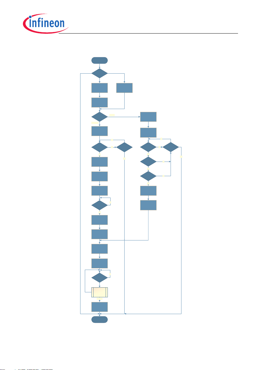
4.2 Phase I for UART BSL: Automatic serial synchronization to the host
Upon entering UART BSL mode, a serial connection is established and the transfer
speed (baud rate) of the serial communication partner (host) is automatically
synchronized in the following steps, a simplified entry flow is depicted in Figure 4-1:
• STEP 1: Initialize serial interface for reception and timer for baud rate measurement
• STEP 2: Wait for test Byte (80H) from host
• STEP 3: Synchronize the baud rate to the host
• STEP 4: Send Acknowledge Byte (55
) to the host
H
• STEP 5: Enter Phase II
4.2.1 General description
The microcontroller will set the serial port of the UART1 to mode 1 (8-bit UART, variable
baud rate) for communication. Timer 2 will be set in auto-reload mode (16-bit timer) for
baud rate measurement. In the process of waiting for the test Byte (80
will start the timer on reception of the start Bit (0) and stop it on reception of the last Bit
of the test Byte (1). Then the UART BSL routine calculates the actual baud rate, sets the
PRE and BR_VALUE values and activates baud rate generator. When the
synchronization is done, the microcontroller sends back the Acknowledge Byte (55
the host. If the synchronization fails, the baud rates for the microcontroller and the host
are different, and the Acknowledge code from the microcontroller cannot be received
properly by the host. In this case, on the host side, the host software may give a message
to the user, e.g. asking the user to repeat the synchronization procedure. On the
microcontroller side, the UART BSL routine cannot judge whether the synchronization is
correct or not. It always enters phase II after sending the Acknowledge Byte. Therefore,
if synchronization fails, a reset of the microcontroller has to be invoked, to restart it for a
new synchronization attempt.
), microcontroller
H
) to
H
User Manual 20 Rev. 1.5, 2020-09-25
Page 21
TLE986x BF BootROM
BootROM
BSL Mode Start
is NAC > 0x01
(0ms) or invalid?
Start NAC timer
(Timer21)
Timer21
elapsed?*
is RxD line low
state?
no
no
Stop NAC timer
(Timer21)**
disable WDT1**
yes
Start Baudrate
detection
(Timer2)
is RxD line high
state?
no
Stop Baudrate
detection
(Timer2)
yes
Calculate baudrate
Program BaudRate
for UART1
Return
Acknowledge (0x55)
is BSL command
received?
no
Execute BSL
command
enable WDT1
Mode 3
Exit to User Mode
BSL Mode?
Program BaudRate
for UART1
to 115.2kBaud
is BSL command
received?
Get ChipID Cmd.
Received?
yes
NAD match?
yes
FastLIN
Timer21
elapsed?*
no
no
yes
yes
yes
UART BSL
Stop NAC timer
(Timer21)**
disable WDT1**
no
no
0ms
5..55ms
disable WDT1
disable Timer21
(disable NAC timer)
invalid
Setup
Hardware
(UART, LIN)
Setup
Hardware
(Timer2, UART)
Setup Timer21
(NAC timer)
*) if NAC Timer is disabled (NAC = invalid)
Timer21 will never elaps,
it always branches to ‚no‘
**) if NAC Timer is disabled (NAC = invalid)
Stop NAC timer and disable WDT1 is
skipped
FastLIN and UART BSL Mode
Figure 4-1 BSL Entry flow (simplified)
User Manual 21 Rev. 1.5, 2020-09-25
Page 22

TLE986x BF BootROM
baud
f
PCLK
16 PRE× BR_VALUE
FDSEL
32
-------------------
+
èø
æö
×
------------------------------------------------------------------------------------------------
=
baud
f
T2Nb
×
T2
--------------------
=
f
PCLK
16 PRE× BR_VALUE
FDSEL
32
-------------------
+
èø
æö
×
------------------------------------------------------------------------------------------------
f
PCLK
8
---------------
8×
T2
------------------------
=
PRE BR_VALUE
FDSEL
32
-------------------
+
èø
æö
×
T2
16
-------
=
FastLIN and UART BSL Mode
4.2.2 Calculation of BR_VALUE and PRE values
For the baud rate synchronization of the microcontroller to the fixed baud rate of the host,
the UART BSL routine waits for a test Byte (80
polling the receive port of the serial interface (P1_DATA.4/RxD Pin), the Timer 2 is
started on the reception of the start Bit (0) and stopped on the reception of the last Bit of
the test Byte (1). Hence the time recorded is the receiving time of 8 Bits (1 start Bit plus
7 least significant Bits of the test Byte). The resulting timer val ue is 16-bi t (T2). This v alue
is used to calculate the 11-bit auto-reload value (BR_VALUE stored in the BGH and BGL
SFRs), the fractional divider FDSEL and PRE, with T2PRE predefined as 011. This
calculation needs two formulas.
First, the correlation between the baud rate (baud) and the reload value (BG) depends
on the internal peripheral frequency (
f
PCLK
Second, the relation between the baud rate (baud) and the recording value of Timer 2
(T2) depends on the T2 peripheral frequency (fT2) and the number of received Bits
(f
)
T2Nb
), which has to be sent by the host. By
H
)
[4.1]
[4.2]
Combining Equation [4.1] and Equation [4.2] with N
Simplifying Equation [4.3], we get
After setting BR_VALUE, FDSEL and PRE, the baud rate generator will then be enabled,
and the UART BSL routine sends an Acknowledge Byte (55
received correctly, it will be guaranteed that both serial interfaces are working with the
same baud rate.
User Manual 22 Rev. 1.5, 2020-09-25
=8, fT2=f
b
/ 8 (T2PRE=011),
PCLK
[4.3]
[4.4]
) to the host. If this Byte is
H
Page 23

TLE986x BF BootROM
FastLIN and UART BSL Mode
4.3 Phase I for FastLIN BSL: FastLIN BSL entry sequence
Upon entering FastLIN BSL mode, there is no automatic synchronization to the host
transfer speed. The device sets the baud rate to 115.2 kBaud. Please also refer to the
simplified entry flow in Figure 4-1.
In addition, the FastLIN mode is protected against unwanted entries, i.e. because of
noise on the communication line. In order to establish a FastLIN connection, the
following sequence must be sent to the device during the active BSL connection window
(NAC).
• STEP 1: Host to send the “Get Chip ID for FastLIN BSL entry” command
• STEP 2: Device to answer with Acknowledge (55
• STEP 3: Device to answer with the Chip ID
Get Chip ID for FastLIN BSL entry is described in Chapter 4.4.2.8.
If the sequence has been passed to the device during the BSL active window and the
device has acknowledged the commands and answered with the Chip ID then the
FastLIN BSL connection is established, the NAC and the WDT1 will be disabled and the
device will wait for further FastLIN BSL commands.
)
H
4.4 Phase II: Serial communication protocol and the working modes
Once the BSL communication is established, the FastLIN or UART BSL enters Phase II,
during which it communicates with the host to select the desired working modes. The
detailed communication protocol is explained as follows: From now on, both FastLIN and
UART BSL modes share the same UART BSL protocol.
4.4.1 Serial communication protocol
The communication between the host and the UART BSL routine is done by a simple
transfer protocol. The information is sent from the host to the microcontroller in blocks.
All the blocks follow the specified block structure. The host is sending several transfer
blocks and the UART BSL routine is just confirming them by sending back single
Acknowledge or error Bytes. The microcontroller itself does not send any transfer blocks.
However, the above rule does not apply to some modes where the microcontroller might
need to send the required data to the host besides the Acknowledge or error Byte (e.g.
mode A).
User Manual 23 Rev. 1.5, 2020-09-25
Page 24

TLE986x BF BootROM
Block Type
(1 byte)
Checksum
(1 byte)
Data Area
(X bytes)
FastLIN and UART BSL Mode
4.4.1.1 Transfer block structure
A transfer block consists of three parts:
• Block Type: the type of block, which determines how the Bytes in the data area are
interpreted. Implemented block types are:
type “Header”
–00
H
–01H type “Data”
–02H type “End of Transmission” (EOT)
• Data area: A list of Bytes, which represents the data of the block. The length of data
area cannot exceed 128 Bytes for mode 0 and 2. For mode 2, the length of data area
must always be 128 Bytes. This is due to the fact that NVM is written page-wise.
• Checksum: the XOR checksum of the Block Type and data area.
The host will decide the number of transfer blocks and their respective lengths during
one serial communication process. For safety purpose, the last Byte of each transfer
block is a simple checksum of the Block Type and data area. The host generates the
checksum by XOR-ing all the Bytes of the Block Type and data area. Every time the
UART BSL routine receives a transfer block, it recalculates the checksum of the received
Bytes (Block Type and data area) and compares it with the attached checksum.
Note: If there is less than one page to be programmed to NVM, the PC host will have to
fill up the vacancies with 00
, and transfer data in the length of 128 Bytes.
H
4.4.1.2 Transfer block type
There are three types of transfer blocks depending on the value of the Block Type.
Table 4-1 provides the general information on these block types. More details will be
described in the corresponding sections later.
User Manual 24 Rev. 1.5, 2020-09-25
Page 25

TLE986x BF BootROM
FastLIN and UART BSL Mode
Table 4-1 Type of transfer block
Block Name Block Type Description
Header block 00
H
This block has a fixed length of 8 Bytes. Special
information is contained in the data area of the block,
which is used to select different working modes.
Data block 01
H
This block length depends on the special information
given in the previous header block. This block is used in
working mode 0 and 2 to transfer a portion of program
code. The program code is contained in the data area of
the block.
EOT block 02
H
This block length depends on the special information
given in the previous header block. This block is the last
block in data transmission in working mode 0 and 2. The
last program code to be transferred is in the data area of
the block.
4.4.1.3 Response codes to the host
The microcontroller communicates to the host whether a block has been successfully
received by sending out a response code. If a block is received correctly, an
Acknowledge Code (55
two possible error codes, FFH or FEH, reflecting the two possible types of fail, Block Type
or Checksum Error. A Block Type Error occurs when either a not implemented Block
Type or transfer blocks in wrong sequence are received. For example, if in working mode
0 two consecutive header blocks are received a Block Type Error is detected and a Block
Type Error (FF
) indication is returned. A Checksum Error occurs when the checksum
H
comparison on a received block fails. In such a case, the transfer is rejected and a
Checksum Error (FEH) indication is returned. In both error cases the UART BSL routine
awaits the actual block from the host again.
When program and erase operation of NVM is restricted due to enabled NVM protection,
only modes 1, 3 and some options of mode A are allowed. All other modes are blocked
and a Protection Error code (FD
protected and no programming and erasing are allowed. In this error case, the UART
BSL routine will wait for the next header block from the host again.
) is sent. In case of failure, an error code is returned. There are
H
) will be sent to host. This will indicate that NVM is
H
Table 4-2 gives a summary of the response codes to be sent back to the host by the
microcontroller after it receives a transfer block.
User Manual 25 Rev. 1.5, 2020-09-25
Page 26

TLE986x BF BootROM
FastLIN and UART BSL Mode
Table 4-2 Type of response codes
Communication status Response code to the host
Acknowledge (Success) 55
Block Type Error FF
Checksum Error FE
Protection Error FD
Combined Offset Error
H
H
H
H
0FBH only valid for Mode 0 option F0
H
(COMBOFFSETFAULT)
ID Offset Error
0FAH only valid for Mode 0 option F0
H
(IDOFFSETFAULT)
In Page Offset Error
0F9H only valid for Mode 0 option F0
H
(INPAGEOFFSETFAULT)
Table 4-3 shows a tabulated summary of the possible responses the device may
transmit following the reception of a header, data or EOT block.
Table 4-3 Possible responses for various block types
Mode Header block Data block EOT block
0 Acknowledge, Block Type
Error, Checksum Error,
Protection Error
Acknowledge, Block
Type Error, Checksum
Error
Acknowledge, Block
Type Error,
Checksum Error,
Combined/ID/InPage
offset error
1 Acknowledge, Block Type
Error, Checksum Error
2 Acknowledge, Block Type
Error, Checksum Error,
Protection Error
Acknowledge, Block
Type Error, Checksum
Error
Acknowledge, Block
Type Error,
Checksum Error
3 Acknowledge, Block Type
Error, Checksum Error
4 Acknowledge, Block Type
Error, Checksum Error,
Protection Error
User Manual 26 Rev. 1.5, 2020-09-25
Page 27
TLE986x BF BootROM
FastLIN and UART BSL Mode
Table 4-3 Possible responses for various block types (cont’d)
Mode Header block Data block EOT block
6 Acknowledge, Block Type
Error, Checksum Error,
Protection Error
A Acknowledge, Block Type
Error, Checksum Error,
Protection Error
The responses are defined in Table 4-4, which lists the possible reasons and/or
implications for error and suggests the possible corrective actions that the host can take
upon notification of the error.
Table 4-4 Definitions of responses
Response Value Description
Acknowledge
55
Block
Type
Header1, 3 The requested operation will
H
BSL
Mode
Reasons / Implications Corrective
Action
be performed once the
response is sent.
A The requested operation has
been performed and was
successful. Requested data
transmission follows.
6 The requested operation has
EOT 0, 2, 4
All other
combinations
been performed and was
successful.
Reception of the block was
successful. Ready to receive
the next block.
Block Type
Error
FF
Header2, 4, A Start Address in Mode Data is
H
not within NVM address
Retransmit a valid
header block.
range or invalid 100TP Page.
All other
combinations
Either the Block Type is
undefined or option is invalid
Retransmit a valid
block
or the flow is invalid.
Checksum
Error
FE
H
All
combinations
There is a mismatch between
the calculated and the
Retransmit a valid
block
received Checksum.
User Manual 27 Rev. 1.5, 2020-09-25
Page 28

TLE986x BF BootROM
FastLIN and UART BSL Mode
Table 4-4 Definitions of responses (cont’d)
Response Value Description
Protection
Error
FD
Block
Type
Header0, 2,
H
BSL
Mode
4, 6, A
Reasons / Implications Corrective
Action
Protection against external
Disable protection
access enabled, i.e. userpassword is valid.
Combined
Offset
Error Code
FB
EOT 0 The operation is targeting
H
100-TP page 1 and there is at
least 1 Byte with a not in page
Check the Byte
offset.
offset and 1 byte pointing to
the Customer_ID reserved
region.
ID Offset
Error Code
FA
EOT 0 The operation is targeting
H
100-TP page 1 and there is at
Check the Byte
offset.
least 1 Byte pointing to the
Customer_ID reserved
region.
Combined
Offset
F9
EOT 0 There is at least 1 Byte with a
H
not in page offset.
Check the Byte
offset.
Error Code
4.4.1.4 Block response delay
As described in Section 4.4.1.3, after receiving any block the microcontroller
communicates to the host whether the block was successfully received by sending out
a response code. If a block is received correctly, an Acknowledge Code (55H) is sent. In
case of failure, an error code is returned.
The response is transmitted with a delay that depends on the selected mode and on the
type of the block received.
The following Table 4-5 reports the maximum response delay for each mode and block
type.
User Manual 28 Rev. 1.5, 2020-09-25
Page 29

TLE986x BF BootROM
FastLIN and UART BSL Mode
Table 4-5 Maximum Response Delay
Max Response Delay Table
Block Type
Mode Option Description Header Data EoT
Mode 0 0x00 Download Code/
250 us 1 µs per Byte 1 µs per Byte
Data to RAM
0xF0 Download data to
250 µs 1 µs per Byte 10 ms
100TP pages
Mode 1 -- RAM code
250 µs -- --
execution
Mode 2 -- Download Code/
250 µs 10 ms
1)
10 ms
Data to NVM
Mode 3 -- NVM code
250 µs -- --
execution
Mode 4 0x00 NVM page erase 4.5 ms -- --
0x40 NVM sector erase 4.5 ms -- --
0xC0 NVM mass erase 4.5 ms per
-- --
sector
Mode 6 -- NVM Protection set 10 ms
-- NVM Protection
reset
4.5 ms + 4.5
ms per sector
1)
-- --
-- --
1)
1)
Mode A 0x00 Get Chip ID 250 µs -- --
0x10 NVM Page
250 µs -- --
Checksum Check
0x18 NVM Mass
100 ms -- --
checksum check
0x50 100TP page
250 µs -- --
Checksum Check
0xC0 NVM Page 250 µs -- --
0xF0 100TP page 250 µs -- --
1)
Time needed for data collection, OpenAB, erasing old data (if required) and programming the data given
User Manual 29 Rev. 1.5, 2020-09-25
Page 30
TLE986x BF BootROM
Block Type
00
H
(Header Block)
Mode
(1 byte)
Mode Data
(5 bytes)
Checksum
(1 byte)
Data Area
FastLIN and UART BSL Mode
4.4.2 UART BSL Modes
When the UART BSL routine enters Phase II, it first waits for an 8-byte long header block
from the host. The header block contains the information for the selection of the working
modes. Depending on this information, the UART BSL routine selects and activates the
desired working mode. If the microcontroller receives an incorrect header block, the
UART BSL routine sends, instead of an Acknowledge code, a Checksum or Block Type
Error code to the host and awaits the header block again. In this case the host may react
by re-sending the header block or by releasing a message to the user.
4.4.2.1 Header Block
The header block is always the first transfer block to be sent by the host during one data
communication process. It contains the working mode number and special information
on the related mode (referred to as “Mode Data”). The general structure of a header
block is shown below.
Description:
• Block Type 00H: The Block Type, which marks the block as a header block
• Mode: The mode to be selected. The implemented modes are covered in Section 4
• Mode Data: Five Bytes of special information, which are necessary to activate
corresponding working mode.
• Checksum: The checksum of the header block.
4.4.2.2 Mode 0 - Code/Data download to RAM/100TP
Mode 0 is used to transfer a user program or data from the host to the RAM of the
microcontroller via serial interface. Selecting the proper mode option, this mode can be
used to transfer data into the user configuration sector pages. In this case, user has to
transfer data to the RAM in accordance with the format reported in the Table 5-12 and
after EOT block has been received, data is automatically copied with proper offset in the
target page. If NVM protection is installed, programming to RAM is not allowed.
Different options supported are:
• Option 00H: RAM download
•Option F0
The header block for this working mode has the following structure:
User Manual 30 Rev. 1.5, 2020-09-25
: RAM download and Configuration sector page programming
H
Page 31

TLE986x BF BootROM
00
H
(Header
Block)
StartAddr
High
(1 byte )
Checksum
(1 byte)
Mode Data ( 5 bytes)
00
H
(Mode 0 )
StartAddr
Low
(1 byte)
Block
Length
(1 byte )
Optio n
= 00
H
(1 byte)
Not Used
( 1 byte)
00
H
(Header
Block)
StartAddr
High
(1 byte)
Checksum
(1 b yte)
Mode Data ( 5 bytes)
00
H
(Mode 0 )
StartAddr
Low
(1 b yte)
Block
Length
(1 b yte)
Option
(1 Byte)
100TP
Page
( 1 b yte)
FastLIN and UART BSL Mode
The header block for RAM download (Option = 00H)
Mode Data Description:
Start Addr High, Low: 16-bit Start Address, which determines where to copy the
received program codes into the RAM.
Block Length: The length (number of Bytes) of the following data blocks or EOT block.
Not Used: this Byte is not used and will be ignored.
Option: Set to 00
for RAM download.
H
Note: RAM Address provided as input in mode 0 has to be considered as an offset to be
added to the standard RAM starting address of the TLE986x.
In option 00H start address can be each valid RAM offset address. Data sent in the
following data/ EOT blocks will be copied into the RAM at the specified address
(18000000H + StartAddr).
The header block for RAM download and 100TP page programming (Option = F0
H
)
Mode Data Description:
Start Addr High, Low: 16-bit Start Address, which determines where to copy the
received data in the RAM.
Block Length: The length of the following data blocks or EOT block.
100TP Page: This Byte is used to select the desired 100TP page to be programmed.
This Byte is relevant only in case option F0
is used. The 100TP page is selected
H
according to the addressing scheme reported in Figure 5-8.
Option: Set to F0H for RAM download and 100TP page programming
User Manual 31 Rev. 1.5, 2020-09-25
Page 32

TLE986x BF BootROM
01
H
(Data
Block)
Checksum
(1 byte )
Program Code
(((Block Length) - 2) bytes)
Program Code
(Last Codelength
bytes)
Not Used
(((Block Length) – 3 – (Last
Codelength)) bytes)
Last
Codelength
(1 byte)
02
H
(EOT
Block)
Checksum
(1 byte)
FastLIN and UART BSL Mode
Using this option, user can write data into the 100TP pages. In this case, data has to be
sent to the RAM according to the Table 5-12 and therefore start address has to be equal
to 18000400H. In case a different starting address is provided, the operation will result in
a Block Type Error indication. When this option is selected a proper 100TP page has to
be provided.
Note: RAM Address provided as input in mode 0 has to be considered as an offset to be
added to the standard RAM starting address of the TLE986x. So, for option F0H,
the Start Addr parameter has to be set to 0400H.
All other options will be treated as option 00H.
Note: The Block Length refers to the whole length (Block Type, data area and
checksum) of the following transfer block (data block or EOT block).
After successfully receiving the header block, the microcontroller enters mode 0, during
which the program codes are transmitted from the host to the microcontroller by data
block and EOT block, which are described as below.
The data block
Description:
Program Code: The program code has a length of ((Block Length) - 2) Byte, where the
Block Length is provided in the previous header block.
The EOT block
Description:
Last Codelength: This Byte indicates the length of the program code in this EOT block.
Program Code: The last program code to be sent to the microcontroller
Not used: The length is ((Block Length) - 3 - (Last Codelength)) Bytes.
User Manual 32 Rev. 1.5, 2020-09-25
Page 33

TLE986x BF BootROM
00
H
(Header
Block)
Checksum
(1 byte)
Mode Data ( 5 bytes)
01
H
(Mode 1 )
Not U sed
FastLIN and UART BSL Mode
When trying to program 100TP page, some special error handling is provided.
In particular, in addition to the generic error code, the UART BSL Mode 0 option F0
may
H
return:
• BLOCKFAULT indication (FFH) in case of wrong config sector page selection
• INPAGEOFFSETFAULT indication (F9H) in case at least one byte has an offset >
7EH, i.e. has a not in page offset or is targeting the page counter (refer to Table 5-12).
In this case, the program for the valid Bytes is still performed.
• IDOFFSETFAULT indication (FA
) in case at least one byte is targeting the
H
Customer_ID reserved region when programming 100TP page 1. In this case, the
program for the valid Bytes is still performed.
• COMBOFFSETFAULT indication (FB
) in case at least one byte is targeting the
H
Customer_ID reserved region when programming 100TP page 1 and at least 1 Byte
has a not in page offset or is targeting the page counter. In this case, the program for
the valid Bytes is still performed.
4.4.2.3 Mode 1 - Code Execution inside RAM
Mode 1 is used to execute a user program in the RAM of the microcontroller at the
address pointed by the RAM location 18000404H. The header block for this working
mode has the following structure:
The header block
Mode Data Description:
Not used: The five Bytes are not used and will be ignored in mode 1.
In working mode 1, the header block is the only transfer block to be sent by the host, no
further serial communication is necessary. The microcontroller will exit the UART BSL
mode, set the vector table in RAM at address 18000400
pointed by the standard reset handler (18000404
).
H
and branch to the address
H
4.4.2.4 Mode 2 - Code/Data download to NVM
Mode 2 is used to transfer a user program from the host to the NVM of the microcontroller
via serial interface. This mode is not accessible if NVM protection is installed.
The header block for this working mode has the following structure:
User Manual 33 Rev. 1.5, 2020-09-25
Page 34

TLE986x BF BootROM
00
H
(Header
Block)
StartAddr
4
(MSB)
Checksum
(1 byte)
Mode Data ( 5 bytes)
02
H
(Mode 2 )
StartAddr
3
Block
Length
(1 byte)
StartAddr 2StartAddr
1
(LSB)
01
H
(Data
Block)
Checksum
(1 byte)
Program Codes
(((Block Length) - 2) bytes)
FastLIN and UART BSL Mode
The header block
Mode Data Description:
Start Addr 4, 3, 2, and 1: 32-bit Start Address, which determines where to copy the
received program codes in the NVM. This address must be aligned to the page address
(Bit[6:0] = 0).
Block Length: The length of the following data blocks or EOT block. If data blocks are
to be sent, the block length has to be 130 (128+2) Bytes. If only EOT block is sent, the
block length has to be 131 (128+3) Bytes. Other block length values than 130 (data
block) or 131 (EOT block) are not allowed.
Note: If the data starts in a non-page address, PC host must fill up the beginning
vacancies with 00H and provide the start address of that page. For e.g., if data
starts in 11000F82H, the PC host will fill up the addresses 11000F80H and
11000F81H with 00H and provide the Start Address 11000F80H to
microcontroller. Moreover, if data is only 8 Bytes, the PC host will also fill up the
remaining addresses with 00
and transfer 128 data Bytes.The Block Length
H
refers to the whole length (Block Type, data area and Checksum) of the following
transfer block (data block or EOT block).
After successfully receiving the header block, the microcontroller enters mode 2, during
which the program codes are transmitted from the host to the microcontroller by data
block and EOT block, which are described as below.
The data block
Description:
Program Codes: The program codes have a length of ((Block Length) - 2) Bytes,
where Block Length is provided in the previous header block.
User Manual 34 Rev. 1.5, 2020-09-25
Page 35

TLE986x BF BootROM
Last
Codelength
(1 byte)
02
H
(EOT
Block)
Checksum
(1 byte)
Program Code
(Last Codelength
bytes)
Not Used
(((Block Length) – 3 – (Last
Codelength)) bytes)
FastLIN and UART BSL Mode
The EOT block
Description:
Last Codelength: This Byte indicates the number of program code bytes in this EOT
block.
Program Code: The last program code bytes to be sent to the microcontroller
Not used: The length is ((Block Length) - 3 - (Last Codelength)) Bytes.
The following Figures show examples of how to program one or several NVM pages
using working mode 2.
User Manual 35 Rev. 1.5, 2020-09-25
Page 36

TLE986x BF BootROM
00
H
(Header
Block)
11
H
(StartA ddr 4)
Checksum
(1 b yte)
Mode Data ( 5 bytes)
02
H
(Mode 2 )
00
H
(StartA ddr 3)
83
H
(Block Length )
00
H
(Start Addr 2)
80
H
(Start Addr 1)
80
H
(Last
Codel Ength)
02
H
(EOT
Block)
Checksum
(1 b yte)
Program Code
(128 bytes)
Host TLE98xx
Wait for Ack : Max waiting time 250 µs
55
H
(Ack)
Wait for Ack: Max waiting time 10 ms
55
H
(Ack)
FastLIN and UART BSL Mode
Figure 4-2 Single NVM Page program via working mode 2
User Manual 36 Rev. 1.5, 2020-09-25
Page 37

TLE986x BF BootROM
00
H
(Header
Block)
11
H
(StartAddr 4)
Checksum
(1 byte )
Mode Data ( 5 bytes)
02
H
(Mode 2 )
00
H
(StartAddr 3)
82
H
(Block Length )
00
H
(StartAddr 2 )
80
H
(StartAddr 1)
Host TLE98xx
Programming second, third and fourth page of the first Linear sector : NVM addresses 11000080
H
to 1100017F
H
Wait for Ack : Max waiting time 250 µs
55
H
(Ack)
Wait for Ack : Max wa iting ti me 250 us
55
H
(Ack)
01
H
(Data
Block)
Checksum
(1 byte)
Program Codesfor second page of first sector
(((Block Length) -2) bytes) = 128 Bytes
Wait for Ack : Max waiting time 10 ms
55
H
(Ack)
01
H
(Data
Block)
Checksum
(1 byte)
Program Codesfor third page of first sector
(((Block Length) -2) bytes) = 128 Bytes
Wait for Ack : Max waiting time 10 ms
55
H
(Ack)
01
H
(Data
Block)
Checksum
(1 byte )
Program Codesfor fourth page of first sector
(((Block Length) -2) bytes) = 128 Bytes
Wait for Ack : Max w aiting time 10 ms
55
H
(Ack)
00
H
(Last
CodelEngth )
02
H
(EOT
Block)
Checksum
(1 byte)
Not UsedByte
( 127 bytes)
FastLIN and UART BSL Mode
Figure 4-3 Multiple NVM Page program via working mode 2
User Manual 37 Rev. 1.5, 2020-09-25
Page 38

TLE986x BF BootROM
00
H
(Header
Block)
Checksum
(1 byte)
Mode Data ( 5 bytes)
03
H
(Mode 3 )
Not U sed
FastLIN and UART BSL Mode
4.4.2.5 Mode 3 - Code Execution inside NVM
Mode 3 is used to execute a user program in the NVM of the microcontroller at the
address pointed by the NVM location 11000004
. The header block for this working
H
mode has the following structure:
The header block
Mode Data Description:
Not used: The five Bytes are not used and will be ignored in mode 3.
In working mode 3, the header block is the only transfer block to be sent by the host, no
further serial communication is necessary. The microcontroller will exit the UART BSL
mode, set the vector table in NVM at the address 11000000
and jump to the address
H
pointed by the NVM location 11000004H.
Note: Jump to NVM will only occur when either (1) NVM is not protected and NVM
content at 11000004H is not FFH or (2) when NVM is protected. In all other cases,
firmware will put the device in sleep mode.
4.4.2.6 Mode 4 - NVM Erase
Mode 4 is used to erase different areas of the NVM. It supports mass erase of all the
NVM sectors, individual erase of the sectors for linear area or for non-linear area and
single page erase. This is determined by the Option Byte. This mode is not accessible if
the NVM protection is enabled.
Different options supported are:
• Option 00
• Option 40
• Option C0
: NVM page erase
H
: NVM sector erase
H
: NVM Mass erase
H
User Manual 38 Rev. 1.5, 2020-09-25
Page 39

TLE986x BF BootROM
00
H
(Header
Block)
StartAddr
4
(MSB)
Checksum
(1 byte)
Mode Data ( 5 bytes)
04
H
(Mode 4 )
StartAddr
3
Option
=00
H
(1 byte)
StartAddr 2StartAddr
1
(LSB
00
H
(Header
Block)
Checksum
(1 byte)
Mode Data ( 5 bytes)
04
H
(Mode 4 )
Option
= 40
H
(1 byte)
StartAddr
4
(MSB)
StartAddr 3StartAddr 2StartAddr
1
(LSB
00
H
(Header
Block)
Checksum
(1 byte)
Mode Data ( 5 bytes)
04
H
(Mode 4 )
Option
=C0
H
(1 byte )
Not Used
(4 bytes)
FastLIN and UART BSL Mode
The header block for NVM page erase (with Option = 00H)
Mode Data Description:
Start Addr High, Low: 32-bit Start Address, which determines which NVM page to be
erased. Address should be page aligned (Bit[6:0]=0).
Option: Set to 00
When the Option Byte = 00
for page erase
H
, this mode performs an erase of the NVM page specified
H
by the provided address.
The header block for NVM sector erase: (with Option = 40
)
H
Mode Data Description:
Start Addr High, Low: 32-bit Start Address, which determines which NVM sector to be
erased. Address should be sector aligned (Bit[11:0]=0).
Option: Set to 40
When the Option Byte = 40
for sector erase
H
, this mode performs an erase of the NVM sector specified
H
by the provided address. The time taken to erase a sector is max 4.5 ms.
The header block for NVM mass erase: (with Option = C0H)
Mode Data Description:
Not used: The four Bytes are not used and will be ignored in option C0H.
User Manual 39 Rev. 1.5, 2020-09-25
Page 40

TLE986x BF BootROM
00
H
(Header
Block)
User-
password
(1 byte)
Checksum
(1 byte)
Mode Data ( 5 bytes)
06
H
(Mode 6 )
Not Used
(4 bytes)
FastLIN and UART BSL Mode
Option: Set to C0H for mass erase
When the Option Byte = C0
, this mode performs a mass erase of all the NVM sectors.
H
The time taken will be max. 4.5 ms * number of sectors, as the erase operation is done
sequentially.
Note:
1. In mode 4, a Block Type Error will be sent, if an invalid option Byte is received. Once
password is set, no access to mode 4 is allowed and Protection Error will be sent.
2. NAC and NAD values will also be erased and the device will no longer be accessible
in UART BSL, because NAC is invalid and default NAC will be used.
4.4.2.7 Mode 6 - NVM Protection
Mode 6 is used to enable or disable the NVM Protection Mode by the given userpassword. The header block for this working mode has the following structure:
The header block
Mode Data Description
User-password: This Byte is given by user to enable or disable NVM protection mode.
Not used: The four Bytes are not used and will be ignored in mode 6.
In mode 6, the header block is the only transfer block to be sent by the host. If device is
unprotected, the provided user-password will be set as NVM_PASSWORD and
internally stored. No further commands will be accepted until a power up or hardware
reset. Afterwards, protection mode will be enabled.
However, if the NVM is already protected, the microcontroller will deactivate the
Protection and erase the NVM if the user-password Byte matches the stored
NVM_PASSWORD Byte. If MSB of the NVM_PASSWORD is 0, only NVM Linearly
mapped sectors are erased. If the Bit is 1, both NVM Linearly and Non-linearly mapped
regions are erased. No further commands will be accepted until a power up or hardware
reset. Afterwards, protection mode will be disabled.
User Manual 40 Rev. 1.5, 2020-09-25
Page 41

TLE986x BF BootROM
00
H
(Header
Block)
Checksum
(1 byte)
Mode Data ( 5 bytes)
0A
H
(Mode A )
Not Used
(4 bytes)
Option
=00
H
(1 byte )
FastLIN and UART BSL Mode
In case NVM is protected and the given user-password does not match the stored
NVM_PASSWORD, no actions will be triggered and a Protection Error (FDH) will be
returned instead of Acknowledge.
Note:
1. Password value has to be different from 00
either 00
or FFH on an unprotected device, the protection will not be set and a
H
and FFH. If NVM_PASSWORD is set to
H
protection error (FDH) will be returned.
2. When disabling NVM protection, together with NVM, the NAC and NAD values are
erased too. As a result, after next reset, default NAD will be used and chip waits
forever for the first FastLIN BSL frame.
Table 4-6 Erase NVM during unprotection
NVM_PASSWORD Bit 7 Description
0 Only linearly mapped NVM is erased.
1 Both linearly and non-linearly mapped NVM are erased.
4.4.2.8 Mode A - NVM Readout, Chip ID, Checksum, FastLIN BSL entry
command
Mode A is used to get 4 Bytes Chip ID data, NVM or 100TP page read, NVM or 100TP
page or NVM mass checksum check depending on the Option Byte value in the header
block.
In addition, the get Chip ID command is used as entry command for the FastLIN BSL
mode.
Different options are supported:
• Option 00
• Option 10H: NVM page checksum check
• Option 18
• Option 50
• Option C0H: NVM page read
•Option F0
: Get 4 Bytes Chip ID
H
: Mass NVM checksum check
H
: 100TP page checksum check
H
: 100TP page read
H
The header block for Get 4 Byte Chip ID (Option = 00
User Manual 41 Rev. 1.5, 2020-09-25
H
)
Page 42

TLE986x BF BootROM
00
H
(Header
Block)
Checksum
(1 byte)
Mode Data ( 5 bytes)
0A
H
(Mode A )
Opt ion
=00
H
(1 byte)
`L´
=4C
H
(1 byte)
`S´
=53
H
(1 byte)
´B`
=42
H
(1 byte)
NAD
(1 byte)
BSL Entry Key
FastLIN and UART BSL Mode
Mode Data Description:
Not Used: These Bytes are not used and will be ignored for Option 00
.
H
Option: Set to 00H for Get 4 Byte Chip ID.
If this command is successfully received, microcontroller will return an Acknowledge
followed by 4 data Bytes and a single byte checksum. The order of the 4 Bytes of data
are SFR ID, CHIP_ID2, CHIP_ID1 and CHIP_ID0. Refer to Chapter 5.2.1 for CHIP_ID
definition.
Note: The checksum is calculated on the acknowledge and the 4 data bytes.
The header block for Get 4 Byte Chip ID as FastLIN entry (Option = 00
)
H
In order to avoid unwanted entries, the FastLIN connection is established only if this
command is successfully received during the active BSL connection window defined by
the NAC. This command must then be the first FastLIN BSL command to be sent by the
Host.
Mode Data Description:
NAD: Node Address for Diagnostic, specifies the address of the active slave node. See
Chapter 3.1.9.
BSL Entry Key: “BSL” in ASCII.
Option: Set to 00
for Get 4 Byte Chip ID.
H
If this command is successfully received, the microcontroller returns an Acknowledge
followed by 4 data Bytes and a single byte checksum. The order of the 4 Bytes of data
are SFR ID, CHIP_ID2, CHIP_ID1 and CHIP_ID0. Refer to Chapter 5.2.1 for CHIP_ID
definition.
On successful completion of the sequence, FastLIN BSL is fully entered and all other
commands can be executed.
Note: The checksum is calculated on the acknowledge and the 4 data bytes.
User Manual 42 Rev. 1.5, 2020-09-25
Page 43

TLE986x BF BootROM
00
H
(Header
Block)
StartAddr
High
(1 byte)
Checksum
(1 byte)
Data Area
0A
H
(Mode A )
StartAddr
Low
(1 byte)
Option
=10
H
(1 byte )
Expected
CHKSum
High
(1 byte)
Expected
CHKSum
Low
(1 byte)
FastLIN and UART BSL Mode
The header block for NVM page checksum check (Option = 10H)
Mode Data Description:
Start Addr High, Low: Address of the NVM page for checksum check. (Address should
be page aligned, Bit[6:0]=0).
Expected CHKSum High, Low: Expected checksum High/Low Byte.
Option: set to 10
to enable NVM page checksum check.
H
Note: The start address provided with the header block must be shifted by 7 bits to the
left and then added to the NVM start address to build the actual address, i.e. it is
calculated as follows in Mode A Option C0H: Actual address = 11000000H +
(StartAddrHigh << 15) + (StartAddrLow << 7).
This option will trigger a checksum calculation (16 bits inverted XOR, refer to
Chapter 4.4.3) over the whole page pointed by the address given in the header block
and the result will then be compared with the expected checksum (provided as well by
the user in the header frame). If the given address is a valid NVM address, the
microcontroller will return an Acknowledge followed by four data Bytes and a single byte
checksum. The Bytes are, in sequential order, pass/fail indication (00
and expected checksum match, 80
if they differ), calculated checksum High Byte,
H
if the calculated
H
calculated checksum Low Byte, and a final Byte equal to 00H.
Note: The checksum is calculated on the acknowledge and the 4 data bytes.
The input address should always be page aligned. In case it is not aligned, the address
will be internally changed to point to the beginning of the addressed page so that
checksum is always evaluated on a complete page.
In case the provided address is not a valid NVM address, the microcontroller will return
a Block Type Error (FF
) instead of an Acknowledge (55H) followed by no further Bytes.
H
Note: In case the address is pointing to an erased non linearly mapped page, the
address is considered invalid and a Block Type Error (FFH) is returned.
User Manual 43 Rev. 1.5, 2020-09-25
Page 44

TLE986x BF BootROM
00
H
(Header
Block)
Checksum
(1 byte)
Mode Data ( 5 bytes)
0A
H
(Mode A )
Option
=18
H
(1 byte )
Expected
CHKSum
High
(1 byte)
Expected
CHKSum
Low
(1 byte)
Not Used
(1 byte)
Not Used
(1 byte )
00
H
(Header
Block)
Checksum
(1 byte)
Data Area
0A
H
(Mode A )
Option
=50
H
(1 byte)
Expected
CHKSum
High
(1 byte)
Expected
CHKSum
Low
(1 byte)
100TP
Page
(1 byte)
Not Used
(1 byte )
FastLIN and UART BSL Mode
The header block for Mass checksum check (Option = 18H)
Mode Data Description:
Not Used: These Bytes are not used and will be ignored for Option 18
.
H
Expected CHKSum High, Low: Expected checksum High/Low Byte.
Option: set to 18
to enable mass checksum check.
H
This option will trigger a checksum calculation (16 bits inverted XOR, refer to
Chapter 4.4.3) over all the linearly mapped sectors (including erased pages and
sectors). The not linearly mapped sectors and 100TP pages are not included. The result
will then be compared with the expected checksum (provided by the user in the header
frame). The microcontroller will return an Acknowledge followed by four data Bytes and
a single byte checksum. The Bytes are, in sequential order, pass/fail indication (00H if
the calculated and expected checksum match, 80
if they differ), calculated checksum
H
High Byte, calculated checksum Low Byte, and a final Byte equal to 00H.
Note: The checksum is calculated on the acknowledge and the 4 data bytes.
The header block for 100TP page checksum check (Option = 50
)
H
Mode Data Description:
100TP Page: Selection of the 100TP Page to be checked (refer to Figure 5-8).
Not Used: This Byte is not used and will be ignored for Option 50
.
H
Expected CHKSum High, Low: Expected checksum High/Low Byte.
Option: set to 50
User Manual 44 Rev. 1.5, 2020-09-25
to enable 100TP page checksum check.
H
Page 45

TLE986x BF BootROM
00
H
(Header
Block)
StartAddr
High
(1 byte)
Checksum
(1 b yte)
Mode Data ( 5 bytes)
0A
H
(Mode A )
StartAddr
Low
(1 b yte)
Option
=C0
H
(1 byte )
Not Used
(1 byte)
Not Used
(1 byte)
FastLIN and UART BSL Mode
This option will trigger a checksum calculation (16 bits inverted XOR, refer to
Chapter 4.4.3) over the whole 100TP page pointed by the address given in the header
block and the result will then be compared with the expected checksum (provided as well
by the user in the header frame). The 100TP page address has to be in accordance with
the configuration sector address scheme described in the Figure 5-8. If the given
address is valid, the microcontroller will return an Acknowledge followed by four data
Bytes and a single byte checksum. The Bytes are, in sequential order, pass/fail
indication (00
if the calculated and expected checksum match, 80H if they differ),
H
calculated checksum High Byte, calculated checksum Low Byte, and a final Byte equal
.
to 00
H
In case the provided address is not valid, the microcontroller will return a Block Type
Error (FFH) instead of an Acknowledge (55H) followed by no further Bytes.
Note: The checksum is calculated on the acknowledge and the 4 data bytes.
The header block for NVM page read (Option C0
)
H
Mode Data Description:
Start Addr High, Low: Address of the NVM page to be read (Address should be page
aligned, Bit[6:0]=0).
Not Used: These Bytes are not used and will be ignored for Option C0
H
Option: set to C0H to enable NVM page read.
Note: The start address provided with the header block has to be shifted by 7 bits to the
left and then added to the NVM start address to build the actual address, i.e. it is
calculated as follows in Mode A Option C0H: Actual address = 11000000H +
(StartAddrHigh << 15) + (StartAddrLow << 7).
This option will trigger a read of the addressed NVM page. Microcontroller will return an
Acknowledge (55H) followed by the 128 NVM page data Bytes (starting from the least
significant Byte of the page).
User Manual 45 Rev. 1.5, 2020-09-25
.
Page 46

TLE986x BF BootROM
00
H
(Header
Block)
Checksum
(1 byte)
Mode Data ( 5 bytes)
0A
H
(Mode A )
Option
=F0
H
(1 byte)
Not Used
(1 byte)
100TP
Page
(1 byte)
Not Used
(1 byte)
Not Used
(1 byte)
FastLIN and UART BSL Mode
The input address should always be aligned with a page. In case it is not aligned, the
address will be internally changed to point to the beginning of the addressed page so
that the page Bytes are always returned ordered from the least to the most significant
Byte.
In case the provided address is not a valid NVM address, the microcontroller will return
a Block Type Error (FFH) instead of an Acknowledge (55H) followed by no further Bytes.
To prevent user code to be read, this option is disabled if NVM is protected and only a
Protection Error Byte (FDH) will be returned.
Note: In case the address is pointing to an erased non linearly mapped page, the
address is considered invalid and a Block Type Error (FFH) is returned.
The header block for 100TP page read (Option = F0
)
H
Mode Data Description:
Not Used: These Bytes are not used and will be ignored for Option F0
.
H
100TP Page: Selection of the 100TP Page to be checked (refer to Figure 5-8).
Option: set to F0
to enable 100TP page read.
H
This option will trigger a read of the addressed 100TP page. Microcontroller will return
an Acknowledge (55
) followed by the 128 100TP page data Bytes (starting from the
H
least significant Byte of the page).
The 100TP page is selected by the CS Page Byte according to the scheme shown in
Figure 5-8.
In case an invalid 100TP page is selected the microcontroller will return a Block Type
Error (FFH) instead of an Acknowledge (55H) followed by no further Bytes.
To prevent user code to be read, this option is disabled if NVM is protected (NVM
password installed) and only a Protection Error Byte (FD
) will be returned.
H
All other values for option Byte
Block Type Error indication (FF
User Manual 46 Rev. 1.5, 2020-09-25
) is sent back.
H
Page 47

TLE986x BF BootROM
Byte(0) Byte(n-2) Byte( n-1)Byte (1) Byte (2) Byte (3) Byte (4) Byte (5)
HalfWord(0) HalfWord(1) HalfWord(2) HalfWord((n-2)/2)
~( HW(0) xor HW(1) xor HW(2) xor ---------------------------------------- xor HW((n-2)/2) )
For a NVM page, n= 128 =>
~( HW(0) xor HW(1) xor HW(2) xor ----------------------------------------- xor HW(63) )
FastLIN and UART BSL Mode
In mode A, the header block is the only transfer block to be sent by the host. The
microcontroller will return an Acknowledge followed by data Bytes if the header block is
received successfully. If an invalid option is received, the microcontroller will return a
Block Type Error indication (FF
) and no further Bytes.
H
4.4.3 16 bits inverted XOR checksum
This checksum structure is used in BSL Mode A options 10H, 18H, 50H as a fast data
integrity check. These modes will read the specified NVM range, calculate the checksum
and compare it against the expected one provided as command parameter.
To calculate this checksum, all Half-Words (16 bits) of the selected NVM region are
xored. The resulting value is then logically complemented (1´s complement).
The following figure shows the calculation algorithm.
Figure 4-4 16 bits inverted XOR checksum calculation
4.5 WDT1 refreshing
After a reset the WDT1 is starting with a long open window. WDT1 keeps on running
while waiting for first UART frame. In case during the UART BSL waiting time, defined
by NAC, a UART communication is detected, WTD1 is disabled and its status frozen.
Subsequently, before exiting to RAM or NVM in UART BSL modes 1 and 3 the watchdog
is re-enabled and starts from the previously frozen state. The WDT1 is then still in long
open window and the remaining valid time is equal to long open window minus the time
between reset release and first UART communication. User program needs to trigger the
WDT1 refresh accordingly.
User Manual 47 Rev. 1.5, 2020-09-25
Page 48

TLE986x BF BootROM
NVM
5NVM
Non Volatile Memory (NVM) is the flash module of the TLE986x which partly supports
EEPROM emulation.
5.1 NVM overview
The NVM is a single block of NVM memory of up to 256 kBytes separated into Code and
Data space. The following table shows the NVM address range.
Table 5-1 NVM address range
Address Address Range
NSA to NEA NVM memory
NSA and NEA values are shown in Table 5-2:
Table 5-2 NVM Size and Address Range
NVM Size
(kB)
36 11000000
64 11000000HF000
128 11000000H1F000
256 11000000H3F000
NVM
Starting
Address
(NSA)
NVM Linear
Size, NVM
CFLASH Size
(NLS)
8000
H
NVM
DFLASH
Starting
Address
NVM
DFLASH
Size
NVM DFLASH
End Address,
NVM FLASH
End Address
(NEA)
H
H
H
H
11008000H1000
1100F000H1000
1101F000H1000
1103F000H1000
H
H
H
H
11008FFF
1100FFFF
1101FFFF
1103FFFF
H
H
H
H
Note: An erased page is ECC-Clean and will not generate an ECC error.
Note: Reading an erased page in the Code space will return FF
and will not trigger any
H
error.
Note: Reading an erased page in the Data space will return 00H and will also create an
NVM Map Error NMI, if enabled in NMICON. As a consequence, an erased page
in the Data space has to be written before it can be read without triggering an error.
5.1.1 NVM organisation
The NVM has 2 types of memory configuration, Code and Data. It is organised in sectors.
Each NVM Sector is a block of 4 kBytes organised into blocks of 128 Bytes called Page.
The page is the minimum data granularity for NVM (code and data) write and erase so,
with this NVM structure, any NVM update, even when targeting only one byte, actually
User Manual 48 Rev. 1.5, 2020-09-25
Page 49

TLE986x BF BootROM
NVM
involves 128 bytes. Table 5-3 shows the sector address organisation of the first and last
4 sectors of the 256 kBytes NVM. The other sector organization can be simply derived
per extension of the reported scheme. Table 5-4 shows the page address organisation
of NVM Sector 1 and it can be used as a reference for page organization of any NVM
Sector.
Table 5-3 NVM memory sector organisation
Address NVM Sector Number
11000000H to
1
11000FFFH
11001000H to
2
11001FFFH
11002000H to
3
11002FFFH
11003000H to
4
11003FFFH
1103C000H to
61
1103CFFFH
1103D000H to
62
1103DFFFH
1103E000H to
63
1103EFFFH
1103F000H to
64
1103FFFFH
Table 5-4 NVM memory sector 1 page organisation
Address Page Number of NVM Sector
11000000H to
0
1100007FH
11000080H to
1
110000FFH
11000100H to
2
1100017FH
11000180H to
3
110001FFH
11000200H to
4
1100027FH
User Manual 49 Rev. 1.5, 2020-09-25
Page 50

TLE986x BF BootROM
Table 5-4 NVM memory sector 1 page organisation (cont’d)
Address Page Number of NVM Sector
11000280H to
5
110002FFH
11000300H to
6
1100037FH
11000380H to
7
110003FFH
11000400H to
8
1100047FH
11000480H to
9
110004FFH
11000500H to
10
1100057FH
11000580H to
11
110005FFH
11000600H to
12
1100067FH
11000680H to
13
110006FFH
11000700H to
14
1100077FH
11000780H to
15
110007FFH
11000800H to
16
1100087FH
11000880H to
17
110008FFH
11000900H to
18
1100097FH
11000980H to
19
110009FFH
11000A00H to
20
11000A7FH
11000A80H to
21
11000AFFH
NVM
User Manual 50 Rev. 1.5, 2020-09-25
Page 51

TLE986x BF BootROM
Table 5-4 NVM memory sector 1 page organisation (cont’d)
Address Page Number of NVM Sector
11000B00H to
11000B7FH
11000B80H to
11000BFFH
11000C00H to
11000C7FH
11000C80H to
11000CFFH
11000D00H to
11000D7FH
11000D80H to
11000DFFH
11000E00H to
11000E7FH
11000E80H to
11000EFFH
11000F00H to
11000F7FH
11000F80H to
11000FFFH
22
23
24
25
26
27
28
29
30
31
NVM
5.2 NVM configuration sectors organisation
The configuration sector contains important user data needed for proper system
initialization.
5.2.1 Chip ID definition
The specific characteristics of the different variants of the product family are captured in
the definition of the CHIP_ID Bytes.
The Chip_ID bytes can be read via BSL mode A. When triggered, this mode replies
providing the 3 CHIP_ID Bytes plus the content of the Identification Register (ID).
Please refer to the following tables for CHIP_ID details. This is a variant specific
identification number. The unique device specific identification number is described in
Table 5-11.
User Manual 51 Rev. 1.5, 2020-09-25
Page 52

TLE986x BF BootROM
Table 5-5 Chip ID Byte 0
Res MAX_FREQ OP_AMP Phases DMA PKG Type
Table 5-6 Chip ID Byte 0 Bits Description
Field Bits Description
PKG_Type [1:0] Package Type
00 VQFN-48
01 TQFP-48
10 Reserved
11 Reserved
DMA 2 DMA
0 with DMA
1 without DMA
Phases 3 Bridge driver number of phases
0 2 phases
1 3 phases
OP_AMP 4 Op Amp
0 with Op Amp
1 without Op Amp
Max Freq [6:5] Maximum Frequency
00 reserved
01 20 MHz
10 24MHz
11 40 MHz
Res 7 Reserved
NVM
Table 5-7 Chip ID Byte 1
NVM_SIZE
User Manual 52 Rev. 1.5, 2020-09-25
EEPROM_SIZE
Page 53

TLE986x BF BootROM
Table 5-8 Chip ID Byte 1 Bits Description
Field Bits Description
EEPROM_SIZE [3:0] EEPROM (non-linearly mapped NVM) Size
0000 0 Kbyte
0001 4 Kbyte
0010 8 Kbyte
0011 12 Kbyte
0100 16 Kbyte
0101 20 Kbyte
0110 24 Kbyte
0111 28 Kbyte
1000 32 Kbyte
1001 36 kByte
1010 40 Kbyte
1011 44 Kbyte
1100 48 Kbyte
1101 52 Kbyte
1110 56 Kbyte
1111 60 Kbyte
NVM_SIZE [7:4] total NVM Size
0000 Res
0001 256 Kbyte
0010 Res
0011 36 Kbyte
0100 Res
0101 Res
0110 Res
0111 64 Kbyte
1000 Res
1001 Res
1010 Res
1011 Res
1100 Res
1101 Res
1110 Res
1111 128 Kbyte
NVM
Table 5-9 Chip ID Byte 2
Res VARIANT_ID
User Manual 53 Rev. 1.5, 2020-09-25
Page 54

TLE986x BF BootROM
NVM
Table 5-10 Chip ID Byte 2 Bits Description
Field Bits Description
VARIANT_ID [3:0] Variant ID
Res [7:4] Reserved
5.2.2 100 Time Programmable data
User has eight 100 time programmable pages. The first one is used to store user
configuration parameters for measurement interface and sense amplifier as well as
ADC1 calibration parameters. These parameters are usually determined in the user
application and might require several iterations before the best fit is found.
The values of the first page, from offset 10
dedicated SFR registers after every power on reset, brown out reset or wake-up reset
from sleep mode thus replacing the registers default reset values. The user can check
them by reading the dedicated SFRs or by reading directly the content of the page.
The first 4 Bytes of the first 100TP page are used to store a device ID that can be read
by the user. The content of these 4 bytes are preloaded prior to shipment and cannot be
modified by the user. In case the user tries to write these values via the 100TP page
writing features offered in BSL or via NVM user routine, an error is reported and the
original content of the bytes is preserved. The Customer_ID definition is described in
Figure 5-1.
The data stored in this first 100 time programmable page can be found in Table 5-11.
To read data stored in the 100TP pages, refer to Section 5.3.11.
To perform the programming of these pages, the user is required to preload the contents
to be programmed into the RAM as listed in Table 5-12. The offset entered for the
programming does not need to be in sequential order. Once a page has been
programmed 100 times, no further programming on that page is allowed. In the last Byte
of each 100TP page a program counter is stored (not changeable by user).
Since part of the data stored in the first 100TP page are used as trim or configuration
data at reset, the content is protected by an in-page checksum (XOR of the first 126
bytes of the page) stored at one before last byte of the page (in-page offset 7E
Table 5-11). User is required to properly calculate and update the checksum when re-
programming the 100TP page 1.
Note: At power on reset, brown out reset or wake-up reset from sleep mode, the
firmware checks the checksum of the first 100TP page. In case the
checksum is not correct, The data stored from offset 10
downloaded into the SFRs and backup values are used instead.
For further information regarding 100TP page program, refer to Section 5.3.12.
to 63H, are automatically copied into the
H
, refer to
H
to 63H are not
H
User Manual 54 Rev. 1.5, 2020-09-25
Page 55

TLE986x BF BootROM
Table 5-11 100-Time Programmable Page 1
Data
Offset
00H to
03
04
SFR / Variable
Description Default
Name
CUSTOMER_ID Device ID for user Device ID
H
GAIN_VS_10B Calibration gain for supply
H
voltage measurement
05
OFFSET_VS_10B Calibration offset for supply
H
voltage measurement
06
07
08
GAIN_VBAT_SENS
H
E_10B
OFFSET_VBAT_SE
H
NSE_10B
GAIN_VMON_ATT_
H
1_5
Calibration gain for battery
voltage measurement
Calibration offset for battery
voltage measurement
Calibration gain for high
voltage monitoring input
voltage measurement
09
OFFSET_VMON_A
H
TT_1_5
Calibration offset for high
voltage monitoring input
voltage measurement
0A
0B
0C
0D
0E
0F
10
13
14
17
18
1B
CONFIG_VERS Configuration Sector version 02
H
Reserved Reserved 00
H
to
CFLASH_PW Linearly mapped region
H
H
to
DFLASH_PW Non-Linearly mapped region
H
H
to
MEAS_ADC2_CTRL1Measurement unit:
H
H
to
MEAS_ADC2_CTRL2Measurement unit:
H
H
to
MEAS_ADC2_SQ1_4Channel controller:
H
H
protection removal password
protection removal password
Control register 1
Control register 2
Measurement channel
enable Bits of cycle 1 to 4
1CH to
1F
MEAS_ADC2_SQ5_8Channel controller:
H
Measurement channel
enable Bits of cycle 5 to 8
NVM
Back-up
Value
Value
1)
N.A.
dependent
Chip
N.A.
Individual
Chip
N.A.
Individual
Chip
N.A.
Individual
Chip
N.A.
Individual
Chip
N.A.
Individual
Chip
N.A.
Individual
H
H
0000
0000
H
H
N.A.
N.A.
N.A.
N.A.
00000000H00000000
H
00000703H00000703
H
29362837H29362837
H
28372836H28372836
H
User Manual 55 Rev. 1.5, 2020-09-25
Page 56

TLE986x BF BootROM
Table 5-11 100-Time Programmable Page 1 (cont’d)
Data
Offset
20H to
23
SFR / Variable
Description Default
Name
MEAS_ADC2_SQ9_10Channel controller:
H
Measurement channel
enable Bits of cycle 9 to 10
24
to
ADC2_CAL_CH0_1 Calibration unit:
H
27
H
Calibration of channel 0 and
1
28
to
ADC2_CAL_CH2_3 Calibration unit:
H
2B
H
Calibration of channel 2 and
3
2CH to
2F
ADC2_CAL_CH4_5 Calibration unit:
H
Calibration of channel 4 and
5
30
to
ADC2_FILTCOEFF0_5IIR filter:
H
33
H
Filter coefficients of ADC
channels 0 to 5
34
to
ADC2_FILT_UP_CTRLPostprocessing:
H
37
38
3B
3C
3F
H
to
ADC2_FILT_LOW_
H
CTRL
H
to
ADC2_TH0_3_LOWERPostprocessing:
H
H
Upper threshold filter enable
Postprocessing:
Lower threshold filter enable
Lower comparator trigger
level of channels 0 to 3
40H to
43
ADC2_TH4_5_LOWERPostprocessing:
H
Lower comparator trigger
level of channels 4 to 5
44
to
ADC2_TH6_9_LOWERPostprocessing:
H
47
H
Lower comparator trigger
level of channels 6 to 9
48H to
4B
ADC2_TH0_3_UPPERPostprocessing:
H
Upper comparator trigger
level of channels 0 to 3
4CH to
4F
ADC2_TH4_5_UPPERPostprocessing:
H
Upper comparator trigger
level of channels 4 to 5
NVM
Back-up
Value
Value
1)
00002936H00002936
H
Chip
Individual
Chip
Individual
Chip
Individual
Chip
Individual
Chip
Individual
Chip
Individual
00000AAAH00000AAA
H
00000F3FH00000F3F
H
00000F3FH00000F3F
H
182F423AH182F423A
H
00009A00H00009A00
H
C6D39EC
D
H
ABBDC5C
0
H
C6D39EC
D
H
ABBDC5C
0
H
0000BC00H0000BC00
H
User Manual 56 Rev. 1.5, 2020-09-25
Page 57

TLE986x BF BootROM
Table 5-11 100-Time Programmable Page 1 (cont’d)
Data
Offset
50H to
53
SFR / Variable
Name
ADC2_CNT0_3_LO
WER
H
Description Default
Postprocessing:
Lower counter trigger level of
channels 0 to 3
54
to
57
ADC2_CNT4_5_LO
H
WER
H
Postprocessing:
Lower counter trigger level of
channels 4 to 5
58
to
5B
ADC2_CNT0_3_UP
H
PER
H
Postprocessing:
Upper counter trigger level of
channels 0 to 3
5CH to
5F
ADC2_CNT4_5_UP
PER
H
Postprocessing:
Upper counter trigger level of
channels 4 to 5
60
to
ADC2_MMODE0_5 Postprocessing:
H
63
H
Overvoltage measurement
mode of channels 0 to 5
64
to
Reserved Reserved 00
H
6B
6C
6D
6E
6F
70
71
72
73
H
CHIP_ID_BYTE_00 Chip Id Byte 00
H
CHIP_ID_BYTE_01 Chip Id Byte 01
H
CHIP_ID_BYTE_02 Chip Id Byte 02
H
CHIP_ID_BYTE_03 Chip Id Byte 03
H
CHIP_ID_BYTE_04 Chip Id Byte 04
H
CHIP_ID_BYTE_05 Chip Id Byte 05
H
CHIP_ID_BYTE_06 Chip Id Byte 06
H
CHIP_ID_BYTE_07 Chip Id Byte 07
H
2)
2)
2)
2)
2)
2)
2)
2)
NVM
Back-up
Value
Value
1)
12131312H12131312
H
00000A0AH00000A0A
H
12131B1AH12131B1A
H
00001212H00001212
H
00000000H00000000
H
H
Chip
N.A.
N.A.
Individual
Chip
N.A.
Individual
Chip
N.A.
Individual
Chip
N.A.
Individual
Chip
N.A.
Individual
Chip
N.A.
Individual
Chip
N.A.
Individual
Chip
N.A.
Individual
User Manual 57 Rev. 1.5, 2020-09-25
Page 58

TLE986x BF BootROM
Table 5-11 100-Time Programmable Page 1 (cont’d)
Data
Offset
74
75
76
77
78
SFR / Variable
Name
CHIP_ID_BYTE_08 Chip Id Byte 08
H
CHIP_ID_BYTE_09 Chip Id Byte 09
H
CHIP_ID_BYTE_10 Chip Id Byte 10
H
CHIP_ID_BYTE_11 Chip Id Byte 11
H
CS_SA_WITH_PRO
H
T_EN
Description Default
2)
2)
2)
2)
When set to A5H, enables
Service Algorithm even on
protected NVM Data Sector.
79
CS_USER_CAL_ST
H
ARTUP_EN
Enable Byte for user
calibration data download
during startup. If value=0xC3
then the download is enabled
7A
CS_USER_CAL_XA
H
DDH
High Byte of the RAM
starting address where
downloaded data has to be
stored(0xF0 for RAM initial
address)
7B
CS_USER_CAL_XA
H
DDL
LOW Byte of the RAM
starting address where
downloaded data has to be
stored(0x00 for RAM initial
address)
7C
CS_USER_CAL_10
H
0TP_PAGE
100TP page where
calibration data has to be
downloaded from. By default
100TP page1 should be
used (Value=0x11)
7D
CS_USER_CAL_NUMNumber of Bytes to be
H
downloaded starting from the
first Byte of the selected
100TP page.
Value
Chip
Individual
Chip
Individual
Chip
Individual
Chip
Individual
00
H
00
H
00
H
00
H
00
H
00
H
NVM
Back-up
1)
Value
N.A.
N.A.
N.A.
N.A.
N.A.
N.A.
N.A.
N.A.
N.A.
N.A.
User Manual 58 Rev. 1.5, 2020-09-25
Page 59

TLE986x BF BootROM
Table 5-11 100-Time Programmable Page 1 (cont’d)
Data
Offset
7E
7F
SFR / Variable
Name
CHECKSUM_100TP
H
_P1
PROG_TIMES_100
H
TP_P1
Description Default
Value
XOR of the first 126 Bytes of
100TP page 1.
This reflects the number of
Chip
Individual
00
H
times that this page has been
Back-up
Value
N.A.
N.A.
programmed. (Up to a
maximum of 100 times.)
1)
Values used during startup for analog module trimming in case a checksum error on 100TP page 1 is detected.
Refer to Chapter 3.1.5.
2)
This is a unique device specific identification number. The variant specific identification number is described
in Chapter 5.2.1.
Table 5-12 RAM preloading for 100 Time Programmable page programming
RAM Address Function
18000400H Number of Bytes to be programmed (i.e. N, up to a
maximum of 1271) Bytes)
18000401H 100TP offset 1
18000402
18000403
18000404
100TP data 1 to be programmed
H
100TP offset 2
H
100TP data 2 to be programmed
H
..... ....
18000401H + ((N-1) x 2) 100TP offset N
18000402
1)
The maximum number of bytes that the user can load into the 100TP pages is limited to 127 since last byte is
used as a program operation counter. To ensure that the page are not programmed more than 100 times, even
not by accident, the counter byte (last byte in the page) can be read but not overwritten by the user.
+ ((N-1) x 2) 100TP data N to be programmed
H
NVM
1)
User Manual 59 Rev. 1.5, 2020-09-25
Page 60

TLE986x BF BootROM
Family Derivative Design step Reserved
Sales code Feature
Pack CLK
Major no. Minor no.
31 24 23 20 19 16 15 12 11 8 7 0
Family
[Decimal values]
0: Reserved
1: 2-phase (TLE986x)
2: 3-phase (TLE987x)
Others: R eser ved
Derivative – Sales code
[Decimal values]
0: TLE98x0
1: TLE98x1
2: TLE98x2
3: TLE98x3:
4: TLE98x4
5: TLE98x5
6: TLE98x6
7: TLE98x7
8: TLE98x8
9: TLE98x9
others: Reserved
Derivative – Feature – Pack.
[Decimal values]
0: VQFN48QX
1: TQFP48
Others: Reserved:
Derivative – Feature – CLK
[Decimal values]
0: 20 MHz
1: 24 MHz
2: 40 MHz
3: Reserved:
Design Step (Major)
[Hex values]
A: Design Step A
B: Design Step B
Others: Reserved
Design Step (Minor)
[Hex values]
A: Design Step A
B: Design Step B
C: Design Step C
D: Design Step D
E: Design Step E
F: Design Step F
NVM
Figure 5-1 Customer_ID definition
5.3 NVM user routines organisation
The NVM user routines are BootROM routines called by user and placed from the
address 0000383DH to 00003925H. The complete list of NVM user routines can be found
in Table 5-13.
User Manual 60 Rev. 1.5, 2020-09-25
Page 61

TLE986x BF BootROM
Table 5-13 NVM user routines list
Address Routine Description
00003925
USER_CFLASH_WR_PROT_EN To enable write protection on
H
the linearly mapped NVM
sectors.
0000391D
USER_CFLASH_WR_PROT_DIS To disable write protection on
H
the linearly mapped NVM
sectors.
00003915
USER_CFLASH_RD_PROT_EN To enable read protection on the
H
linearly mapped NVM sectors.
0000390D
USER_CFLASH_RD_PROT_DIS To disable read protection on
H
the linearly mapped NVM
sectors.
00003905
USER_DFLASH_WR_PROT_EN To enable write protection on
H
the non linearly mapped NVM
sectors.
000038FD
USER_DFLASH_WR_PROT_DIS To disable write protection on
H
the non linearly mapped NVM
sectors.
000038F5
USER_DFLASH_RD_PROT_EN To enable read protection on the
H
non linearly mapped NVM
sectors.
000038ED
USER_DFLASH_RD_PROT_DIS To disable read protection on
H
the non linearly mapped NVM
sectors.
000038E5
USER_OPENAB To open the assembly buffer for
H
writing
000038DD
000038D5
000038CD
USER_PROG To program the NVM
H
USER_ERASEPG To erase an NVM page
H
USER_ABORTPROG To abort the NVM programming
H
by closing the assembly buffer
000038C5
USER_NVMRDY To access if the NVM is in ready
H
to read status
000038BD
USER_READ_CAL To read the NVM calibration
H
data.
000038B5
USER_NVM_CONFIG To read the NVM configuration
H
status
NVM
User Manual 61 Rev. 1.5, 2020-09-25
Page 62

TLE986x BF BootROM
Table 5-13 NVM user routines list (cont’d)
Address Routine Description
000038AD
0000389D
00003895
0000388D
00003885
00003875
USER_NVM_ECC2ADDR To read the NVM ECC2 address
H
USER_MAPRAM_INIT To initialize MapRAM
H
USER_VERIFY_PAGE
H
1)
USER_ERASE_SECTOR_VERIFY1)To perform a sector erase verify
H
USER_ERASEPG_VERIFY
H
1)
USER_READ_100TP To read the NVM 100TP
H
To perform a page verify
To perform a page erase verify
parameter data
0000386D
USER_100TP_PROG To perform the 100TP program.
H
(This can be used 100 times per
100TP page)
00003865
USER_ERASE_SECTOR To erase an NVM Sector
H
00003855H USER_NVMCLKFAC_SET To set NVMCLKFAC Bit in
SYSCON0
0000384D
USER_RAM_MBIST_START To perform a sequential
H
checkerboard and inverted
checkerboard test on the RAM.
00003845
USER_NVM_ECC_CHECK To trigger a complete NVM read
H
and provide cumulated ECC
single bit error indication.
0000383D
USER_ECC_CHECK To provide cumulated ECC
H
single bit error indication since
last call of the function.
1)
This function is not available for variants with 256KB flash.
NVM
Table 5-14 NVM User Routines Maximum Stack Usage
Routine Maximum Stack Usage
USER_CFLASH_WR_PROT_EN 0000
USER_CFLASH_WR_PROT_DIS 0000
USER_CFLASH_RD_PROT_EN 0000
USER_CFLASH_RD_PROT_DIS 0000
User Manual 62 Rev. 1.5, 2020-09-25
H
H
H
H
Page 63

TLE986x BF BootROM
Table 5-14 NVM User Routines Maximum Stack Usage (cont’d)
Routine Maximum Stack Usage
USER_DFLASH_WR_PROT_EN 0000
USER_DFLASH_WR_PROT_DIS 0000
USER_DFLASH_RD_PROT_EN 0000
USER_DFLASH_RD_PROT_DIS 0000
USER_OPENAB 0038
USER_PROG 00B0
USER_ERASEPG 0058
USER_ABORTPROG 0010
USER_NVMRDY 0000
USER_READ_CAL 0030
USER_NVM_CONFIG 000C
USER_NVM_ECC2ADDR 000C
USER_MAPRAM_INIT 0020
USER_VERIFY_PAGE
USER_ERASE_SECTOR_VERIFY
USER_ERASEPG_VERIFY
1)
1)
1)
USER_READ_100TP 0030
USER_100TP_PROG 0084
USER_ERASE_SECTOR 0030
USER_NVMCLKFAC_SET 0008
USER_RAM_MBIST_START 01D0
USER_NVM_ECC_CHECK 0020
USER_ECC_CHECK 0020
1)
This function is not available for variants with 256KB flash.
004C
0058
0044
H
H
H
H
H
H
H
H
H
H
H
H
H
H
H
H
H
H
H
H
H
H
H
NVM
5.3.1 Opening assembly buffer routine
The NVM programming routine consists of two parts: The assembly buffer opening
routine, and the programming and verification routine.
The Open Assembly buffer routine reads the content of the physical page into a NVM
internal RAM memory block (Assembly Buffer). The address of the page to be read is
provided with the OpenAB function call. Once the OpenAB call has been executed
User Manual 63 Rev. 1.5, 2020-09-25
Page 64

TLE986x BF BootROM
NVM
successfully the user can update the content of the Assembly Buffer (128 bytes) by
(over)writing the data starting from the address handed over to the OpenAB function.
In case the provided address targets the NVM non-linearly mapped data region , before
copying the data, the OpenAB routine will check to which physical page the provided
address is linked and make the data of this physical page available in the Assembly
Buffer.
In order to prepare the data for the next program operation, the open assembly buffer
routine then accesses the data stored in the MapRAM and NVM array (Data Block and
MapBlock) related to the address provided as input. While accessing this data, the
routine performs a consistency check of the read information and reports a proper
warning or fail to the user by means of the bit 0, 1, 2 and 3 of the return values (Table 5-
16). The performed check and related warnings/errors depend on the region to which the
addressed page belongs, as described in Table 5-15:
Table 5-15 Open Assembly Buffer subroutine return value for ECC check
NVM Region ECC Fail in
MapRAM
ECC Fail in
MapBlock
ECC Fail in Data
Block
Code Region not applicable Not applicable bit 1 set, only
warning, AB is
opened
Data region bits 0 and 3 set.
Error, AB not
opened
bit 2 set, only
warning, AB is
opened
bit 1 set, only
warning, AB is
opened
Note: The assembly buffer opening routine needs to be executed successfully before
the NVM programming routine can be called.
Table 5-16 Opening assembly buffer subroutine
Subroutine 000038E5H: USER_OPENAB
Prototype:
unsigned char USER_OPENAB(int *Address)
User Manual 64 Rev. 1.5, 2020-09-25
Page 65

TLE986x BF BootROM
Table 5-16 Opening assembly buffer subroutine (cont’d)
Input *Address(int pointer): pointer to the NVM address to be
programmed.
Output Return value (unsigned char):
Bit 0: Pass or fail
0 = Assembly Buffer is successfully opened
1 = Assembly Buffer cannot be opened.
Bit 1: Data Block ECC Pass or fail
0 = Data Block has no ECC2 fail
1 = Data Block has at least one ECC2 fail
Bit 2: Map Block ECC Pass or fail
0 = Map Block has no ECC2 fail
1 = Map Block has at least one ECC2 fail
Bit 2 is used only for pages in Data sector
Bit 3: MapRAM ECC Pass or fail
0 = MapRAM has no ECC2 fail
1 = MapRAM has at least one ECC2 fail
Bit 3 is used only for pages in Data sector.
Bit 7: Execution Pass/Fail status
0 = Pass: Routine was correctly executed.
1 = Fail: Routine was not executed
Possible reasons of failure:
- Corrupted NVM data sector.
- The range of the address is protected.
- The range of the address is incorrect.
NVM
Possible reason for execution fail:
- Routine called as nested call during the execution of another
NVM routine (e.g. via RAM branching)
- Assembly Buffer is already opened.
The input address will be page aligned internally, bit[6:0] = don’t care. Once assembly
buffer is opened, user must either proceed with the standard program flow (refer to
Figure 0-4) or close the assembly buffer using the dedicated abort programming user
routine (refer to Chapter 5.3.8). All other sequences are not allowed and might lead to
loss of data. Please check the flow diagram in Figure 5-15, it depicts the usage of the
USER_OPENAB function.
User Manual 65 Rev. 1.5, 2020-09-25
Page 66

TLE986x BF BootROM
t
PR
t
write
verify
NVM
5.3.2 NVM programming routine
There are 2 types of programming available, Type 1 or Type 2 (Type 1 without or Type
2 with RAM background activity during NVM operation).
For Type 1 programming, the flow control is always kept by the BootROM NVM
programming routine. Consequently, no other operations can be run in parallel thus
avoiding making use of the NVM operation waiting time. In Type 2 programming, the
BootROM routine starts the write operation and then gives back control to the user
software by branching to the RAM address 18000400
software needs to reside in RAM because no access to the NVM is possible while
internal program sequence is on-going. The user software needs to hand back the
control to the NVM programming routine, which continues with polling the busy Bit.
A description of the BootROM programming routine is provided in the following Table 5-
17. More information on the support for background activity during NVM operation can
be found in Section 5.4.2.
The program operation is executed on the page selected by the previously called
USER_OPENAB. If the addressed page is already programmed, then an erase will be
applied as wel, see timing diagrams below. In case the target page belongs to the NVM
Data region, at the end of a successful program operation, the USER_PROG routine
properly updates the MapRAM information mapping the page just written and randomly
selects a proper spare page between the available (not written and not faulty) pages. In
case, for any reason, a valid spare page cannot be found, the routine returns a proper
error indication. In such case all data previously written, including the page just written
is still accessible (no data loss). Please check the flow diagram in Figure 5-15, it depicts
the usage of the USER_PROG function.
. In this scenario, the user
H
Timing diagrams
In the following the timing diagrams for various USER_PROG usecases are displayed.
The colored areas in the beginning and the end of a block represent the bootrom
preamble and postamble code (these are not timing accurate).
Figure 5-2 Programming an erased paged, applies to code flash as well as to
data flash
User Manual 66 Rev. 1.5, 2020-09-25
Page 67

TLE986x BF BootROM
t
write
t
PR
erase
write
t
ER
t
PR
optional retry
Verify failed verify
t
erase
write
t
ER
t
PR
verify
t
erase
write
t
ER
t
PR
erase
write
t
ER
t
PR
optional retry
Verify failed verify
t
erase old
write new
t
PR
t
ER
verify
Figure 5-3 Programming an erased paged with enabled retry (corrective action
= 1), applies to code flash as well as to data flash
Figure 5-4 Programming an used paged, applies to code flash only
NVM
Figure 5-5 Programming an used paged with enabled retry (corrective action =
1), applies to code flash only
Figure 5-6 Programming an used paged, applies to data flash only
User Manual 67 Rev. 1.5, 2020-09-25
Page 68

TLE986x BF BootROM
t
erase new
write new
t
PR
t
ER
Verify failed
erase old
write new
verify
t
PR
t
ER
optional retry
Figure 5-7 Programming an used paged with enabled retry (corrective action =
1), applies to data flash only
Table 5-17 Programming subroutine
Subroutine 000038DDH: USER_PROG
Prototype:
unsigned char USER_PROG(char PROG_FLAG)
NVM
User Manual 68 Rev. 1.5, 2020-09-25
Page 69

TLE986x BF BootROM
Table 5-17 Programming subroutine (cont’d)
Input PROG_FLAG (char): Byte for controlling the programing
routine.
Bit 0: RAM branching control bit
0 = RAM branching disabled
1 = RAM branching enabled
Bit 1: Corrective action (retry and disturb handling) control bit
0 = Corrective actions disabled
1 = Corrective actions enabled
Bit 2: Failing page erase control bit when addressing non
linearly mapped sector (refer to Chapter 5.4.4.2 for more
details)
0 = Failing page erase enabled. The programmed data are
erased in case of fail. If the page was already used, old
data are kept.
1 = Failing page erase disabled. Programmed data are not
erased in case of fail. If page was already used, old data
are not kept and the new failing data are accessible by
reading the target page.
NVM
User Manual 69 Rev. 1.5, 2020-09-25
Page 70

TLE986x BF BootROM
Table 5-17 Programming subroutine (cont’d)
Output Return value (unsigned char):
Bit 0 Pass or Fail.This bit is the OR of the bits 4, 5, 6 and 7
0 = Programming completed successfully. No errors
occurred
1 = Programming failed. At least one error occurred
Bit 1-3: Reserved
Bit 4: Verify Pass/Fail
0 = Pass: The verification of the programmed data passed
1 = Fail: The verification of the programmed data failed
Bit 5: Emergency Operation Pass/Fail
0 = Pass: The normal flow of the program operation has not
been interrupted by an emergency operation request.
1 = Fail: The normal flow of the program operation has not
been completed due to a request of an emergency
operation
Bit 6: Spare page selection Pass/Fail (Valid only for operation
run on NVM Data pages)
0 = Pass: A new random spare page has been properly
selected
1 = Fail: The random spare page selection failed. No random
spare page selected
Bit 7: Execution Pass/Fail status
0 = Pass: Routine execution could be properly started
1 = Fail: Routine execu ti on could not be properly started due
to missing required setting (Assembly Buffer not opened,
target region write protected, nested call execution)
NVM
Note: No NVM prog, erase or verify routine can be called until
this NVM operation is completed.
5.3.3 Page Verify Routine
Note: This function is not available for variants with 256KB flash.
This user routine performs a verify on the target page using the Hard Read Level Erased
and Hard Read Level Programmed (refer to Figure 5-10 for read level details). The
address of the target page is provided as input parameter.
In case the target page belongs to the linear code flash region, the routine performs the
check on the target page and returns the page status. The routine first reads the page at
standard read level and then compares the data read with the content read with Hard
Read levels. In case an ECC fail is found or data are not identical at all the three used
User Manual 70 Rev. 1.5, 2020-09-25
Page 71

TLE986x BF BootROM
NVM
read levels, a fail is returned (03H, 05H or 07H depending on which read level the verify
is failing).
In case the page belongs to the non-linearly mapped data flash, the routine first
accesses the MapRAM to check that the target page is mapped. In case no valid
mapping for the page is found (invalid physical page or ECC fail) a proper error is
reported (41H). If a valid mapping is found, the routine performs the page verify on the
related physical page and its status is returned.
The routine is not performed in case write protection is set on the target region. In this
case, an error (81H) is returned and the verify is not executed. In such case, the user is
required to (temporarily) disable write protection on the target region before calling the
routine.
The routine cannot be executed during any other NVM operation (it cannot be called as
nested call inside other NVM related user routines.)
Note: A fail returned by this function does not mean the page is no longer
readable, it means that at least some cells have reached the Hard Read
levels, a refresh of the page is recommended.
Table 5-18 Page verify subroutine
Subroutine 00003895H: USER_VERIFY_PAGE
Prototype:
unsigned char USER_VERIFY_PAGE(int NVMPageAddr)
User Manual 71 Rev. 1.5, 2020-09-25
Page 72

TLE986x BF BootROM
Table 5-18 Page verify subroutine (cont’d)
Input NVMPageAddr (int): NVM page address to be checked, page
aligned address
Output Return value (char):
Bit 0: Pass or Fail. It is the OR of the bits 1, 2, 6 and 7
0 = Overall pass
1 = Overall fail
Bit 1: Page verify on Hard Read Level Erased Pass or Fail.
0 = Page verify on Hard Read Level Erased pass
1 = Page verify on Hard Read Level Erased fail
Bit 2: Page verify on Hard Read Level Programmed Pass or
Fail.
0 = Page verify on Hard Read Level Programmed pass
1 = Page verify on Hard Read Level Programmed fail
Bit 3 to 5: Reserved
Bit 6: MapRAM check Pass or Fail (valid only when addressing
the DFLASH)
0 = Pass: No MapRAM fail found
1 = Fail: MapRAM fail found (Invalid page)
NVM
Bit 7: Execution Pass/Fail status
0 = Pass: Routine execution could be properly started
1 = Fail: Routine execu ti on could not be properly started due
to missing required setting (e.g.: Opened Assembly
Buffer, nested call execution, invalid address, write
protection set)
Note: No NVM prog, erase or verify routine can be called until
this NVM operation is completed.
5.3.4 NVM page erasing routine
Similarly, there are 2 types of erasing available, Type 1 or Type 2 ( Typ e 1 w ith out or Type
2 with RAM background activity during NVM operation). Details in the following table.
Please check the flow diagram in Figure 5-15, it depicts the usage of the
USER_ERASEPG function.
User Manual 72 Rev. 1.5, 2020-09-25
Page 73

TLE986x BF BootROM
Table 5-19 Page erasing subroutine
Subroutine 000038D5H: USER_ERASEPG
Prototype:
unsigned char USER_ERASEPG(int *NVMPageAddr, char
RAM_RTNE_BRNCHNG)
Input *NVMPageAddr (int pointer): pointer to the NVM address
(page aligned) to be erased
RAM_RTNE_BRNCHNG (char): To enable or disable
background execution from RAM.
Bit 0: RAM branching control bit
0 = RAM branching disabled
1 = RAM branching enabled
Output Return value (unsigned char):
Bit 0: Pass or Fail
0 = Erasing completed successfully.
1 = Erasing failed.
Bit 3: MapRAM ECC Pass or fail
0 = MapRAM has no ECC2 fail
1 = MapRAM has at least one ECC2 fail
Bit 3 is used only for pages in Data sector.
Bit 3 is set together with bit 0 and erase is not performed.
NVM
Bit 7: Execution Pass/Fail status
0 = Pass: Routine was correctly executed.
1 = Fail: Routine was not executed
Possible reasons of failure:
- The range of the address is incorrect.
- This is a protected range.
Possible reason for execution fail:
- Routine called as nested call during the execution of another
NVM routine (e.g. via RAM branching)
Note: No NVM prog, erase or verify routine can be called until
this NVM operation is completed.
The input NVMPageAddr should be page aligned, with bits[6:0] = 0.
User Manual 73 Rev. 1.5, 2020-09-25
Page 74

TLE986x BF BootROM
NVM
5.3.5 Erase Page Verify Routine
Note: This function is not available for variants with 256KB flash.
This user routine performs an erase verify on the target page using the Hard Read Level
Erased (refer to Figure 5-10 for read level details). The address of the target page is
provided as input parameter.
In case the target page belongs to the linear code flash region, the routine performs the
check on the target page and returns the page status.
In case the page belongs to the non-linearly mapped data flash, the check is performed
on the spare page regardless of the page address provided as input. In particular, the
routine first accesses the MapRAM to check that a valid spare page link is present in the
MapRAM (no ECC fail and valid link to an existing physical page). In case no valid spare
page link is found, a proper error is reported (41H). In that case the user shall try to
rebuild valid mapping info by calling the USER_MAPRAM_INIT routine. If a valid spare
page selection is found, the routine performs an erase page verify on the physical page
selected as spare page and its status is returned.
The routine is not performed in case write protection is set on the target region. In this
case, an error (81
required to (temporarily) disable the write protection on the target region before calling
the routine.
The routine cannot be executed during any other NVM operation (it cannot be called as
nested call inside other NVM related user routines.)
Note: A fail returned by this function does not mean the page is no longer usable,
it means that at least some cells have reached the Hard Read levels. In case
of lineare code flash retry the page erase, in case of mapped data flash rerun
USER_MAPRAM_INIT
) is returned and the verify is not executed. In such case, the user is
H
1)
.
Table 5-20 Erase page verify subroutine
Subroutine 00003885H: USER_ERASEPG_VERIFY
Prototype:
unsigned char USER_ERASEPG_VERIFY(int NVMPageAddr)
1)
USER_MAPRAM_INIT selects a new erased spare page. With the next restart of the device the Service
Algorithm will attempt to erase the affected page again.
User Manual 74 Rev. 1.5, 2020-09-25
Page 75

TLE986x BF BootROM
Table 5-20 Erase page verify subroutine (cont’d)
Input NVMPageAddr (int): NVM page address to be checked, page
aligned address
Output Return value (char):
Bit 0: Pass or Fail. It is the OR of the bits 1, 6 and 7
0 = Overall pass
1 = Overall fail
Bit 1: Erase verify on Hard Read Level Erased Pass or Fail.
0 = Erase page verify pass
1 = Erase page verify fail
Bit 2 to 5: Reserved
Bit 6: MapRAM check Pass or Fail (valid only when addressing
the DFLASH)
0 = Pass: No MapRAM fail found
1 = Fail: MapRAM fail found (Invalid spare page)
Bit 7: Execution Pass/Fail status
0 = Pass: Routine execution could be properly started
1 = Fail: Routine execu ti on could not be properly started due
to missing required setting (e.g.: Opened Assembly
Buffer, nested call execution, invalid address, write
protection set)
NVM
Note: No NVM prog, erase or verify routine can be called until
this NVM operation is completed.
5.3.6 Sector Erasing Routine
This routine is used to perform an erase of a NVM data sector.
Table 5-21 Sector Erasing Subroutine
Subroutine 00003865H: USER_ERASE_SECTOR
Prototype:
unsigned char USER_ERASE_SECTOR(unsigned int
sectorAddress)
User Manual 75 Rev. 1.5, 2020-09-25
Page 76

TLE986x BF BootROM
NVM
Table 5-21 Sector Erasing Subroutine
Input SectorAddress (unsigned int): NVM Sector address
Output Returned value (unsigned char):
Bit 0: Pass or Fail
0 = Erasing completed successfully.
1 = Erasing failed.
Bit 7: Execution Pass/Fail status
0 = Pass: Routine was correctly executed.
1 = Fail: Routine was not executed
Possible reason for execution fail:
- Routine called as nested call during the execution of another
NVM routine (e.g. via RAM branching)
Note: No NVM prog, erase or verify routine can be called until
this NVM operation is completed.
The input value sectorAddress should be sector aligned, with the bits[11:0] = 0.
5.3.7 Erase Sector Verify Routine
Note: This function is not available for variants with 256KB flash.
This user routine performs an erase verify on the target sector using the Hard Read Level
Erased (refer to Figure 5-10 for read level details). The address of the target sector is
provided as input parameter.
The routine accepts a 32 bit address as input parameter. Since the routine works on a
sector base, the last 12 bits of the provided address are not relevant and ignored.
In case the target sector belongs to the linear code flash region, the routine performs the
check on the target sector and returns the sector status. The check is performed
sequentially on all the pages of the sector one by one.
In case the target sector is the non-linearly mapped data flash, the routine performs a
dedicated consistency check of the MapRAM. In case a invalid spare page mapping is
found (not linked to any physical page) or any logical page is mapped or in case any
MapRAM entry has a ECC fail a proper error is reported (41
try to rebuild valid mapping info by calling the USER_MAPRAM_INIT routine. If no issue
in the MapRAM is found, the routine performs an erase sector verify on all the physical
pages of the sectors and the sector status is returned.
The routine is not performed in case write protection is set on the target region. In this
case, an error (81H) is returned and the verify is not executed. In such case, the user is
). In that case the user shall
H
User Manual 76 Rev. 1.5, 2020-09-25
Page 77

TLE986x BF BootROM
NVM
required to (temporarily) disable write protection on the target region before calling the
routine.
The routine cannot be executed during any other NVM operation (it cannot be called as
nested call inside other NVM related user routines.)
Note: A fail returned by this function does not mean the sector is no longer usable,
it means that at least some cells in at least one page have reached the Hard
Read levels, it is recommended to perform a sector erase again.
Table 5-22 Erase sector verify subroutine
Subroutine 0000388DH: USER_ERASE_SECTOR_VERIFY
Prototype:
unsigned char USER_ERASE_SECTOR_VERIFY(int
NVMSectorAddr)
Input NVMSectorAddr (int): NVM Sector address to be checked,
sector aligned address
Output Return value (unsigned char):
Bit 0: Pass or Fail. It is the OR of the bits 1, 6 and 7
0 = Overall pass
1 = Overall fail
Bit 1: Erase verify on Hard Read Level Erased Pass or Fail.
0 = Erase verify for all pages of the target sector passes
1 = Erase page verify for at least one page of the sector fails
Bit 2 to 5: Reserved
Bit 6: MapRAM check Pass or Fail (valid only when addressing
the DFLASH)
0 = Pass: No MapRAM fail found
1 = Fail: MapRAM fail found (Invalid spare page, mapped
pages, ECC mapRAM fail)
Bit 7: Execution Pass/Fail status
0 = Pass: Routine execution could be properly started
1 = Fail: Routine execu ti on could not be properly started due
to missing required setting (e.g.: Opened Assembly
Buffer, nested call execution, invalid address, write
protection set)
Note: No NVM prog, erase or verify routine can be called until
this NVM operation is completed.
User Manual 77 Rev. 1.5, 2020-09-25
Page 78

TLE986x BF BootROM
NVM
5.3.8 Abort NVM programming routine
This user routine aborts the NVM programming by closing an opened assembly buffer.
Please check the flow diagram in Figure 5-15, it depicts the usage of the
USER_ABORTPROG function.
Table 5-23 Abort NVM programming subroutine
Subroutine 000038CDH: USER_ABORTPROG
Prototype:
bool USER_ABORTPROG(void)
Input --
Output Return value (bool): Pass or Fail
0 = Abort successfully, assembly buffer closed.
1 = Abort failed as programming already started.
Possible reason of failure:
- Programming already started.
- Routine called as nested call during the execution of another
NVM routine (e.g. via RAM branching)
5.3.9 MapRAM initialization
This routine is meant to be used to re-initialize the MapRAM of the DFLASH sector.
The routine performs a complete MapRAM initialization by triggering a dedicated
function of the NVM internal Finite State Machine. When triggered, the state machine
resets the whole MapRAM and rebuilds information by reading the current logical to
physical address information stored directly in the NVM data sector. In case of mapping
errors (double or multiple mapping or faulty pages) the initialization of the MapRAM is
stopped on the first error found and the routine is exited reporting a proper error
indication. In case of fail, the content of the MapRAM might be only partial and the
mapping information might be corrupted.
The routine can be used to try to restore a clean MapRAM status in case a MapRAM
error has been reported by the startup or by the program routine or in case some data
sector pages have been lost. In addition, this routine can be used to check whether the
mapped sector has a consistent status. Please check the flow diagram in Figure 5-15,
it depicts the usage of the USER_MAPRAM_INIT function.
Note: In case an NVM operation on the Data region is interrupted (e.g. due to reset
events), the mapped sector might have an inconsistent status depending on
the moment in which the interruption occurred. In case of power-on reset,
brown-out reset, pin reset or wake-up reset the system performs the
MapRAM initialisation during the following startup and triggers the Service
User Manual 78 Rev. 1.5, 2020-09-25
Page 79

TLE986x BF BootROM
Algorithm to try to repair mapping inconsistency, if required. In case of
software reset (e.g. issued during a RAM branching) or internal watchdog
reset, the following startup sequence performs a MapRAM initialization
without triggering the repair step in case of errors. The user shall then check
after every reset the status of the mapped region evaluating the information
reported on the MEMSTAT and SYS_STRTUP_STS registers. Refer to
Chapter 3.1.3 for MapRAM initialization flow for different reset types. If a
mapping error is found the user shall not try to program or erase any page
in the Data sector but shall try to trigger a new repair step by issuing a
proper reset or erasing the complete sector.
Table 5-24 MapRAM initialization subroutine
Subroutine 0000389DH: USER_MAPRAM_INIT
Prototype:
unsigned char USER_MAPRAM_INIT(void)
Input --
Output Return value (unsigned char):
Bit 0: Pass or Fail. It is the OR of the bits 5, 6 and 7
0 = MapRAM initialization pass
1 = MapRAM initialization fail
Bit 1 to 4: Reserved
Bit 5: Double mapping
0 = Pass: No double mapping found
1 = Fail: The initialization failed due to double mapping
NVM
Bit 6: Faulty page
0 = Pass: No faulty pages found
1 = Fail: The initialization failed due to faulty page
Bit 7: Execution Pass/Fail status
0 = Pass: Routine execution could be properly started
1 = Fail: Routine execu ti on could not be properly started due
to missing required setting (e.g.: Opened Assembly
Buffer, nested call execution)
Note: No NVM prog, erase or verify routine can be called until
this NVM operation is completed.
User Manual 79 Rev. 1.5, 2020-09-25
Page 80

TLE986x BF BootROM
NVM
5.3.10 Read NVM status routine
This user routine checks for the NVM status.
Table 5-25 Read NVM status subroutine
Subroutine 000038C5H: USER_NVMRDY
Prototype:
bool USER_NVMRDY(void)
Input --
Output Return value (bool): Pass or Fail
0 = NVM is not busy.
1 = NVM is busy now.
5.3.11 Read 100 Time Programmable parameter data routine
This routine reads the 100TP page content. For the 100TP page 1, the data offset range
is listed in Table 5-11. Details in the following table.
User Manual 80 Rev. 1.5, 2020-09-25
Page 81

TLE986x BF BootROM
100TP_B yte
High nibble:
100 TP
selection
100TP_Byte
Low nibble :
Page
selection
1
2
3
4
1
5
6
7
8
1
Reserved
100TP page 1
100TP page 2
100TP page 3
100TP page 4
Reserved
100TP page 5
100TP page 6
100TP page 7
100TP page 8
Reserved
Table 5-26 Read 100 Time Programmable subroutine
Subroutine 00003875H: USER_READ_100TP
Prototype:
bool USER_READ_100TP(char 100TP_Page_Sel, unsigned
char DataOffset, int *HundredTPData)
Input 100TP_Page_Sel (char): 100TP page selection Byte
(CS_Byte, refer to Figure 5-8)
DataOffset (unsigned char): Data Offset in page (00
Output Returned value (bool): Pass or Fail
0 = Read is successful.
1 = Read is not successful due to invalid range selected.
HundredTPData (int pointer) = Pointer to the RAM location
where 100TP Data is saved
to 7FH)
H
NVM
Figure 5-8 User configuration sector pages address Byte description
5.3.12 Program 100 Time Programmable routine
This routine programs data into the 100TP pages. The 100TP content to be programmed
has to be preloaded into the RAM. The details can be found in Section 5.2.2.
User Manual 81 Rev. 1.5, 2020-09-25
Page 82

TLE986x BF BootROM
Table 5-27 Program 100 Time Programmable subroutine
Subroutine 0000386DH: USER_100TP_PROG
Prototype:
unsigned char USER_100TP_PROG(char 100TP_Page_Sel)
Input 100TP_Page_Sel (char): 100TP page selection Byte
(CS_Byte, refer to Figure 5-8)
RAM preloaded with the 100TP data to be programmed.
Output Returned value (unsigned char):
Bit 0: Program operation pass or fail flag
0 = Program completed successfully
1 = Program failed.
Bit 1: In page offset error flag
0 = All bytes have in page offset
1 = At least one byte has a not in page offset.
Note: not in page bytes are not programmed and do not result
in a program error on bit 0.
Note: Counter position is already considered out of range
Bit 2: ID protected region fail flag
0 = All bytes do not target the reserved Customer_ID region
1 = At least 1 Byte targets the reserved Customer_ID region
Note: Bytes targeting the Customer_ID region are not
programmed and do not result in a program fail error on bit 0
NVM
Bit 7: Execution Pass/Fail status
0 = Pass: Routine was correctly executed.
1 = Fail: Routine was not executed
Possible reasons of failure:
- The NVM code area is protected against programming.
- The 100TP page is already programmed to a maximum of 100
times.
Possible reason for execution fail:
- Routine called as nested call during the execution of another
NVM routine (e.g. via RAM branching)
Note: No NVM prog, erase or verify routine can be called until
this NVM operation is completed.
User Manual 82 Rev. 1.5, 2020-09-25
Page 83

TLE986x BF BootROM
NVM
5.3.13 NVM ECC check routines
The firmware provides 2 different routines to enable the user to check and monitor the
quality of the NVM cells upon shipment and/or over the lifetime of the device.
The first routine, USER_NVM_ECC_CHECK, provides an easy way for the user to
perform a quick check of the status of the whole NVM array. The routine performs a read
of the complete NVM returning the single and double bit ECC flags. This is meant to be
used as a quick check of the programming quality of the NVM Code region and the
mapped pages of the NVM Data region.
Table 5-28 NVM ECC check subroutine
Subroutine 00003845H: USER_NVM_ECC_CHECK
Prototype:
unsigned char USER_NVM_ECC_CHECK(void)
Input --
Output Returned value (unsigned char): ECC error indication
Bit 0: ECC1READ
0 = No single bit ECC error on the whole NVM read.
1 = At least one single bit ECC error on the whole NVM read
Bit 1: ECC2READ
0 = No double bit ECC error on the whole NVM read.
1 = At least one double bit ECC error on the whole NVM read
Bit 7: Execution Pass/Fail status
0 = Pass: Routine was correctly executed.
1 = Fail: Routine was not executed
Possible reason for execution fail:
- Routine called as nested call during the execution of another
NVM routine (e.g. via test is running, no RAM access should
be attempted on the whole RAM. branching)
Note: The USER_NVM_ECC_CHECK routine performs a read of the entire NVM
code region and of all the non-erased (mapped) pages of the Data region. All
logical pages of the Data NVM region not yet programmed and consequently
not mapped are not checked since there is no link to a physical address. In
case the user needs to completely check the NVM Data region, a program of
all the logical pages of the sector has to be performed before calling the
USER_NVM_ECC_CHECK
Note: The USER_NVM_ECC_CHECK makes use of the RAM byte at 0x18000015.
Any data being stored there is overwritten.
User Manual 83 Rev. 1.5, 2020-09-25
Page 84

TLE986x BF BootROM
NVM
The second routine, USER_ECC_CHECK, provides a way to check whether during code
execution any ECC error occurred. With its return value the routine indicates if a single
or a double bit error ECC error flag was set since last power-off (incl. Sleep Mode) of the
device, last call of this routine or since last call of a user routine for NVM operation,
whatever happened last. This routine is meant to be used over device life time to monitor
the occurrence of ECC errors. In addition, in case of EEC2 error, the routine will provide
as an output the address of the last ECC2 error occurred.
The address is reported as an output in the RAM location passed as a pointer. The
returned value always provides the starting address of the 8 Byte section where the ECC
error happened.
Table 5-29 ECC check subroutine
Subroutine 0000383DH: USER_ECC_CHECK
Prototype:
unsigned char USER_ECC_CHECK(unsigned int *ECC2Addr)
Input ECC2Addr (unsigned int pointer): P ointe r t o the R AM loc at ion
where the last NVM address with ECC2 error shall be stored
Output Returned value (unsigned char): ECC error indication
Bit 0: ECC1READ
0 = No single bit ECC error on the whole NVM read.
1 = At least one single bit ECC error on the whole NVM read
Bit 1: ECC2READ
0 = No double bit ECC error on the whole NVM read.
1 = At least one double bit ECC error on the whole NVM read
Bit 7: Execution Pass/Fail status
0 = Pass: Routine was correctly executed.
1 = Fail: Routine was not executed
Possible reason for execution fail:
- Routine called as nested call during the execution of another
NVM routine (e.g. via test is running, no RAM access should
be attempted on the whole RAM. branching)
Note: The ECC error flags, provided as output of the NVM ECC check routines, are a
copy of the ECC internal error flags registers. These registers are set when a read
access to the NVM results in a single and/or double bit error and are cleared only
in case of power-off (incl. Sleep Mode) or in the following cases:
1. When programming or erasing a NVM page.
User Manual 84 Rev. 1.5, 2020-09-25
Page 85

TLE986x BF BootROM
2. When calling the USER_NVM_ECC_CHECK routine before performing the
NVM complete read.
3. When calling the USER ECC check routine before returning to user code.
NVM
5.3.14 Read NVM ECC2 address routine
This routine returns the result of the last NVM address accessed resulting in a double
ECC error. Details in the following table.
Table 5-30 Read NVM ECC2 address subroutine
Subroutine 000038ADH: USER_NVM_ECC2ADDR
Prototype:
unsigned char USER_NVM_ECC2ADDR(unsigned int
*ECC2Addr)
Input ECC2Addr (unsigned int pointer): P ointe r t o the R AM loc at ion
where the last NVM address with ECC2 error shall be stored
Output Returned Value (unsigned char):
Bit 0: Pass or Fail
0 = ECC2Addr read out successful
1 = ECC2Addr read out failed
Bit 4: ECC2 error detection
0 = No NVM ECC2 detected
1 = NVM ECC2 address detected
Bit 7: Execution Pass/Fail status
0 = Pass: Routine was correctly executed.
1 = Fail: Routine was not executed
Possible reason for execution fail:
- Null pointer passed to the routine, or invalid pointer, 0x81 is
returned
- Routine called as nested call during the execution of another
NVM routine (e.g. via RAM branching)
The address reported as an output in the RAM location is passed as a pointer. The
returned value always provides the starting address of the 8 Byte section where the ECC
error happened.
5.3.15 RAM MBIST starting routine
This routine is used to perform a RAM test. A linear write/read algorithm using alternating
data is executed on a RAM range specified by the start and stop addresses given as
input parameters. When starting the MBIST test, standard RAM interface is disabled.
User Manual 85 Rev. 1.5, 2020-09-25
Page 86

TLE986x BF BootROM
Therefore data stored into it will not be accessible and data stored in the memory range
under test will be cleared to zero. The standard interface will be re-enabled after
completion before the end of the routine execution.
Note: The start and stop address passed as parameter are offsets to be added to the
RAM start address (18000000H).
Table 5-31 RAM MBIST start subroutine
Subroutine 0000384DH: USER_RAM_MBIST_START
Prototype:
unsigned char USER_RAM_MBIST_START(short
RAM_MBIST_Stop_Addr, short RAM_MBIST_Start_addr)
Input RAM_MBIST_Stop_Addr (short): RAM offset of the stop
address of RAM range to be tested
RAM_MBIST_Start_addr (short): RAM offset of the start
address of RAM range to be tested
Output Returned value (unsigned char): Pass or Fail
Bit 0: MBIST result, pass or fail
0 = MBIST test pass
1 = MBIST test fail
Bit 1: Address range fail
0 = test routine pass (address range valid)
1 = test routine fail (address range invalid)
Bit 7: Execution Pass/Fail status
0 = Pass: Routine was correctly executed
1 = Fail: Routine was not executed
NVM
Possible reason for execution fail:
- Routine called as nested during the execution of another NVM
routine (e.g. via RAM branching)
Note: The range of memory to be tested by this function is limited to the first 4KB
of the RAM.
Note: While test is running, no RAM access should be attempted on the whole
RAM.
5.3.16 NVM protection status change routines
These routines allow to enable or disable the read or write protection individually on the
NVM Code Sectors (Linearly mapped NVM sectors) and on the NVM Data Sectors (Not
linearly mapped NVM sectors).
User Manual 86 Rev. 1.5, 2020-09-25
Page 87

TLE986x BF BootROM
NVM
These routines control the protection status updating the value of the lower nibble of the
NVM_PROT_STS register. The status of the register will be anyhow restored according
to the NVM PASSWORD stored in the Configuration Sector at next reset. Please, refer
to User Manual for NVM_PROT_STS bits description.
Note: Each routine requires a password (16 bit) that shall be provided as an input to the
user routine call. The BootROM code will compare this password with the one
stored into the configuration sector 100TP page 1 (offset 0C
for the routines
H
addressing the linearly mapped region protection and offset 0EH for the routines
addressing the non linearly mapped region protection). Only in case the password
read out of the 100TP page 1 matches the password provided as input, the
requested protection status change is performed (refer to Table 5-11).
Table 5-32 NVM Code sectors (linearly mapped NVM sectors) write protection
enable subroutine
Subroutine 00003925H: USER_CFLASH_WR_PROT_EN
Prototype:
bool USER_CFLASH_WR_PROT_EN(unsigned short
CFLASH_PW)
Input CFLASH_PW(unsigned short): Password to be compared to
the one stored in the 100TP page 1 (offset 0C
)
H
Output Returned value (bool): Pass or Fail
0 = Operation completed successfully.
1 = Operation failed. (Password does not match)
This routine sets the bit NVM_PROT_STS(1) to 0.
Table 5-33 NVM Code sectors (linearly mapped NVM sectors) write protection
disable subroutine
Subroutine 0000391DH: USER_CFLASH_WR_PROT_DIS
Prototype:
bool USER_CFLASH_WR_PROT_DIS(unsigned short
CFLASH_PW)
User Manual 87 Rev. 1.5, 2020-09-25
Page 88

TLE986x BF BootROM
NVM
Table 5-33 NVM Code sectors (linearly mapped NVM sectors) write protection
disable subroutine (cont’d)
Input CFLASH_PW(unsigned short): Password to be compared to
the one stored in the 100TP page 1 (offset 0CH)
Output Returned value (bool): Pass or Fail
0 = Operation completed successfully.
1 = Operation failed. (Password does not match)
This routine sets the bit NVM_PROT_STS(1) to 1.
Table 5-34 NVM Code sectors (linearly mapped NVM sectors) read protection
enable subroutine
Subroutine 00003915H: USER_CFLASH_RD_PROT_EN
Prototype:
bool USER_CFLASH_RD_PROT_EN(unsigned short
CFLASH_PW)
Input CFLASH_PW(unsigned short): Password to be compared to
the one stored in the 100TP page 1 (offset 0CH)
Output Returned value (bool): Pass or Fail
0 = Operation completed successfully.
1 = Operation failed. (Password does not match)
This routine sets the bit NVM_PROT_STS(3) to 0.
Table 5-35 NVM Code sectors (linearly mapped NVM sectors) read protection
disable subroutine
Subroutine 0000390DH: USER_CFLASH_RD_PROT_DIS
Prototype:
bool USER_CFLASH_RD_PROT_DIS(unsigned short
CFLASH_PW)
User Manual 88 Rev. 1.5, 2020-09-25
Page 89

TLE986x BF BootROM
NVM
Table 5-35 NVM Code sectors (linearly mapped NVM sectors) read protection
disable subroutine (cont’d)
Input CFLASH_PW(unsigned short): Password to be compared to
the one stored in the 100TP page 1 (offset 0CH)
Output Returned value (bool): Pass or Fail
0 = Operation completed successfully.
1 = Operation failed. (Password does not match)
This routine sets the bit NVM_PROT_STS(3) to 1.
Table 5-36 NVM Data sectors (not linearly mapped NVM sectors) write
protection enable subroutine
Subroutine 00003905H: USER_DFLASH_WR_PROT_EN
Prototype:
bool USER_DFLASH_WR_PROT_EN(unsigned short
DFLASH_PW)
Input DFLASH_PW(unsigned short): Password to be compared to
the one stored in the 100TP page 1 (offset 0EH)
Output Returned value (bool): Pass or Fail
0 = Operation completed successfully.
1 = Operation failed. (Password does not match)
This routine sets the bit NVM_PROT_STS(0) to 0.
Table 5-37 NVM Data sectors (not linearly mapped NVM sectors) write
protection disable subroutine
Subroutine 000038FDH: USER_DFLASH_WR_PROT_DIS
Prototype:
bool USER_DFLASH_WR_PROT_DIS(unsigned short
DFLASH_PW)
User Manual 89 Rev. 1.5, 2020-09-25
Page 90

TLE986x BF BootROM
NVM
Table 5-37 NVM Data sectors (not linearly mapped NVM sectors) write
protection disable subroutine (cont’d)
Input DFLASH_PW(unsigned short): Password to be compared to
the one stored in the 100TP page 1 (offset 0EH)
Output Returned value (bool): Pass or Fail
0 = Operation completed successfully.
1 = Operation failed. (Password does not match)
This routine sets the bit NVM_PROT_STS(0) to 1.
Table 5-38 NVM Data sectors (not linearly mapped NVM sectors) read protection
enable subroutine
Subroutine 000038F5H: USER_DFLASH_RD_PROT_EN
Prototype:
bool USER_DFLASH_RD_PROT_EN(unsigned short
DFLASH_PW)
Input DFLASH_PW(unsigned short): Password to be compared to
the one stored in the 100TP page 1 (offset 0EH)
Output Returned value (bool): Pass or Fail
0 = Operation completed successfully.
1 = Operation failed. (Password does not match)
This routine sets the bit NVM_PROT_STS(2) to 0.
Table 5-39 NVM Data sectors (not linearly mapped NVM sectors) read protection
disable subroutine
Subroutine 000038EDH: USER_DFLASH_RD_PROT_DIS
Prototype:
bool USER_DFLASH_RD_PROT_DIS(unsigned short
DFLASH_PW)
User Manual 90 Rev. 1.5, 2020-09-25
Page 91

TLE986x BF BootROM
NVM
Table 5-39 NVM Data sectors (not linearly mapped NVM sectors) read protection
disable subroutine (cont’d)
Input DFLASH_PW(unsigned short): Password to be compared to
the one stored in the 100TP page 1 (offset 0E
)
H
Output Returned value (bool): Pass or Fail
0 = Operation completed successfully.
1 = Operation failed. (Password does not match)
This routine sets the bit NVM_PROT_STS(2) to 1.
For the NVM protection mechanism, user configuration sector pages (100TP) are
considered being part of the NVM code area.
Read protection does not block code fetching.
Note: Copying code from NVM to RAM requires a normal NVM read execution and so is
blocked in case NVM Read Protection is enabled.
Read protection is meant to protect user application code from hacking. Hence, even if
read protection is enabled on Code region, Data regions or both, the code executed from
Code NVM region can always read both NVM Code and Data regions. Please, refer to
the User Manual for more information about read and write protection mechanism.
5.3.17 Read NVM config status routine
This routine reads the NVM Configuration Status. Details in the following table.
Table 5-40 Read NVM config status subroutine
Subroutine 000038B5H: USER_NVM_CONFIG
Prototype:
bool USER_NVM_CONFIG(char *NVMSize, char
*MapRAMSize)
User Manual 91 Rev. 1.5, 2020-09-25
Page 92

TLE986x BF BootROM
NVM
Table 5-40 Read NVM config status subroutine (cont’d)
Input --
Output Return value (bool): Pass or fail
0 = Configuration read successfully.
1 = Configuration read failed.
NVMSize (char pointer): pointer to the RAM location where the
number of available sectors of the code area (4 kBytes each)
has to be saved
MapRAMSize (char pointer): pointer to the RAM location
where to store the number of available sectors of the data area
(4 kBytes each)
Possible reason of failure:
- NVM Linear sector is set as 00
.
H
5.3.18 Read user calibration data
All data stored in the 100TP pages can be downloaded into the RAM using this routine.
In particular, this routine has been developed to help user in downloading the ADC1
calibration parameters stored at the beginning of 100TP page 1 (See Table 5-11) to an
easily accessible data space (RAM). To download the data, the user needs to provide
the 100TP page where data has to be read from, number of Bytes to be copied, and the
RAM address where data has to be copied to. The routine will copy the specified number
of Bytes from the selected page (starting always from first Byte in the page) into the RAM
(starting at the given address).
Note: The provided RAM address where data have to be copied is just an offset to the
device RAM start address (18000000
).
H
User Manual 92 Rev. 1.5, 2020-09-25
Page 93

TLE986x BF BootROM
NVM
Table 5-41 Read user calibration data subroutine
Subroutine 000038BDH: USER_READ_CAL
Prototype:
unsigned char USER_READ_CAL(unsigned char
NumOfBytes, char Sel100TP, short RAMAddr)
Input NumOfBytes (unsigned char): Number of Bytes to be copied
from config sector into the RAM (allowed values are form 01H to
80H).
Sel100TP (char): 100TP page to take data from (refer to
Figure 5-8).
RAMAddr (short): RAM address offset to copy data to (03FF
< RAMAddr < RAMAddr + NumOfBytes < RAM size).
RAM size:
3 kB RAM: 0BFF
6 kB RAM: 17FF
H
H
Output Return value (unsigned char):
Bit 0: Pass or Fail
0 = Read is successful.
1 = Read is not successful due to invalid input values.
Bit 7: Execution Pass/Fail status
0 = Pass: Routine was correctly executed.
1 = Fail: Routine was not executed
H
Possible reasons of failure:
- The input parameters are incorrect.
Possible reason for execution fail:
- Routine called as nested call during the execution of another
NVM routine (e.g. via RAM branching)
5.3.19 NVMCLKFAC setting routine
This routine is used to write the NVMCLKFAC Bit in SYSCON0 register.
User Manual 93 Rev. 1.5, 2020-09-25
Page 94

TLE986x BF BootROM
Table 5-42 NVMCLKFAC setting subroutine
Subroutine 00003855H: USER_NVMCLKFAC_SET
Prototype:
void USER_NVMCLKFAC_SET(char Value)
Input Value (char): SYSCON0.NVMCLKFAC value to be written.
b
Output --
NVM
5.4 NVM user applications
The NVM user routines application is described in this section.
5.4.1 NVM Data sector handling
The NVM provides a special sector for Data storage. Through a non-linear mapping of
the address space, the FW and the NVM module provides a special feature to increase
the maximum number of write-erase cycles a logical page can stand and to reduce the
risk of data loss in case of interrupted NVM operations (tearing events).
The handling of this special Data sector requires the usage of an NVM internal look-up
table (MapRAM) which is used to store and handle the link between logical and physical
addresses of the sector’s pages.
Since the MapRAM is a volatile memory, the firmware takes care to rebuild the MapRAM
content at each power up based on mapping information stored into a specific field of the
Data sectors pages (mapblock). This process is called Data sector initialization
(MapRAM initialization).
During this initialization phase, mapping errors induced by tearing events might be
found. This would then prevent the firmware from properly restoring the link between the
logical and physical addresses thus preventing proper usage of this sector. In this case,
the firmware provides a specific algorithm (Service Algorithm) to identify and solve these
errors. In particular, the Service Algorithm tries to repair bad pages created
unintentionally into the NVM Data region due to, for example, a NVM program or erase
operation interrupted by any reset or power loss (tearing events). The Service Algorithm
is triggered during the startup by the NVM data sector initialization in case mapping
issues are found.
The Service Algorithm provides proper analysis features to try to preserve the
integrity of the NVM Data region in case ongoing NVM operation (program or
erase) is unintentionally and unexpectedly aborted (e.g. due to power loss).
Anyhow, it is not meant to cover all possible scenarios that can be created by an
interrupted NVM operation. The user shall put in place proper action to avoid any
User Manual 94 Rev. 1.5, 2020-09-25
Page 95

TLE986x BF BootROM
4
28 2
MAPRAM Data sector
Mapblock
0
DM
4
0
ERR Faulty page
Log Pg 0
Log Pg 1
Log Pg 2
Log Pg 3
Log Pg 4
Log Pg 5
Log Pg 27
Log Pg 28
Log Pg 29
Log Pg 30
Log Pg 31
Log Pg 32
Phys Pg 0
Phys Pg 1
PhysPg 2
Phys Pg 3
Phys Pg 4
Phys Pg 5
Phys Pg 27
PhysPg 28
Phys Pg 29
Phys Pg 30
Phys Pg 31
Phys Pg 32
NVM
possible interruption of NVM operation (e.g. using proper capacitor on the power
supply).
The NVM data sector initialization and Service Algorithm flows are described below.
NVM Data sector initialization
After any reset, as part of the start up, the firmware triggers a NVM initialization of the
NVM data sector. This initialization is performed by a hardware state machine which
takes care to restore the mapping information into the MapRAM reading specific bytes
(called mapblock) of the NVM data sector pages (see Figure 5-9). The state machine
accesses these bytes and, page by page, reads out the logical page to which the current
physical page has to be linked to, updating accordingly the dedicated MapRAM location.
In case a mapblock is read as erased, the physical page is not mapped. All the logical
pages for which no valid mapping is found are marked into the MapRAM as unmapped.
While reading out the info from the mapblock, the hardware state machine might find
incorrect mapping info. In particular, following scenarios might appear:
• more physical pages are mapped to the same logical page (double or higher mapping)
• the mapblock information cannot be read correctly due to ECC errors (faulty page)
In this case, the hardware state machine stops the initialization on the first incorrect
mapping. In case of power on reset, brown out reset, pin reset, WDT1 reset or wake up
from sleep in addition the execution of the Service Algorithm (SA) is triggered.
Figure 5-9 MapRAM and Mapblocks
User Manual 95 Rev. 1.5, 2020-09-25
Page 96

TLE986x BF BootROM
Progr ammed Cells Erased cells
Standard Read Level
Soft Read Level Erased
Soft Read Level Programmed
Hard Read Level Programmed
Hard Read L evel Erased
Good programmed page
Progr ammed Cells Erased cells
Stand ard Read Level
Soft Read Level Erased
Soft Read Level Programmed
Hard Read Level Prog rammed
Hard Read Level Erased
Faulty page
NVM
Figure 5-10 Read levels and faulty page
User Manual 96 Rev. 1.5, 2020-09-25
Page 97

TLE986x BF BootROM
NVM_MAPRAM_INIT
Restore MapRAM
info reading out
page by page
mapblocks using
standard read level
Incorrect mapping
info found?
SERVIC E_ALGOR
Yes
Check Mapping info
into mapblocks with
soft read level and
repair all faulty
pages and up to
one double
mapping
End
MEMSTAT = 0x00
No
Update MEMSTAT
info
NVM
Figure 5-11 NVM data sector initialization flow
In order to detect pages whose mapblock is marginal towards the standard read level,
the NVM finite state machine that performs the mapping initialization is triggered three
times with three different read levels: standard read margin, soft read level erased and
soft read level programmed (refer to Figure 5-10). As soon as the first incorrect mapping
(faulty or multiple mapping) is detected by any of these three initialization sequences,
depending on the reset type, the Service Algorithm is called.
At the end of the Service Algorithm execution, a new initialization of the Data sector is
needed to properly initialize the mapping info. This final initialization is again executed
by triggering the NVM Finite State Machine and is performed using only the standard
read level.
Note: For any reset the result of the last NVM Data sector initialization executed
during the startup flow is reported to the user via the bit 1 of the
SYS_STRTUP_STS register (MRMINITSTS). If this bit is set to 1 then the last
initialization failed and the mapping info might be corrupted. In this case, a
reset (power on reset, brown out reset, pin reset or wakeup reset) can be
issued in order to start the Service Algorithm to try to fix the integrity issue
inside the Data NVM. If the MRAMINITSTS is still flagged afterwards, the
Data NVM sector has to be re-initialized by performing a sector erase.
Service Algorithm
User Manual 97 Rev. 1.5, 2020-09-25
Page 98

TLE986x BF BootROM
NVM
The Service Algorithm is called by the NVM Data sector initialization in case incorrect
mapping issues have been found. The Service Algorithm checks the data sector page
by page reading the mapblocks with soft read levels (refer to Figure 5-10).
At first, the Service Algorithm looks for faulty pages and tries to repair them by erasing
these pages. Following, the algorithm proceeds looking for double or higher mappings.
In case two or more double mappings or at least one triple or higher mapping were found
the SA stops execution and reports an error on the MEMSTAT register (MEMSTAT set
to B0H). In case, instead only one double mapping is found, the algorithm selects which
page has to be erased according to the following steps:
1. The SA checks the 2 pages linked to the double mapping with standard, soft and hard
read levels to detect which one has better quality (more margin towards the standard
read level, refer to Figure 5-10). The page with smaller margin is then erased.
2. In case both pages have same quality, the algorithm checks some specific bits of the
mapblock (called map counter) to check which of the pages has been programmed
last. In this case, the older one is erased.
In case both pages have same map counter value, the SA cannot decide which page has
to be erased and ends the flow reporting an error on the MEMSTAT register (e.g.
MEMSTAT set to B0
for a 256KB variant).
H
Whenever the SA is triggered, information regarding the addressed data sector number
will be stored in SECTORINFO (this is an indication that the SA was executed during the
start up phase). In addition, in case the SA cannot recover all incorrect mapped pages,
the SA reports a fail into the SASTATUS field of the MEMSTAT writing the value 10
. In
B
such a case, the user shall properly handle the reported mapping issue by either
triggering a reset (Power on reset, pin reset, WDT1 reset, brown out reset or wake up
from sleep reset) in order to trigger a new NVM initialisation or to erase the whole NVM
data sector to reset the mapping info.
Detailed description of the MEMSTAT register can be found in the following table
Table 5-43.
User Manual 98 Rev. 1.5, 2020-09-25
Page 99

TLE986x BF BootROM
Table 5-43 MEMSTAT Register Status for NVM Integrity Handling
Field Bits Description
SASTATUS 7:6 Service Algorithm Status
00 Depending on SECTORINFO, 2 possible outcomes.
For SECTORINFO = 00
: NVM initialisation
H
successful, no SA is executed.
For SECTORINFO = Otherwise: SA execution
successful. Only 1 mapping error fixed.
01 SA execution successful. At least 1 mapping error
fixed.
10 SA execution failed. Map error in data sector.
11 Reserved
SECTORINFO 5:0 Sector Information
At the startup, the value of tthis field is set to 000000
is written anytime the SA is executed.
This field is internally divided into two parts:
Bits 5:0 : NVM Class identifier
30
: 256KB variants
H
: 128KB variants
20
H
10H: 64KB variants
09H: 36KB variants
Others: Reserved
and it
B
NVM
Once the SA has been executed, regardless of the execution
status, the last access sector information will be stored here.
Note: The MEMSTAT register has a dual function. It is used to store the return
value of the SA as well as input value for the NVM operations to indicate the
Emergency Operation. For this reason, the user shall reset the MEMSTAT
register after every power on reset, brown out reset, pin reset or wake up
reset before the execution of any NVM operation.
During the repair phase, pages with incorrect mapping are erased. Each page erase
operation takes up to 4.5 ms.
User Manual 99 Rev. 1.5, 2020-09-25
Page 100

TLE986x BF BootROM
Star tup
phase 1
(0.3 ms)
MAPRAM
INIT + SA
Mapping
check
(0.1 ms)
Faulty page Erase
(4.5 ms)
Startup
phase 2
(1 m s)
Star tup
phase 1
(0.3 ms)
MAPRAM
INIT + SA
Mapping
check
(0.1 ms)
Faulty page 1 Erase
(4.5 ms)
Faulty page 2 Erase
(4.5 ms)
Faulty page 3 Erase
(4.5 ms)
Double Mapping Page Erase
(4.5 ms)
Star tup
phase 2
(1 m s)
Startup and Service Algorithm timing:
Single Faulty page
Startup and Service Algorithm timing: 3 Faulty pages and 1 Double Mapping
NVM
Figure 5-12 Service Algorithm: Timing examples
Due to the duration of the first WDT1 open window after reset (long open window), the
maximum number of pages that can be repaired in one Service Algorithm execution is
13.
The result of the Service Algorithm repair phase is reported in the MEMSTAT register.
At the end of the startup procedure, user shall evaluate the content of this register to
properly handle fails and clear the register before performing any NVM operation.
The value is only available after reset before any NVM operation (Program, Erase,
OpenAB) is started. The corresponding NVM address to the Sector Information read is
listed in Table 5-3.
Service Algorithm and NVM Protection
In case the Service Algorithm detects mapping issues, it tries to repair mapping by
erasing the wrong pages (either faulty or double mapped pages). Consequently, the
repair step can modify the NVM Data sector content. To avoid data loss, the SA checks
the NVM data sector protection and proceeds towards the repair step only if the
protection is not enabled.
In case protection is enabled, instead, the repair actions are not performed and a
warning is provided to the user by writing the value FE
Via a dedicated 100TP sector parameter the user can always allow Service Algorithm to
perform the repair step even in case the Data sector is protected. The control Byte for
this feature, CS_SA_WITH_PROT_EN, is stored into the first 100TP page (refer to
in the MEMSTAT register.
H
Table 5-11). When this parameter is set to the value A5H the repair step is executed
even in case protection is set. The repair flow saves the protection setting, removes
temporarily the protection on the data sector, performs the needed repair operation and
User Manual 100 Rev. 1.5, 2020-09-25
 Loading...