

Page 1

TLE984x
Microcontroller with LIN and Power Switches for
Automotive Applications
Firmware User Manual (AE-step)
Revision 1.02
2019-04-24
Automotive Power
Page 2
TLE984x Firmware User Manual
Revision History
Microcontroller with LIN and Power Switches for Automotive Applications
Page or Item Subjects (major changes since last revision)
Revision 1.02, 2019-04-24
Error code listing updated (Appendix A)
User API routines user_nvm_write and user_nvm_write_branch, count range changed to 1128 bytes
User API user_vbg_temperature_get removed (no possible use-case)
Revision 1.01, 2016-04-05
Initial release
Firmware User Manual (AE-step) 2 Revision 1.02
2019-04-24
Page 3

TLE984x Firmware User Manual
1 Introduction . . . . . . . . . . . . . . . . . . . . . . . . . . . . . . . . . . . . . . . . . . . . . . . . . . . . . . . . . . . . . . . . . . . . . 6
1.1 Purpose . . . . . . . . . . . . . . . . . . . . . . . . . . . . . . . . . . . . . . . . . . . . . . . . . . . . . . . . . . . . . . . . . . . . . . . . . . . . . . . . . 6
1.2 Scope . . . . . . . . . . . . . . . . . . . . . . . . . . . . . . . . . . . . . . . . . . . . . . . . . . . . . . . . . . . . . . . . . . . . . . . . . . . . . . . . . . . 6
1.3 Abbreviations and Special Terms . . . . . . . . . . . . . . . . . . . . . . . . . . . . . . . . . . . . . . . . . . . . . . . . . . . . . . . . . . . 6
2 Overview . . . . . . . . . . . . . . . . . . . . . . . . . . . . . . . . . . . . . . . . . . . . . . . . . . . . . . . . . . . . . . . . . . . . . . . . 7
2.1 Firmware Architecture . . . . . . . . . . . . . . . . . . . . . . . . . . . . . . . . . . . . . . . . . . . . . . . . . . . . . . . . . . . . . . . . . . . . 7
2.2 Program Structure . . . . . . . . . . . . . . . . . . . . . . . . . . . . . . . . . . . . . . . . . . . . . . . . . . . . . . . . . . . . . . . . . . . . . . . 8
2.3 RAM Structure for User . . . . . . . . . . . . . . . . . . . . . . . . . . . . . . . . . . . . . . . . . . . . . . . . . . . . . . . . . . . . . . . . . . . . 8
3 BootROM Startup procedure . . . . . . . . . . . . . . . . . . . . . . . . . . . . . . . . . . . . . . . . . . . . . . . . . . . . . . . 9
3.1 Startup Program Structure . . . . . . . . . . . . . . . . . . . . . . . . . . . . . . . . . . . . . . . . . . . . . . . . . . . . . . . . . . . . . . . . 9
3.2 Boot Modes . . . . . . . . . . . . . . . . . . . . . . . . . . . . . . . . . . . . . . . . . . . . . . . . . . . . . . . . . . . . . . . . . . . . . . . . . . . . . 10
3.3 Debug Support Mode entry (with SWD port) . . . . . . . . . . . . . . . . . . . . . . . . . . . . . . . . . . . . . . . . . . . . . . . . 10
3.4 NAC Definition . . . . . . . . . . . . . . . . . . . . . . . . . . . . . . . . . . . . . . . . . . . . . . . . . . . . . . . . . . . . . . . . . . . . . . . . . . . 11
3.5 User and BSL Mode Entry (UM) . . . . . . . . . . . . . . . . . . . . . . . . . . . . . . . . . . . . . . . . . . . . . . . . . . . . . . . . . . . . 11
3.5.1 Unlock BSL Communications . . . . . . . . . . . . . . . . . . . . . . . . . . . . . . . . . . . . . . . . . . . . . . . . . . . . . . . . . . . 11
3.5.2 Post User Mode Entry Recommendations . . . . . . . . . . . . . . . . . . . . . . . . . . . . . . . . . . . . . . . . . . . . . . . . 12
3.6 Flowcharts for User BSL / Debug Modes . . . . . . . . . . . . . . . . . . . . . . . . . . . . . . . . . . . . . . . . . . . . . . . . . . . . 12
3.7 Reset Types . . . . . . . . . . . . . . . . . . . . . . . . . . . . . . . . . . . . . . . . . . . . . . . . . . . . . . . . . . . . . . . . . . . . . . . . . . . . . 14
3.8 Startup Procedure Submodules . . . . . . . . . . . . . . . . . . . . . . . . . . . . . . . . . . . . . . . . . . . . . . . . . . . . . . . . . . . 15
3.8.1 Watchdog Configuration . . . . . . . . . . . . . . . . . . . . . . . . . . . . . . . . . . . . . . . . . . . . . . . . . . . . . . . . . . . . . . . . 16
3.8.2 RAM Test (MBIST) and RAM Initialization . . . . . . . . . . . . . . . . . . . . . . . . . . . . . . . . . . . . . . . . . . . . . . . . . 16
3.8.3 Analog Module Trimming . . . . . . . . . . . . . . . . . . . . . . . . . . . . . . . . . . . . . . . . . . . . . . . . . . . . . . . . . . . . . . . 17
3.8.4 Startup Error Handling . . . . . . . . . . . . . . . . . . . . . . . . . . . . . . . . . . . . . . . . . . . . . . . . . . . . . . . . . . . . . . . . . 17
3.8.5 No Activity Counter (NAC) Configuration . . . . . . . . . . . . . . . . . . . . . . . . . . . . . . . . . . . . . . . . . . . . . . . . . 17
3.8.6 LIN Node Address for Diagnostics (NAD) Configuration . . . . . . . . . . . . . . . . . . . . . . . . . . . . . . . . . . . . . 18
4 Boot Strap Loader (BSL) . . . . . . . . . . . . . . . . . . . . . . . . . . . . . . . . . . . . . . . . . . . . . . . . . . . . . . . . . . 19
4.1 BSL overview . . . . . . . . . . . . . . . . . . . . . . . . . . . . . . . . . . . . . . . . . . . . . . . . . . . . . . . . . . . . . . . . . . . . . . . . . . . . 19
4.1.1 BSL Selector . . . . . . . . . . . . . . . . . . . . . . . . . . . . . . . . . . . . . . . . . . . . . . . . . . . . . . . . . . . . . . . . . . . . . . . . . . . 20
4.1.2 BSL Interframe Timeout . . . . . . . . . . . . . . . . . . . . . . . . . . . . . . . . . . . . . . . . . . . . . . . . . . . . . . . . . . . . . . . . 20
4.1.3 NVM / RAM Range Access . . . . . . . . . . . . . . . . . . . . . . . . . . . . . . . . . . . . . . . . . . . . . . . . . . . . . . . . . . . . . . . 20
4.1.4 LIN / FastLIN Passphrase . . . . . . . . . . . . . . . . . . . . . . . . . . . . . . . . . . . . . . . . . . . . . . . . . . . . . . . . . . . . . . . 20
4.1.5 BSL Message Parsing & Responses . . . . . . . . . . . . . . . . . . . . . . . . . . . . . . . . . . . . . . . . . . . . . . . . . . . . . . . 21
4.1.6 Command Execution . . . . . . . . . . . . . . . . . . . . . . . . . . . . . . . . . . . . . . . . . . . . . . . . . . . . . . . . . . . . . . . . . . . 24
4.1.7 Timing Constraints . . . . . . . . . . . . . . . . . . . . . . . . . . . . . . . . . . . . . . . . . . . . . . . . . . . . . . . . . . . . . . . . . . . . . 24
4.1.8 BSL Interframe timeout behavior . . . . . . . . . . . . . . . . . . . . . . . . . . . . . . . . . . . . . . . . . . . . . . . . . . . . . . . . 25
4.2 BSL via LIN . . . . . . . . . . . . . . . . . . . . . . . . . . . . . . . . . . . . . . . . . . . . . . . . . . . . . . . . . . . . . . . . . . . . . . . . . . . . . 27
4.2.1 LIN frame format . . . . . . . . . . . . . . . . . . . . . . . . . . . . . . . . . . . . . . . . . . . . . . . . . . . . . . . . . . . . . . . . . . . . . . . 28
4.2.1.1 Command Message Protocol . . . . . . . . . . . . . . . . . . . . . . . . . . . . . . . . . . . . . . . . . . . . . . . . . . . . . . . . . 31
4.2.1.2 Response Message Protocol . . . . . . . . . . . . . . . . . . . . . . . . . . . . . . . . . . . . . . . . . . . . . . . . . . . . . . . . . . 32
4.2.1.3 Node Address for Diagnostic (NAD) . . . . . . . . . . . . . . . . . . . . . . . . . . . . . . . . . . . . . . . . . . . . . . . . . . . . 33
4.2.1.4 Checksum . . . . . . . . . . . . . . . . . . . . . . . . . . . . . . . . . . . . . . . . . . . . . . . . . . . . . . . . . . . . . . . . . . . . . . . . . . 33
4.2.2 LIN Message Examples . . . . . . . . . . . . . . . . . . . . . . . . . . . . . . . . . . . . . . . . . . . . . . . . . . . . . . . . . . . . . . . . . 34
4.2.3 LIN HAL . . . . . . . . . . . . . . . . . . . . . . . . . . . . . . . . . . . . . . . . . . . . . . . . . . . . . . . . . . . . . . . . . . . . . . . . . . . . . . . 36
4.3 BSL via FastLIN . . . . . . . . . . . . . . . . . . . . . . . . . . . . . . . . . . . . . . . . . . . . . . . . . . . . . . . . . . . . . . . . . . . . . . . . . 37
4.4 BSL commands - Protocol (Version 2.0) . . . . . . . . . . . . . . . . . . . . . . . . . . . . . . . . . . . . . . . . . . . . . . . . . . . . 38
4.4.1 Command 02
– RAM: Write Data/Program . . . . . . . . . . . . . . . . . . . . . . . . . . . . . . . . . . . . . . . . . . . . . . . 41
H
Firmware User Manual (AE-step) 3 Revision 1.02
2019-04-24
Page 4

TLE984x Firmware User Manual
4.4.2 Command 83H – RAM: Execute . . . . . . . . . . . . . . . . . . . . . . . . . . . . . . . . . . . . . . . . . . . . . . . . . . . . . . . . . . . 43
4.4.3 Command 84
4.4.4 Command 05
4.4.5 Command 86
4.4.6 Command 87
4.4.7 Command 88
4.4.8 Command 89
4.4.9 Command 0D
4.4.10 Command 8E
4.4.11 Command 8F
4.4.12 Command 90
4.4.13 Command 91
4.4.14 Command 92
4.4.15 Command 93
4.4.16 Acknowledge Response Message (81
5 NVM . . . . . . . . . . . . . . . . . . . . . . . . . . . . . . . . . . . . . . . . . . . . . . . . . . . . . . . . . . . . . . . . . . . . . . . . . . . 70
5.1 NVM Overview . . . . . . . . . . . . . . . . . . . . . . . . . . . . . . . . . . . . . . . . . . . . . . . . . . . . . . . . . . . . . . . . . . . . . . . . . . . 70
5.2 NVM Write . . . . . . . . . . . . . . . . . . . . . . . . . . . . . . . . . . . . . . . . . . . . . . . . . . . . . . . . . . . . . . . . . . . . . . . . . . . . . . . 71
5.3 Data Flash Initialization . . . . . . . . . . . . . . . . . . . . . . . . . . . . . . . . . . . . . . . . . . . . . . . . . . . . . . . . . . . . . . . . . . 72
– RAM: Read Data . . . . . . . . . . . . . . . . . . . . . . . . . . . . . . . . . . . . . . . . . . . . . . . . . . . . . . . . 45
H
– NVM: Write Data/Program . . . . . . . . . . . . . . . . . . . . . . . . . . . . . . . . . . . . . . . . . . . . . . . 47
H
– NVM: Execute . . . . . . . . . . . . . . . . . . . . . . . . . . . . . . . . . . . . . . . . . . . . . . . . . . . . . . . . . . 50
H
– NVM: Read Data . . . . . . . . . . . . . . . . . . . . . . . . . . . . . . . . . . . . . . . . . . . . . . . . . . . . . . . . 51
H
– NVM: Erase . . . . . . . . . . . . . . . . . . . . . . . . . . . . . . . . . . . . . . . . . . . . . . . . . . . . . . . . . . . . . 54
H
– NVM: Protection Set / Clear . . . . . . . . . . . . . . . . . . . . . . . . . . . . . . . . . . . . . . . . . . . . . . 56
H
– NVM: 100TP Write . . . . . . . . . . . . . . . . . . . . . . . . . . . . . . . . . . . . . . . . . . . . . . . . . . . . . . 58
H
– NVM: 100TP Read . . . . . . . . . . . . . . . . . . . . . . . . . . . . . . . . . . . . . . . . . . . . . . . . . . . . . . . 61
H
– BSL: Option Set . . . . . . . . . . . . . . . . . . . . . . . . . . . . . . . . . . . . . . . . . . . . . . . . . . . . . . . . . 63
H
– BSL: Option Get . . . . . . . . . . . . . . . . . . . . . . . . . . . . . . . . . . . . . . . . . . . . . . . . . . . . . . . . 64
H
– LIN: NAD Set . . . . . . . . . . . . . . . . . . . . . . . . . . . . . . . . . . . . . . . . . . . . . . . . . . . . . . . . . . . 66
H
– LIN: NAD Get . . . . . . . . . . . . . . . . . . . . . . . . . . . . . . . . . . . . . . . . . . . . . . . . . . . . . . . . . . . 67
H
– FastLIN: Set Session Baudrate . . . . . . . . . . . . . . . . . . . . . . . . . . . . . . . . . . . . . . . . . . . 68
H
) . . . . . . . . . . . . . . . . . . . . . . . . . . . . . . . . . . . . . . . . . . . . . . . . . . . 69
H
6 User Routines . . . . . . . . . . . . . . . . . . . . . . . . . . . . . . . . . . . . . . . . . . . . . . . . . . . . . . . . . . . . . . . . . . . 73
6.1 List of Supported Features . . . . . . . . . . . . . . . . . . . . . . . . . . . . . . . . . . . . . . . . . . . . . . . . . . . . . . . . . . . . . . . . 73
6.2 Reentrance Capability and Interrupts . . . . . . . . . . . . . . . . . . . . . . . . . . . . . . . . . . . . . . . . . . . . . . . . . . . . . . 73
6.3 Parameter Checks . . . . . . . . . . . . . . . . . . . . . . . . . . . . . . . . . . . . . . . . . . . . . . . . . . . . . . . . . . . . . . . . . . . . . . . 73
6.4 NVM Region Write Protection Check . . . . . . . . . . . . . . . . . . . . . . . . . . . . . . . . . . . . . . . . . . . . . . . . . . . . . . . 73
6.5 Watchdog handling when using NVM functions . . . . . . . . . . . . . . . . . . . . . . . . . . . . . . . . . . . . . . . . . . . . . 73
6.6 Interrupts . . . . . . . . . . . . . . . . . . . . . . . . . . . . . . . . . . . . . . . . . . . . . . . . . . . . . . . . . . . . . . . . . . . . . . . . . . . . . . . 74
6.7 Resources used by user API functions . . . . . . . . . . . . . . . . . . . . . . . . . . . . . . . . . . . . . . . . . . . . . . . . . . . . . . 74
6.8 User API Routines . . . . . . . . . . . . . . . . . . . . . . . . . . . . . . . . . . . . . . . . . . . . . . . . . . . . . . . . . . . . . . . . . . . . . . . . 75
6.8.1 user_nvm_mapram_init . . . . . . . . . . . . . . . . . . . . . . . . . . . . . . . . . . . . . . . . . . . . . . . . . . . . . . . . . . . . . . . . 77
6.8.2 user_bsl_config_get . . . . . . . . . . . . . . . . . . . . . . . . . . . . . . . . . . . . . . . . . . . . . . . . . . . . . . . . . . . . . . . . . . . . 78
6.8.3 user_bsl_config_set . . . . . . . . . . . . . . . . . . . . . . . . . . . . . . . . . . . . . . . . . . . . . . . . . . . . . . . . . . . . . . . . . . . . 78
6.8.4 user_ecc_events_get . . . . . . . . . . . . . . . . . . . . . . . . . . . . . . . . . . . . . . . . . . . . . . . . . . . . . . . . . . . . . . . . . . . 79
6.8.5 user_ecc_check . . . . . . . . . . . . . . . . . . . . . . . . . . . . . . . . . . . . . . . . . . . . . . . . . . . . . . . . . . . . . . . . . . . . . . . . 80
6.8.6 user_mbist_set . . . . . . . . . . . . . . . . . . . . . . . . . . . . . . . . . . . . . . . . . . . . . . . . . . . . . . . . . . . . . . . . . . . . . . . . 81
6.8.7 user_nac_get . . . . . . . . . . . . . . . . . . . . . . . . . . . . . . . . . . . . . . . . . . . . . . . . . . . . . . . . . . . . . . . . . . . . . . . . . . 81
6.8.8 user_nac_set . . . . . . . . . . . . . . . . . . . . . . . . . . . . . . . . . . . . . . . . . . . . . . . . . . . . . . . . . . . . . . . . . . . . . . . . . . 82
6.8.9 user_nad_get . . . . . . . . . . . . . . . . . . . . . . . . . . . . . . . . . . . . . . . . . . . . . . . . . . . . . . . . . . . . . . . . . . . . . . . . . . 83
6.8.10 user_nad_set . . . . . . . . . . . . . . . . . . . . . . . . . . . . . . . . . . . . . . . . . . . . . . . . . . . . . . . . . . . . . . . . . . . . . . . . . . 83
6.8.11 user_nvm_100tp_read . . . . . . . . . . . . . . . . . . . . . . . . . . . . . . . . . . . . . . . . . . . . . . . . . . . . . . . . . . . . . . . . . 84
6.8.12 user_nvm_100tp_write . . . . . . . . . . . . . . . . . . . . . . . . . . . . . . . . . . . . . . . . . . . . . . . . . . . . . . . . . . . . . . . . . 85
6.8.13 user_nvm_config_get . . . . . . . . . . . . . . . . . . . . . . . . . . . . . . . . . . . . . . . . . . . . . . . . . . . . . . . . . . . . . . . . . . 86
6.8.14 user_nvm_password_clear . . . . . . . . . . . . . . . . . . . . . . . . . . . . . . . . . . . . . . . . . . . . . . . . . . . . . . . . . . . . . 87
6.8.15 user_nvm_password_set . . . . . . . . . . . . . . . . . . . . . . . . . . . . . . . . . . . . . . . . . . . . . . . . . . . . . . . . . . . . . . . 88
6.8.16 user_nvm_protect_get . . . . . . . . . . . . . . . . . . . . . . . . . . . . . . . . . . . . . . . . . . . . . . . . . . . . . . . . . . . . . . . . . 89
6.8.17 user_nvm_protect_set . . . . . . . . . . . . . . . . . . . . . . . . . . . . . . . . . . . . . . . . . . . . . . . . . . . . . . . . . . . . . . . . . 90
6.8.18 user_nvm_protect_clear . . . . . . . . . . . . . . . . . . . . . . . . . . . . . . . . . . . . . . . . . . . . . . . . . . . . . . . . . . . . . . . 91
6.8.19 user_nvm_ready_poll . . . . . . . . . . . . . . . . . . . . . . . . . . . . . . . . . . . . . . . . . . . . . . . . . . . . . . . . . . . . . . . . . . 92
Firmware User Manual (AE-step) 4 Revision 1.02
2019-04-24
Page 5

TLE984x Firmware User Manual
6.8.20 user_nvm_page_erase . . . . . . . . . . . . . . . . . . . . . . . . . . . . . . . . . . . . . . . . . . . . . . . . . . . . . . . . . . . . . . . . . 92
6.8.21 user_nvm_page_erase_branch . . . . . . . . . . . . . . . . . . . . . . . . . . . . . . . . . . . . . . . . . . . . . . . . . . . . . . . . . . 93
6.8.22 user_nvm_sector_erase . . . . . . . . . . . . . . . . . . . . . . . . . . . . . . . . . . . . . . . . . . . . . . . . . . . . . . . . . . . . . . . . 94
6.8.23 user_nvm_write . . . . . . . . . . . . . . . . . . . . . . . . . . . . . . . . . . . . . . . . . . . . . . . . . . . . . . . . . . . . . . . . . . . . . . . 95
6.8.24 user_nvm_write_branch . . . . . . . . . . . . . . . . . . . . . . . . . . . . . . . . . . . . . . . . . . . . . . . . . . . . . . . . . . . . . . . . 96
6.8.25 user_ram_mbist . . . . . . . . . . . . . . . . . . . . . . . . . . . . . . . . . . . . . . . . . . . . . . . . . . . . . . . . . . . . . . . . . . . . . . . 98
6.8.26 user_nvm_clk_factor_set . . . . . . . . . . . . . . . . . . . . . . . . . . . . . . . . . . . . . . . . . . . . . . . . . . . . . . . . . . . . . . . 99
6.9 NVM Protection API types . . . . . . . . . . . . . . . . . . . . . . . . . . . . . . . . . . . . . . . . . . . . . . . . . . . . . . . . . . . . . . . . . 99
6.9.1 user_callback_t . . . . . . . . . . . . . . . . . . . . . . . . . . . . . . . . . . . . . . . . . . . . . . . . . . . . . . . . . . . . . . . . . . . . . . . . 99
6.10 Data Types and Structure Reference . . . . . . . . . . . . . . . . . . . . . . . . . . . . . . . . . . . . . . . . . . . . . . . . . . . . . . . 99
6.10.1 Enumerator Reference . . . . . . . . . . . . . . . . . . . . . . . . . . . . . . . . . . . . . . . . . . . . . . . . . . . . . . . . . . . . . . . . 100
6.10.1.1 BSL_INTERFACE_SELECT_t . . . . . . . . . . . . . . . . . . . . . . . . . . . . . . . . . . . . . . . . . . . . . . . . . . . . . . . . . . 100
6.10.1.2 NVM_PASSWORD_SEGMENT_t . . . . . . . . . . . . . . . . . . . . . . . . . . . . . . . . . . . . . . . . . . . . . . . . . . . . . . . 100
6.10.2 Constant Reference . . . . . . . . . . . . . . . . . . . . . . . . . . . . . . . . . . . . . . . . . . . . . . . . . . . . . . . . . . . . . . . . . . . 101
Terminology . . . . . . . . . . . . . . . . . . . . . . . . . . . . . . . . . . . . . . . . . . . . . . . . . . . . . . . . . . . . . . . . . . . 102
Appendix A – Error Codes . . . . . . . . . . . . . . . . . . . . . . . . . . . . . . . . . . . . . . . . . . . . . . . . . . . . . . . . 105
Appendix B – Stack Usage of User API Functions . . . . . . . . . . . . . . . . . . . . . . . . . . . . . . . . . . . . . 108
Appendix C – BootROM User API Functions . . . . . . . . . . . . . . . . . . . . . . . . . . . . . . . . . . . . . . . . . 109
Appendix D – Analog Module Trimming (100TP Pages) . . . . . . . . . . . . . . . . . . . . . . . . . . . . . . . 110
Appendix E – Device settings in NVM CS . . . . . . . . . . . . . . . . . . . . . . . . . . . . . . . . . . . . . . . . . . . . 113
Appendix F – Execution time of BootROM User API Functions . . . . . . . . . . . . . . . . . . . . . . . . . 114
Appendix G – Change of register reset values . . . . . . . . . . . . . . . . . . . . . . . . . . . . . . . . . . . . . . . 115
Firmware User Manual (AE-step) 5 Revision 1.02
2019-04-24
Page 6
TLE984x Firmware User Manual
Introduction
1 Introduction
This document specifies the BootROM firmware behavior for the TLE984x microcontroller family.
The specification is organized into the following major sections:
Table 1-1 Document Content Description
Topic Description
Startup procedure BootROM Startup procedure: An overview on the Startup procedure:
the first steps executed by the BootROM after a reset
LIN and Fast LIN BSL features
NVM structure NVM: An overview on the NVM : the module used to initialize and
Boot Strap Loader (BSL): An overview on the BSL : the module used
to download and to run code from NVM and RAM
BSL commands - Protocol (Version 2.0) : Details and Commands
description
BSL via LIN (Local Interconnected Network)
BSL via FastLIN (UART via LIN)
program the NVM sectors and pages
User routines description User Routines : User routines description
1.1 Purpose
The document describes the functionality of the BootROM firmware.
1.2 Scope
The BootROM firmware for the TLE984x family will provide the following features
• Startup procedure for stable operation of TLE984x chip
• Debugger connection for proper code debug
• BSL mode for users to download and run code from NVM and RAM
• NVM operation handling, e.g. program and erase
1.3 Abbreviations and Special Terms
A list of terms and abbreviations used throughout the document is provided in “Terminology” on Page 102.
Firmware User Manual (AE-step) 6 Revision 1.02
2019-04-24
Page 7
TLE984x Firmware User Manual
ARM CORTEX-M0
BootROM
(ROM)
SRAMNVM FLASH
Serial Communication
Interfaces
(Fast-LIN (with UART
protocol) / LIN)
Timer GPT12
Watchdog WDT1
Systembus
Chip Environment
(PMU/SCU/PLL)
Overview
2 Overview
This specification includes the description of all firmware features including the operations and tasks defined
to support the general startup behaviour and various boot options.
2.1 Firmware Architecture
The BootROM in the TLE984x consists of a firmware image located inside the device’s ROM. It consists of the
startup procedure, the bootstrap loader via LIN, the bootstrap loader via Fast- LIN, NVM user routines and NVM
integrity handling routines.
The BootROM in TLE984x is located at the address 00000000
routine. The BootROM firmware is executed in the ARM Cortex CPU core and uses the SRAM for variables and
software stack.
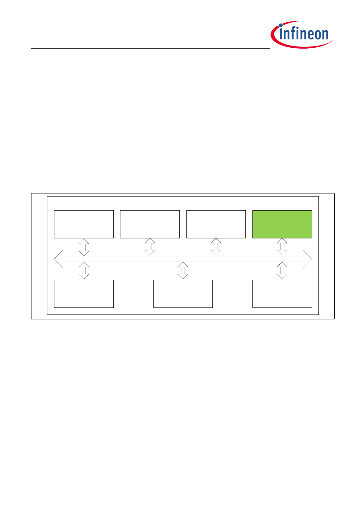
Figure 2-1 shows the TLE984x components used during execution of the BootROM.
, and so represents the standard reset handler
H
Figure 2-1 Block Diagram of the BootROM and its Interaction with other TLE984x Components
The startup procedure is the first software-controlled operation in the BootROM that is automatically
executed after every reset. Certain startup submodules are skipped depending on the type of reset (more
details are provided in “Reset Types” on Page 14) and the error which might occur (more details are provided
in “Startup Error Handling” on Page 17).
The startup procedure includes the NVM initialisation, PLL configuration, enabling of NVM protection,
branching to the different modes and other startup procedure steps.
There are two (2) operation modes in the BootROM :
•User/BSL mode
•Debug Support mode
The deciding factor will be on the latch values of TMS and P0.0 upon a reset. During reset, these signals are
latched at the rising edge of RESET pin. Details are provided in “Boot Modes” on Page 10.
Firmware User Manual (AE-step) 7 Revision 1.02
2019-04-24
Page 8

TLE984x Firmware User Manual
Overview
2.2 Program Structure
The different sections of the BootROM provide the following basic functionality.
Startup procedure
The startup procedure is the main control program in the BootROM. It is the first software-controlled
operation in the BootROM that is executed after any reset.
The startup procedure performs initialization steps and decode the pin-latched values of the TMS and P0.0 to
determine which mode to execute.
User mode
It is used to support user code execution in the NVM address space. However, if the NVM is not protected and
the Bytes at address 11000004
If a valid user reset vector was found at 11000004
and a proper NAC value is found then the BootROM proceeds into user mode.
In case an invalid No Activity Counter value is found (see also “NAC Definition” on Page 11), the device waits
indefinitely for a FastLIN BSL communication.
-11000007H are erased (FFH), then device enters sleep mode.
H
(values at 11000004H - 11000007H not equal to FFFFFFFFH)
H
LIN BSL mode
It is used to support BSL via LIN like protocol. Downloading of code/data to RAM and NVM related
programming is supported in this mode.
FastLIN BSL mode
It is used to support BSL via FastLIN protocol. Downloading of code/data to RAM and NVM is supported in this
mode.
2.3 RAM Structure for User
With user mode entry, the entire RAM is available to the user, but upon a reset the BootROM uses parts of the
RAM for variables and for its program stack. For a reset type with no RAMBIST execution (e.g. softreset), user
data outside the BootROM reserved RAM range will not get changed.
The BootROM RAM range is defined to go from 0x1800.0000 - 0x1800.03FF
Firmware User Manual (AE-step) 8 Revision 1.02
2019-04-24
Page 9
TLE984x Firmware User Manual
SWD Debug
Mode
STARTUP_ARCHITECTURE_UM
.
Libraries
(used by all
modules)
MBIST
NVM /
CS
NVM HALRAM
Timer
Watchdog
Clock / PLL
Analog Module
Trimming
Clock / PLL
HAL
Analog Module
HAL
BootROM Startup procedure
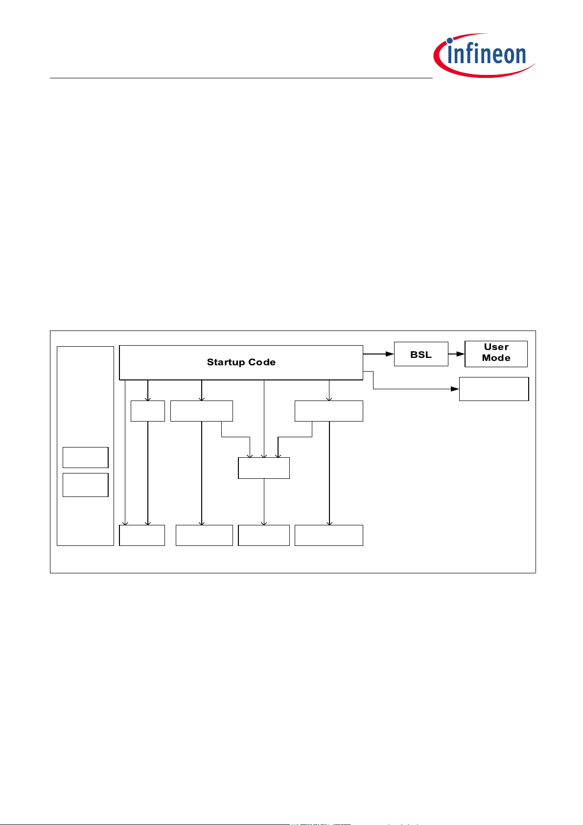
3 BootROM Startup procedure
This chapter describes the BootROM startup procedure in TLE984x.
The startup procedure is the first software-controlled operation in the BootROM that is automatically
executed after every reset.
There are 2 operation modes in the BootROM :
•User/BSL mode
•Debug Support mode
The operation modes get selected dependent on the latch values of two (2) pins upon reset. Details are
provided in “Boot Modes” on Page 10.
For each HW module a HW abstaction layer (HAL) is implemented with its associated module specific firmware
functions called by the BootROM startup procedure.
Figure 3-1gives an overview by showing the startup code partitioning into firmware modules and the
corresponding dataflow.
Figure 3-1 Startup Procedure Architecture Overview
The startup code performs different device initialization steps.
After initialization, the BootROM either starts BSL communication (according to configuration) or jumps to
user mode code execution.
For user mode, BootROM will execute the startup procedure, redirect the vector table to the beginning of the
NVM in user accessible space (by proper setting of the VTOR register) and jump to the customer defined reset
handler routine (jump to the address pointed by the address 11000004
) to execute the user program.
H
3.1 Startup Program Structure
The first task executed by the BootROM startup procedure is to check the reset type.
The BootROM also reads the logical state of certain external Pins (see “Boot Modes” on Page 10) to decide
which initialization sub modules to be executed or to be skipped during the startup sequence.
Firmware User Manual (AE-step) 9 Revision 1.02
2019-04-24
Page 10
TLE984x Firmware User Manual
BootROM Startup procedure
A list of supported boot mode pin selections is given in “Boot Modes” on Page 10.
Many of the called initialization parts require further configuration parameters which are stored in the NVM CS
(Configuration Sector).
The initialization process differs slightly between each selected boot mode. Each boot mode has a different
set of initialization steps to be performed. For instance, some initialization steps might be skipped for one
mode but carried out for another mode.
The functional blocks are listed in Table 3-1.
Table 3-1 Functional Blocks
Block Description Reference
Watchdog Disable The WDT1 is disabled, depending on the boot mode. Section 3.8.1
RAM MBIST Performs RAM MBIST (optional).
RAM Init Inits RAM to zero (mandatory).
MapRAM Init Inits MapRAM based on MapBlock data Section 5.3
Analog Module
Trimming
Analog module NVM CS trimming values are configured in the hardware. Section 3.8.3
Section 3.8.2
PLL Init Switch system clock to PLL Section 3.5
Start NAC Timer Start a timer which is dedicated to the user mode / BSL “no activity count
timeout” calculation.
BSL BSL communication Chapter 4
Section 3.8.5
3.2 Boot Modes
The different BootROM-supported boot modes are listed in Table 3-2 “BootROM Boot Modes” on Page 10.
These boot modes are pin-latched during reset release. The mode decides which initialization parts are to be
executed by BootROM.
Table 3-2 BootROM Boot Modes
TMS /
SWD_IO
0X USER_BSL_MODE User Mode / BSL Mode
11 SWD_DEBUG_MODE Debug Support Mode with SWD port
All other values Reserved for internal use
P0.0 /
SWD_CLK
Mode / Comment
3.3 Debug Support Mode entry (with SWD port)
Debug support mode is available for SWD. The BootROM starts the overall device initialization as described in
“Startup Program Structure” on Page 9.
The BootROM then enters a waiting loop to synchronize with the debugger connected to the Serial Wire Debug
(SWD) interface. After that, the BootROM finishes the boot process and starts to execute user code under
control of the debugger.
Firmware ensures that jumping to user code in user mode entry or customer debug entry is performed with
identical RAM and SFR content, except WDT1.
Firmware User Manual (AE-step) 10 Revision 1.02
2019-04-24
Page 11

TLE984x Firmware User Manual
BootROM Startup procedure
The watchdog is always disabled in debug support mode, except when the debug error loop is entered after a
boot error.
3.4 NAC Definition
The No Activity Counter (NAC) value defines the time window after reset release within the firmware is able to
receive BSL connection messages. If no BSL messages are received on the selected BSL interface during the
NAC window and NAC time has expired the firmware code proceeds to user mode.
NAC is a byte value which describes the timeout delay with a granularity of 5 ms. The NAC timeout supports a
maximum of 140 ms.
For example:
•NAC=05
•NAC=16
After ending the start up procedure, the program will detect any activity on the LIN/ FastLIN interface for the
remaining NAC window. When noactivity is detected, the program will jump to user mode. To determine the
minimum required NAC value, the baudrate, the interframe gap and the BSL passphrase requirements need
to be taken into account. For more details, refer to “LIN / FastLIN Passphrase” on Page 20
In case a valid BSL passphrase is detected during the BSL window the firmware suspends the counting of the
WDT1 in order to avoid that requested BSL communication is broken by a WDT1 reset. The firmware will then
re-enable WDT1 before jumping to user code.
indicates a timeout delay of 25 ms (5D x 5 ms) before jumping to user mode
H
indicates a timeout delay of 110 ms (22D x 5 ms) before jumping to user mode
H
If NAC is 00
, the BSL window is closed, no BSL connection is possible and the user mode is entered without
H
delay.
If NAC is FF
, no timeout is used, BootROM code will switch off WDT1 and wait indefinitely for a BSLconnection
H
attempt.
3.5 User and BSL Mode Entry (UM)
Entry to user mode is determined by the No Activity Count (NAC) value,see “NAC Definition” on Page 11.
After waiting the time defined by the current NAC value, the startup procedure sets the VTOR register to point
to the beginning of the NVM (11000000
) and jumps to the reset handler. If a NVM double Bit error occurs when
H
reading the NAC value, the system goes into an endless loop waiting for BSL communication. Before entering
User mode (except for Hot Reset, see Figure 3-2 “Flowchart – Start BootROM” on Page 13), the system clock
frequency is switched to PLL output and to the max. frequency as stated in the datasheet. In case PLL has not
locked within 1 ms, the clock source fINTOSC/4 (20 MHz) will be used.
User mode is entered by jumping to the reset handler. This can happen directly from startup routine, after a
waiting time for possible BSL communication, or as a result of BSL commands. In all these cases, a jump to
user mode will only occur if the NVM content at 11000004
-11000007H is not FFFFFFFFH. Otherwise, the
H
BootROM executes an endless loop.
3.5.1 Unlock BSL Communications
The BootROM locks the BSL LIN and FastLIN communication after reset to avoid unexpected BSL
communication on the customer side. The host needs to unlock the communication by sending a passphrase
sequence to the BootROM.
Details about this passphrase and how it influences the NAC timeout are given in “LIN / FastLIN Passphrase”
on Page 20.
Firmware User Manual (AE-step) 11 Revision 1.02
2019-04-24
Page 12

TLE984x Firmware User Manual
BootROM Startup procedure
3.5.2 Post User Mode Entry Recommendations
Upon USER MODE entry, it is highly recommended to to perform the following checks and actions:
Prior to any NVM operation, it is recommended to implement a test of SYS_STRTUP_STS.Bit1.
If the bit is clear then the data flash mapping is consistent NVM write/erase operation can be performed. To
see if the Service Algorithm might have been active the user has to check the MEMSTAT register. If the Service
Algorithm was active the user has to expect that expected logical data flash pages are not present anymore.
The user has to take care of this and reconstruct any missing page. Furthermore it might be possible that the
Service Algorithm reports an unrecoverable failure inside the Data Flash, then the same corrective actions
shall be applied as described in the following paragraph for the case that SYS_STRTUP_STS.Bit1 is set.
If the SYS_STRTUP_STS.Bit1 is set, then the data flash mapping is inconsistent, the mapping might not be
complete and any NVM operation like write or erase is not safe and might cause further inconsistencies inside
the data flash. As corrective actions the user might reset the device (cold reset) in order to give the Service
Algorithm a chance to repair the data flash sector. If this attempt fails again, then a sector erase is needed to
reinitialize the data flash sector and to remove any mapping inconsistency. After the data flash sector has
been erased the user has to take care of reconstructing the expected logical data flash pages.
The reset source should get read from the PMU Reset Status Register (PMU_RESET_STS). Clearing
PMU_RESET_STS is strongly recommended in the user startup code, as uncleared bits can cause a wrong reset
source interpretation in the BootROM firmware after the next reset (e.g. handling a warm reset as a cold reset)
The system startup status register SCU.SYS_STRTUP_STS should get checked for any startup fails. The bit
INIT_FAIL which is a logical or of all modul status bits should get checked at least. See the TLE984xQX User’s
Manual for a detailed register description
3.6 Flowcharts for User BSL / Debug Modes
This section provides the firmware flow charts that are relevant for user and debug boot modes.
Firmware User Manual (AE-step) 12 Revision 1.02
2019-04-24
Page 13
TLE984x Firmware User Manual
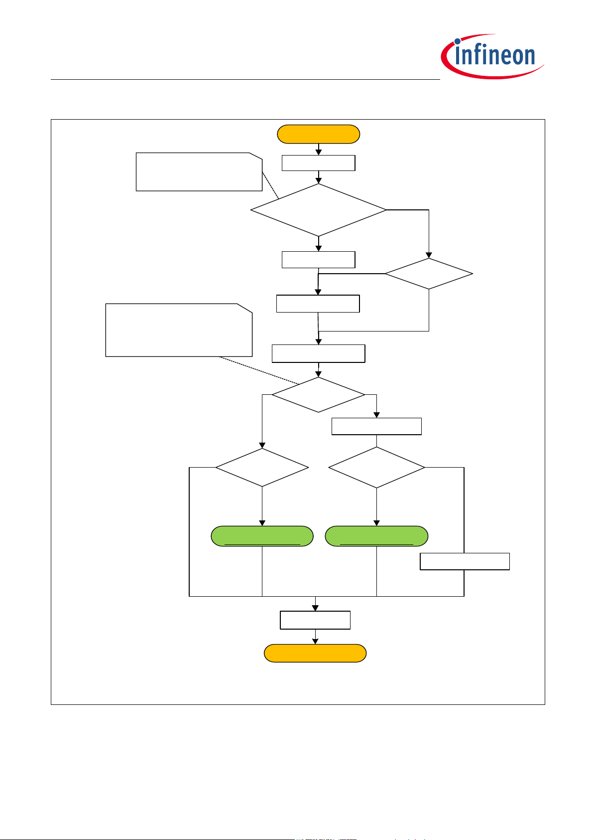
STARTUP_FLOW_RESET_UM
Boot mode
select
Start
Start Timer
Cold_ Reset
OR
NVM_CS bit0 = 1
RAM MBIST
Disable W atchdo g
Ena ble debug loop
Clear Timer
Clear RAM
Warm_Rese t?
RAM test OK? RAM test OK?
Loop forev er
SWD De bu g mod e
User BSL mode
Yes
No
No
Yes
Yes
No
No
Yes
user_mode_entry
(debug = Disabled)
user_mode_entry
(debug = Enabled)
NVM_CS is
CS_NVM_RAM_MBIST
Boot mode selection is done via
TMS and P 0.0 pins :
1) 0X = USER_BSL_MODE
2) 11 = SWD_DEBUG_MODE
Ena ble Watc hdog
BootROM Startup procedure
Figure 3-2 Flowchart – Start BootROM
Firmware User Manual (AE-step) 13 Revision 1.02
2019-04-24
Page 14
TLE984x Firmware User Manual
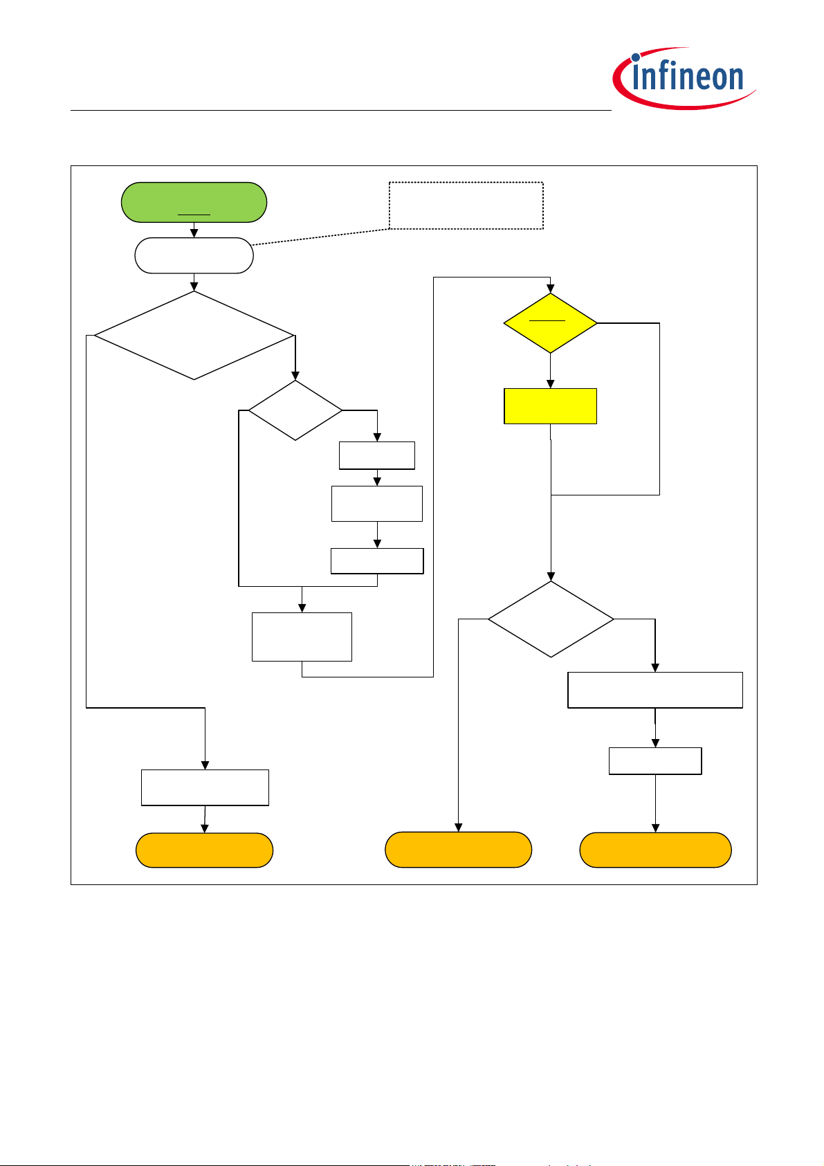
user_mode_entry
(debug)
Hot_Reset?
BSL
Use r mode error
handling
(NVM init)
OR (NVM Pr otection)
OR (Analog module Trimm)
Error?
Clk to PLL
switch
Clear inter rupts
Time r, UART, LIN
registers reset
debug =
Enabled?
Wait for
debugger
Clear RAM
Use r code addr.
is Valid?
Re-map vector table to NVM
Loop forever
(unprotected code area)
Jump to user code
NoYes
Yes
No
Yes
No
Dev ice conf igur ation
prep ar e
Loop forever
(protec ted cod e area)
Yes
No
Init N VM
Apply NVM Protection
Analog module Trim
BootROM Startup procedure
Figure 3-3 Flowchart – User BSL Mode
3.7 Reset Types
The BootROM classifies the different hardware resets according to the following reset types:
•Cold reset
•Warm reset
•Hot reset
Firmware User Manual (AE-step) 14 Revision 1.02
2019-04-24
Page 15

TLE984x Firmware User Manual
BootROM Startup procedure
Cold reset
The reset events generated from the following sources, are classified as cold resets :
• POR : Power-on reset
•Pin reset
• Watchdog reset
•System fail
After a cold reset, all initialization steps, listed in Table 3-1 “Functional Blocks” on Page 10, are processed
in accordance with the boot mode.
Warm Reset
The reset events generated from the following sources, are classified as Warm resets :
• Sleep-exit reset
•Stop-exit reset
After a warm reset, the following initialization steps, listed in Table 3-1, are processed, except :
• RAM memory test - MBIST - (only executed if forced by NVM CS configuration, as described in “RAM Test
(MBIST) and RAM Initialization” on Page 16)
Hot Reset
The reset events generated from the following sources, are classified as Hot resets :
• Software triggered reset
• Lock-up reset
After a Hot reset, the following initialization steps, listed in Table 3-1, are processed, except :
• RAM memory test - MBIST - (only executed if forced by NVM CS configuration, as described in “RAM Test
(MBIST) and RAM Initialization” on Page 16)
• Download of analog module trimming parameters (incl. oscillator and PLL settings)
• Switch system clock to PLL output
Reset priority
In case more than one reset event occur, the post reset initialization procedure with the highest priority type
is executed. The priority is evaluated according to this priority order (where “1” is the highest priority):
1. Cold reset
2. Warm reset
3. Hot reset
Attention: The reset source is read from the PMU Reset Status Register (PMU_RESET_STS). Clearing
PMU_RESET_STS is strongly recommended in the user startup code, as uncleared bits can
cause a wrong reset source interpretation in the BootROM firmware after the next reset (e.g.
handling a warm reset as a cold reset).
See also “Post User Mode Entry Recommendations” on Page 12.
3.8 Startup Procedure Submodules
The following submodules are described in this section.
• Watchdog configuration
Firmware User Manual (AE-step) 15 Revision 1.02
2019-04-24
Page 16

TLE984x Firmware User Manual
BootROM Startup procedure
• RAM Test (MBIST) and RAM initialization
• Analog module trimming
• Startup Error Handling
• No Activity Counter (NAC) Configuration
• Node Address for Diagnostics (NAD) Configuration
3.8.1 Watchdog Configuration
After a reset, the watchdog WDT1starts with a long open window. For all the reset types, firmware startup in
user mode enables WDT1 before jumping to user code, and the watchdog cannot be disabled while user code
is being executed.
The watchdog WDT1is disabled before entering into debug mode. WDT1 continues running while waiting for
the first BSL frame. If host synchronisation is completed during the BSL waiting time (defined by NAC), WDT1
is disabled and its status is frozen.
WDT1 continues running while waiting for the first BSL frame. If host synchronisation is completed during the
BSL waiting time (defined by NAC), WDT1 is disabled and its status is frozen.
3.8.2 RAM Test (MBIST) and RAM Initialization
The RAM memory test is performed for cold reset type.
The RAM initialization is performed for cold and warm reset types.
It is possible to force a RAM test and the RAM initialization for the whole RAM range during startup regardless
of reset type. This can be done by enabling the feature using the user API function “user_mbist_set” on
Page 81. Exception for the forced test is that for WARM reset the first 1kB of the RAM will not be checked.
User_ram_mbist() must therefore be called by the user on the first 1kB RAM range to make sure RAM test and
RAM initialization is performed and no errors exist (user_ram_mbist(0x18000000, 0x180003FF) ).
When executed, the RAM MBIST test destroys the contents of the tested RAM. It consists of a linear write/read
algorithm using alternating data. RAM MBIST execution is user configurable for all reset types, see
“user_mbist_set” on Page 81.
Prior to calling MBIST to test the first 1kB of RAM, stack and variables must be moved to the already tested RAM
range above 1kB.
In case an error is detected in the RAM MBIST, the appropriate error status is captured and the device enters
an endless loop. As the watchdog is enabled when entering the endless error loop after a boot in user or
debugmode, a WDT1 cold reset is asserted after timeout and the RAM test is re-executed.
After five (5) consecutive watchdog resets, the device enters SLEEP mode (by hardware function).
The RAM initialization writes the whole RAM to zero with the proper ECC status. This is needed to prevent an
ECC error during user code execution due to a write operation to a non initialized location (with invalid ECC
code).
Note: The standard RAM interface is disabled during MBIST test execution.
Firmware User Manual (AE-step) 16 Revision 1.02
2019-04-24
Page 17

TLE984x Firmware User Manual
BootROM Startup procedure
3.8.3 Analog Module Trimming
During analog module trimming, the trimming values of PMU, voltage regulators, LIN module, temperature
sensor, oscillator, PLLand other analog modules are read from the NVM configuration sector and written into
the respective SFR registers. In case 100TP pages with data for the trimming process contains CRC errors, the
predefined ones are used.
• 100 Time Programmable data (user data)
– User has eight 100 time programmable pages. The values of the first (page 0) and second (page 1) pages
are automatically copied into the dedicated SFR registers after every COLD or WARM reset thus
replacing the registers default reset values. The user can check them by reading the dedicated SFRs or
by reading directly the content of the page.
– This procedure allows the user to configure the ADC1 . The complete list of SFR registers is provided in
“Appendix D – Analog Module Trimming (100TP Pages)” on Page 110
– In case the first and second 100TP NVM CS (Configuration Sector) pages do not contain valid trimming
data (CRC failure), the BootROM reports error and downloads alternative backup trimming values.
For BootROM reported error handling see “Post User Mode Entry Recommendations” on Page 12.
3.8.4 Startup Error Handling
To ensure that the device is properly booted, error checking and error handling are added to the startup
procedure
For USER_BSL_MODE, the overall startup sequence ends up in an endless loop or SLEEP mode in the event
that any called submodule returns an error.
If a startup error occurs – except for double-bit errors for NVM reading – and the boot option is
USER_BSL_MODE, the device is set to a safe mode with limited access to HW resources. If the errors persist
after five (5) WDT1 triggered timeouts, the device enters SLEEP mode.
Regardless of the boot mode, the system enters an endless loop in the case of NVM double-bit errors when
reading the NVM contents.
For BootROM reported error handling see “Post User Mode Entry Recommendations” on Page 12.
Note: MON inputs must not be floating in order to prevent an unintended wakeup.
3.8.5 No Activity Counter (NAC) Configuration
A NAC timeout value is stored in the NVM CS. It is stored as a value and bit-inverted value in a dedicated
NVM CS page.
During user mode, this parameter is read from the NVM CS (Configuration Sector) and verified against the
stored inverted value. This parameter is provided as an API parameter when calling the BSL module. For
details, refer to Section 3.4.
If the NVM CS does not contain a valid NAC, a “wait forever” NAC (NAC=FF
The BootROM offers 2 user API functions to read and write NAC parameter:
• user_nac_get
) is given to the BSL module .
H
• user_nac_set
Firmware User Manual (AE-step) 17 Revision 1.02
2019-04-24
Page 18

TLE984x Firmware User Manual
BootROM Startup procedure
3.8.6 LIN Node Address for Diagnostics (NAD) Configuration
For LIN, a NAD is stored in the NVM CS (Configuration Sector). It is stored as a value and bit-inverted value in a
dedicated NVM CS (Configuration Sector) page.
During user mode, this parameter is read from the NVM CS (Configuration Sector) and verified against the
stored inverted value. The parameter is provided as an API parameter when calling the LIN BSL module. For
details, please refer to “Node Address for Diagnostic (NAD)” on Page 33.
If the NVM CS (Configuration Sector) does not contain a valid NAD, a “broadcast” NAD (NAD=FF
LIN BSL module .
The BootROM offers user APIs for reading and writing NAD parameter:
• user_nad_get
• user_nad_set
) is given to the
H
Firmware User Manual (AE-step) 18 Revision 1.02
2019-04-24
Page 19
TLE984x Firmware User Manual
BSL Protocol
BSL
FAST-LIN
Protocol
UART
HAL/Drv
Libraries
(used by all
modules)
Timer
NVM /
CS
NVM
HAL
LIN
Prot oco l
LIN
HAL/Drv
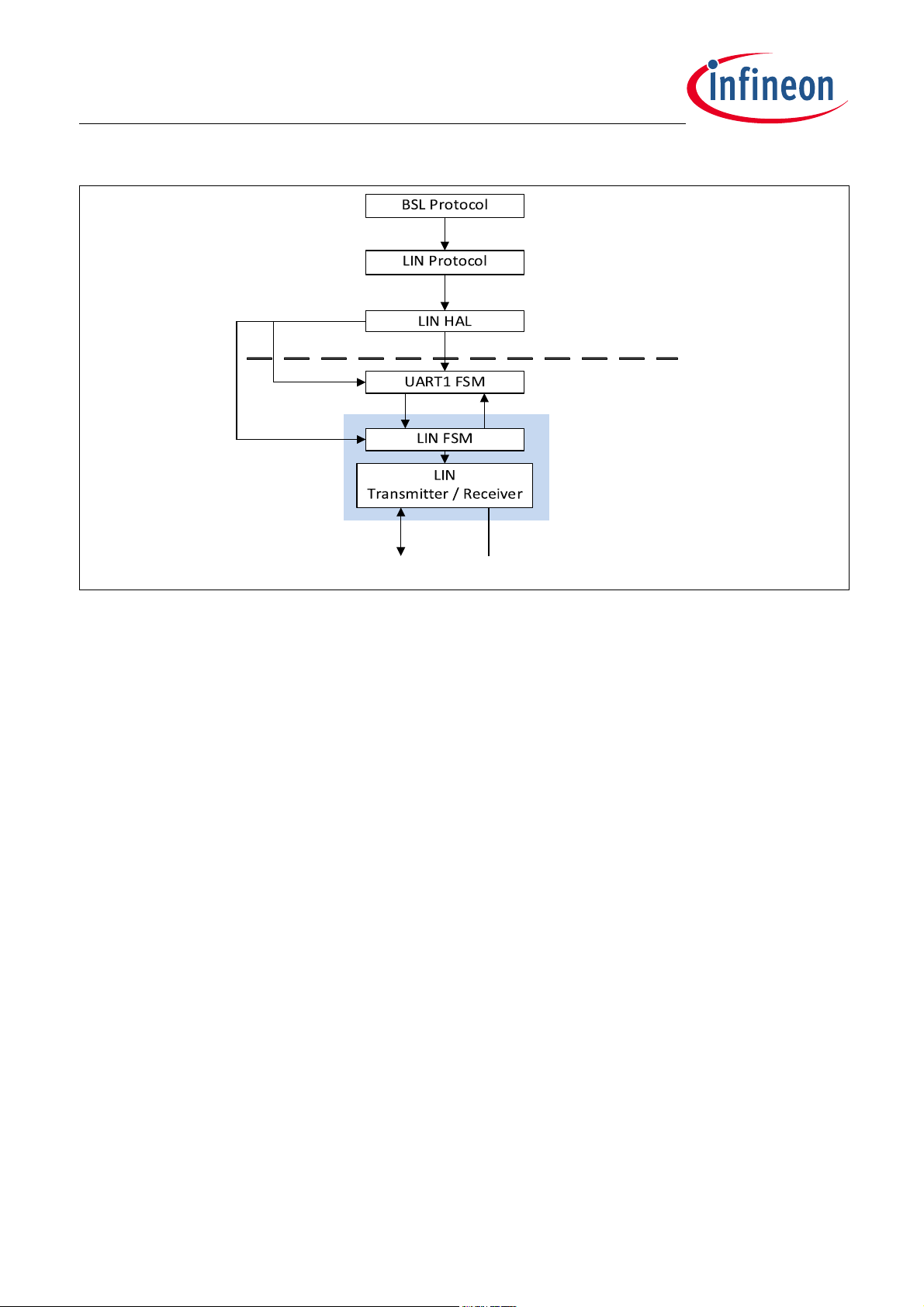
Boot Strap Loader (BSL)
4 Boot Strap Loader (BSL)
The BSL (Boot Strap Loader) module supports handling of message-based command request and response
communication over the serial LIN interface. The received command messages are parsed and executed
according to the LIN or FastLIN protocol. Details about this message protocol are given in “BSL commands -
Protocol (Version 2.0)” on Page 38.
The device supports the following serial interfaces :
- LIN
- Fast-LIN (LIN interface using the UART protocol)
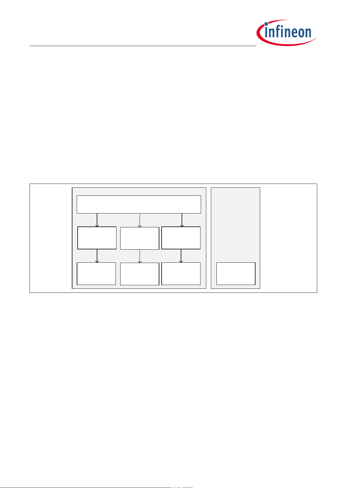
Figure 4-1 shows the various software submodules in the BSL module. The shared protocol is handled on a
single protocol level that processes all messages described in “BSL commands - Protocol (Version 2.0)” on
Page 38.
Figure 4-1 BSL Architecture
All command messages are encapsulated in an interface-specific frame format. This format includes specified
parameters, such as a checksum calculation and overall message size. Also specified on this level is whether
the interface is used as a peer-to-peer connection or as a master-slave-bus communication, which includes
device node addressing. This interface-specific frame handling is implemented in the interface-specific
protocol layer (e.g. LIN protocol).
The BSL protocol layer performs the command execution based on the parsed BSL commands. This results in
programming of the NVM, NVM CS (Configuration Sector), downloading to RAM or execution of NVM/RAM
code. It also includes the aspect that some commands are blocked based on applied hardware protection or
boot mode selection.
4.1 BSL overview
In this chapter, more details about the BSL mechanisms are provided.
Firmware User Manual (AE-step) 19 Revision 1.02
2019-04-24
Page 20

TLE984x Firmware User Manual
Boot Strap Loader (BSL)
4.1.1 BSL Selector
The BootROM supports specification of a BSL interface selector in the NVM CS for user-/debug mode. This
selector parameter is read and verified by the startup routine and provided as an API call parameter to the
software module.
This interface selector can be read with the user API routine user_bsl_config_get, and can be modified with
the routine user_bsl_config_set.
4.1.2 BSL Interframe Timeout
The interframe timeout is a configuration parameter read by BootROM startup code from the NVM CS
(Configuration Sector).
Interframe timeout parameter has the same format as NAC value (1 = 1x5ms, 2 = 2x5ms ...).
The paramter value is set to 0x38, which results in a timeout value of 280ms (0x38 x 5ms).
4.1.3 NVM / RAM Range Access
Some BSL commands allow access to the NVM and some to the RAM. In BSL mode the following memory
ranges are accessible for read and write operations:
• All user accessible NVM and NVM CS pages.
• The 100TP pages
• The RAM area , apart from the BootROM global variables and stack (648 bytes from 18000178H to
180003FFH).
4.1.4 LIN / FastLIN Passphrase
The BootROM locks the BSL LIN and FastLIN communication after reset to avoid unexpected BSL
communication on the customer side. The host needs to unlock the communication by sending a passphrase
sequence to the BootROM.
A passphrase consists of two (2) consecutive frames, where each frame contains a set pattern. To unlock the
BSL communication, both passphrase frames have to be sent by the host. Any other received message within
the passphrase sequence stops the unlock sequence. The unlock procedure always restarts on receiving the
first passphrase frame.
The contents of both passphrase frames are described in Figure 4-2.
Firmware User Manual (AE-step) 20 Revision 1.02
2019-04-24
Page 21

TLE984x Firmware User Manual
BSL20_ PASSPHRASE
.
0
0x46
‚F‘
1
0x4C
‚L‘
2
3 4 5 6
0x49
‚I‘
0x4E
‚N‘
0x50
‚P‘
0x41
‚A‘
0x53
‚S‘
Passphrase Frame #1:
0
0x53
‚S‘
1
0x50
‚P‘
2
3 4 5 6
0x48
‚H‘
0x52
‚R‘
0x41
‚A‘
0x53
‚S‘
0x45
‚E‘
Passphrase Frame #2:
Boot Strap Loader (BSL)
Figure 4-2 Passphrase Content
For LIN communication, the passphrase frames are encapsulated by sync break, sync char, protected ID, NAD
and checksum byte fields. A passphrase frame is rejected in case of incorrect received NAD or checksum bytes.
For FastLIN communication, the frames are extended by the checksum byte. Details about the encapsulation
are given in Section 4.2.
The BootROM ignores and rejects all received LIN and FastLIN frames if the communication is still locked. This
rejection includes frames with valid NAD and checksum fields. It does not reply to any received passphrase
frames.
The NAC timeout stops when the communication is unlocked after receiving the second valid passphrase
frame. For more details about NAC timout, refer to Section 3.4.
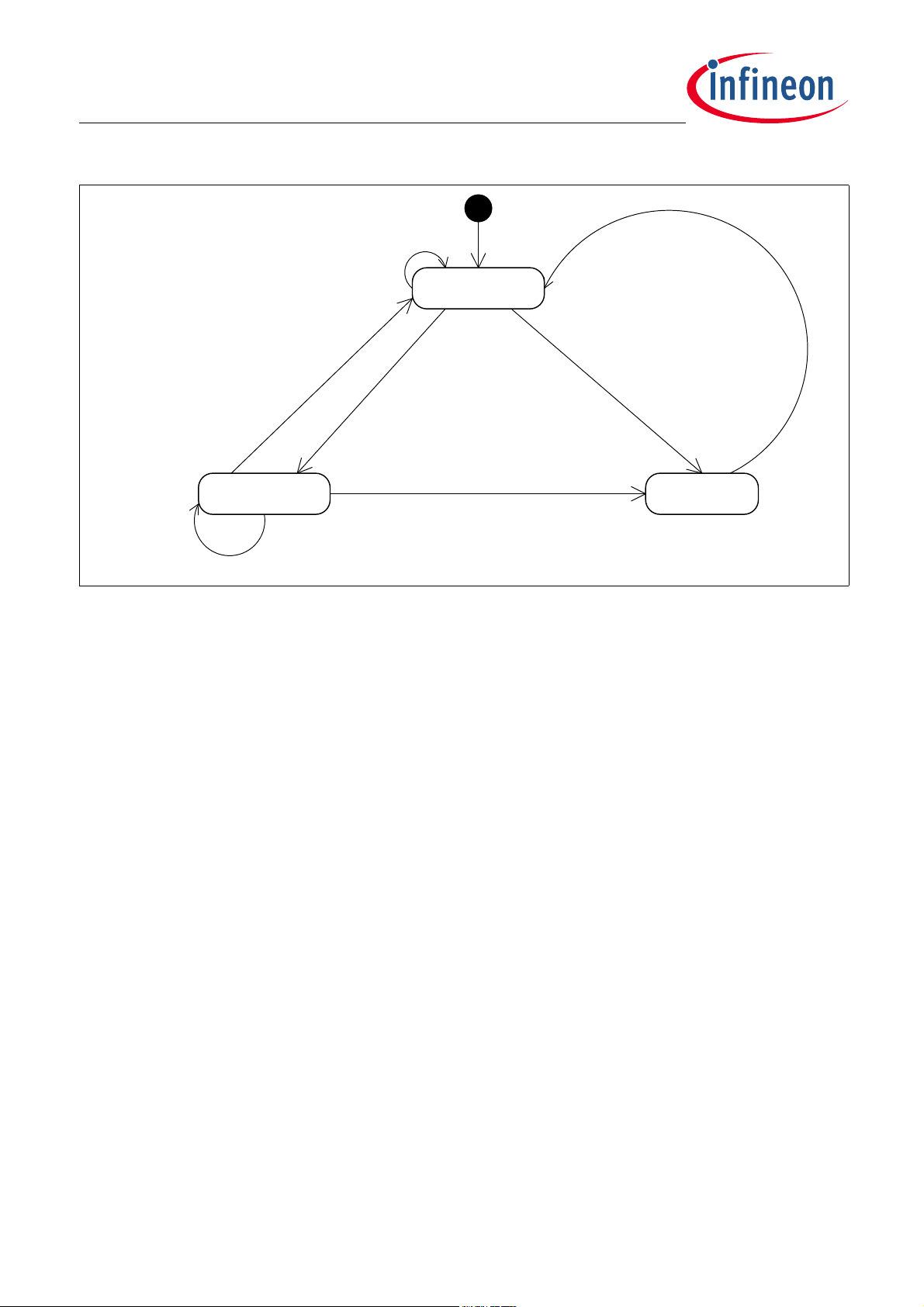
4.1.5 BSL Message Parsing & Responses
The BSL protocol provides single message commands and multimessage commands. A message state
machine is implemented, which first collects all command-related messages before executing the command.
It periodically polls the underlying interface protocol layer (e.g. LIN protocol layer) to collect all frames
belonging to a BSL command.
Command Message State Machine
Figure 4-3 gives an overview of the BSL command message state machine.
Firmware User Manual (AE-step) 21 Revision 1.02
2019-04-24
Page 22
TLE984x Firmware User Manual
BSL_MSG_PARSE _STAT ES
.
Po lling N ew Messag es
(Non Data or EOT Block ) ||
(length > message length)
Data Block
EOT Block
Command
processed
Multi
Message
Command
Single
Message
Command
Multi Message Collec t Command Process
Non Header
Block
Boot Strap Loader (BSL)
Figure 4-3 BSL Command Message State Machine
The state machine starts to wait for the header block. This could be either a command which consists of a
single header block (the message type MSB bit is set) or a command that consists of multiple messages (the
message type MSB bit is zero).
For multimessage commands, all message data is collected by receiving data block messages. The last
message data is always received by an EOT block message.
The EOT block message reception initiates command parsing and execution.
The command processing includes message validation, where the message parameters are checked for
boundaries, any hardware applied protection and if this message is supported for this boot mode.
The state machine aborts the multimessage collection if the overall data bytes of all collected messages have
exceeded the maximum message data buffer length of 137 bytes (7 bytes in the header block message +
130 EOT data bytes).
For single message commands, all command-related information is already available in the header block
message. The command parsing and execution start right after receiving the message.
After command execution and after a response has been sent, the state machine returns to the header block
polling state in order to wait for the next command.
Any received message which does not fit the current state or state transmission leads to an exit from the
current state and restarting of the whole state machine.
Response Message State Machine
The command response is specific to the used serial interface. For instance, LIN slave devices only send out
response frames if a slave response header was received from the LIN bus master. Further details are
described in the interface specific protocol layer part.
Figure 4-4 gives an overview of the LIN response message state machine.
Firmware User Manual (AE-step) 22 Revision 1.02
2019-04-24
Page 23

TLE984x Firmware User Manual
BSL_MSG_R ESPONSE _PAR SE _STATES
.
(Multi Msg Command &
Error occurred) ||
(Single Msg)
Multi msg command &
No error occurred
Response data left
greater than
EOT msg size
Response data left
not gr e ate r than
EOT msg size
Send Data Msg
Send EOT Msg
Send Response
Msg
Result ResponseEOT MsgData Msg
Command ProcessedData Response
Boot Strap Loader (BSL)
Figure 4-4 LIN Response Message State Machine
Some BSL messages request read-out of data from the device. These messages expect multimessage
responses. The responses are sent out using data block and EOT block messages, where the data block
messages are only used for the data that does not fit in the EOT block message. The EOT block message is the
last message for such responses.
Other BSL messages download data or initiate code execution. They do not request reading out of any data.
These messages only reply with a status response message.
A BSL command execution replies with a status response message in the event that the command execution
fails.
Attention: The BootROM responds to each incoming command. This is either the requested data or the
response block (e.g. success or error code). Only the code execution command does not reply
with a response message.
Firmware User Manual (AE-step) 23 Revision 1.02
2019-04-24
Page 24

TLE984x Firmware User Manual
Boot Strap Loader (BSL)
4.1.6 Command Execution
The command data is checked and validated after all the message data is received. This includes that the
message parameters are checked for boundaries, any hardware-applied protection (e.g. NVM protection) and
if this message is supported for this boot mode.
The following command classes are supported:
• RAM access – RAM accesses are directly done by the BSL protocol without the use of any other submodule.
• NVM access – NVM accesses (read/write) are performed using the NVM API.
• 100TP access – 100TP accesses are performed using the NVM CS (Configuration Sector) API.
• NVM CS (Configuration Sector) access – NVM CS (Configuration Sector) accesses are performed using the
NVM CS (Configuration Sector) API.
4.1.7 Timing Constraints
The host needs to add a delay between all sent BSL command header and EOT messages. Same delay must
be add between EOT and DATA block messages.
The BootROM also requires an additional waiting time to process the full received BSL command. The
BootROM is not able to provide the response messages or able to receive new commands before this period
expires. The host must wait this length of time before sending a new command or requesting the command
response (e.g. by sending a LIN slave response header).
To give BootROM time to process each byte and CMD/DATA/EOT frame, byte and frame timing must comply to
the values shown in Table 4-1.
Table 4-1 BSL Byte and Frame Timing Limits and Highest Transfer Rate
Delay type LIN (min.) FastLIN (min.)
Between bytes 4.1 µs 3.7 µs
Between end of CMD to
start of DATA or EOT frame
Interframe Timeout 280 ms 280 ms
Host waiting time for
message processing before
asking for response
Host waiting time after
response is received until a
new frame can be sent
* There are certain BSL commands that need longer processing time. These involve NVM write/erase
operations. The host waiting time is longer before a command response can be requested or before a result is
sent back. Changing a value in an already programmed NVM page, which happen if a setting is changed,
requires the following NVM steps:
- Read the full page into the HW buffer
- Update the HW buffer with new data
- Program the page from the HW buffer
20 µs 20 µs
100 µs * n/a
20 µs 20 µs
- Erase the old page
Firmware User Manual (AE-step) 24 Revision 1.02
2019-04-24
Page 25

TLE984x Firmware User Manual
Boot Strap Loader (BSL)
Total time: 8 ms
The processing time must always be taken into account.
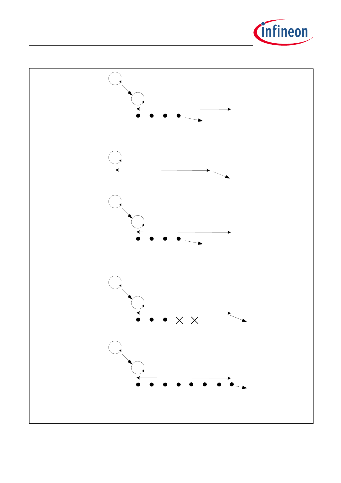
4.1.8 BSL Interframe timeout behavior
To keep track of BSL frame transmission violations, interframe timeout is used (described also in
Chapter 4.1.2). This chapter summarizes the different use-case scenarions where BSL frame timeouts are
applied.
BSL frame transmission timeout is handled differently and depends on:
• BSL has not received any valid host synchronization yet. In this case NAC timeout value is used for all
timeout calculations. If timeout is reached this means NAC timer expired.
• BSL has completed host synchronization. All timeouts are based on interframe timeout value. This means
wait forever for frame start and once frame reception has started, time measurement against interframe
timeout are performed.
Once host synchronization is done there are different scenarios how timeout is used.
More details are provided in Figure 4-5 related LIN communication (same concept for FastLIN) .
Note: When a LIN frame is received, its PID and NAD numbers are checked. If one of them doesn’t match, the
current frame is discarded and frame reception process is restarted with detection of break/sync
sequence.
Note: Valid host synchronization: For FLIN/LIN the full passphrase has been received before NAC expires.
Firmware User Manual (AE-step) 25 Revision 1.02
2019-04-24
Page 26
TLE984x Firmware User Manual
BSL20_LIN _IN TER FR AME_ BEHAVIOR
.
Get frame bytes
Start fra me time me asurement
Poll break/sync detection
Interframe
timeout
Status: Valid frame received
within timeout period
Received bytes
Normal frame
reception:
Interframe
timeout
Status : Timeout =>
restart break/sync
detection
No break/sync
detected:
Status: Valid frame received but
invalid length => wait interframe
timeout , then restart break /sync
detection
Invalid length :
Get frame bytes
Start fra me time me asurement
Interframe
timeout
Received bytes
Host stops
transmitting
data:
Get frame bytes
Start fra me time me asurement
Interframe
timeout
Received bytes
Frame receive
time violation :
Status: Frame receive
timeout => wait
interframe timeout ,
then restart break /
sync detection
Get frame bytes
Start fra me time me asurement
Interframe
timeout
Received bytes
Poll break/sync detection
Poll break/sync detection
Status: Timeout =>
restart break/sync
detection
Poll break/sync detection
Poll break/sync detection
Boot Strap Loader (BSL)
Figure 4-5 Handling of LIN frame timeouts
Firmware User Manual (AE-step) 26 Revision 1.02
2019-04-24
Page 27

TLE984x Firmware User Manual
LIN_PROT OCOL_LAYER
.
BSL
Protocol
LIN
Protocol
LIN
HAL
Timer
4.2 BSL via LIN
The LIN BSL is a LIN-like protocol based on LIN 2.0 (refer to LIN Specification Package documentation,
Revision 2.0, 23 September 2003).
The LIN protocol layer module handles incoming LIN frames. It forwards the given commands and requests to
the BSL protocol layer and is responsible for response message handling.
This layer calls the LIN HAL API to access the LIN hardware module for baud rate management and LIN frame
exchange (transmission & reception).
The LIN interface supports baud rate detection including the standard rates from 9.6 kbit/s to 57.6 kbit/s.
The LIN HAL is described in “LIN HAL” on Page 36.
The BSL software module periodically polls the LIN protocol layer to receive incoming frames and send out
available response frames.
The LIN protocol layer parses all incoming LIN frames, it rejects frames with wrong checksum calculation or
invalid NAD values. The checksum calculation algorithm is done according to the LIN 2.0 standard. All received
messages are given to the BSL protocol layer, which concatenates it to complete commands.
Some BSL commands are shorter than the expected LIN frame. Those frames are filled up with dummy bytes.
BootROM reads such dummy bytes during checksum validation, but it ignores them during command
processing. The dummy Bytes in both directions are always set to zero.
Figure 4-6 shows the LIN protocol layer and its interaction with other software modules.
Figure 4-6 LIN Protocol Layer
Figure 4-7 shows the interaction between Hardware and software layers for the BSL LIN mode .
Firmware User Manual (AE-step) 27 Revision 1.02
2019-04-24
Page 28
TLE984x Firmware User Manual
BSL_LIN_MODE_LAYERS
SW
HW
SFRs
Tx Rx
LIN GND_LIN
LIN Tranc ei ver
Figure 4-7 BSL LIN Mode HW/SW Layers
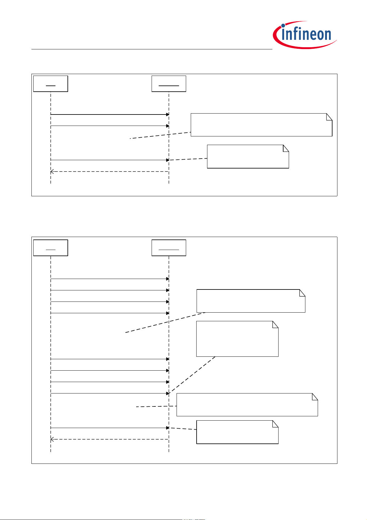
4.2.1 LIN frame format
For all supported modes, the command messages (see Command Message Protocol) are transmitted from
the host to the BootROM, requesting the commands to be executed. The response request messages (see
Response Message Protocol) are transmitted to check the status of the operation and to read out the data
requested (e.g. read RAM command).Upon a response request message, the requested data is sent from the
BootROM to the host.
Figure 4-8 shows the Master Request Header, Slave Response Header, Command and Response LIN frames.
The command and response LIN frames are identified as diagnostic LIN frames which have a standard 9-byte
structure.
Firmware User Manual (AE-step) 28 Revision 1.02
2019-04-24
Page 29

TLE984x Firmware User Manual
B12PHASEDETAIL
.
SYN
Break
(At least
13 bit low)
SYN
Char
55
H
Protected
ID
3C
H
Host BootROM
7 Data bytes for
Command
Checksum
(1 byte)
Master Request Header
Command
Slave Response Header
Checksum
(1 byt e)
Res ponse
SYN
Break
(At least
13 bit low)
SYN
Char
55
H
Protected
ID
7D
H
NAD
7 Data bytes for
Command
NAD
Figure 4-8 LIN mode - LIN Frames
The Master Request Header is transmitted from the host to the BootROM, followed by the command, which is
the header block. The Slave Response Header is transmitted to check the status of the operation. To save
protocol overhead, the BootROM supports multiple data block transfers, sending a Slave Response Header is
only allowed after the EOT block has been sent. Sending a Slave Response Header between data blocks will
result in a communication error. As the commands are sent one after another without waiting for any status
indication, a certain delay is required (as shown in Figure 4-9) to ensure sufficient time is provided for the
BootROM to execute the desired operations.
Figure 4-9 shows the LIN frame communication for BSL commands, where no data blocks and EOT blocks are
involved.
Firmware User Manual (AE-step) 29 Revision 1.02
2019-04-24
Page 30
TLE984x Firmware User Manual
LIN_FRAM E1_UML
Host BootROM
Master Request Header
Master Request Block (Command)
Sla ve Respo nse H eader
Slave Respons e Block
<<<< Delay >>>>
Slave Response communication
is not necessa ry and can
be skipped
Delay for processing and executing BSL command is needed.
Otherwise no response is possible
LIN_FRAM E2_UML
Host BootROM
Master Request Header
Master Request Block (Command)
Sla ve Respo nse H eader
Slave Respons e Block
Slave Response communication
is not necessary and can
be skipped
Delay for processing and executing BSL command is needed.
Otherwise no response is possible
Master Request Header
Master Request Block (Da ta)
<<<< Delay >>>>
Master Request Header
Master Request Block (Da ta)
…
…
…
...
Multiple Master Request Heade r and Blocks
are sent to download the all required data.
Master Request Header
Master Request Block (EOT)
Th e la st da ta ar e alwa ys se nt
with a EOT block frame.
This EOT triggers the BootROM
command processing
and execution.
Figure 4-9 LIN Communication: Command and Response
Figure 4-10 shows the LIN frame communication for BSL commands, where data are downloaded over data
blocks and EOT blocks.
Figure 4-10 LIN Communication: Data Command and Response
Firmware User Manual (AE-step) 30 Revision 1.02
2019-04-24
Page 31

TLE984x Firmware User Manual
LIN_FRAME3_ UML
.
Host BootROM
Master Request Header
Master Request Block (Command)
Delay for pr ocessing and ex ecutin g BSL comm and is need ed.
Otherwise no response is possible
Slave Response Header
<<<< Delay >>>>
Slave Response Header
…
…
…
...
Mult iple Slave Response Header are sen t by the Ho st ,
wh ere Boot ROM rep lies with Data Blo cks.
These Data Blocks c ontain t he req uired data.
BootROM sends the last
Bytes always with an EOT
packet.
Slave Response Block (D ata)
Slave Response Block (D ata)
Slave Response Header
Slave Response Bloc k (EOT )
MASTER_REQUEST _HEAD ER
.
Synch Char
(1 byte)
Synch Brea k
Protected ID
(1 byte)
Master Request Block
(9 byte)
Figure 4-11 shows the LIN frame communication for BSL commands, where data are read from the device.
BootROM provides such data over data blocks and EOT blocks.
Figure 4-11 LIN Communication: Request Command and Data Response
4.2.1.1 Command Message Protocol
This section describes the Master Request Header and the Master Request Block which are sent by the the
host for each LIN command frame. The Master Request Header contains synchronization bytes to detect the
start of a frame and to detect the baud rate.
Master Request Header
Table 4-2 Master Request Header Field Description
Field Description
Synch Break At least 13 bits must be low
Synch Char Always 55
Protected ID Always 3C
Master Request
Block
Firmware User Manual (AE-step) 31 Revision 1.02
2019-04-24
Commands as described in “Master Request Block” on Page 32.
H
H
Page 32

TLE984x Firmware User Manual
LIN_FRAME_FORMAT
.
Checksum
(1 byte)
BSL Protocol Block
(7 bytes)
NAD
(1 byte)
SLAVE_RESPONSE _HEAD ER
.
Synch Char
(1 byte)
Synch Break
Protected ID
(1 byte)
LIN_RESPONSE_FOR MAT
.
Checksum
(1 byte)
BSL Protocol Da ta/EOT/Response Block
(7 bytes)
NAD
(1 byte)
Master Request Block
A simple protocol is defined for the communication between the the host and BootROM. The Master Request
Header is followed by the Master Request Block.
Table 4-3 Master Request Block Field Description
Field Description
NAD Node Address for Diagnostic, specifies the address of the active slave node.
See Chapter 4.2.1.3.
BSL Protocol Block This field determines the type of the BSL message.
The size of this block is always 7 Bytes. The block is filled up with dummy Bytes (zeros) in
case the BSL message is smaller.
Checksum This checksum is calculated based on the NAD and BSL protocol block.
See Chapter 4.2.1.4.
4.2.1.2 Response Message Protocol
The BootROM reply is sent to the the host only when a Slave Response Header frame is received. The BootROM
reply is always sent in a transfer block of 9 bytes (consisting of Slave Response Header and Slave Response
Block).
Slave Response Header
This header is sent by the the host to initiate that the BootROM sends a Slave Response Block.
Table 4-4 Slave Response Header Field Description
Field Description
Synch Break At least 13 bits must be low
Synch Char Always 55
Protected ID Always 7D
H
H
Slave Response Block
Firmware User Manual (AE-step) 32 Revision 1.02
2019-04-24
Page 33

TLE984x Firmware User Manual
Table 4-5 Slave Response Block Field Description
Field Description
NAD Node address for diagnostics, specifies the address of the active slave node.
BSL Protocol
Data/EOT/Response
Block
This field determines the type of the BSL message.
Depending on the BSL command used, it could be either a data block, an EOT block or
a response block.
Checksum The checksum is calculated based on NAD, Response and Response Data bytes. All
responses sent by the BootROM adopts the classic checksum. See Section 4.2.1.4.
4.2.1.3 Node Address for Diagnostic (NAD)
This field specifies the address of the active slave node (only slave nodes have a NAD address). Each Master
Request Block contains a NAD field. Table 4-6 lists the BootROM-supported NAD address range.
The used NAD parameter is given as a BSL API parameter (for details see also “User and BSL Mode Entry
(UM)” on Page 11).
Table 4-6 NAD Address Range
NAD Value Description
00
80
FF
to 7F
H
to FF
H
H
H
H
Invalid slave address
Valid slave address
Broadcast address.
Default address (NAD value is invalid or it is not programmed)
Note: The LIN block with the standard LIN broadcast NAD (7F
) is ignored.
H
The firmware treats a received BSL message with NAD value of FFH as 'broadcast' message. BSL responds to
this no matter which NAD value is stored inside the NVM CS. A device with an invalid NAD value in NVM CS only
responds to a BSL 'broadcast' message.
4.2.1.4 Checksum
The checksum contains the inverted eight-bit sum with a carry over all data bytes. Data bytes are defined as
all bytes in the LIN frame excluding the protected ID byte.
Checksum calculation over the data bytes only is referred to as a classic checksum. An eight-bit sum with carry
is equivalent to the sum of all values, subtracted by 255 every time the sum is greater than or equal to 256.
Enhanced checksums are normally used for LIN 2.x devices, but frame identifiers (PID) 3C
classic checksum.
The checksum is the last field of Command and Response LIN frames.
always uses the
H
Firmware User Manual (AE-step) 33 Revision 1.02
2019-04-24
Page 34

TLE984x Firmware User Manual
LIN_FR AME_R AM_WRI TE_EXAM PLES
.
Write RAM Data
Host
BootROM
Master Request
Header &
Header Block:
EOT Block:
<<< Delay >= BSL command processing time >>>
*)
Length:
- 1-byte field
- Max. value: 129
D
- Min. value: 2
D
- Describ es the a mount of follo win g bytes in the frame.
Num:
- 1-byte field
- Number of data bytes the host wants to read or write
(exchanged by data & EOT block frames)
Data Byte s:
- Data bytes read or written
Address:
- 24-bit RAM offset to write data
Length*)0x 81
Response Block:
<<< Delay >= Message timing contrains µs >>>
Response Code
SYN 0x55 0x3C NAD Length*)0x02 Address
*)
Res Num*)CHKS
Data Block:
SYN 0x55 0x3C NAD Length*)0x00 Data Bytes
*)
CHKS
Data Block:
SYN 0x55 0x3C NAD Length*)0x00 Data Bytes
*)
CHKS
…
<<< Multiple Data Blocks >>>
...
SYN 0x55 0x3C NAD Length*)0x80 Data Bytes
*)
CHKS
Slave Response Header:
SYN 0x55 0x7D
NAD
CHKS
<<< Delay >= BSL frame processing time >>>
<<< Delay >= BSL frame processing time >>>
<<< Delay >= Message timing contrains µs >>>
4.2.2 LIN Message Examples
Figure 4-12 and Figure 4-13 provide some examples of how to write and read RAM using LIN BSL commands.
Figure 4-12 BSL RAM Write Access Frame Examples
Firmware User Manual (AE-step) 34 Revision 1.02
2019-04-24
Page 35

TLE984x Firmware User Manual
LIN_FR AME_R AM_R EAD_EXAM PLES
.
Read RAM Data
Host
BootROM
Master Request
Header &
Header Block:
EOT Block:
<<< Delay >= BSL command processing time >>>
*)
Length:
- 1-b yte field
- Max. value: 129
D
- Min. value: 1
D
- D escribes the amount of following b yte s in the frame.
Num:
- 1-b yte field
- Number of data bytes the host wants to read or write
(exchanged by data & EOT block frames)
Data Byte s:
- Data bytes read or written
Address:
- 2 4-bit R AM offset to rea d data
SYN 0x55 0x3C NAD Length*)0x84 Address
*)
Res Num*)CHKS
Data Block:
NAD Length*)0x00 Data Bytes
*)
CHKS
…
<<< Multiple Slave Response Header & Data Blocks >>>
...
NAD Length*)0x80 Data Bytes
*)
Slave Response Header:
SYN 0x55 0x7D
Data Block:
NAD Length*)0x00 Data Bytes
*)
CHKS
Slave Response Header:
SYN 0x55 0x7D
Slave Response Header:
SYN 0x55 0x7D
CHKS
<<< Delay >= Message timing contrains >>>
<<< Delay >= Message timing contrains >>>
<<< Delay >= Message timing contrains >>>
Figure 4-13 BSL RAM Read Access Frame Examples
Firmware User Manual (AE-step) 35 Revision 1.02
2019-04-24
Page 36

TLE984x Firmware User Manual
4.2.3 LIN HAL
The LIN HAL handles all SFR register accesses to the LIN hardware modules . These accesses include timing
critical register accesses and status polling mechanism.
Functionality
The following features are provided by the LIN HAL:
• BREAK condition detection on the LIN interface, used as indication for incoming packets.
• Baud rate detection
• Data reception
• Data transmission
LIN HW slope control is dependent on LIN or FastLIN mode selection:
For LIN fastslope is used.
For FastLIN flashmode slope is used.
The device requires some delay to process each received byte from header or EOT block or when transmitting
a response back.
Firmware User Manual (AE-step) 36 Revision 1.02
2019-04-24
Page 37

TLE984x Firmware User Manual
BSL_FAST_LIN_MODE_LAYER
S
SW
HW
SFRs
Tx Rx
LIN GND_LIN
LIN Tranc ei ver
4.3 BSL via FastLIN
FastLIN is a LIN enhancement supporting higher baud rates of up to 230.4 kBd. This rate is higher than the
standard LIN. FastLIN is especially useful during back-end programming, where faster programming time is
desirable.
The FastLIN BSL protocol supports baud rates of 38.4 kBd, 115.2 kBd and 230.4 kBd via the internal LIN TrxHW
module using the UART BSL protocol.
The FastLIN checksum calculation algorithm is the same algorithm used for the LIN interface (see “BSL via
LIN” on Page 27). The checksum is the last field of Command and Response FastLIN frames.
The FastLIN passphrase frame format is the same as used for the LIN see “LIN / FastLIN Passphrase” on
Page 20.
For user mode, the default FastLIN baudrate is 115.2 kBd. The actual session baud rate can be changed with
the BSL command “Command 93H – FastLIN: Set Session Baudrate” on Page 68.
Figure 4-14 shows the interaction between Hardware and software layers for the BSL FastLIN mode .
Figure 4-14 BSL FastLIN Mode HW/SW Layers
Firmware User Manual (AE-step) 37 Revision 1.02
2019-04-24
Page 38

TLE984x Firmware User Manual
4.4 BSL commands - Protocol (Version 2.0)
This section describes the boot strap loader messages that are used by the LIN and FastLIN protocols. The
physical layer encapsulation of these messages is described in
• BSL via LIN Page 27
• BSL via Fast LIN Page 37
All commands support acknowledge response message, which contain an error code with the result of the
executed command. Some messages return a response message with the result of the executed command
and some messages also return requested data. For messages that return data, the data should be treated as
a response with no errors and the acknowledge response message will in this case not be sent. The messages
will either return an error code of a detected error or return the requested data. Data response messages are
described together with the command messages. The response and error code messages are described in
“Acknowledge Response Message (81H)” on Page 69.
Some commands do not intend to send any response message. For instance, the code execution command
messages directly jump to the requested code location. These messages will only send a response message if
the requested command could not be executed.
Each incoming message is verified. Inconsistent frames or messages (e.g. invalid checksum or length) are
rejected. Unknown messages and message types are also rejected. Discarding an invalid message is done
without any acknowledgement or notification.
Whether the host waiting time before response is sent back or whether a response can be asked for is defined
for each of the messages if it deviates from the definition given in Section 4.1.7.
The following BSL commands are supported:
• Command 02H – RAM: Write Data/Program
• Command 83H – RAM: Execute
• Command 84H – RAM: Read Data
• Command 05H – NVM: Write Data/Program
• Command 86H – NVM: Execute
• Command 87H – NVM: Read Data
• Command 88H – NVM: Erase
• Command 89H – NVM: Protection Set / Clear
• Command 0DH – NVM: 100TP Write
• Command 8EH – NVM: 100TP Read
• Command 8FH – BSL: Option Set
• Command 90H – BSL: Option Get
• Command 91H – LIN: NAD Set
• Command 92H – LIN: NAD Get
• Command 93H – FastLIN: Set Session Baudrate
Dummy Bytes
Depending on the BSL frame data fill level, some frame data bytes are not used. Those bytes are filled with
dummy bytes, which are set to zero. The BootROM ignores dummy bytes, independent of their values.
Firmware User Manual (AE-step) 38 Revision 1.02
2019-04-24
Page 39

TLE984x Firmware User Manual
Padding Bytes
For FastLIN:
If the customer adds padding bytes, although this is not regular it is still supported by the firmware. Padding
bytes up to a data field size of 128 bytes are possible. The firmware will accept the real data and will find the
checksum byte after the last padding byte.
RAM Access Limitation
Access to the BootROM RAM is limited for the BSL commands Command 84H – RAM: Read Data and
Command 02H – RAM: Write Data/Program. In all boot modes, the full RAM range can be read but global
variables/data and stack area cannot be written to. Trying to write to these areas will result in an error.
RAM and NVM Address Range Checks
All commands reading or writing the NVM or RAM check the address range and return an error if it is exceeded.
The number of bytes to be read or written must be greater than zero.
Blocking of BSL commands due to NVM protection
With any command, the BSL applies checks to determine if the command can get executed. BSL commands
accessing the NVM also check the applied read or write NVM HW protection scheme against the NVM access
request. Details are given specifically with each BSL command description. An errror is returned upon any
access violation. Table 4-7 states which NVM protection group is checked before a given BSL command is
executed.
Definitions of NVM protection groups:
• Group 1 = NVM HW read or write protection applied to any NVM region. Reason for this: BSL download is
blocked in case any protection is set. This is done to avoid BSL download of code into any region (even
100TP pages).
• Group 2 = NVM HW read protection applied to any NVM region. Reason for this: BSL download is blocked
in case any protection is set. This is done to avoid BSL download of code into any region (even 100TP
pages).
• Group 3 = NVM HW read protection applied to any NVM region and no write protection to NVM code region.
Reason for this: When in user mode, instead, the concept is that for CS accessible page (e.g. 100TP pages)
the FW should apply the same protection set for the user code region. This means that the 100TP write via
User API should be blocked only in case the write protection of the code region (checked by looking at the
NVM_PROT_STS bits) is set.
• Group 4 = NVM HW read and write protection for all regions are ignored. Reason for this: For a command
that can change protection, must be allowed access independently of protection.
Firmware User Manual (AE-step) 39 Revision 1.02
2019-04-24
Page 40

TLE984x Firmware User Manual
Table 4-7 NVM Protection Check for BSL Commands
NVM protection group (condition to
block)
Group 1
NVM HW read or write protection applied
to any NVM region
Group 2
NVM HW read protection applied to any
NVM region
Group 3
NVM HW read protection applied to any
NVM region and no write protection to
NVM code region
Group 4
NVM HW read and write protection for all
regions are ignored.
BSL Command
Command 02H – RAM: Write Data/Program
Command 05H – NVM: Write Data/Program
Command 88H – NVM: Erase
Command 83H – RAM: Execute
Command 86H – NVM: Execute
Command 87H – NVM: Read Data
Command 84H – RAM: Read Data
Command 8EH – NVM: 100TP Read
Command 90H – BSL: Option Get
Command 92H – LIN: NAD Get
Command 93H – FastLIN: Set Session Baudrate
Command 0DH – NVM: 100TP Write
Command 8FH – BSL: Option Set
Command 91H – LIN: NAD Set
Command 89H – NVM: Protection Set / Clear
Firmware User Manual (AE-step) 40 Revision 1.02
2019-04-24
Page 41

TLE984x Firmware User Manual
BSL20_MOD E00 _HEAD ER
.
Address
Byte #0
(MSB)
Address
Byte #1
Address
Byte #2
(LSB)
Reserved
Length
012345
Message
Type
Number
6
4.4.1 Command 02H – RAM: Write Data/Program
Firmware supports downloading of data and code to the device’s internal RAM via command 02H .
The host initiates the RAM download by sending a header block message. This message contains information
about the RAM location (offset address based on RAM start address). The data bytes are followed by Data Block
messages and the last data bytes are sent by an EOT block message.
The overall download must be terminated with an EOT block message. The Data Block messages are used if
the downloaded data exceed the Data field size of the EOT block message.
This command does not support to write RAM locations which BootROM uses for global variable and stack
storage.
This command rejects the write operation if any NVM read or write protection is applied to any NVM region,
the offset is out of range, or offset plus count is out of range. Details about the NVM access protection are given
in “Command 89H – NVM: Protection Set / Clear” on Page 56. It returns an error code in the response
message.
This message supports downloading of a maximum of 128 bytes into the RAM. Larger memory blocks need to
be split into multiple Command 02H – RAM: Write Data/Program messages.
Header Block
Table 4-8 “Command 02
– RAM: Write Data/Program” Header Block Field Description
H
Field Description
Length Number of following bytes in the header block. Always set to 06
Message Type RAM write command. Always set to 02
H
H
Address Byte #0 (MSB) 24-bit RAM address offset where to store the download data.
Address Byte #1
The offset starts counting from the RAM start address 1800.0000
H
Address Byte #2 (LSB)
Number 8-bit number of data bytes to write with the whole message. The BootROM expects to
receive these bytes in data blocks and an EOT block.
Maximum supported length: 128 bytes.
Data Block
This block is only used for LIN communication, because the LIN frame length is too short to place the
maximum supported data length into the EOT block.
Firmware User Manual (AE-step) 41 Revision 1.02
2019-04-24
Page 42

TLE984x Firmware User Manual
BSL20 _MODE_D ATA
.
Data
02 –6
Length
1
Message
Type
BSL20_ MODE_EOT
.
0
Leng th
1
2...129
Data
Message
Type
Table 4-9 “Command 02
– RAM: Write Data/Program” Data Block Field Description
H
Field Description
Length Number of following bytes in the data block. Always set to 06
Message Type Data block. Always set to 00
H
H
Data It contains the downloaded data (no dummy data to fill up the packet).
EOT Block
Table 4-10 “Command 02
– RAM: Write Data/Program” EOT Block Field Description
H
Field Description
Length Number of following bytes in the EOT block. The value depends on the size of the “Data”
field:
• LIN – always 2 to 6 bytes
• FastLIN – 2 ... 129 bytes
Message Type EOT block. Always set to 80
H
Data The maximum size of the field depends on the BSL interface that is used:
•LIN – 5bytes
• FastLIN – 128 bytes
Contains the downloaded data.
The EOT block message is the last message for a download and contains the last
downloaded bytes. The data download process does not use data block messages if the
overall data size is equal to or smaller than the “Data” field.
Returned error codes
The message can return the following error codes:
- ERR_LOG_SUCCESS
- ERR_LOG_CODE_NVM_IS_READ_PROTECTED
- ERR_LOG_ERROR (RAM range is invalid)
- ERR_LOG_CODE_MEM_READWRITE_PARAMS_INVALID
Firmware User Manual (AE-step) 42 Revision 1.02
2019-04-24
Page 43

TLE984x Firmware User Manual
BSL20_MOD E01 _HEAD ER
.
01234
Length
Message
Type
Address
Byte #0
(MSB)
Address
Byte #1
Address
Byte #2
(LSB)
4.4.2 Command 83H – RAM: Execute
Firmware triggers execution of a RAM user program by the Host via command 83H. This code can be previously
downloaded by the BSL Command 02H – RAM: Write Data/Program.
The host initiates the RAM code execution by sending the header block message. This messages contains the
RAM address offset where to jump for code execution.
This command does not check if any valid code is placed in RAM before jumping to the given code location.
The watchdog timer got disabled when entering the BSL communication and stays disabled when jumping to
RAM.
Before jumping to RAM the following steps are done:
• The BootROM configures the stack pointer to 1800.0400
stack pointer on demand.
• The system clock is switched to PLL at the device default or user defined frequency from NVM CS settings.
• All interrupts are cleared.
• The timer is cleared.
. It is recommended that the RAM code adapts the
H
• In the SCU_VTOR.VTOR register,VTOR_BYP is set to 01b (RAM).
It is not allowed for the RAM code to make a return call. ARM LR register has been set to zero when jumping to
RAM. If BSL should be re-entered a system reset must be performed.
This command does not support any Slave Response Header. It performs the RAM code execution right after
receiving the header block.
Command is rejected if there is any NVM HW read protection applied to any NVM region. Details about the NVM
access protection are given in Command 89H – NVM: Protection Set / Clear.
Header Block
Table 4-11 “Command 83
– RAM: Execute” Header Block Field Description
H
Field Description
Length Number of following bytes in the header block. Always set to 04
Message Type RAM execute command. Always set to 83
H
H
Address Byte #0(MSB) 24-bit RAM address offset where to jump for code execution.
Address Byte #1
The offset starts counting from the RAM start address 1800.0000
H
Address Byte #2(LSB)
Firmware User Manual (AE-step) 43 Revision 1.02
2019-04-24
Page 44

TLE984x Firmware User Manual
Returned error codes
The message can return the following error codes:
- ERR_LOG_CODE_NVM_IS_READ_PROTECTED
- ERR_LOG_ERROR (RAM range is invalid)
- ERR_LOG_CODE_NVM_RAM_EXEC_PARAMS_INVALID
Firmware User Manual (AE-step) 44 Revision 1.02
2019-04-24
Page 45

TLE984x Firmware User Manual
BSL20_MOD E02 _HEAD ER
.
Length
012345
Message
Type
Reserved
Number
6
Address
Byte #0
(MSB)
Address
Byte #1
Address
Byte #2
(LSB)
BSL20_MODE_DAT A
.
Data
02 –6
Length
1
Message
Type
4.4.3 Command 84H – RAM: Read Data
Firmware supports reading of data and code from the device’s internal RAM via command 84H.
The host initiates the RAM read by sending a header block message. This message contains information about
the RAM location (offset address based on RAM start address) and the number of read data bytes.
BootROM sends back the requested data by Data Block message and by a terminating EOT block message. The
Data Block messages are used if the amount of read data exceed the Data field size of the EOT block message.
This command rejects the read operation if there is NVM HW read protection applied to any NVM region, the
offset is out of range, or offset plus count is out of range. Details about the NVM access protection are given in
Command 89H – NVM: Protection Set / Clear. It returns an error code in the response message.
This message supports reading of a maximum of 128 bytes from the RAM. Larger memory blocks need to be
split into multiple Command 84H – RAM: Read Data messages.
Header Block
Table 4-12 “Command 84
– RAM: Read Data” Header Block Field Description
H
Field Description
Length Number of following bytes in the header block. Always set to 06
Message Type RAM read data command. Always set to 84
H
H
Address Byte #0(MSB) 24-bit RAM address offset where to read the data.
Address Byte #1
The offset starts counting from the RAM start address 1800.0000
H
Address Byte #2(LSB)
Number 8-bit number of data bytes to read. The BootROM will send these bytes in Data Blocks
and an EOT block.
Maximum supported length: 128 bytes.
Data Block
This block is only used for LIN communication, because the LIN frame length is too short to place the
maximum supported data length into the EOT block.
Firmware User Manual (AE-step) 45 Revision 1.02
2019-04-24
Page 46

TLE984x Firmware User Manual
BSL20 _M ODE_EOT
.
0
Leng th
1
2...129
Data
Message
Type
Table 4-13 “Command 84
– RAM: Read Data” Data Block Field Description
H
Field Description
Length Number of following bytes in the data block. Always set to 06
Message Type Data block. Always set to 00
H
H
Data It contains the read data.
EOT Block
Table 4-14 “Command 84
– RAM: Read” Data EOT Block Field Description
H
Field Description
Length Number of following bytes in the EOT block. The value depends on the size of the Data field:
• LIN – always 2 to 6 bytes
• FastLIN – 2 ... 128 bytes
Message Type EOT block. Always set to 80
H
Data The maximum size of the field depends on the used BSL interface:
•LIN – 5bytes
• FastLIN – 128 bytes
Contains the read data.
The EOT block message is the last message for a read byte. The data read process does not
use Data Block messages if the overall data size is equal to or smaller than the “Data” field.
Returned error codes
The message can return the following error codes:
- ERR_LOG_CODE_NVM_IS_READ_PROTECTED
- ERR_LOG_ERROR (RAM range is invalid)
- ERR_LOG_CODE_MEM_READWRITE_PARAMS_INVALID
Firmware User Manual (AE-step) 46 Revision 1.02
2019-04-24
Page 47

TLE984x Firmware User Manual
BSL20_MOD E03 _HEAD ER
.
Length
012345
Message
Type
Reserved
Number
6
Address
Byte #0
(MSB)
Address
Byte #1
Address
Byte #2
(LSB)
4.4.4 Command 05H – NVM: Write Data/Program
Firmware supports programming of data and code to the device’s internal NVM via command 05H.
The host initiates the NVM program by sending a header block message. This message contains information
about the NVM location (offset address based on NVM start address). The data bytes follow by Data Block
messages and the last data bytes are sent by an EOT block message.
The overall download must be terminated with an EOT block message. The Data Block messages are used if
the downloaded data exceeds the Data field size of the EOT block message.
BootROM does not support NVM cross page boundary programming. It stops the programming when it
reaches a NVM page boundary. No bytes are programmed if the data does not fit the page size.
NVM pages can only be written if there is no NVM read or write protection applied to any NVM region. Details
about the NVM access protection are given in Command 89H – NVM: Protection Set / Clear.
This message supports downloading of a maximum of 128 bytes into the NVM. Larger memory blocks need to
be split into multiple Command 05H – NVM: Write Data/Program.
The host waiting time before response is sent back/can be asked for:
•8 ms
Header Block
Table 4-15 “Command 05
– NVM: Write Data/Program” Header Block Description
H
Field Description
Length Number of following bytes in the header block. Always set to 06
Message Type NVM write data/program command. Always set to 05
H
H
Address Byte #0(MSB) 24-bit NVM address offset where to store the download data.
Address Byte #1
The offset starts counting from the NVM start address 1100.0000
H
Address Byte #2(LSB)
Number 8-bit number of data bytes to write with the whole message. The BootROM expects to
receive these bytes in Data Blocks and an EOT block.
Maximum supported length: 128 bytes.
Firmware User Manual (AE-step) 47 Revision 1.02
2019-04-24
Page 48

TLE984x Firmware User Manual
BSL20_MODE_DAT A
.
Data
02 –6
Length
1
Message
Type
BSL20 _M ODE_EOT
.
0
Leng th
1
2...129
Data
Message
Type
Data Block
This block is only used for LIN communication, because the LIN frame length is too short to place the
maximum supported data length into the EOT block.
Table 4-16 “Command 05
– NVM: Write Data/Program” Data Block Field Description
H
Field Description
Length Number of following bytes in the data block. Always set to 06
Message Type Data block. Always set to 00
H
H
Data It contains the downloaded data (no dummy data to fill up the packet).
EOT Block
Table 4-17 “Command 05
– NVM: Write Data/Program” EOT Block Field Description
H
Field Description
Length Number of following bytes in the EOT block. The value depends on the size of the Data
field:
• LIN – always 2 to 6 bytes
• FastLIN – 2 ... 129 bytes
Message Type EOT block. Always set to 80
H
Data The maximum size of the field depends on the used BSL interface:
•LIN – 5bytes
• FastLIN – 128 bytes
Contains the downloaded data.
The EOT block message is the last message for a download and contains the last
downloaded bytes. The data download process does not use Data Block messages if the
overall data size is equal to or smaller than the "Data" field.
Firmware User Manual (AE-step) 48 Revision 1.02
2019-04-24
Page 49

TLE984x Firmware User Manual
Returned error codes
The message can return the following error codes:
- ERR_LOG_SUCCESS
- ERR_LOG_CODE_NVM_IS_READ_PROTECTED
- ERR_LOG_ERROR (NVM range is invalid)
- ERR_LOG_CODE_MEM_READWRITE_PARAMS_INVALID
- ERR_LOG_CODE_USER_CROSS_PAGE_PRG_NOT_SUPPORTED
- ERR_LOG_CODE_USER_PROTECT_NVM_WRITE_PROTECTED
- ERR_LOG_CODE_NVM_SEMAPHORE_RESERVED
- ERR_LOG_CODE_ACCESS_AB_MODE_ERROR
- ERR_LOG_CODE_NVM_MAPRAM_UNKNOWN_TYPE_USAGE
- ERR_LOG_CODE_NVM_VER_ERROR
- ERR_LOG_CODE_NVM_PROG_MAPRAM_INIT_FAIL
- ERR_LOG_CODE_NVM_PROG_VERIFY_MAPRAM_INIT_FAIL
Firmware User Manual (AE-step) 49 Revision 1.02
2019-04-24
Page 50

TLE984x Firmware User Manual
BSL20_MOD E04 _HEAD ER
.
01234
Length
Message
Type
Address
Byte #0
(MSB)
Address
Byte #1
Address
Byte #2
(LSB)
4.4.5 Command 86H – NVM: Execute
Firmware triggers execution of a NVM user program by the Host via command 86H. This code could be
previously downloaded by the BSL Command 05H – NVM: Write Data/Program.
The host initiates the NVM code execution by sending the header block message. This messages contains the
NVM address offset where to jump for code execution.
This command does not check if any valid code is placed in NVM before jumping to the given code location.
The watchdog timer got disabled when entering the BSL communication and stays disabled when jumping to
NVM.
Before jumping to NVM the following steps are done:
The BootROM configures the stack pointer to 1800.0400
stack pointer on demand. The System clock is switched to PLL, interrupts are cleared, the GPT12E timer is
cleared, the SCU_VTOR.VTOR register is set to NVM (SCU.VTOR.VTOR_BYP = 10b).
It is not allowed for the NVM code to make a return call. ARM LR register has been set to zero when jumping to
NVM. If BSL should be re-entered a system reset must be performed.
. It is recommended that the NVM code adapts the
H
This command does not support any Slave Response Header. It performs the NVM code execution right after
receiving the header block.
Command is rejected if there is NVM HW read protection applied to any NVM region. Details about the NVM
access protection are given in Command 89H – NVM: Protection Set / Clear.
Header Block
Table 4-18 “Command 86
– NVM: Execute” Header Block Field Description
H
Field Description
Length Number of following bytes in the header block. Always set to 04
Message Type NVM execute command. Always set to 86
H
H
Address Byte #0 (MSB) 24-bit NVM address offset where to jump for code execution.
Address Byte #1
The offset starts counting from the NVM start address 1100.0000
H
Address Byte #2 (LSB)
Returned error codes
The message can return the following error codes:
- ERR_LOG_CODE_NVM_IS_READ_PROTECTED
- ERR_LOG_CODE_NVM_ADDR_RANGE_INVALID
- ERR_LOG_CODE_NVM_RAM_EXEC_PARAMS_INVALID
Firmware User Manual (AE-step) 50 Revision 1.02
2019-04-24
Page 51

TLE984x Firmware User Manual
BSL20_MOD E05 _HEAD ER
.
012345
Length
Message
Type
Reserved
Number
6
Address
Byte #0
(MSB)
Address
Byte #1
Address
Byte #2
(LSB)
4.4.6 Command 87H – NVM: Read Data
Firmware supports reading of data and code from the device’s internal NVM via command 87H.
The host initiates the NVM read by sending a header block message. This message contains information about
the NVM location (offset address based on NVM start address) and the number of read data bytes.
BootROM sends back the requested data by Data Block message and by a terminating EOT block message. The
Data Block messages are used if the amount of read data exceeds the Data field size of the EOT block message.
NVM pages can only be read if there is no NVM HW read protection applied to any NVM region. Details about
the NVM access protection are given in Command 89H – NVM: Protection Set / Clear. If reading from an
address, which belongs to the non-linear NVM region and the page is not mapped (previous programmed), the
read is rejected.
This message supports reading of a maximum of 128 bytes from the NVM. Larger memory blocks need to be
split into multiple Command 87
The host waiting time before response is sent back/can be asked for:
•8 ms
– NVM: Read Data messages.
H
Header Block
Table 4-19 “Command 87
– NVM: Read Data” Header Block Field Description
H
Field Description
Length Number of following bytes in the header block. Always set to 06
Message Type NVM read data command. Always set to 87
H
H
Address Byte #0(MSB) 24-bit NVM address offset where to read the data.
Address Byte #1
The offset starts counting from the NVM start address 1100.0000
H
Address Byte #2(LSB)
Number 8-bit number of data bytes to read. The BootROM will send these bytes in Data Blocks
and an EOT block.
Maximum supported length: 128 bytes.
Firmware User Manual (AE-step) 51 Revision 1.02
2019-04-24
Page 52

TLE984x Firmware User Manual
BSL20_MODE_DAT A
.
Data
02 –6
Length
1
Message
Type
BSL20 _M ODE_EOT
.
0
Leng th
1
2...129
Data
Message
Type
Data Block
This block is only used for LIN communication, because the LIN frame length is too short to place the
maximum supported data length into the EOT block.
Table 4-20 “Command 87
– NVM: Read Data” Data Block Field Description
H
Field Description
Length Number of following bytes in the data block. Always set to 06
Message Type Data block. Always set to 00
H
H
Data It contains the read data.
EOT block
Table 4-21 “Command 87
– NVM: Read Data” EOT Block Field Description
H
Field Description
Length Number of following bytes in the EOT block. The value depends on the size of the Data
field:
• LIN – always 2 to 6 bytes
• FastLIN – 2 ... 128 bytes
Message Type EOT block. Always set to 80
H
Data The maximum size of the field depends on the used BSL interface:
•LIN – 5bytes
• FastLIN – 128 bytes
Contains the read data.
The EOT block message is the last message for read bytes. The data read process does
not use Data Block messages if the overall data size is equal to or smaller than the “Data”
field.
Firmware User Manual (AE-step) 52 Revision 1.02
2019-04-24
Page 53

TLE984x Firmware User Manual
Returned error codes
The message can return the following error codes:
- ERR_LOG_CODE_NVM_IS_READ_PROTECTED
- ERR_LOG_CODE_NVM_ADDR_RANGE_INVALID
- ERR_LOG_CODE_MEM_READWRITE_PARAMS_INVALID
- ERR_LOG_CODE_NVM_PAGE_NOT_MAPPED
- ERR_LOG_CODE_ECC2READ_ERROR
Firmware User Manual (AE-step) 53 Revision 1.02
2019-04-24
Page 54

TLE984x Firmware User Manual
BSL20_MOD E06 _HEAD ER
.
Erase
Type
012345
Length
Message
Type
Address
Byte #0
(MSB)
Address
Byte #1
Address
Byte #2
(LSB)
4.4.7 Command 88H – NVM: Erase
88
H
This command supports the erasure of NVM pages and NVM sectors.
The host initiates the NVM erase operation by sending a header block message. This message contains
information about the NVM location (offset address based on NVM start address) and selects the erase
granularity.
The BootROM rejects the erase operation if the given NVM location is not page-aligned for page erase
operation, or not sector-aligned for sector erase operation.
Any NVM erase operation is rejected in case any NVM read or write protection is applied to any NVM region.
Details about the NVM access protection are given in Command 89H – NVM: Protection Set / Clear.
This erase command does not erase any NVM CS (Configuration Sector) pages.
The host waiting time before response is sent back/can be asked for:
• Page erase (128 bytes) / sector erase (4 KB): 5 ms
Header Block
Table 4-22 “Command 88
– NVM: Erase” Header Block Field Description
H
Field Description
Length Number of following bytes in the header block. Always set to 05
Message Type NVM erase command. Always set to 88
H
Address Byte #0(MSB) 24-bit NVM address offset for page or sector erase selection.
Address Byte #1
The offset starts counting from the NVM start address 1100.0000
Address Byte #2(LSB)
Erase Type Supported erase type field values:
• 0 - NVM page erase
• 1 - NVM sector erase
H
H
Returned error codes
The message can return the following error codes:
- ERR_LOG_SUCCESS
- ERR_LOG_CODE_NVM_IS_READ_PROTECTED
- ERR_LOG_CODE_NVM_ADDR_RANGE_INVALID
- ERR_LOG_CODE_NVM_ERASE_PARAMS_INVALID (includes NVM write protection check)
- ERR_LOG_CODE_NVM_SEMAPHORE_RESERVED
Firmware User Manual (AE-step) 54 Revision 1.02
2019-04-24
Page 55

TLE984x Firmware User Manual
- ERR_LOG_CODE_NVM_ERASE_ADDR_INVALID
- ERR_LOG_CODE_NVM_SECT_ERASE_ADDR_INVALID
- ERR_LOG_CODE_NVM_INIT_MAPRAM_SECTOR
Firmware User Manual (AE-step) 55 Revision 1.02
2019-04-24
Page 56

TLE984x Firmware User Manual
BSL20_MOD E07 _HEAD ER
.
Password
Byte #0
(MSB)
Password
Byte #1
Options
0123 6
Length
Message
Type
Password
Byte #2
Password
Byte #3
(LSB)
45
4.4.8 Command 89H – NVM: Protection Set / Clear
Firmware supports setting and clearing of NVM protection for different NVM regions via command 89H. These
regions are the customer Bootloader NVM sector, code and data NVM sectors (multiple sector regions).
NVM region protection includes access protection for read and/or write/erase.
Any NVM protection clear operation ignores the password parameter if there is currently no protection
password installed for that region.
A valid password must be not equal to 0000.0000
if the password is valid, the given protection gets applied to the HW. This command only updates the specified
NVM CS region password and does not apply it to the HW. This is done at the next device boot.
It is only possible to set a new password if one is not installed for the region. An error is returned otherwise. To
update an existing password, the current one must be cleared first and then a new one can be set. When the
password has been successfully cleared, the password specified for the region in the options field will get set
to 0xFFFFFFFF. If the password used for clearing doesn’t match the one installed, all region passwords and the
whole NVM are erased. Clearing of the password for the customer Bootloader (CBSL) region is not supported.
H or 3FFF.FFFFH. The password is checked during startup. Only
When comparing a given password with one installed, the protection part of the password is ignored.
This command can be used regardless of the current applied NVM HW protection for any region.
The host waiting time before a response is sent back/can be asked for:
•8 ms
Header Block
Table 4-23 “Command 89
– NVM: Protection Set / Clear” Header Block Field Description
H
Field Description
Length Number of following bytes in the header block. Always set to 06
Message Type NVM protection set/clear command. Always set to 89
H
H
Password Byte #0(MSB) 32-bit password parameter. (see also “NVM Password Format” on Page 70)
Password Byte #1
Password Byte #2
Password Byte #3(LSB)
Options The options field is described in Table 4-24.
Firmware User Manual (AE-step) 56 Revision 1.02
2019-04-24
Page 57

TLE984x Firmware User Manual
Table 4-24 “Command 89
– NVM: Protection Set / Clear” Header Block Options Field Description
H
Field Bits Description
Res 7:3 Reserved
Password Selector 2:1 Password Selector
Password selection to set or reset.
00
Customer Bootloader Password,
B
01
Code Segment Password,
B
Data Segment Password,
10
B
11
Reserved,
B
Operation 0 Set/Clear the password protection
0
Clear, The password protection is cleared if the provided password
B
matches the installed password for the region.
1
Set, Password protection is installed for the region if the selected
B
password protection is currently not installed.
Returned error codes
The message can return the following error codes:
- ERR_LOG_SUCCESS
- ERR_LOG_CODE_USER_NVM_PROTECT_SEGMENT_INVALID
- ERR_LOG_CODE_USER_PROTECT_PWD_INVALID
- ERR_LOG_CODE_NVM_SEMAPHORE_RESERVED
- ERR_LOG_CODE_CS_PAGE_CHECKSUM
- ERR_LOG_CODE_CS_PAGE_ECC2READ
- ERR_LOG_CODE_USER_PROTECT_NO_CBSL_PWD_CLEAR
- ERR_LOG_CODE_USER_PROTECT_NO_PASSWORD_EXISTS
- ERR_LOG_CODE_NVM_ERASE_ADDR_INVALID
- ERR_LOG_CODE_NVM_SECT_ERASE_ADDR_INVALID
- ERR_LOG_CODE_NVM_PROTECT_REMOVE_PASSWORD_FAILED
- ERR_LOG_CODE_USER_PROTECT_NVM_AND_PWD_ERASED
- ERR_LOG_CODE_NVM_ADDR_RANGE_INVALID
- ERR_LOG_CODE_NVM_ERASE_PARAMS_INVALID (includes NVM write protection check)
- ERR_LOG_CODE_USER_PROTECT_PWD_EXISTS
Firmware User Manual (AE-step) 57 Revision 1.02
2019-04-24
Page 58

TLE984x Firmware User Manual
BSL20_MODE0B_H EADER
.
CS
Index
Reserved Offset
01234
Leng th
Message
Type
5
Reserved Number
6
4.4.9 Command 0DH – NVM: 100TP Write
Firmware supports programming of data in the customer-specific 100TP pages via command 0DH.
Any page programming is rejected if the page specific programming limit (100 times) is exceeded.
The header block message contains parameter about the 100TP page index, the offset inside that page. The
data bytes follow by Data Block messages and the last data bytes are sent by an EOT block message.
This command rejects the page write operation if the offset is out of range, or offset plus count is out of range.
NVM 100TP pages can only be written if there is no NVM read protection applied to any NVM region and write
protection to code segment (linear sectors). It returns an error code in the response message. It supports
partial page programming, preserving the page data not passed as an input
After successful write operation, the page write counter and checksum parameter are updated. These two
bytes are stored at the end of the page. These two internal bytes reduce the usable page size (126 bytes
instead of 128 bytes).
The host waiting time before response is sent back/can be asked for:
•8 ms
Header Block
Table 4-25 “Command 0D
– NVM: 100TP Write” Header Block Field Description
H
Field Description
Length Number of following bytes in the header block. Always set to 06
Message Type NVM 100TP write command. Always set to 0D
H
H
CS Index 100TP Selector.
Supported range: 0 ... 7
Offset Byte offset within page, valid range 0...125
Number 8-bit number of data bytes to write with the whole message. The BootROM expects to
receive these bytes in Data Blocks and an EOT block.
Maximum supported length: 126 bytes.
Data Block
This block is only used for LIN communication, because the LIN frame length is too short to place the
maximum supported data length into the EOT block.
Firmware User Manual (AE-step) 58 Revision 1.02
2019-04-24
Page 59

TLE984x Firmware User Manual
BSL20_MODE_DAT A
.
Data
02 –6
Length
1
Message
Type
BSL20_BSL_NVM _100TP_W RI TE_EOT
.
0
Length
1 2...127
Data
Message
Type
Table 4-26 “Command 0D
– NVM: 100TP Write” Data Block Field Description
H
Field Description
Length Number of following bytes in the data block. Always set to 06
Message Type Data block. Always set to 00
H
H
Data It contains the downloaded data (no dummy data to fill up the packet).
EOT Block
Table 4-27 “Command 0D
– NVM: 100TP Write” EOT Block Field Description
H
Field Description
Length Number of following bytes in the EOT block. The value depends on the size of the Data
field:
• LIN – always 2 to 6 bytes
• FastLIN – 2 ... 127 bytes
Message Type EOT block. Always set to 80
H
Data The maximum size of the field depends on the used BSL interface:
•LIN – 5bytes
• FastLIN – 126 bytes
Contains the read data.
The EOT block message is the last message for read bytes. The data read process does
not use Data Block messages if the overall data size is equal to or smaller than the “Data”
field.
Returned error codes
The message can return the following error codes:
- ERR_LOG_SUCCESS
- ERR_LOG_CODE_NVM_IS_READ_PROTECTED
- ERR_LOG_CODE_USERAPI_CONFIG_SECTOR_WRITE_PROTECTED
Firmware User Manual (AE-step) 59 Revision 1.02
2019-04-24
Page 60

TLE984x Firmware User Manual
- ERR_LOG_CODE_100TP_WRITE_ADDRESS_INVALID
- ERR_LOG_CODE_100TP_WRITE_COUNT_EXCEEDED
- ERR_LOG_CODE_NVM_SEMAPHORE_RESERVED
- ERR_LOG_CODE_ACCESS_AB_MODE_ERROR
Firmware User Manual (AE-step) 60 Revision 1.02
2019-04-24
Page 61

TLE984x Firmware User Manual
BSL20_MOD E0C_H EADER
.
CS
Index
Offset
012345
Length
Message
Type
Reserved
Number
6
Reserved
BSL20_MODE_DAT A
.
Data
02 –6
Length
1
Message
Type
4.4.10 Command 8EH – NVM: 100TP Read
Firmware supports reading of data from the customer-specific 100TP page via command 8EH.
The header block message contains parameter about the 100TP page index, the offset inside that page and
the number of read data bytes. The BootROM sends the data bytes by Data Block messages and the last data
bytes by an EOT block message.
This command rejects the read operation if the 100TP page checksum is invalid, the offset is out of range, or
offset plus count is out of range. NVM 100TP pages can only be read if there is no NVM HW read protection
applied to any NVM region
The read command allows reading the internal used page programming counter. Those parameters are set
during the write operation. Details can be found in Command 0DH – NVM: 100TP Write.
Header Block
Table 4-28 “Command 8E
– NVM: 100TP Read” Header Block Field Description
H
Field Description
Length Number of following bytes in the header block. Always set to 06
Message Type NVM 100TP read command. Always set to 8E
H
H
CS Index 100TP Selector.
Supported range: 0 ... 7
Offset Byte offset within page, valid range 0...126.
Number Number of data bytes to read. The BootROM will send these bytes in Data Blocks and an
EOT block.
Maximum supported length: 127 bytes.
Data Block
This block is only used for LIN communication, because the LIN frame length is too short to place the
maximum supported data length into the EOT block.
Firmware User Manual (AE-step) 61 Revision 1.02
2019-04-24
Page 62

TLE984x Firmware User Manual
BSL20 _M ODE_EOT
.
0
Leng th
1
2...129
Data
Message
Type
Table 4-29 “Command 8E
– NVM: 100TP Read” Data Block Field Description
H
Field Description
Length Number of following bytes in the data block. Always set to 06
Message Type Data block. Always set to 00
H
H
Data It contains the read data.
EOT Block
Table 4-30 “Command 8E
– NVM: 100TP Read” EOT Block Field Description
H
Field Description
Length Number of following bytes in the EOT block. The value depends on the size of the Data
field:
• LIN – always 2 to 6 bytes
• FastLIN – 2 ... 128 bytes
Message Type EOT block. Always set to 80
H
Data The maximum size of the field depends on the used BSL interface:
•LIN – 5bytes
• FastLIN – 128 bytes.
Contains the read data.
The EOT block message is the last message for read bytes. The data read process does
not use Data Block messages if the overall data size is equal to or smaller than the "Data"
field.
Returned error codes
The message can return the following error codes:
- ERR_LOG_CODE_NVM_IS_READ_PROTECTED
- ERR_LOG_CODE_100TP_READ_ADDRESS_INVALID
- ERR_LOG_CODE_NVM_SEMAPHORE_RESERVED
- ERR_LOG_CODE_CS_PAGE_CHECKSUM
- ERR_LOG_CODE_CS_PAGE_ECC2READ
Firmware User Manual (AE-step) 62 Revision 1.02
2019-04-24
Page 63

TLE984x Firmware User Manual
BSL20_BSL_OPTI ON_SET _HEAD ER
.
BSL
Interface
Selector
BSL
Timeout
(NAC)
0123
Length
Message
Type
4.4.11 Command 8FH – BSL: Option Set
Firmware supports setting of some BSL option data, including BSL timeout (NAC) and BSL interface selector,
via command 8F
The header block message contains the selected BSL interface and the NAC value.
The given configuration is stored in the device NVM CS and is used for the next startup.
The current BSL option can be read by the Command 90H – BSL: Option Get command.
The command can only be used if there is no NVM read protection applied to any NVM region and write
protection to code segment (linear sectors).
The host waiting time before response is sent back/can be asked for:
•8 ms
Header Block
.
H
Table 4-31 “Command 8F
– BSL: Option Set” Header Block Field Description
H
Field Description
Length Number of following bytes in the header block. Always set to 03
Message Type BSL option set. Always set to 8F
BSL Interface
Selector
BSL Interface Selector to be used for the next startup:
• 0 - LIN
H
H
• 1 - FastLIN
BSL Timeout (NAC) BSL Timeout before jumping to the User Mode Code execution. The timeout starts
counting from device reset release.
A maximum of 140 ms is supported.
The BSL timeout parameter counts the amount of 5 ms (01
on). The value FF
A value = 00
waits forever.
H
disables the BSL mode and the BootROM directly jumps to user mode.
H
= 5 ms, 02H = 10 ms and so
H
Returned error codes
The message can return the following error codes:
- ERR_LOG_SUCCESS
- ERR_LOG_CODE_NVM_IS_READ_PROTECTED
- ERR_LOG_CODE_USERAPI_CONFIG_SECTOR_WRITE_PROTECTED
- ERR_LOG_CODE_USERAPI_CONFIG_SET_PARAMS_INVALID
- ERR_LOG_CODE_NVM_SEMAPHORE_RESERVED
- ERR_LOG_CODE_ACCESS_AB_MODE_ERROR
Firmware User Manual (AE-step) 63 Revision 1.02
2019-04-24
Page 64

TLE984x Firmware User Manual
BSL20_BSL_OPTI ON_GET _HEAD ER
.
01
Length
Message
Type
BSL20_BSL_OPTI ON_GET _EOT
.
BSL
Interface
Selector
BSL
Timeout
(NAC)
0123
Length
Message
Type
4.4.12 Command 90H – BSL: Option Get
Firmware supports reading the current configured BSL option data from the NVM CS, including BSL timeout
(NAC) and BSL interface selector, via command 90
The header block message contains the information request. The BootROM sends the selected BSL interface
and the NAC parameter by an EOT block message.
The command is rejected if NVM HW read protection is applied to any NVM region.
The BSL option can be changed by the Command 8FH – BSL: Option Set.
Header Block
.
H
Table 4-32 “Command 90
– BSL: Option Get” Header Block Field Description
H
Field Description
Length Number of following bytes in the header block. Always set to 01
Message Type BSL option set. Always set to 90
H
EOT block
Table 4-33 “Command 90H – BSL: Option Get” EOT Block Description
Field Description
Length Number of following bytes in the EOT block. Always set to 03
Message Type EOT block. Always set to 80
H
H
H
Firmware User Manual (AE-step) 64 Revision 1.02
2019-04-24
Page 65

TLE984x Firmware User Manual
Table 4-33 “Command 90
– BSL: Option Get” EOT Block Description (cont’d)
H
Field Description
BSL Interface
Selector
BSL Interface Selector to be used for the next startup:
• 0 - LIN
• 1 - FastLIN
BSL Timeout (NAC) BSL Timeout before jumping to the User Mode Code execution. The timeout starts
counting from device reset release.
A maximum of 140 ms is supported.
The BSL timeout parameter counts the amount of 5 ms (01
on). The value FF
A value = 00
waits forever.
H
disables the BSL mode and the BootROM directly jumps to user mode.
H
= 5 ms, 02H = 10 ms and so
H
Returned error codes
The message can return the following error codes:
- ERR_LOG_CODE_NVM_IS_READ_PROTECTED
Firmware User Manual (AE-step) 65 Revision 1.02
2019-04-24
Page 66

TLE984x Firmware User Manual
BSL20_BSL_NAD_ SET_H EADER
.
LIN
NAD
012
Length
Message
Type
4.4.13 Command 91H – LIN: NAD Set
Firmware supports setting of the LIN NAD via command 91H.
The header block message contains as a parameter the LIN NAD value.
The given NAD address is stored in the device NVM CS and is used for the next startup.
The command can only be used if there is no NVM read protection applied to any NVM region and write
protection to code segment (linear sectors).
The current NAD value can be read by the Command 92H – LIN: NAD Get command.
The host waiting time before response is sent back/can be asked for:
•8 ms
Header Block
Table 4-34 “Command 91
– LIN: NAD Set” Header Block Field Description
H
Field Description
Length Number of following bytes in the header block. Always set to 02
Message Type BSL option set. Always set to 91
H
LIN NAD New NAD value to be stored in the NVM CS
Returned error codes
The message can return the following error codes:
- ERR_LOG_SUCCESS
- ERR_LOG_CODE_NVM_IS_READ_PROTECTED
- ERR_LOG_CODE_USERAPI_CONFIG_SECTOR_WRITE_PROTECTED
- ERR_LOG_CODE_NAD_VALUE_INVALID
- ERR_LOG_CODE_NVM_SEMAPHORE_RESERVED
- ERR_LOG_CODE_ACCESS_AB_MODE_ERROR
H
Firmware User Manual (AE-step) 66 Revision 1.02
2019-04-24
Page 67

TLE984x Firmware User Manual
BSL20_BSL_NAD_ GET_H EADER
.
01
Length
Message
Type
BSL20_ BSL_NAD _GET _EOT
.
NAD value
012
Length
Message
Type
4.4.14 Command 92H – LIN: NAD Get
Firmware supports reading the currently configured LIN NAD value via command 92H.
The header block message contains the information request. The BootROM sends the current LIN NAD value
by an EOT block message.
The command is rejected if NVM HW read protection is applied to any NVM region.
The given NAD address is read from the NVM CS.
The NAD value can be changed by the Command 91H – LIN: NAD Set command.
Header Block
Table 4-35 “Command 92
– LIN: NAD Get” Header Block Field Description
H
Field Description
Length Number of following bytes in the header block. Always set to 01
Message Type BSL option set. Always set to 92
H
EOT Block
Table 4-36 “Command 92H – LIN: NAD Get” EOT Block Field Description
Field Description
Length Number of following bytes in the EOT block. Always set to 02
Message Type EOT block. Always set to 80
H
H
NAD value The configured LIN NAD value
H
Returned error codes
The message can return the following error codes:
- ERR_LOG_CODE_NVM_IS_READ_PROTECTED
Firmware User Manual (AE-step) 67 Revision 1.02
2019-04-24
Page 68

TLE984x Firmware User Manual
BSL20_BSL_FAST_LIN_ BAUDRATE_SET_HEADER
.
Fast-LIN
Baudrate
Selector
012
Length
Message
Type
4.4.15 Command 93H – FastLIN: Set Session Baudrate
Firmware supports changing the FastLIN baudrate for the current FastLIN BSL session via command 93H.
The header block message contains the new FastLIN baud rate selection for the current FastLIN session. The
given parameter is not stored inside the NVM CS, and the FastLIN default baud rate takes effect when the
response has been sent back to the host.
This command is rejected if the BSL communication currently uses a different interface than FastLIN. The
command is also rejected if NVM HW read protection is applied to any NVM region.
The host waiting time before response is sent back/can be asked for:
•8 ms
NOTE:
When sending this command, the response to the command will use the old baudrate. The new baudrate will
be set only after the response has been transmitted.
Table 4-37 “Command 93
– FastLIN: Set Session Baudrate” Header Block Field Description
H
Field Description
Length Number of following bytes in the header block. Always set to 02
Message Type BSL Set session baud rate. Always set to 93
FastLIN Baudrate
Selector
Baud rate to be used, starting from the next frame:
• 0 - 38.4 kBd
H
• 1 - 115.2 kBd
• 2 - 230.4 kBd
Returned error codes
The message can return the following error codes:
- ERR_LOG_SUCCESS
- ERR_LOG_CODE_NVM_IS_READ_PROTECTED
- ERR_LOG_CODE_FASTLIN_BAUDRATE_SET_FAIL
H
Firmware User Manual (AE-step) 68 Revision 1.02
2019-04-24
Page 69

TLE984x Firmware User Manual
BSL20_MOD E_RESPON SE
.
Message
Type
0
Response
Code
Byte #0
(MSB)
Response
Code
Byte #1
(LSB)
1
2
Length
3
4.4.16 Acknowledge Response Message (81H)
Firmware supports sending back acknowledge response message (81H) if the requested BSLcommand does
not retrieve any data or the requested data cannot be provided. It is also sent if a problem occurred during
processing the requested command data.
Response Block
Table 4-38 Acknowledge Response Block Field Description
Field Description
Length Number of following bytes in the Response Block. Always set to 03
Message Type Response Block. Always set to 81
Response Code
Byte #0 (MSB)
Signed 16-bit command response code. The value is set to zero if the requested
command could be executed without any problems.
H
Response Code
Byte #1 (LSB)
H
Firmware User Manual (AE-step) 69 Revision 1.02
2019-04-24
Page 70

TLE984x Firmware User Manual
NVM_PASSWORD_FORM
.
PasswordR W
31
Write protection (1: enable protection 0: disable protection)
Read protection (1: enable protection 0: disable protection)
Bit: 30 029
Password value (Bit 29..0)
NVM
5 NVM
5.1 NVM Overview
The NVM module consists of three regions, the Config Sector, the user code region and the user data region.
The Config Sector holds device specific information as well the eight 100TP pages. The Config Sector is not
directly addressable by the user. To access the 100TP pages dedicated user API functions are provided.
USER CODE Region
The user code region is intended to store the user application and/or constant user configurations. The user
code area is divided into two parts. The first 4KB are called customer BSL region. It is a user code area which
can be protected separately from the remaining user code. The customer BSL region is provided to store a user
defined boot up code. The remaining user code is used to store the user application code. The entire user code
area is directly addressable for read accesses. For writing/erasing data to the user code area dedicated user
API functions are provided.
USER DATA Region
The last 4KB of the NVM module are the user data flash region. For this sector an EEPROM emulation is
implemented. It is intended to store dynamical application data inside this NVM region. Constant data is
recommended to be stored inside the user code area.
The EEPROM emulation is being achieved by the implementation of an address translation table, the so called
MapRAM. All accesses to the data flash, read or write, the user given address (logical) is being translated to the
physical address by using the MapRAM. The data flash is directly addressable for read accessed (through the
MapRAM), but only mapped pages return data. The read access to an unmapped page causes a NMI, to signal
to the user application the attempt of reading not existing data. For writing/erasing data to the user data area
dedicated user API functions are provided.
NVM Password Protection
Firmware supports setting and clearing of NVM protection for different NVM regions. These regions are the
customer Bootloader NVM sector, code and data NVM sectors. NVM region protection includes access
protection for read and/or write/erase. NVM protection passwords are 32-bit in lenght, the two MSBs are
reserved for read/write protection handling.
Figure 5-1 NVM Password Format
Firmware User Manual (AE-step) 70 Revision 1.02
2019-04-24
Page 71

TLE984x Firmware User Manual
NVM
See also “Command 89H – NVM: Protection Set / Clear” on Page 56 for details on how to set or clear the NVM
protection password
5.2 NVM Write
It is strongly recommended to the user that no flash operations which modify the content of the flash, like
write and erase, get interrupted at any time.
In order to write/modify data to a NVM page inside the user code or user data area, several user API functions
are provided. From a user point of view there is no need to differentiate between the two major user NVM areas
by using the API functions. The called user API functions are identifying by the given address the target user
NVM region.
For writing a NVM page two scenarios are considered:
1.Writing a new page (erased or unmapped)
2.Writing a used page
The handling of these two scenarios, differ slightly between user code area and user data area. All the
following described actions are performed by the user API functions, it does not describe user activities.
For writing a new code flash page the assembly buffer (AB) is opened. The AB is a small portion of SRAM inside
the NVM hardware module to buffer the content of a NVM page for write activities. The AB is filled with 0xFF,
the content of an erased page. The AB is updated with the data provided by the user along with the calling of
the user API function. Then the content of the AB is written to the erased page addressed by the address
provided by the user as parameter for the user API function.
For writing a used code flash area the AB is opened and the data inside the used page is copied into the
assembly buffer. The AB is updated with the data provided by the user along with the calling of the user API
function. The addressed NVM page is being erased afterwards the content of the AB is written to the erased
page.
For writing a new data flash page, the user API function checks the content of the MapRAM for the given
address. Since the page is not used, the MapRAM entry is marked unused. An internally maintained spare page
points to a randomly selected erased physical data flash page. The assembly buffer (AB) is opened for the
selected physical data flash page. The AB is updated with the data provided by the user along with the calling
of the user API function. Then the content of the AB is written to the page addresses by the spare page. The
link to the physical page is entered into the MapRAM and a new spare page is randomly selected.
For writing a used data flash page, the user API function checks the content of the MapRAM for the given
address. The AB is opened and the data of the used (still mapped) page is copied into the AB. The AB is updated
with the data provided by the user along with the calling of the user API function. Then the content of the AB
is written to the page addresses by the spare page. The link to the new physical page is entered into the
MapRAM. Now the old data flash page is being erased and a new spare page is randomly selected.
For all of these four scenarios the data just written is verified against the content of the AB. The user can select
whether a retry (erase-write) is performed in case the verify failed.
For the data flash along with the enabled retry feature also the Disturb Handling (DH) feature gets enabled.
The goal of the Disturb Handling is to compensate for retention losses of pages long time not updated by the
user. Retry and Disturb Handling are executed exclusively, either of the two can be executed with one user API
call but not both. In case no retry is performed and based on a pseudo-random number generator the DH is
called (in average on every 1000th write operation), a copying of a used page (not the one which was just
Firmware User Manual (AE-step) 71 Revision 1.02
2019-04-24
Page 72

TLE984x Firmware User Manual
NVM
written) is triggered. The actions performed by copying a used page inside the data flash sector are the same
as for writing a used data flash page.
5.3 Data Flash Initialization
After a reset the volatile memory, MapRAM, has to be recovered in order to be able to perform the address
translation for data flash accesses. The content of the MapRAM is being recovered out of the MapBlock, control
information stored along with each data flash page. If during the initialization of the MapRAM an error
occurred, i.e. a MapBlock of a data flash page contains ECC failures or if two pages are pointing to the same
MapRAM entry (double mapping) then a repair function is called, the Service Algorithm (SA).
The Service Algorithm (SA) is executed only during startup, by the MapRAM initialization function and only if
failures occurred during the MapRAM initialization. The Service Algorithm scans the entire data flash sector
and tries to repair as much as possible faulty pages, pages with ECC failures in the MapBlock. The SA further
scans for double mappings, pages which point to the same MapRAM entry. Up to one double mapping can be
resolved by deleting one of the two pages. If more than one double mapping is existent the SA is not able to
repair.
The result of the Service Algorithm is being reflected in the register MEMSTAT. The user shall read this register
upon user code entry and in case unrecoverable failures in the data flash are signaled appropriate data flash
recovery has to be performed by the user, such as erase of the entire data flash sector. It is not recommended
to perform any write/erase action to the data flash if the mapping integrity is not given, the status of the
mapping integrity is stored inside MEMSTAT and shall be evaluated by the user upon user code entry.
Firmware User Manual (AE-step) 72 Revision 1.02
2019-04-24
Page 73

TLE984x Firmware User Manual
User Routines
6 User Routines
The BootROM exports some library functions to the user mode software. These library functions allow to
configure the device boot parameter and access the NVM.
6.1 List of Supported Features
• Read and write the various 100TP pages inside the NVM.
• Read, write and erase the NVM pages and sectors.
• Configure the BSL parameter (e.g. Interface selection, timeout configuration, LIN address).
• Retrieve the customer identification number.
• Perform a RAM MBIST test.
• Check for ECC single- and double-errors on NVM and RAM.
All library functions are accessible over a branch table, where the user mode software can directly jump to.
The branch table is stored at a fix location and in return branches to the function implementation.
An API reference to the user routines is given in “User API Routines” on Page 75.
6.2 Reentrance Capability and Interrupts
With the exception of a few functions, no support is provided for reentrance of user API routines – user calls
must be atomic (i.e., they must not be interrupted and reentered before completion). The customer
application must not call these routines from different multitask levels (e.g. different thread/interrupt levels).
As user API routines are potentially timimg dependent, it is recommended to disable interrupts prior to calling
API routines.
6.3 Parameter Checks
Some of the user API implementations use pointers to exchange data with the API. All pointers must point to
a valid RAM address range. If the address points outside the valid RAM area, an error code is returned.
Other routines support branching or callbacks. If the callback is different from zero, it must point to a valid
NVM or RAM range. Otherwise an error is returned.
6.4 NVM Region Write Protection Check
The user API functions writing to a page in NVM or NVM-CS check for NVM region write protection, and return
an error code if the protection is set for that page.
6.5 Watchdog handling when using NVM functions
The execution time of all user API functions is given in “Appendix F – Execution time of BootROM User API
Functions” on Page 114. This has to be observed for watchdog timeout calculations, especially when NVM
operations are involved (programming or erase). Prior to invoking NVM write routines, it is recommended to
do the following:
• Perform a short-open-window trigger to WDT1 before a NVM operation is called
• Invoke NVM write routine
• Reconfigure watchdog for normal operation
Firmware User Manual (AE-step) 73 Revision 1.02
2019-04-24
Page 74

TLE984x Firmware User Manual
User Routines
Doing this ensures that the watchdog will not expire and cause reset during NVM operations.
6.6 Interrupts
System interrupts are not used by any BootROM functions during startup or when any user APIs are executed.
Customer software must service system interrupts in a normal fashion, which means installing interrupt
vectors at the correct locations for the system CPU.
6.7 Resources used by user API functions
Listed below is a list of user API functions with what kind of HW resources they use.
Stack usage of the functions are listed in Appendix B – Stack Usage of User API Functions
Table 6-1 Resources used by User API functions
User API function Non Re-entrance NVM HW GPT12 timer
user_nvm_mapram_init X X (HW init)
user_bsl_config_get X (read)
user_bsl_config_set X X (write)
user_ecc_events_get X
user_ecc_check X X (read)
user_mbist_set X X (write)
user_nac_get X (read)
user_nac_set X X (write)
user_nad_get X (read)
user_nad_set X X (write)
user_nvm_100tp_read X X (read)
user_nvm_100tp_write X X (write)
user_nvm_config_get X (read)
user_nvm_password_clear X X (write)
user_nvm_password_set X X (write)
user_nvm_protect_get
user_nvm_protect_set X X (write)
user_nvm_protect_clear X X (write)
user_nvm_ready_poll
user_nvm_page_erase /
user_nvm_page_erase_branch /
user_nvm_sector_erase
user_nvm_write / user_nvm_write_branch X X (write)
user_ram_mbist X
user_nvm_clk_factor_set
XX (write)
Firmware User Manual (AE-step) 74 Revision 1.02
2019-04-24
Page 75

TLE984x Firmware User Manual
6.8 User API Routines
These routines are exported by the BootROM to the customer user mode software.
User API Routines support features like accessing memory resources like NVM and 100TP pages. They also
support to configure some protection mechanism and BSL parameters. The API functions check the valid
parameter range, which is depending on the device.
Table 6-2 User API Routines Function Overview
Name Description
user_bsl_config_get This user API function reads the user BSL interface selection
value.
user_bsl_config_set This user API function writes the user BSL interface selection
value. This function returns an error in case the NVM code
segment is write protected.
user_ecc_check This user API function checks for single and double ECC checking
over the entire NVM (all NVM linear and NVM non-linear sectors).
Any existing ECC errors are cleared before the read starts.
user_ecc_events_get This user API function checks if any single or double ECC events
have occurred during runtime. It reports any single or double ECC
event coming from NVM. The corresponding last double ECC
failure address is returned via modified pointer.
user_mbist_set This user API function enables a separate MBIST for all possible
reset sources, except POR reset and pin reset. The MBIST is
always performed for POR reset and pin reset. This function
rejects with an error in case the NVM code segment is write
protected.
user_nac_get This user API function reads out the NAC value that is currently
configured in the non volatile device configuration memory.
user_nac_set This user API function configures the NAC value in the non volatile
device configuration memory.
user_nad_get This user API function reads out the LIN NAD value that is
currently configured in the non volatile device configuration
memory.
user_nad_set This user API function configures the LIN NAD value in the non
volatile device configuration memory.
user_nvm_100tp_read This user API function reads data from the customer accessible
configuration pages (100TP), address is relative inside the
configuration NVM area (8x one page, 1024 bytes). It stops
reading at page boundary. In case the offset plus count is out of
range or if count is zero it returns an error and does not perform
any read operation.
Firmware User Manual (AE-step) 75 Revision 1.02
2019-04-24
Page 76

TLE984x Firmware User Manual
Table 6-2 User API Routines Function Overview (cont’d)
Name Description
user_nvm_100tp_write This user API function writes data to the configuration NVM,
address is relative inside the configuration NVM area (8x one
page, 1024 bytes). It stops writing at page boundary. The function
shall support partial page programming, preserving the page
data not passed as an input. The function shall perform an
implicit update of the page checksum and write counter. The
function does not allow the customer to change the page
checksum or write counter. In case the offset plus count is out of
range or if count is zero it returns an error and does not perform
any program operation. The function also returns an error in case
the NVM code segment is write protected. The write counter and
the page checksum are the last two bytes of the page.
user_nvm_clk_factor_set This user API function sets the SCU_SYSCON0.NVMCLKFAC
divider
user_nvm_config_get This user API function allows to gather the NVM configuration,
this is the number of sectors for user code, user data and user bsl.
user_nvm_mapram_init This user API function triggers NVM FSM mapRAM update
sequence from mapped sector.
user_nvm_page_erase This user API function erases a given NVM page (address). This
function rejects with an error in case the accessed NVM page is
write protected. In case of an unsused (new) page in non-linear
sector, the function does nothing and returns success. In case of
erasing a page in linear sector, the function should always
perform the erase.
user_nvm_page_erase_branch This user API function erases a given NVM page (address) and
branches to an address (branch_address) for code execution
during the NVM operation.
user_nvm_password_clear This user API function clears the NVM protection password for a
given NVM code or data segment (not supported for the BSL
segment). The password is only removed in case the correct
password is provided.
user_nvm_password_set This user API function sets a read and/or write protection for any
NVM region individually. The API does not change the protection
state for a region where password protection is currently
installed.
user_nvm_protect_clear This user API function clears a read and/or write protection for
any NVM region individually. The API changes the protection state
for a region, but does not update the installed password (config
sector).
user_nvm_protect_get This user API function checks for the hardware current applied
NVM protection status.
Firmware User Manual (AE-step) 76 Revision 1.02
2019-04-24
Page 77

TLE984x Firmware User Manual
Table 6-2 User API Routines Function Overview (cont’d)
Name Description
user_nvm_protect_set This user API function sets a read and/or write protection for any
NVM region individually. The API changes the protection state for
a region, but does not update the installed password in
configuration sector.
user_nvm_ready_poll This user API function checks for the readiness of the NVM
module. The API is called within the NVM programming or erase
branch callback operation. It checks if the NVM operation has
finished and the callback could return to the NVM routine.
user_nvm_sector_erase This user API function erases the NVM sector-wise. It operates on
user code and data NVM region.
user_nvm_write This user API function programs the NVM. It operates on the user
NVM, as well as on the user data NVM. The API shall write a
number of bytes (count) from the source (data) to the NVM
location (address) with the programming options (options). The
options provide parameters like DH and fail scenario handling.
user_nvm_write_branch This user API function programs the NVM. It operates on the user
NVM, as well as on the user data NVM. The API shall write a
number of bytes (count) from the source (data) to the NVM
location (address) with the programming options (options).
During the NVM operation the program execution branches to a
given SRAM location (branch_address) and continues code
execution from there. The options provide parameters like DH
and fail scenario handling.
user_ram_mbist This user API function performs a MBIST on the integrated SRAM.
The range to check is provided as parameter. The function rejects
the call in case the parameter exceeds the RAM address range.
6.8.1 user_nvm_mapram_init
Description
This user API function triggers NVM FSM mapRAM update sequence from mapped sector.In case of mapping
errors (double or multiple mapping or faulty pages) the initialization of the MapRAM is stopped on the first
error found and the routine is exited reporting an error indication.
In case of fail, the content of the MapRAM might be only partial and the mapping information might be
corrupted.
Prototype
int32_t user_nvm_mapram_init (void)
Parameters
void
Firmware User Manual (AE-step) 77 Revision 1.02
2019-04-24
Page 78

TLE984x Firmware User Manual
Return Values
Data Type Description
int32_t Zero in case the function has been called successfully, otherwise a negative error
code. The returned code can be one of the following: ERR_LOG_SUCCESS,
ERR_LOG_ERROR, ERR_LOG_CODE_NVM_SEMAPHORE_RESERVED,
ERR_LOG_CODE_NVM_INIT_MAPRAM_SECTOR
6.8.2 user_bsl_config_get
Description
This user API function reads the user BSL interface selection value.
Prototype
BSL_INTERFACE_SELECT_t user_bsl_config_get (void)
Parameters
void
Return Values
Data Type Description
BSL_INTERFACE_SELE
CT_t
The currently selected BSL interface. It returns the default BSL_FAST_LIN interface
in case no configuration is given in the NVM CS.
6.8.3 user_bsl_config_set
Description
This user API function writes the user BSL interface selection value. This function returns an error in case the
NVM code segment is write protected.
Prototype
int32_t user_bsl_config_set (
BSL_INTERFACE_SELECT_t ser_if
)
Parameters
Data Type Name Description Dir
BSL_INTERFACE_SELE
CT_t
Firmware User Manual (AE-step) 78 Revision 1.02
2019-04-24
ser_if BSL interface selection -
Page 79

TLE984x Firmware User Manual
Return Values
Data Type Description
int32_t ERR_LOG_SUCCESS in case of success, otherwise a negative error code. Returned
error code can be one of the following: ERR_LOG_SUCCESS,
ERR_LOG_CODE_USERAPI_CONFIG_SECTOR_WRITE_PROTECTED,
ERR_LOG_CODE_USERAPI_CONFIG_SET_PARAMS_INVALID,
ERR_LOG_CODE_NVM_SEMAPHORE_RESERVED,
ERR_LOG_CODE_ACCESS_AB_MODE_ERROR
Remarks
It is not allowed to be called by NVM callback routines.
6.8.4 user_ecc_events_get
Description
This user API function checks if any single or double ECC events have occurred during runtime. It reports any
single or double ECC event coming from NVM. The corresponding last double ECC failure address is returned
via modified pointer. Upon exit, the function will clear the current ECC status in the NVM module.
Prototype
int32_t user_ecc_events_get (
uint32_t * pNVM_Addr
)
Parameters
Data Type Name Description Dir
uint32_t * pNVM_Addr Pointer to NVM Address variable where the double ECC
error is stored. This pointer stays untouched in case no
NVM double ECC errors was detected. The double ECC
error address points to an 8-byte NVM block where the
error occurred. Pointer must be within valid RAM range
(0x18000000 + device RAM size) or an error code is
returned.
-
Firmware User Manual (AE-step) 79 Revision 1.02
2019-04-24
Page 80

TLE984x Firmware User Manual
Return Values
Data Type Description
int32_t ERR_LOG_SUCCESS in case no single or double ECC event have occurred, A
negative error code for single, double or single and double ECC errors A negative
error code if the NVM semaphore is not free. Returned error code can be one of the
following: ERR_LOG_SUCCESS,
ERR_LOG_CODE_USERAPI_POINTER_RAM_RANGE_INVALID,
ERR_LOG_CODE_NVM_SEMAPHORE_RESERVED,
ERR_LOG_CODE_SINGLE_ECC_EVENT_OCCURRED,
ERR_LOG_CODE_DOUBLE_ECC_EVENT_OCCURRED,
ERR_LOG_CODE_SINGLE_AND_DOUBLE_ECC_EVENT_OCCURRED
Remarks
It is not allowed to be called by NVM callback routines or any interrupt or multi-threaded environment in a reentrant context.
6.8.5 user_ecc_check
Description
This user API function checks for single and double ECC checking over the entire NVM (all NVM linear sectors
and all mapped pages inside the mapped NVM sector). Any existing ECC errors are cleared before the read
starts. Upon exit, the function will clear the current ECC status in the NVM module.
Prototype
int32_t user_ecc_check (void)
Parameters
void
Return Values
Data Type Description
int32_t ERR_LOG_SUCCESS in case no single or double ECC event have occurred, otherwise
a negative error code for single, double or single and double ECC errors. Returned
error code can be one of the following: ERR_LOG_SUCCESS,
ERR_LOG_CODE_NVM_SEMAPHORE_RESERVED,
ERR_LOG_CODE_SINGLE_ECC_EVENT_OCCURRED,
ERR_LOG_CODE_DOUBLE_ECC_EVENT_OCCURRED,
ERR_LOG_CODE_SINGLE_AND_DOUBLE_ECC_EVENT_OCCURRED
Firmware User Manual (AE-step) 80 Revision 1.02
2019-04-24
Page 81

TLE984x Firmware User Manual
Remarks
This routine does not provide the ECC error address. Please use the user_ecc_events_get routines to retrieve
the addresses.
It is not allowed to be called by NVM callback routines or any interrupt or multi-threaded environment in a reentrant context.
6.8.6 user_mbist_set
Description
This user API function enables a separate MBIST for all possible reset sources, except POR reset and pin reset.
The MBIST is always performed for POR reset and pin reset. This function rejects with an error in case the NVM
code segment is write protected.
Prototype
int32_t user_mbist_set (
bool bEnable
)
Parameters
Data Type Name Description Dir
bool bEnable Enable the MBIST test execution if the boolean parameter
is set to TRUE, otherwise disable the MBIST test execution
Return Values
Data Type Description
int32_t ERR_LOG_SUCCESS in case the configuration is set successfully, otherwise a
negative error code. Returned error code can be one of the following:
ERR_LOG_SUCCESS,
ERR_LOG_CODE_USERAPI_CONFIG_SECTOR_WRITE_PROTECTED,
ERR_LOG_CODE_NVM_SEMAPHORE_RESERVED,
ERR_LOG_CODE_ACCESS_AB_MODE_ERROR
-
Remarks
It is not allowed to be called by NVM callback routines or any interrupt or multi-threaded environment in a reentrant context.
6.8.7 user_nac_get
Description
This user API function reads out the NAC value that is currently configured in the non volatile device
configuration memory.
Firmware User Manual (AE-step) 81 Revision 1.02
2019-04-24
Page 82

TLE984x Firmware User Manual
Prototype
uint8_t user_nac_get (void)
Parameters
void
Return Values
Data Type Description
uint8_t NAC value that is found in the configuration memory. It returns "wait forever" (0xFF)
in case no NAC value is currently configured in the configuration memory.
6.8.8 user_nac_set
Description
This user API function configures the NAC value in the non volatile device configuration memory.
This function rejects with an error in case the NVM code segment is write protected.
Prototype
int32_t user_nac_set (
uint8_t nac
)
Parameters
Data Type Name Description Dir
uint8_t nac NAC value to be stored in the device configuration
memory.
Return Values
Data Type Description
-
int32_t ERR_LOG_SUCCESS in case of successful write operation, otherwise a negative
error code. Returned error code can be one of the following: ERR_LOG_SUCCESS,
ERR_LOG_CODE_USERAPI_CONFIG_SECTOR_WRITE_PROTECTED,
ERR_LOG_CODE_NVM_SEMAPHORE_RESERVED,
ERR_LOG_CODE_ACCESS_AB_MODE_ERROR
Remarks
Any NAC value larger than 28 gets clipped to 28
Firmware User Manual (AE-step) 82 Revision 1.02
2019-04-24
Page 83

TLE984x Firmware User Manual
It is not allowed to be called by NVM callback routines or any interrupt or multi-threaded environment in a reentrant context.
6.8.9 user_nad_get
Description
This user API function reads out the LIN NAD value that is currently configured in the non volatile device
configuration memory.
Prototype
uint8_t user_nad_get (void)
Parameters
void
Return Values
Data Type Description
uint8_t The LIN NAD value which is found in the configuration memory. It returns the
default broadcast address in case no LIN NAD value is currently configured in the
configuration memory.
6.8.10 user_nad_set
Description
This user API function configures the LIN NAD value in the non volatile device configuration memory.
This function rejects with an error in case the NVM code segment is write protected.
Prototype
int32_t user_nad_set (
uint8_t nad
)
Parameters
Data Type Name Description Dir
uint8_t nad LIN NAD value to be stored in the device configuration
memory. Valid range is from 0x80-0xFF.
Firmware User Manual (AE-step) 83 Revision 1.02
2019-04-24
-
Page 84

TLE984x Firmware User Manual
Return Values
Data Type Description
int32_t ERR_LOG_SUCCESS in case of successful write operation, otherwise a negative
error code. Returned error code can be one of the following: ERR_LOG_SUCCESS,
ERR_LOG_CODE_USERAPI_CONFIG_SECTOR_WRITE_PROTECTED,
ERR_LOG_CODE_NVM_SEMAPHORE_RESERVED,
ERR_LOG_CODE_ACCESS_AB_MODE_ERROR,
ERR_LOG_CODE_NAD_VALUE_INVALID
Remarks
It is not allowed to be called by NVM callback routines or any interrupt or multi-threaded environment in a reentrant context.
6.8.11 user_nvm_100tp_read
Description
This user API function reads data from the customer accessible configuration pages (100TP), the read address
is relative inside the configuration NVM area (8x one page, 1024 bytes). An invalid parameter setup (page
number out of range, offset plus count larger than page boundary, count is 0) returns an error, no read
operation is performed. In case of a checksum error, the function also returns an error.
A maximum number of 127 bytes can be read by this function (including the page counter, which is contained
in the last byte of the page).
Prototype
int32_t user_nvm_100tp_read (
uint32_t page_num
uint32_t offset
void * data
uint32_t count
)
Parameters
Data Type Name Description Dir
uint32_t page_num Page number where to read from. Valid range: 0 to 7 -
uint32_t offset Byte offset inside the selected page address, where to
start reading. Maximum is 127 bytes. If count plus offset is
larger than 127, an error code is returned.
Firmware User Manual (AE-step) 84 Revision 1.02
2019-04-24
Page 85

TLE984x Firmware User Manual
Data Type Name Description Dir
void * data Data pointer where to store the read data. Pointer plus
valid count must be within valid RAM range or an error
code is returned
uint32_t count Amount of data bytes to read. If count is zero, there is no
operation and an error code is returned. Maximum is 127
bytes.
Return Values
Data Type Description
int32_t ERR_LOG_SUCCESS in case of successful read operation, otherwise a negative error
code. Returned error code can be one of the following: ERR_LOG_SUCCESS,
ERR_LOG_CODE_100TP_PARAM_INVALID,
ERR_LOG_CODE_USERAPI_POINTER_RAM_RANGE_INVALID,
ERR_LOG_CODE_100TP_READ_ADDRESS_INVALID,
ERR_LOG_CODE_NVM_SEMAPHORE_RESERVED,
ERR_LOG_CODE_CS_PAGE_CHECKSUM,
ERR_LOG_CODE_CS_PAGE_ECC2READ
Remarks
-
-
It is not allowed to be called by NVM callback routines or any interrupt or multi-threaded environment in a reentrant context.
6.8.12 user_nvm_100tp_write
Description
This user API function writes data to the configuration NVM, the write address is relative inside the
configuration NVM area (8x one page, 1024 bytes). The function supports partial page programming,
preserving page data not passed as new input. The function performs an implicit update of the page checksum
and the write counter. The write counter is increased by 1 at each write operation, when 99 is reached, an error
is reported. The function does not allow the customer to change the page checksum or write counter. An
invalid parameter setup (page number out of range, offset plus count larger than page boundary, count is 0)
returns an error, no write operation is performed. The function also returns an error in case the NVM code
segment is write protected. The write counter and the page checksum are located in the last two bytes of the
page.
The maximum value for writing is 126 bytes.
Prototype
int32_t user_nvm_100tp_write (
uint32_t page_num
uint32_t offset
const void * data
uint32_t count
Firmware User Manual (AE-step) 85 Revision 1.02
2019-04-24
Page 86

TLE984x Firmware User Manual
)
Parameters
Data Type Name Description Dir
uint32_t page_num Page number where to write to. Valid range: 0 to 7 -
uint32_t offset Byte offset inside the selected page address, where to
start writing. Maximum is 126 bytes.
const void * data Data pointer where to read the data to write. Pointer plus
valid count must be within valid RAM range or an error
code is returned
uint32_t count Amount of data bytes to write. If count is zero, there is no
operation and an error code is returned. Maximum is 126
bytes.
Return Values
Data Type Description
int32_t ERR_LOG_SUCCESS in case of successful write operation, otherwise a negative
error code. Returned error code can be one of the following: ERR_LOG_SUCCESS,
ERR_LOG_CODE_100TP_PARAM_INVALID,
ERR_LOG_CODE_USERAPI_POINTER_RAM_RANGE_INVALID,
ERR_LOG_CODE_USERAPI_CONFIG_SECTOR_WRITE_PROTECTED,
ERR_LOG_CODE_100TP_WRITE_ADDRESS_INVALID,
ERR_LOG_CODE_100TP_WRITE_COUNT_EXCEEDED,
ERR_LOG_CODE_NVM_SEMAPHORE_RESERVED,
ERR_LOG_CODE_ACCESS_AB_MODE_ERROR, ERR_LOG_CODE_NVM_VER_ERROR
-
-
-
Remarks
It is not allowed to be called by NVM callback routines or any interrupt or multi-threaded environment in a reentrant context.
6.8.13 user_nvm_config_get
Description
This user API function allows to gather the NVM configuration, this is the number of sectors for user code, user
data and user bsl.
Pointer must be within valid RAM range or an error code is returned.
Prototype
int32_t user_nvm_config_get (
uint8_t * cbsl_nvm_size
uint8_t * code_nvm_size
Firmware User Manual (AE-step) 86 Revision 1.02
2019-04-24
Page 87

TLE984x Firmware User Manual
uint8_t * data_nvm_size
)
Parameters
Data Type Name Description Dir
uint8_t * cbsl_nvm_size Pointer where to store the retrieved NVM cbsl size. Valid
RAM range is 0x18000000 + device RAM size.
uint8_t * code_nvm_size Pointer where to store the retrieved NVM code size. Valid
RAM range is 0x18000000 + device RAM size.
uint8_t * data_nvm_size Pointer where to store the retrieved NVM data size. Valid
RAM range is 0x18000000 + device RAM size.
Return Values
Data Type Description
int32_t ERR_LOG_SUCCESS in case of successful configuration retrieve operation,
otherwise a negative error code. Returned error code can be one of the following:
ERR_LOG_SUCCESS, ERR_LOG_CODE_NVM_CONFIG_NOT_READY,
ERR_LOG_CODE_USERAPI_POINTER_RAM_RANGE_INVALID
6.8.14 user_nvm_password_clear
Description
This user API function clears the NVM protection password for a given NVM code or data segment (not
supported for the BSL segment). The password is only removed in case the correct password is provided.
This function only removes the protection password from the device NVM configuration sector. It does not
remove the currently applied NVM HW access protection. The protection will not be applied until the next
system reboot, in case the password got removed successfully.
All NVM segment data (BSL-, Code- and Data- regions) and all passwords are erased in case a wrong password
is provided. Before erasing starts, all interrupts including NMI are temporarily disabled and any NVM and NVM
CS protection is disabled. Once erase is completed, protection and interrupts are restored to their original
state. The current protection status is not touched. The function rejects with an error in case the NVM code
segment is write protected.
Prototype
int32_t user_nvm_password_clear (
uint32_t password
NVM_PASSWORD_SEGMENT_t segment
)
Firmware User Manual (AE-step) 87 Revision 1.02
2019-04-24
Page 88

TLE984x Firmware User Manual
Parameters
Data Type Name Description Dir
uint32_t password Current active password for the segment . A valid
password parameter consists of a 30-bit password (bits
0...29), bits 30 and 31 are ignored.
NVM_PASSWORD_SEG
MENT_t
Return Values
Data Type Description
int32_t ERR_LOG_SUCCESS in case the password could be successfully applied, otherwise
segment Segment where password should be cleared -
a negative error code. Returned error code can be one of the following:
ERR_LOG_SUCCESS, ERR_LOG_CODE_USER_PROTECT_NO_CBSL_PWD_CLEAR,
ERR_LOG_CODE_USER_NVM_PROTECT_SEGMENT_INVALID,
ERR_LOG_CODE_NVM_SEMAPHORE_RESERVED,
ERR_LOG_CODE_CS_PAGE_CHECKSUM, ERR_LOG_CODE_CS_PAGE_ECC2READ,
ERR_LOG_CODE_USER_PROTECT_NO_PASSWORD_EXISTS,
ERR_LOG_CODE_ACCESS_AB_MODE_ERROR,
ERR_LOG_CODE_NVM_PROTECT_REMOVE_PASSWORD_FAILED,
ERR_LOG_CODE_USER_PROTECT_NVM_AND_PWD_ERASED,
ERR_LOG_CODE_NVM_VER_ERROR
-
Remarks
It is not allowed to be called by NVM callback routines or any interrupt or multi-threaded environment in a reentrant context.
6.8.15 user_nvm_password_set
Description
This user API function sets a read and/or write protection for any NVM region individually. The API does not
change the protection state for a region where password protection is currently installed.
The password parameter consists of a 30-bit password (bit 0...29) and two additional protection bits (bit 30 +
bit 31).
A valid password must be different from 0x3FFFFFFF and 0x00000000 (bit 0...29). The two MS bits in the
password contain the protection type, where setting bit 31 activates the read protection and setting bit 30
activates the write protection. A non-compliant password is rejected. The function rejects with an error in case
the NVM code segment is write protected.
A password can only be applied in case no valid password is currently set for the requested region.
Prototype
int32_t user_nvm_password_set (
Firmware User Manual (AE-step) 88 Revision 1.02
2019-04-24
Page 89

TLE984x Firmware User Manual
uint32_t password
NVM_PASSWORD_SEGMENT_t segment
)
Parameters
Data Type Name Description Dir
uint32_t password Protection password to apply on the given segment -
NVM_PASSWORD_SEG
segment Segment which should be password protected -
MENT_t
Return Values
Data Type Description
int32_t ERR_LOG_SUCCESS in case the password could be successfully applied, otherwise
a negative error code. Returned error code can be one of the following:
ERR_LOG_SUCCESS, ERR_LOG_CODE_USER_NVM_PROTECT_SEGMENT_INVALID,
ERR_LOG_CODE_USER_PROTECT_PWD_INVALID,
ERR_LOG_CODE_NVM_SEMAPHORE_RESERVED,
ERR_LOG_CODE_CS_PAGE_CHECKSUM, ERR_LOG_CODE_CS_PAGE_ECC2READ,
ERR_LOG_CODE_ACCESS_AB_MODE_ERROR, ERR_LOG_CODE_NVM_VER_ERROR
ERR_LOG_CODE_USER_PROTECT_PWD_EXISTS
Remarks
It is not allowed to be called by NVM callback routines or any interrupt or multi-threaded environment in a reentrant context.
6.8.16 user_nvm_protect_get
Description
This user API function checks for the currently applied NVM hardware protection status.
Prototype
uint32_t user_nvm_protect_get (
NVM_PASSWORD_SEGMENT_t segment
)
Parameters
Data Type Name Description Dir
NVM_PASSWORD_SEG
MENT_t
segment Which NVM segment to retrieve the current password
protection status
-
Firmware User Manual (AE-step) 89 Revision 1.02
2019-04-24
Page 90

TLE984x Firmware User Manual
Return Values
Data Type Description
uint32_t Current protection status of the NVM segment selected:
Protection disabled: 0x00000000
read protection enabled: 0x80000000
Write protection enabled: 0x40000000
Read and write protection enabled: 0xC0000000
Segment not recognized: 0xFFFFFFFF
6.8.17 user_nvm_protect_set
Description
This user API function sets a read and/or write protection for any NVM region individually. The API changes the
protection state for a region, but does not update the installed password in configuration sector.
A valid password must be provided in case any valid NVM protection password is installed for this region.
All NVM segment data (BSL-, Code- and Data- regions) and all passwords are erased in case a wrong password
is provided. Before erasing starts, all interrupts including NMI are temporarily disabled and any NVM and NVM
CS protection is disabled. Once erase is completed, protection and interrupts are restored to their original
state.
Set bit 31 of the password parameter to enable read protection, set bit 30 of the password parameter to enable
write protection. The bits (0...29) of the password parameter shall match the password installed before. In
case no valid protection password is currently installed, bits (0...29) are ignored.
Prototype
int32_t user_nvm_protect_set (
uint32_t password
NVM_PASSWORD_SEGMENT_t segment
)
Parameters
Data Type Name Description Dir
uint32_t password Protection password to apply on the given segment -
NVM_PASSWORD_SEG
MENT_t
segment Segment which should be password protected -
Firmware User Manual (AE-step) 90 Revision 1.02
2019-04-24
Page 91

TLE984x Firmware User Manual
Return Values
Data Type Description
int32_t ERR_LOG_SUCCESS in case the password could be successfully applied, otherwise
a negative error code. Returned error code can be one of the following:
ERR_LOG_SUCCESS, ERR_LOG_CODE_USER_NVM_PROTECT_SEGMENT_INVALID,
ERR_LOG_CODE_NVM_SEMAPHORE_RESERVED,
ERR_LOG_CODE_CS_PAGE_CHECKSUM, ERR_LOG_CODE_CS_PAGE_ECC2READ,
ERR_LOG_CODE_USER_PROTECT_NVM_AND_PWD_ERASED,
ERR_LOG_CODE_NVM_PROTECT_REMOVE_PASSWORD_FAILED,
Remarks
It is not allowed to be called by NVM callback routines or any interrupt or multi-threaded environment in a reentrant context.
6.8.18 user_nvm_protect_clear
Description
This user API function clears a read and/or write protection for any NVM region individually. The API changes
the protection state for a region, but does not update the installed password (config sector).
A valid password must be provided in case any valid NVM protection password is installed for this region.
All NVM segment data (BSL-, Code- and Data- regions) and all passwords are erased in case a wrong password
is provided. Before erasing starts, all interrupts including NMI are temporarily disabled and any NVM and NVM
CS protection is disabled. Once erase is completed, protection and interrupts are restored to their original
state.
Set bit 31 of the password parameter to enable read protection, set bit 30 of the password parameter to enable
write protection. The bits (0...29) of the password parameter shall match the password installed before. In
case no valid protection password is currently installed, bits (0...29) are ignored.
Prototype
int32_t user_nvm_protect_clear (
uint32_t password
NVM_PASSWORD_SEGMENT_t segment
)
Parameters
Data Type Name Description Dir
uint32_t password Protection password to apply on the given segment -
NVM_PASSWORD_SEG
MENT_t
Firmware User Manual (AE-step) 91 Revision 1.02
2019-04-24
segment Segment which should be password protected -
Page 92

TLE984x Firmware User Manual
Return Values
Data Type Description
int32_t ERR_LOG_SUCCESS in case the password could be successfully applied, otherwise
a negative error code. Returned error code can be one of the following:
ERR_LOG_SUCCESS, ERR_LOG_CODE_USER_NVM_PROTECT_SEGMENT_INVALID,
ERR_LOG_CODE_NVM_SEMAPHORE_RESERVED,
ERR_LOG_CODE_CS_PAGE_CHECKSUM, ERR_LOG_CODE_CS_PAGE_ECC2READ,
ERR_LOG_CODE_USER_PROTECT_NVM_AND_PWD_ERASED,
ERR_LOG_CODE_NVM_PROTECT_REMOVE_PASSWORD_FAILED,
Remarks
It is not allowed to be called by NVM callback routines or any interrupt or multi-threaded environment in a reentrant context.
6.8.19 user_nvm_ready_poll
Description
This user API function checks for the readiness of the NVM module. The API is called within the NVM
programming or erase branch callback operation. It checks if the NVM operation has finished and the callback
could return to the NVM routine.
Prototype
bool user_nvm_ready_poll (void)
Parameters
void
Return Values
Data Type Description
bool True in case the requested NVM operation is already finished, otherwise false.
6.8.20 user_nvm_page_erase
Description
This user API function erases a given NVM page (address). In case of an unsused (new) page in non-linear
sector, the function does nothing and returns success. In case of erasing a page in linear sector, the function
should always perform the erase.
This function rejects with an error in case the accessed NVM page is write protected.
Firmware User Manual (AE-step) 92 Revision 1.02
2019-04-24
Page 93

TLE984x Firmware User Manual
Prototype
int32_t user_nvm_page_erase (
uint32_t address
)
Parameters
Data Type Name Description Dir
uint32_t address Address of the NVM page to erase. Non-aligned address is
accepted. Range is 0x11000000 + device NVM size.
Return Values
Data Type Description
int32_t ERR_LOG_SUCCESS in case of successful erase operation, otherwise a negative
error code. Returned error code can be one of the following: ERR_LOG_SUCCESS,
ERR_LOG_CODE_NVM_ADDR_RANGE_INVALID,
ERR_LOG_CODE_USER_PROTECT_NVM_WRITE_PROTECTED,
ERR_LOG_CODE_NVM_SEMAPHORE_RESERVED,
Remarks
This function does not support erasing any 100TP pages.
It is not allowed to be called by NVM callback routines or any interrupt or multi-threaded environment in a reentrant context.
6.8.21 user_nvm_page_erase_branch
Description
This user API function erases a given NVM page (address) and branches to an address (branch_address) for
code execution during the NVM operation.
This function rejects with an error in case the accessed NVM page is write protected.
Prototype
int32_t user_nvm_page_erase_branch (
uint32_t address
user_callback_t branch_address
)
Firmware User Manual (AE-step) 93 Revision 1.02
2019-04-24
Page 94

TLE984x Firmware User Manual
Parameters
Data Type Name Description Dir
uint32_t address Address of the NVM page to erase. Non-aligned address is
accepted. Range is 0x11000000 + device NVM size.
user_callback_t branch_address Function callback address where to jump while waiting for
the NVM module to finish the erase operation. Address
must be within valid RAM range (0x18000000 + device RAM
size). RAM end address - 4 is the upper limit.
Return Values
Data Type Description
int32_t ERR_LOG_SUCCESS in case of successful erase operation, otherwise a negative
error code. Returned error code can be one of the following: ERR_LOG_SUCCESS,
ERR_LOG_CODE_NVM_ADDR_RANGE_INVALID,
ERR_LOG_CODE_USER_API_BRANCH_ADDRESS_INVALID,
ERR_LOG_CODE_USER_PROTECT_NVM_WRITE_PROTECTED,
ERR_LOG_CODE_NVM_SEMAPHORE_RESERVED,
Remarks
This function does not support to erase any 100TP pages.
It is not allowed to be called by NVM callback routines or any interrupt or multi-threaded environment in a reentrant context.
-
-
6.8.22 user_nvm_sector_erase
Description
This user API function erases the NVM sector-wise. It operates on user code and data NVM region.
This function rejects with an error in case the accessed NVM page is write protected.
Prototype
int32_t user_nvm_sector_erase (
uint32_t address
)
Parameters
Data Type Name Description Dir
uint32_t address Address of the NVM sector to erase. Non-aligned address is
accepted. Range is 0x11000000 + device NVM size.
-
Firmware User Manual (AE-step) 94 Revision 1.02
2019-04-24
Page 95

TLE984x Firmware User Manual
Return Values
Data Type Description
int32_t ERR_LOG_SUCCESS in case of successful erase operation, otherwise a negative
error code. Returned error code can be one of the following: ERR_LOG_SUCCESS,
ERR_LOG_CODE_NVM_ADDR_RANGE_INVALID,
ERR_LOG_CODE_USER_PROTECT_NVM_WRITE_PROTECTED,
ERR_LOG_CODE_NVM_SEMAPHORE_RESERVED,
ERR_LOG_CODE_NVM_INIT_MAPRAM_SECTOR
Remarks
It is not allowed to be called by NVM callback routines or any interrupt or multi-threaded environment in a reentrant context.
In case of non linear sector, the sector erase function has to run mapram init starting from a random position
to get a random spare page (for the next programming).
6.8.23 user_nvm_write
Description
This user API function programs the NVM. It operates on the user NVM, as well as on the user data NVM. The API
shall write a number of bytes (count) from the source (data) to the NVM location (address) with the
programming options (options). The options provide parameters like DH and fail scenario handling.
Supported option parameters:
• NVM_PROG_CORR_ACT (Disturb handling & retry enabled)
• NVM_PROG_NO_FAILPAGE_ERASE
The page programming stops at page boundary. If data is lost due to page boundary, an error code informs
that crossing page boundary is not supported. The firmware preserves the non-programmed page data.
This function rejects with an error in case the accessed NVM page is write protected.
Prototype
int32_t user_nvm_write (
uint32_t address
const void * data
uint8_t count
uint8_t options
)
Firmware User Manual (AE-step) 95 Revision 1.02
2019-04-24
Page 96

TLE984x Firmware User Manual
Parameters
Data Type Name Description Dir
uint32_t address NVM address where to program the data. Range is
0x11000000 + device NVM size.
const void * data Pointer to the data where to read the programming data.
Pointer must be within valid RAM range (0x18000000 +
device RAM size) or an error code is returned.
uint8_t count Amount of bytes to program. Range from 1-128 bytes. -
uint8_t options NVM programming options (e.g. NVM_PROG_CORR_ACT |
NVM_PROG_NO_FAILPAGE_ERASE)
Return Values
Data Type Description
int32_t ERR_LOG_SUCCESS in case of successful write operation, otherwise a negative
error code. Returned error code can be one of the following: ERR_LOG_SUCCESS,
ERR_LOG_CODE_PARAM_INVALID,
ERR_LOG_CODE_USERAPI_POINTER_RAM_RANGE_INVALID,
ERR_LOG_CODE_USER_CROSS_PAGE_PRG_NOT_SUPPORTED,
ERR_LOG_CODE_USER_PROTECT_NVM_WRITE_PROTECTED,
ERR_LOG_CODE_NVM_SEMAPHORE_RESERVED,
ERR_LOG_CODE_ACCESS_AB_MODE_ERROR,
ERR_LOG_CODE_NVM_MAPRAM_UNKNOWN_TYPE_USAGE,
ERR_LOG_CODE_NVM_VER_ERROR,
ERR_LOG_CODE_NVM_PROG_MAPRAM_INIT_FAIL,
ERR_LOG_CODE_NVM_PROG_VERIFY_MAPRAM_INIT_FAIL,
ERR_LOG_CODE_NVM_ADDR_RANGE_INVALID,
-
-
-
Remarks
It is not allowed to be called by NVM callback routines or any interrupt or multi-threaded environment in a reentrant context.
6.8.24 user_nvm_write_branch
Description
This user API function programs the NVM. It operates on the user NVM, as well as on the user data NVM. The API
shall write a number of bytes (count) from the source (data) to the NVM location (address) with the
programming options (options). During the NVM operation the program execution branches to a given SRAM
location (branch_address) and continues code execution from there. The options provide parameters like DH
and fail scenario handling.
Supported option parameters:
• NVM_PROG_CORR_ACT (Disturb handling & retry enabled)
• NVM_PROG_NO_FAILPAGE_ERASE
Firmware User Manual (AE-step) 96 Revision 1.02
2019-04-24
Page 97

TLE984x Firmware User Manual
The page programming stops at page boundary. The firmware preserves the non-programmed page data.
This function rejects with an error in case the accessed NVM page is write protected.
Prototype
int32_t user_nvm_write_branch (
uint32_t address
const void * data
uint8_t count
uint8_t options
user_callback_t branch_address
)
Parameters
Data Type Name Description Dir
uint32_t address NVM address where to program the data. Range is
0x11000000 + device NVM size.
const void * data Pointer to the data where to read the programming data.
Pointer must be within valid RAM range (0x18000000 +
device RAM size) or an error code is returned.
uint8_t count Amount of bytes to program. Range from 1-128 bytes. -
uint8_t options NVM programming options (e.g. NVM_PROG_CORR_ACT |
NVM_PROG_NO_FAILPAGE_ERASE)
user_callback_t branch_address Function callback address where to jump while waiting for
the NVM module to finish the program operation. Address
must be within RAM range (0x18000000 + device RAM size).
RAM end address - 4 is the upper limit.
Firmware User Manual (AE-step) 97 Revision 1.02
2019-04-24
Page 98

TLE984x Firmware User Manual
Return Values
Data Type Description
int32_t ERR_LOG_SUCCESS in case of successful write operation, otherwise a negative
error code. Returned error code can be one of the following: ERR_LOG_SUCCESS,
ERR_LOG_CODE_PARAM_INVALID,
ERR_LOG_CODE_USER_API_BRANCH_ADDRESS_INVALID,
ERR_LOG_CODE_USERAPI_POINTER_RAM_RANGE_INVALID,
ERR_LOG_CODE_USER_CROSS_PAGE_PRG_NOT_SUPPORTED,
ERR_LOG_CODE_USER_PROTECT_NVM_WRITE_PROTECTED,
ERR_LOG_CODE_NVM_SEMAPHORE_RESERVED,
ERR_LOG_CODE_ACCESS_AB_MODE_ERROR,
ERR_LOG_CODE_NVM_MAPRAM_UNKNOWN_TYPE_USAGE,
ERR_LOG_CODE_NVM_VER_ERROR,
ERR_LOG_CODE_NVM_PROG_MAPRAM_INIT_FAIL,
ERR_LOG_CODE_NVM_PROG_VERIFY_MAPRAM_INIT_FAIL,
ERR_LOG_CODE_NVM_PROG_MAPRAM_INIT_FAIL,
ERR_LOG_CODE_NVM_ADDR_RANGE_INVALID,
Remarks
It is not allowed to be called by NVM callback routines or any interrupt or multi-threaded environment in a reentrant context.
6.8.25 user_ram_mbist
Description
This user API function performs a MBIST on the integrated SRAM. The range to check is provided as parameter.
The function rejects the call in case the parameter exceeds the RAM address range.
Prototype
int32_t user_ram_mbist (
uint32_t start_address
uint32_t end_address
)
Parameters
Data Type Name Description Dir
uint32_t start_address RAM memory address where to start the MBIST test. Range
is 0x18000000 + device RAM size.
uint32_t end_address RAM memory address till where to perform the MBIST test.
Range is 0x18000000 + device RAM size.
Firmware User Manual (AE-step) 98 Revision 1.02
2019-04-24
-
-
Page 99

TLE984x Firmware User Manual
Return Values
Data Type Description
int32_t ERR_LOG_SUCCESS in case of successful MBIST execution, otherwise a negative
error code. Returned error code can be one of the following: ERR_LOG_SUCCESS,
ERR_LOG_CODE_MBIST_RAM_RANGE_INVALID, ERR_LOG_CODE_MBIST_FAILED,
ERR_LOG_CODE_MBIST_TIMEOUT
Remarks
Customer needs to make attention to not destroy the BootROM stack pointer.
6.8.26 user_nvm_clk_factor_set
Description
This user API function sets the SCU_SYSCON0.NVMCLKFAC divider
Prototype
void user_nvm_clk_factor_set (
uint8_t clk_factor
)
Parameters
Data Type Name Description Dir
uint8_t clk_factor Sets the clock factor directly to the value specified. No
checks are done on the value. It is the responsibility of the
user to know the range based on device technical data
sheet.
-
6.9 NVM Protection API types
6.9.1 user_callback_t
Description
User NVM callback function
Prototype
typedef void(* user_callback_t) (void)
6.10 Data Types and Structure Reference
This chapter contains the reference of data types and structures of all modules.
Firmware User Manual (AE-step) 99 Revision 1.02
2019-04-24
Page 100

TLE984x Firmware User Manual
6.10.1 Enumerator Reference
This chapter contains the Enumerator reference.
Table 6-3 Enumerator Overview
Name Description
BSL_INTERFACE_SELECT_t User API BSL interface selection.
NVM_PASSWORD_SEGMENT_t NVM protection API password segment
6.10.1.1 BSL_INTERFACE_SELECT_t
Description
User API BSL interface selection.
Prototype
typedef enum
{
BSL_IF_LIN = 0,
BSL_IF_FAST_LIN = 1,
}BSL_INTERFACE_SELECT_t;
Parameters
Name Value Description
BSL_IF_LIN 0 LIN used as BSL interface.
BSL_IF_FAST_LIN 1 Fast-LIN used as BSL interface.
6.10.1.2 NVM_PASSWORD_SEGMENT_t
Description
NVM protection API password segment
Prototype
typedef enum
{
NVM_PASSWORD_SEGMENT_BOOT = 0,
NVM_PASSWORD_SEGMENT_CODE = 1,
NVM_PASSWORD_SEGMENT_DATA = 2,
}NVM_PASSWORD_SEGMENT_t;
Firmware User Manual (AE-step) 100 Revision 1.02
2019-04-24
 Loading...