

Page 1

Datasheet Rev. 1.5
www.infineon.com 1 2019-09-27
TLE9278-3BQX
Multi-CAN Power+ System Basis Chip
1 Overview
Features
• SMPS with integrated switches up to 750 mA (DC/DC buck) with 5.0 V
output voltage
• DC/DC Boost converter for low V
at 6.5 V, 8 V, 10 V and 12 V
• Low-Drop Voltage Regulator with external PNP device with configurable 5.0 V, 3.3 V, 1.8 V and 1.2 V output
voltage, protected for off-board usage
supply voltage with integrated switch
sup
• Very low quiescent current consumption in Stop and Sleep Mode
• Dedicated pin for I/O voltage supply selection
• Four CAN Transceivers compliant to CAN Flexible Data-rate (FD)
• ISO 11898-2: 2016 standard up to 5 Mb
• Partial Networking (PN) support
• One universal High-Voltage Wake Input for voltage level monitoring including wake up capability
• Cyclic wake feature via an integrated timer
• Reset Output to ensure stable supply to the MCU
• Fail Output to activate external load in case of system malfunctions are detected
• Output voltage supervision functions in all output supply voltages
• Fast Battery Voltage Monitoring Feature
• 16-bit Serial Perpheral Interface (SPI)
• Overtemperature and short circuit protection feature
• Wide input voltage and temperature range
• Software Compatibility to other SBC family members for the TLE926x and TLE927x families
• Green Product (RoHS compliant) & AEC Qualified
• 7 × 7 mm PG-VQFN-48 package
Potential applications
•Gateways
• Body control modules
• Driver assistance
• Chasis control
Page 2

TLE9278-3BQX
Multi-CAN Power+ System Basis Chip
Overview
Product validation
Qualified for automotive applications. Product validation according to AEC-Q100/101.
Description
Infineon’s TLE9278-3BQX offers the highest level of integration at smallest footprint for automotive
applications requiring multiple channels of CAN transceivers like gateways and high-end Body Control
Modules (BCM). A high-efficient Switch Mode Power Supply (SMPS) buck regulator provides an external 5.0 V
output voltage at up to 750 mA while an additional DC/DC boost converter supports applications or conditions
at low supply input voltages. The device is controlled and monitored via a 16-bit Serial Peripheral Interface
(SPI). Additional features include a time-out/window watchdog circuit with reset, fail output and
undervoltage reset. The device offers low-power modes in order to support applications that are connected
permanently to the battery. A wake-up from the low-power mode is possible via a message on the buses, via
the bi-level sensitive monitoring/wake-up input as well as via the timer. The TLE9278-3BQX is offered in a very
small footprint, exposed pad PG-VQFN-48 (7 × 7 mm) power package.
Type Package Marking
TLE9278-3BQX PG-VQFN-48 TLE9278-3BQX
Datasheet 2 Rev. 1.5
2019-09-27
Page 3

TLE9278-3BQX
Multi-CAN Power+ System Basis Chip
Table of Contents
1 Overview . . . . . . . . . . . . . . . . . . . . . . . . . . . . . . . . . . . . . . . . . . . . . . . . . . . . . . . . . . . . . . . . . . . . . . . . 1
Features . . . . . . . . . . . . . . . . . . . . . . . . . . . . . . . . . . . . . . . . . . . . . . . . . . . . . . . . . . . . . . . . . . . . . . . . 1
Potential applications . . . . . . . . . . . . . . . . . . . . . . . . . . . . . . . . . . . . . . . . . . . . . . . . . . . . . . . . . . . . . 1
Product validation . . . . . . . . . . . . . . . . . . . . . . . . . . . . . . . . . . . . . . . . . . . . . . . . . . . . . . . . . . . . . . . . 2
Description . . . . . . . . . . . . . . . . . . . . . . . . . . . . . . . . . . . . . . . . . . . . . . . . . . . . . . . . . . . . . . . . . . . . . . 2
Table of Contents . . . . . . . . . . . . . . . . . . . . . . . . . . . . . . . . . . . . . . . . . . . . . . . . . . . . . . . . . . . . . . . . . 3
2 Block Diagram . . . . . . . . . . . . . . . . . . . . . . . . . . . . . . . . . . . . . . . . . . . . . . . . . . . . . . . . . . . . . . . . . . . 7
3 Pin Configuration . . . . . . . . . . . . . . . . . . . . . . . . . . . . . . . . . . . . . . . . . . . . . . . . . . . . . . . . . . . . . . . . . 8
3.1 Pin Assignment . . . . . . . . . . . . . . . . . . . . . . . . . . . . . . . . . . . . . . . . . . . . . . . . . . . . . . . . . . . . . . . . . . . . . . . . . . . 8
3.2 Pin Definitions and Functions . . . . . . . . . . . . . . . . . . . . . . . . . . . . . . . . . . . . . . . . . . . . . . . . . . . . . . . . . . . . . . 9
3.3 Unused Pins . . . . . . . . . . . . . . . . . . . . . . . . . . . . . . . . . . . . . . . . . . . . . . . . . . . . . . . . . . . . . . . . . . . . . . . . . . . . . 11
4 General Product Characteristics . . . . . . . . . . . . . . . . . . . . . . . . . . . . . . . . . . . . . . . . . . . . . . . . . . . 12
4.1 Absolute Maximum Ratings . . . . . . . . . . . . . . . . . . . . . . . . . . . . . . . . . . . . . . . . . . . . . . . . . . . . . . . . . . . . . . . 12
4.2 Functional Range . . . . . . . . . . . . . . . . . . . . . . . . . . . . . . . . . . . . . . . . . . . . . . . . . . . . . . . . . . . . . . . . . . . . . . . . 14
4.3 Thermal Resistance . . . . . . . . . . . . . . . . . . . . . . . . . . . . . . . . . . . . . . . . . . . . . . . . . . . . . . . . . . . . . . . . . . . . . . 15
4.4 Current Consumption . . . . . . . . . . . . . . . . . . . . . . . . . . . . . . . . . . . . . . . . . . . . . . . . . . . . . . . . . . . . . . . . . . . . 15
5 System Features . . . . . . . . . . . . . . . . . . . . . . . . . . . . . . . . . . . . . . . . . . . . . . . . . . . . . . . . . . . . . . . . 19
5.1 State Machine Description and SBC Mode Control . . . . . . . . . . . . . . . . . . . . . . . . . . . . . . . . . . . . . . . . . . 19
5.1.1 Device Configuration and SBC Init Mode . . . . . . . . . . . . . . . . . . . . . . . . . . . . . . . . . . . . . . . . . . . . . . . . . 22
5.1.1.1 Supply and Power up configurability . . . . . . . . . . . . . . . . . . . . . . . . . . . . . . . . . . . . . . . . . . . . . . . . . . 22
5.1.1.2 Watchdog trigger failure configuration . . . . . . . . . . . . . . . . . . . . . . . . . . . . . . . . . . . . . . . . . . . . . . . . . 22
5.1.1.3 SBC Init Mode . . . . . . . . . . . . . . . . . . . . . . . . . . . . . . . . . . . . . . . . . . . . . . . . . . . . . . . . . . . . . . . . . . . . . . . 24
5.1.2 SBC Normal Mode . . . . . . . . . . . . . . . . . . . . . . . . . . . . . . . . . . . . . . . . . . . . . . . . . . . . . . . . . . . . . . . . . . . . . . 25
5.1.3 SBC Stop Mode . . . . . . . . . . . . . . . . . . . . . . . . . . . . . . . . . . . . . . . . . . . . . . . . . . . . . . . . . . . . . . . . . . . . . . . . 25
5.1.4 SBC Sleep Mode . . . . . . . . . . . . . . . . . . . . . . . . . . . . . . . . . . . . . . . . . . . . . . . . . . . . . . . . . . . . . . . . . . . . . . . 26
5.1.5 SBC Restart Mode . . . . . . . . . . . . . . . . . . . . . . . . . . . . . . . . . . . . . . . . . . . . . . . . . . . . . . . . . . . . . . . . . . . . . . 26
5.1.6 SBC Fail-Safe Mode . . . . . . . . . . . . . . . . . . . . . . . . . . . . . . . . . . . . . . . . . . . . . . . . . . . . . . . . . . . . . . . . . . . . 27
5.1.7 SBC Development Mode . . . . . . . . . . . . . . . . . . . . . . . . . . . . . . . . . . . . . . . . . . . . . . . . . . . . . . . . . . . . . . . . 28
5.2 Wake Features . . . . . . . . . . . . . . . . . . . . . . . . . . . . . . . . . . . . . . . . . . . . . . . . . . . . . . . . . . . . . . . . . . . . . . . . . . 29
5.2.1 Cyclic Wake . . . . . . . . . . . . . . . . . . . . . . . . . . . . . . . . . . . . . . . . . . . . . . . . . . . . . . . . . . . . . . . . . . . . . . . . . . . 29
5.2.2 Internal Timer . . . . . . . . . . . . . . . . . . . . . . . . . . . . . . . . . . . . . . . . . . . . . . . . . . . . . . . . . . . . . . . . . . . . . . . . . 29
5.3 CAN Partial Networking . . . . . . . . . . . . . . . . . . . . . . . . . . . . . . . . . . . . . . . . . . . . . . . . . . . . . . . . . . . . . . . . . . 30
5.3.1 CAN Partial Networking - Selective Wake Feature . . . . . . . . . . . . . . . . . . . . . . . . . . . . . . . . . . . . . . . . . 30
5.3.2 SBC Partial Networking Function . . . . . . . . . . . . . . . . . . . . . . . . . . . . . . . . . . . . . . . . . . . . . . . . . . . . . . . . 31
5.3.2.1 Activation of SWK . . . . . . . . . . . . . . . . . . . . . . . . . . . . . . . . . . . . . . . . . . . . . . . . . . . . . . . . . . . . . . . . . . . . 32
5.3.2.2 Wake-up Pattern (WUP) . . . . . . . . . . . . . . . . . . . . . . . . . . . . . . . . . . . . . . . . . . . . . . . . . . . . . . . . . . . . . . 33
5.3.2.3 Wake-up Frame (WUF) . . . . . . . . . . . . . . . . . . . . . . . . . . . . . . . . . . . . . . . . . . . . . . . . . . . . . . . . . . . . . . . 33
5.3.2.4 CAN Protocol Error Counter . . . . . . . . . . . . . . . . . . . . . . . . . . . . . . . . . . . . . . . . . . . . . . . . . . . . . . . . . . . 34
5.3.3 Diagnoses Flags . . . . . . . . . . . . . . . . . . . . . . . . . . . . . . . . . . . . . . . . . . . . . . . . . . . . . . . . . . . . . . . . . . . . . . . . 35
5.3.3.1 PWRON/RESET-FLAG . . . . . . . . . . . . . . . . . . . . . . . . . . . . . . . . . . . . . . . . . . . . . . . . . . . . . . . . . . . . . . . . . 35
5.3.3.2 BUSERR-Flag . . . . . . . . . . . . . . . . . . . . . . . . . . . . . . . . . . . . . . . . . . . . . . . . . . . . . . . . . . . . . . . . . . . . . . . . 35
5.3.3.3 TxD Dominant Time-out flag . . . . . . . . . . . . . . . . . . . . . . . . . . . . . . . . . . . . . . . . . . . . . . . . . . . . . . . . . . 35
5.3.3.4 WUP_x Flag . . . . . . . . . . . . . . . . . . . . . . . . . . . . . . . . . . . . . . . . . . . . . . . . . . . . . . . . . . . . . . . . . . . . . . . . . 35
Datasheet 3 Rev. 1.5
2019-09-27
Page 4

TLE9278-3BQX
Multi-CAN Power+ System Basis Chip
5.3.3.5 WUF Flag (WUF_x) . . . . . . . . . . . . . . . . . . . . . . . . . . . . . . . . . . . . . . . . . . . . . . . . . . . . . . . . . . . . . . . . . . . 35
5.3.3.6 SYSERR Flag (SYSERR_x) . . . . . . . . . . . . . . . . . . . . . . . . . . . . . . . . . . . . . . . . . . . . . . . . . . . . . . . . . . . . . . 35
5.3.3.7 Configuration Error . . . . . . . . . . . . . . . . . . . . . . . . . . . . . . . . . . . . . . . . . . . . . . . . . . . . . . . . . . . . . . . . . . 36
5.3.3.8 CAN BUS Time-out-Flag (CANTO_x) . . . . . . . . . . . . . . . . . . . . . . . . . . . . . . . . . . . . . . . . . . . . . . . . . . . . 36
5.3.3.9 CAN BUS Silence-Flag (CANSIL_x) . . . . . . . . . . . . . . . . . . . . . . . . . . . . . . . . . . . . . . . . . . . . . . . . . . . . . 36
5.3.3.10 SYNC-FLAG (SYNC_x) . . . . . . . . . . . . . . . . . . . . . . . . . . . . . . . . . . . . . . . . . . . . . . . . . . . . . . . . . . . . . . . . . 36
5.3.3.11 SWK_SET FLAG (SWK_SET_x) . . . . . . . . . . . . . . . . . . . . . . . . . . . . . . . . . . . . . . . . . . . . . . . . . . . . . . . . . 36
5.3.4 SBC Modes for Selective Wake (SWK) . . . . . . . . . . . . . . . . . . . . . . . . . . . . . . . . . . . . . . . . . . . . . . . . . . . . . 37
5.3.4.1 SBC Normal Mode with SWK . . . . . . . . . . . . . . . . . . . . . . . . . . . . . . . . . . . . . . . . . . . . . . . . . . . . . . . . . . 37
5.3.4.2 SBC Stop Mode with SWK . . . . . . . . . . . . . . . . . . . . . . . . . . . . . . . . . . . . . . . . . . . . . . . . . . . . . . . . . . . . . 38
5.3.4.3 SBC Sleep Mode with SWK . . . . . . . . . . . . . . . . . . . . . . . . . . . . . . . . . . . . . . . . . . . . . . . . . . . . . . . . . . . . 39
5.3.4.4 SBC Restart Mode with SWK . . . . . . . . . . . . . . . . . . . . . . . . . . . . . . . . . . . . . . . . . . . . . . . . . . . . . . . . . . 40
5.3.4.5 SBC Fail-Safe Mode with SWK . . . . . . . . . . . . . . . . . . . . . . . . . . . . . . . . . . . . . . . . . . . . . . . . . . . . . . . . . 41
5.3.5 Wake-up . . . . . . . . . . . . . . . . . . . . . . . . . . . . . . . . . . . . . . . . . . . . . . . . . . . . . . . . . . . . . . . . . . . . . . . . . . . . . . 41
5.3.6 Configuration for SWK . . . . . . . . . . . . . . . . . . . . . . . . . . . . . . . . . . . . . . . . . . . . . . . . . . . . . . . . . . . . . . . . . . 41
5.3.7 CAN Flexible Data Rate (CAN FD) Tolerant Mode . . . . . . . . . . . . . . . . . . . . . . . . . . . . . . . . . . . . . . . . . . . 42
5.3.8 Clock and Data Recovery . . . . . . . . . . . . . . . . . . . . . . . . . . . . . . . . . . . . . . . . . . . . . . . . . . . . . . . . . . . . . . . 43
5.3.8.1 Configuring the Clock Data Recovery for SWK . . . . . . . . . . . . . . . . . . . . . . . . . . . . . . . . . . . . . . . . . . 43
5.3.8.2 Setup of Clock and Data Recovery . . . . . . . . . . . . . . . . . . . . . . . . . . . . . . . . . . . . . . . . . . . . . . . . . . . . . 43
5.3.9 Electrical Characteristics . . . . . . . . . . . . . . . . . . . . . . . . . . . . . . . . . . . . . . . . . . . . . . . . . . . . . . . . . . . . . . . 45
6 DC/DC Regulator . . . . . . . . . . . . . . . . . . . . . . . . . . . . . . . . . . . . . . . . . . . . . . . . . . . . . . . . . . . . . . . . 47
6.1 Block Description . . . . . . . . . . . . . . . . . . . . . . . . . . . . . . . . . . . . . . . . . . . . . . . . . . . . . . . . . . . . . . . . . . . . . . . . 47
6.1.1 Functional Description of the Buck Converter . . . . . . . . . . . . . . . . . . . . . . . . . . . . . . . . . . . . . . . . . . . . . 48
6.1.1.1 Startup Procedure (Soft Start) . . . . . . . . . . . . . . . . . . . . . . . . . . . . . . . . . . . . . . . . . . . . . . . . . . . . . . . . 49
6.1.1.2 Buck regulator Status register . . . . . . . . . . . . . . . . . . . . . . . . . . . . . . . . . . . . . . . . . . . . . . . . . . . . . . . . 49
6.1.1.3 External components . . . . . . . . . . . . . . . . . . . . . . . . . . . . . . . . . . . . . . . . . . . . . . . . . . . . . . . . . . . . . . . . 49
6.1.2 Functional Description of the Boost Converter . . . . . . . . . . . . . . . . . . . . . . . . . . . . . . . . . . . . . . . . . . . . 50
6.1.2.1 Boost Regulator Status register . . . . . . . . . . . . . . . . . . . . . . . . . . . . . . . . . . . . . . . . . . . . . . . . . . . . . . . 51
6.1.2.2 External Components . . . . . . . . . . . . . . . . . . . . . . . . . . . . . . . . . . . . . . . . . . . . . . . . . . . . . . . . . . . . . . . . 51
6.2 Power Scenarios . . . . . . . . . . . . . . . . . . . . . . . . . . . . . . . . . . . . . . . . . . . . . . . . . . . . . . . . . . . . . . . . . . . . . . . . . 52
6.2.1 Buck behavior in SBC Normal Mode . . . . . . . . . . . . . . . . . . . . . . . . . . . . . . . . . . . . . . . . . . . . . . . . . . . . . . 52
6.2.2 Buck behavior in SBC Stop Mode . . . . . . . . . . . . . . . . . . . . . . . . . . . . . . . . . . . . . . . . . . . . . . . . . . . . . . . . 52
6.2.2.1 Automatic Transition from PFM to PWM in SBC Stop Mode . . . . . . . . . . . . . . . . . . . . . . . . . . . . . . . 52
6.2.2.2 Manual Transition from PFM to PWM in SBC Stop Mode . . . . . . . . . . . . . . . . . . . . . . . . . . . . . . . . . . 53
6.2.2.3 SBC Stop to Normal Mode transition . . . . . . . . . . . . . . . . . . . . . . . . . . . . . . . . . . . . . . . . . . . . . . . . . . . 53
6.2.3 Buck behavior in SBC Sleep or Fail Safe Mode . . . . . . . . . . . . . . . . . . . . . . . . . . . . . . . . . . . . . . . . . . . . . 53
6.2.3.1 SBC Sleep/Fail Safe Mode to SBC Normal Mode transition . . . . . . . . . . . . . . . . . . . . . . . . . . . . . . . 53
6.3 Electrical Characteristics . . . . . . . . . . . . . . . . . . . . . . . . . . . . . . . . . . . . . . . . . . . . . . . . . . . . . . . . . . . . . . . . . 54
7 External Voltage Regulator . . . . . . . . . . . . . . . . . . . . . . . . . . . . . . . . . . . . . . . . . . . . . . . . . . . . . . . 57
7.1 Block Description . . . . . . . . . . . . . . . . . . . . . . . . . . . . . . . . . . . . . . . . . . . . . . . . . . . . . . . . . . . . . . . . . . . . . . . . 57
7.2 General Description . . . . . . . . . . . . . . . . . . . . . . . . . . . . . . . . . . . . . . . . . . . . . . . . . . . . . . . . . . . . . . . . . . . . . . 58
7.2.1 Functional Description . . . . . . . . . . . . . . . . . . . . . . . . . . . . . . . . . . . . . . . . . . . . . . . . . . . . . . . . . . . . . . . . . 58
7.3 External Components . . . . . . . . . . . . . . . . . . . . . . . . . . . . . . . . . . . . . . . . . . . . . . . . . . . . . . . . . . . . . . . . . . . . 59
7.4 Calculation of R
7.5 Unused Pins . . . . . . . . . . . . . . . . . . . . . . . . . . . . . . . . . . . . . . . . . . . . . . . . . . . . . . . . . . . . . . . . . . . . . . . . . . . . . 60
7.6 Electrical Characteristics . . . . . . . . . . . . . . . . . . . . . . . . . . . . . . . . . . . . . . . . . . . . . . . . . . . . . . . . . . . . . . . . . 61
. . . . . . . . . . . . . . . . . . . . . . . . . . . . . . . . . . . . . . . . . . . . . . . . . . . . . . . . . . . . . . . . . . . . . 60
SHUNT
Datasheet 4 Rev. 1.5
2019-09-27
Page 5

TLE9278-3BQX
Multi-CAN Power+ System Basis Chip
8 High Speed CAN Transceiver . . . . . . . . . . . . . . . . . . . . . . . . . . . . . . . . . . . . . . . . . . . . . . . . . . . . . . 63
8.1 Block Description . . . . . . . . . . . . . . . . . . . . . . . . . . . . . . . . . . . . . . . . . . . . . . . . . . . . . . . . . . . . . . . . . . . . . . . . 63
8.2 Functional Description . . . . . . . . . . . . . . . . . . . . . . . . . . . . . . . . . . . . . . . . . . . . . . . . . . . . . . . . . . . . . . . . . . . 63
8.2.1 CAN OFF Mode . . . . . . . . . . . . . . . . . . . . . . . . . . . . . . . . . . . . . . . . . . . . . . . . . . . . . . . . . . . . . . . . . . . . . . . . . 65
8.2.2 CAN Normal Mode . . . . . . . . . . . . . . . . . . . . . . . . . . . . . . . . . . . . . . . . . . . . . . . . . . . . . . . . . . . . . . . . . . . . . 65
8.2.3 CAN Receive Only Mode . . . . . . . . . . . . . . . . . . . . . . . . . . . . . . . . . . . . . . . . . . . . . . . . . . . . . . . . . . . . . . . . 65
8.2.4 CAN Wake Capable Mode . . . . . . . . . . . . . . . . . . . . . . . . . . . . . . . . . . . . . . . . . . . . . . . . . . . . . . . . . . . . . . . 66
8.2.5 TXD Time-out Feature . . . . . . . . . . . . . . . . . . . . . . . . . . . . . . . . . . . . . . . . . . . . . . . . . . . . . . . . . . . . . . . . . . 67
8.2.6 Bus Dominant Clamping . . . . . . . . . . . . . . . . . . . . . . . . . . . . . . . . . . . . . . . . . . . . . . . . . . . . . . . . . . . . . . . . 67
8.2.7 Undervoltage Detection . . . . . . . . . . . . . . . . . . . . . . . . . . . . . . . . . . . . . . . . . . . . . . . . . . . . . . . . . . . . . . . . 67
8.3 Electrical Characteristics . . . . . . . . . . . . . . . . . . . . . . . . . . . . . . . . . . . . . . . . . . . . . . . . . . . . . . . . . . . . . . . . . 68
9 Wake Input . . . . . . . . . . . . . . . . . . . . . . . . . . . . . . . . . . . . . . . . . . . . . . . . . . . . . . . . . . . . . . . . . . . . . 75
9.1 Features . . . . . . . . . . . . . . . . . . . . . . . . . . . . . . . . . . . . . . . . . . . . . . . . . . . . . . . . . . . . . . . . . . . . . . . . . . . . . . . . 75
9.2 Functional Description . . . . . . . . . . . . . . . . . . . . . . . . . . . . . . . . . . . . . . . . . . . . . . . . . . . . . . . . . . . . . . . . . . . 75
9.2.1 Wake Input Configuration . . . . . . . . . . . . . . . . . . . . . . . . . . . . . . . . . . . . . . . . . . . . . . . . . . . . . . . . . . . . . . . 76
9.3 Electrical Characteristics . . . . . . . . . . . . . . . . . . . . . . . . . . . . . . . . . . . . . . . . . . . . . . . . . . . . . . . . . . . . . . . . . 78
10 Interrupt Function . . . . . . . . . . . . . . . . . . . . . . . . . . . . . . . . . . . . . . . . . . . . . . . . . . . . . . . . . . . . . . . 79
10.1 Block and Functional Description . . . . . . . . . . . . . . . . . . . . . . . . . . . . . . . . . . . . . . . . . . . . . . . . . . . . . . . . . 79
10.2 Electrical Characteristics . . . . . . . . . . . . . . . . . . . . . . . . . . . . . . . . . . . . . . . . . . . . . . . . . . . . . . . . . . . . . . . . . 81
11 Fail Output . . . . . . . . . . . . . . . . . . . . . . . . . . . . . . . . . . . . . . . . . . . . . . . . . . . . . . . . . . . . . . . . . . . . . 82
11.1 Functional Description . . . . . . . . . . . . . . . . . . . . . . . . . . . . . . . . . . . . . . . . . . . . . . . . . . . . . . . . . . . . . . . . . . . 82
11.2 Electrical Characteristics . . . . . . . . . . . . . . . . . . . . . . . . . . . . . . . . . . . . . . . . . . . . . . . . . . . . . . . . . . . . . . . . . 84
12 Supervision Functions . . . . . . . . . . . . . . . . . . . . . . . . . . . . . . . . . . . . . . . . . . . . . . . . . . . . . . . . . . . 85
12.1 Reset Function . . . . . . . . . . . . . . . . . . . . . . . . . . . . . . . . . . . . . . . . . . . . . . . . . . . . . . . . . . . . . . . . . . . . . . . . . . 85
12.1.1 Reset Output Description . . . . . . . . . . . . . . . . . . . . . . . . . . . . . . . . . . . . . . . . . . . . . . . . . . . . . . . . . . . . . . . 85
12.1.2 Soft Reset Description . . . . . . . . . . . . . . . . . . . . . . . . . . . . . . . . . . . . . . . . . . . . . . . . . . . . . . . . . . . . . . . . . . 86
12.2 Watchdog . . . . . . . . . . . . . . . . . . . . . . . . . . . . . . . . . . . . . . . . . . . . . . . . . . . . . . . . . . . . . . . . . . . . . . . . . . . . . . . 86
12.2.1 Time-Out Watchdog . . . . . . . . . . . . . . . . . . . . . . . . . . . . . . . . . . . . . . . . . . . . . . . . . . . . . . . . . . . . . . . . . . . . 87
12.2.2 Window Watchdog . . . . . . . . . . . . . . . . . . . . . . . . . . . . . . . . . . . . . . . . . . . . . . . . . . . . . . . . . . . . . . . . . . . . . 88
12.2.3 Checksum . . . . . . . . . . . . . . . . . . . . . . . . . . . . . . . . . . . . . . . . . . . . . . . . . . . . . . . . . . . . . . . . . . . . . . . . . . . . . 88
12.2.4 Watchdog during Stop Mode . . . . . . . . . . . . . . . . . . . . . . . . . . . . . . . . . . . . . . . . . . . . . . . . . . . . . . . . . . . . 89
12.2.4.1 Watchdog Start in SBC Stop Mode due to BUS Wake . . . . . . . . . . . . . . . . . . . . . . . . . . . . . . . . . . . . 89
12.3 V
12.4 Measurement Interface . . . . . . . . . . . . . . . . . . . . . . . . . . . . . . . . . . . . . . . . . . . . . . . . . . . . . . . . . . . . . . . . . . . 91
12.5 Fast Battery Voltage Monitoring . . . . . . . . . . . . . . . . . . . . . . . . . . . . . . . . . . . . . . . . . . . . . . . . . . . . . . . . . . . 92
12.6 VBSENSE Boost deactivation . . . . . . . . . . . . . . . . . . . . . . . . . . . . . . . . . . . . . . . . . . . . . . . . . . . . . . . . . . . . . 92
12.7 VIO Undervoltage and Undervoltage Prewarning . . . . . . . . . . . . . . . . . . . . . . . . . . . . . . . . . . . . . . . . . . . 93
12.8 VIO Overvoltage . . . . . . . . . . . . . . . . . . . . . . . . . . . . . . . . . . . . . . . . . . . . . . . . . . . . . . . . . . . . . . . . . . . . . . . . . 93
12.9 VIO Short Circuit . . . . . . . . . . . . . . . . . . . . . . . . . . . . . . . . . . . . . . . . . . . . . . . . . . . . . . . . . . . . . . . . . . . . . . . . . 94
12.10 VEXT Undervoltage . . . . . . . . . . . . . . . . . . . . . . . . . . . . . . . . . . . . . . . . . . . . . . . . . . . . . . . . . . . . . . . . . . . . . . 94
12.11 Thermal Protection . . . . . . . . . . . . . . . . . . . . . . . . . . . . . . . . . . . . . . . . . . . . . . . . . . . . . . . . . . . . . . . . . . . . . . 94
12.11.1 Temperature Prewarning . . . . . . . . . . . . . . . . . . . . . . . . . . . . . . . . . . . . . . . . . . . . . . . . . . . . . . . . . . . . . . . 95
12.12 Electrical Characteristics . . . . . . . . . . . . . . . . . . . . . . . . . . . . . . . . . . . . . . . . . . . . . . . . . . . . . . . . . . . . . . . . . 96
Power ON Reset . . . . . . . . . . . . . . . . . . . . . . . . . . . . . . . . . . . . . . . . . . . . . . . . . . . . . . . . . . . . . . . . . . . . . . . 90
S
13 Serial Peripheral Interface . . . . . . . . . . . . . . . . . . . . . . . . . . . . . . . . . . . . . . . . . . . . . . . . . . . . . . . 100
13.1 SPI Protocol Description . . . . . . . . . . . . . . . . . . . . . . . . . . . . . . . . . . . . . . . . . . . . . . . . . . . . . . . . . . . . . . . . 100
13.2 Failure Signalization in the SPI Data Output . . . . . . . . . . . . . . . . . . . . . . . . . . . . . . . . . . . . . . . . . . . . . . . 101
Datasheet 5 Rev. 1.5
2019-09-27
Page 6

TLE9278-3BQX
Multi-CAN Power+ System Basis Chip
13.3 SPI Programming . . . . . . . . . . . . . . . . . . . . . . . . . . . . . . . . . . . . . . . . . . . . . . . . . . . . . . . . . . . . . . . . . . . . . . . 103
13.4 SPI Bit Mapping . . . . . . . . . . . . . . . . . . . . . . . . . . . . . . . . . . . . . . . . . . . . . . . . . . . . . . . . . . . . . . . . . . . . . . . . 105
13.4.1 SPI Mapping Structure . . . . . . . . . . . . . . . . . . . . . . . . . . . . . . . . . . . . . . . . . . . . . . . . . . . . . . . . . . . . . . . . . 105
13.4.2 SPI Register Banking . . . . . . . . . . . . . . . . . . . . . . . . . . . . . . . . . . . . . . . . . . . . . . . . . . . . . . . . . . . . . . . . . . 105
13.4.3 SPI Mapping Tables . . . . . . . . . . . . . . . . . . . . . . . . . . . . . . . . . . . . . . . . . . . . . . . . . . . . . . . . . . . . . . . . . . . 106
13.5 SPI Control Registers . . . . . . . . . . . . . . . . . . . . . . . . . . . . . . . . . . . . . . . . . . . . . . . . . . . . . . . . . . . . . . . . . . . . 108
13.5.1 General Control Registers . . . . . . . . . . . . . . . . . . . . . . . . . . . . . . . . . . . . . . . . . . . . . . . . . . . . . . . . . . . . . . 109
13.5.2 Selective Wake Control Registers . . . . . . . . . . . . . . . . . . . . . . . . . . . . . . . . . . . . . . . . . . . . . . . . . . . . . . . 123
13.5.3 Selective Wake Trimming and Calibration Control Registers . . . . . . . . . . . . . . . . . . . . . . . . . . . . . . . 144
13.6 SPI Status Information Registers . . . . . . . . . . . . . . . . . . . . . . . . . . . . . . . . . . . . . . . . . . . . . . . . . . . . . . . . . 152
13.6.1 General Status Registers . . . . . . . . . . . . . . . . . . . . . . . . . . . . . . . . . . . . . . . . . . . . . . . . . . . . . . . . . . . . . . . 153
13.6.2 Selective Wake Status Registers . . . . . . . . . . . . . . . . . . . . . . . . . . . . . . . . . . . . . . . . . . . . . . . . . . . . . . . . 167
13.6.3 Family and Product Information Register . . . . . . . . . . . . . . . . . . . . . . . . . . . . . . . . . . . . . . . . . . . . . . . . 183
13.7 Electrical Characteristics . . . . . . . . . . . . . . . . . . . . . . . . . . . . . . . . . . . . . . . . . . . . . . . . . . . . . . . . . . . . . . . . 184
14 Application Information . . . . . . . . . . . . . . . . . . . . . . . . . . . . . . . . . . . . . . . . . . . . . . . . . . . . . . . . . 186
14.1 Application Diagram . . . . . . . . . . . . . . . . . . . . . . . . . . . . . . . . . . . . . . . . . . . . . . . . . . . . . . . . . . . . . . . . . . . . 186
14.2 ESD Tests . . . . . . . . . . . . . . . . . . . . . . . . . . . . . . . . . . . . . . . . . . . . . . . . . . . . . . . . . . . . . . . . . . . . . . . . . . . . . . 190
14.3 Thermal Behavior of Package . . . . . . . . . . . . . . . . . . . . . . . . . . . . . . . . . . . . . . . . . . . . . . . . . . . . . . . . . . . . 191
15 Package Outlines . . . . . . . . . . . . . . . . . . . . . . . . . . . . . . . . . . . . . . . . . . . . . . . . . . . . . . . . . . . . . . . 192
16 Revision History . . . . . . . . . . . . . . . . . . . . . . . . . . . . . . . . . . . . . . . . . . . . . . . . . . . . . . . . . . . . . . . . 193
Datasheet 6 Rev. 1.5
2019-09-27
Page 7
V
CC1
Buck
V
ext
SPI
Interrupt
Control
SBC
STATE
MACHINE
SDI
SDO
CLK
CSN
BCKSW
Window Watchdog
WK
TXDCAN2
RXDCAN2
VCAN
CANH2
CANL2
WK
RESET
GENERATOR
INTN
WAKE
REGISTER
Vint.
Fail Safe
RSTN
FO/TEST
GND
VCC 1
Boost
BSTD
GND
GND
4
VEXTIN
VS
VS
Selective W ake
Logic
VEXT REF
VEXTSH
VEXT B
TXDCAN3
RXDCAN3
CANH3
CANL3
4
4
TXDCAN0
RXDCAN0
CANH0
CANL0
TX D CA N1
RXDCAN1
CANH1
CANL1
VBSENSE
CAN
Module 2
CAN
Module 3
CAN
Module 1
CAN
Module 0
BSTD
PCFG
VIO
TLE9278-3BQX
Multi-CAN Power+ System Basis Chip
Block Diagram
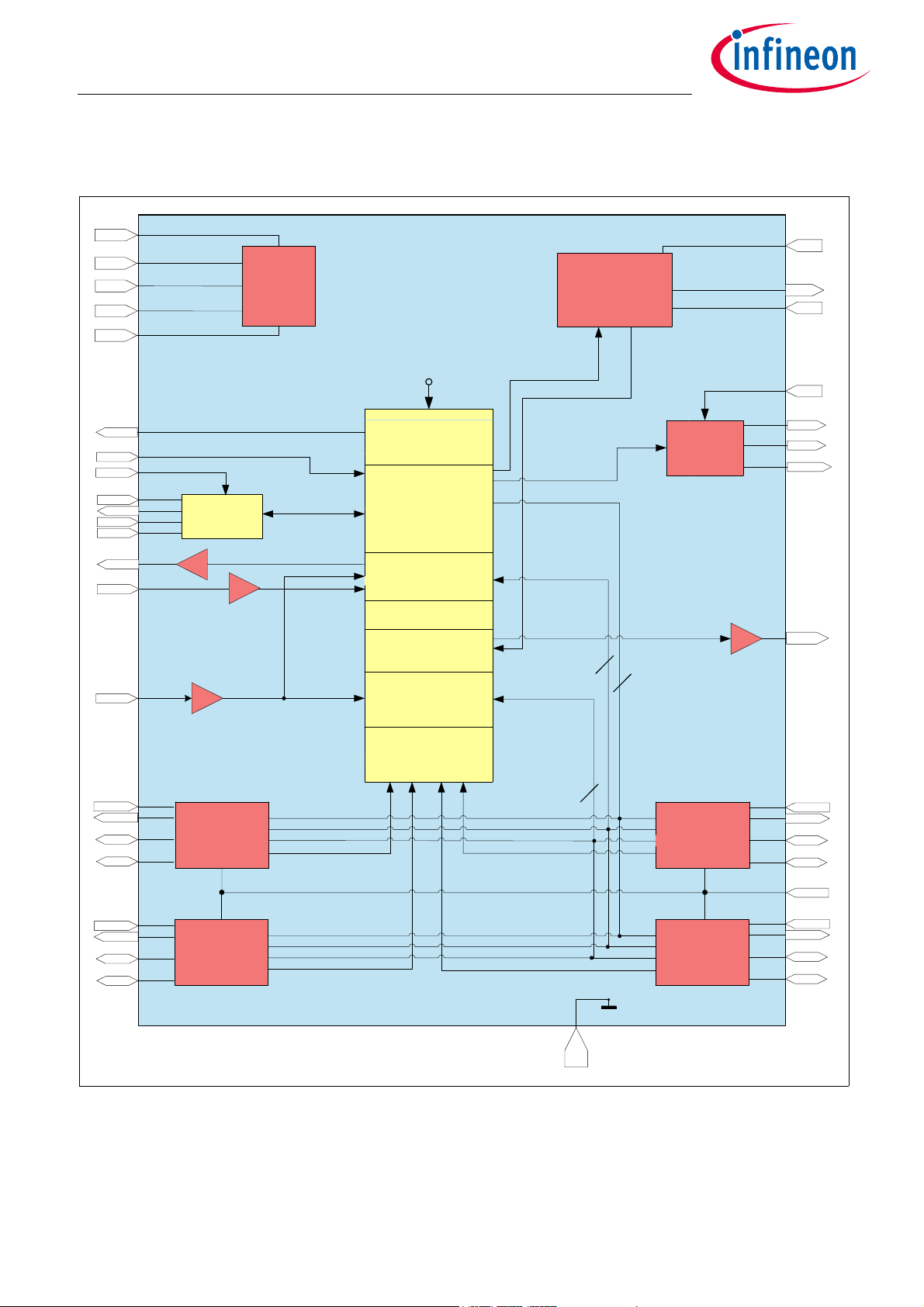
2 Block Diagram
Figure 1 Block Diagram
Datasheet 7 Rev. 1.5
2019-09-27
Page 8

1 CANH0
2 CANL0
3 GND
4 CANL1
5 CANH1
6 GND
7 CANH2
8 CANL2
9 GND
10 CANL 3
11 CANH3
12 PCFG
FO/TEST 48
VEXTREF 47
VEXTB 46
VEXTSH 45
VEXTIN 44
WK 42
GND 41
CLK 40
SDI 39
SDO 38
CSN 37
14 RXDCAN0
15 TXDCAN1
16 RXDCAN1
17 TXDCAN2
18 RXDCAN2
19 VCAN
20 TXDCAN3
21 RXDCAN3
22 VCC1
23 VIO
25 INTN
26 GND
28 n.c.
29 VS
30 VS
31 n.c.
32 GND
33 GND
34 n.c.
35 BSTD
TLE9278
PG-VQFN-48
24 RSTN
13 TX DCAN0
36 BSTD
27 BCKSW
VBSENSE 43
TLE9278-3BQX
Multi-CAN Power+ System Basis Chip
Pin Configuration
3 Pin Configuration
3.1 Pin Assignment
Figure 2 Pin Configuration TLE9278-3BQX
Datasheet 8 Rev. 1.5
2019-09-27
Page 9

TLE9278-3BQX
Multi-CAN Power+ System Basis Chip
Pin Configuration
3.2 Pin Definitions and Functions
Pin Symbol Function
1CANH0 CAN High 0 Bus Pin.
2CANL0 CAN Low 0 Bus Pin.
3 GND Ground. CAN0 and CAN1 common ground.
4CANL1 CAN Low 1 Bus Pin.
5CANH1 CAN High 1 Bus Pin.
6GND Ground. Analog GND.
7CANH2 CAN High 2 Bus Pin.
8CANL2 CAN Low 2 Bus Pin.
9 GND Ground. CAN2 and CAN3 common ground.
10 CANL3 CAN Low 3 Bus Pin.
11 CANH3 CAN High 3 Bus Pin.
12 PCFG Configuration pin. For power up hardware configuration (refer to Chapter 5.1.1).
13 TXDCAN0 Transmit CAN0.
14 RXDCAN0 Receive CAN0.
15 TXDCAN1 Transmit CAN1.
16 RXDCAN1 Receive CAN1.
17 TXDCAN2 Transmit CAN2.
18 RXDCAN2 Receive CAN2.
19 VCAN Supply Input for internal HS-CAN modules.
20 TXDCAN3 Transmit CAN3.
21 RXDCAN3 Receive CAN3.
22 VCC1 Buck Regulator. Input feedback for Buck Converter.
23 VIO I/O voltage supply, reference voltage for over-/undervoltage monitoring
(see Chapter 5.1.1).
24 RSTN Reset Output. Active LOW, internal pull-up.
25 INTN Interrupt Output. Active LOW.
26 GND Ground. Buck regulator ground.
27 BCKSW Buck regulator switch node output.
28 n.c. not connected. Not bondend internally.
29 VS Buck Supply Voltage. Connected to Battery Voltage or Boost output voltage
with reverse protection diode. Use a filter against EMC in case that the Boost is
not used.
30 VS Buck Supply Voltage. Connected to Battery Voltage or Boost output voltage
with reverse protection diode. Use a filter against EMC in case that the Boost is
not used.
31 n.c. not connected. Not bondend internally.
32 GND Ground. Boost regulator ground.
33 GND Ground. Boost regulator ground.
Datasheet 9 Rev. 1.5
2019-09-27
Page 10

TLE9278-3BQX
Multi-CAN Power+ System Basis Chip
Pin Configuration
Pin Symbol Function
34 n.c. not connected. Not bondend internally.
35 BSTD Boost Transistor Drain. Connected between inductor and diode for boost
functionality (refer to Chapter 14.1 for additional information). Connect to
ground if the Boost regulator is not used.
36 BSTD Boost Transistor Drain. Connected between inductor and diode for boost
functionality (refer to Chapter 14.1 for additional information). Connect to
ground if the Boost regulator is not used.
37 CSN SPI Chip Select Not Input.
38 SDO SPI Data Output. Out of SBC (=MISO).
39 SDI SPI Data Input. Into SBC (=MOSI).
40 CLK SPI Clock Input.
41 GND Ground. Common digital ground.
42 WK Wake Input.
43 VBSENSE Battery Voltage Monitoring Input.
44 VEXTIN Input Supply Voltage for VEXT. Connected to Battery Voltage with Reverse
Protection Diode and Filter against EMC.
45 VEXTSH VEXTSH. Emitter connection for external PNP, shunt connection to VEXTIN.
46 VEXTB VEXTB. Base connection for external PNP.
47 VEXTREF VextREF. Collector connection for external PNP, reference input.
48 FO/TEST Fail Output. active LOW, open-drain;
TEST. Connect to GND to activate SBC Development Mode; Integrated pull-up
resistor. Connect to VS with a pull-up resistor or leave open for normal operation.
Cooling
Tab
1) The exposed die pad at the bottom of the package allows better power dissipation of heat from the SBC via the PCB.
The exposed die pad is not connected to any active part of the IC and can be left floating or it can be connected to
GND (recommended) for the best EMC performance.
Note: All VS pins must be connected to battery potential or insert a reverse polarity diodes where required;
GND Cooling Tab - Exposed Die Pad; For cooling purposes only, do not use as an
electrical ground.
All GND pins as well as the Cooling Tab must be connected to one common GND potential.
1)
Datasheet 10 Rev. 1.5
2019-09-27
Page 11

TLE9278-3BQX
Multi-CAN Power+ System Basis Chip
Pin Configuration
3.3 Unused Pins
It must be ensured that the correct configurations are also selected, i.e. in case functions are not used that
they are disabled via SPI:
• CANHx, CANLx, TXDCANx, RXDCANx: leave pins open.
•BSTD: connect to GND.
• WK: connect to GND and disable WK input via SPI.
• RSTN / INTN: leave open.
• FO/TEST: connect to GND during power-up to activate SBC Development Mode; connect to VS or leave
open for normal user mode operation.
• VBSENSE: connect to VS in case that Fast Battery Voltage Monitoring and Boost deactivation features are
not used and keep them disabled.
• VEXT: See Chapter 7.5.
• n.c.: leave open.
• Unused pins routed to an external connector which leaves the ECU should feature a zero ohm jumper
(depopulated if unused) or ESD protection.
Datasheet 11 Rev. 1.5
2019-09-27
Page 12

TLE9278-3BQX
Multi-CAN Power+ System Basis Chip
General Product Characteristics
4 General Product Characteristics
4.1 Absolute Maximum Ratings
Table 1 Absolute Maximum Ratings
1)
Tj = -40°C to +150°C; all voltages with respect to ground, positive current flowing into pin
(unless otherwise specified)
Parameter Symbol Values Unit Note or
Min. Typ. Max.
Test Condition
Voltages
Supply Voltage VS and
V
S1, max
-0.3 – 28 V – P_4.1.1
VEXTIN pin
Supply Voltage VS and
VEXTIN pin
Boost drain Voltage BSTD
V
S2, max
V
BSTD2, max
-0.3 – 40 V Load Dump,
max. 400 ms
-0.3 – 28 V – P_4.1.3
pin
Boost drain Voltage BSTD
pin
Buck switch BCKSW pin V
Buck Regulator feedback,
V
BSTD2, max
BCKSW, max
V
CC1, max
-0.3 – 40 V Load Dump,
max. 400 ms
-0.3 – VS+0.3 V – P_4.1.8
-0.3 – 5.5 V – P_4.1.9
pin VCC1
External Voltage Regulator
(VEXTREF)
V
EXTREF, max
-0.3 – 28 V V
= 40 V for
EXTREF
Load Dump,
max. 400 ms
Number
P_4.1.2
P_4.1.4
P_4.1.26
External Voltage Regulator
(VEXTB)
External Voltage Regulator
(VEXTSH)
Battery Voltage Monitoring V
Wake Input V
Fail Pins FO/TEST V
Interrupt/Configuration Pin
INTN
Configuration Pin PCFG V
Configuration Pin VIO V
CANH, CANL V
Digital Input / Output pin’s V
VCAN Input Voltage V
Maximum Differential CAN
Bus Voltage
V
EXTB, max
V
EXTSH, maxVEXTIN
-0.3 – V
-0.3
VBSENSE,
max
WK, max
HV, max
V
INTN, max
PCFG, max
VIO, max
BUS, max
IO, max
VCAN, max
V
CAN_DIFF,
max
-18 – 40 V – P_4.1.12
-0.3 – 40 V – P_4.1.13
-0.3 – 40 V – P_4.1.14
-0.3 – 5.5 V – P_4.1.15
-0.3 – 40 V – P_4.1.25
-0.3 – 5.5 V – P_4.1.28
-40 – 40 V – P_4.1.16
-0.3 – 5.5 V – P_4.1.17
-0.3 – 5.5 V – P_4.1.18
-5 – 10 V – P_4.1.30
– V
EXTIN
+10
EXTIN
+0.3
V V
= 40 V for
EXTB
Load Dump,
max. 400 ms
V– P_4.1.11
P_4.1.27
Datasheet 12 Rev. 1.5
2019-09-27
Page 13
TLE9278-3BQX
Multi-CAN Power+ System Basis Chip
General Product Characteristics
Table 1 Absolute Maximum Ratings1) (cont’d)
= -40°C to +150°C; all voltages with respect to ground, positive current flowing into pin
T
j
(unless otherwise specified)
Parameter Symbol Values Unit Note or
Min. Typ. Max.
Test Condition
Number
Temperatures
Junction Temperature T
Storage Temperature T
j
stg
-40 – 150 °C – P_4.1.19
-55 – 150 °C – P_4.1.20
ESD Susceptibility
ESD Resistivity to GND V
ESD Resistivity to GND,
ESD
V
ESD
-2 – 2 kV HBM
-8 – 8 kV HBM
2)
2)3)
P_4.1.21
P_4.1.22
CANH, CANL
ESD Resistivity to GND V
ESD Resistivity Pin 1,
12,13,24,25,36,37,48 (corner
ESD
V
ESD1,12,13,2
4,25,36,37,48
-500 – 500 V CDM
-750 – 750 V CDM
4)
4)
P_4.1.23
P_4.1.24
pins) to GND
1) Not subject to production test, specified by design.
2) ESD susceptibility, HBM according to ANSI/ESDA/JEDEC JS-001 (1.5 kΩ, 100 pF).
3) ESD “GUN” Resistivity with ±6 KV (according to IEC61000-4-2 “GUN test” (300 Ω, 150 pF)) it is shown in Application
Information and test will be provided from IBEE institute.
4) ESD susceptibility, Charged Device Model “CDM” EIA/JESD22-C101 or ESDA STM5.3.1, usually not tested but rather
ESD SDM.
Notes
1. Stresses above the ones listed here may cause permanent damage to the device. Exposure to absolute
maximum rating conditions for extended periods may affect device reliability.
2. Integrated protection functions are designed to prevent IC destruction under fault conditions described in the
data sheet. Fault conditions are considered as “outside” normal operating range. Protection functions are
not designed for continuous repetitive operation.
Datasheet 13 Rev. 1.5
2019-09-27
Page 14

TLE9278-3BQX
Multi-CAN Power+ System Basis Chip
General Product Characteristics
4.2 Functional Range
Table 2 Functional Range
Parameter Symbol Values Unit Note or
Test Condition
see section
POR
Supply Voltage V
S,func
Min. Typ. Max.
V
POR
–28V1) V
Number
P_4.2.1
Chapter 12.12
CANx Supply Voltage V
SPI frequency f
CAN
SPI
4.75 – 5.25 V – P_4.2.2
––4MHz see
P_4.2.3
Chapter 13.7 for
f
SPI,max
Junction Temperature T
1) Including Power-On Reset, Over- and Undervoltage Protection.
j
-40 – 150 °C – P_4.2.4
Note: Within the functional range the IC operates as described in the circuit description. The electrical
characteristics are specified within the conditions given in the related electrical characteristics
table.
Device Behavior Outside of Specified Functional Range:
• 28 V < V
< 40 V: Device will still be functional; the specified electrical characteristics might not be
S,func
ensured anymore. The absolute maximum ratings are not violated. However, a thermal shutdown might
occur due to high power dissipation.
• V
< 4.75 V: The undervoltage bit VCAN_UV will be set in the SPI register BUS_STAT_0 and the transmitter
CAN
will be disabled as long as the UV condition is present.
• 5.25 V < V
< 5.5 V: CANx transceiver still functional. However, the communication might fail due to out-
CAN
of-spec operation.
•V
< VS < 5.5 V: Device will be still functional; the specified electrical characteristics might not be ensured
POR,f
anymore:
– The voltage regulators will enter the low-drop operation mode.
– VIO_UV reset could be triggered depending on the VRTx settings.
Datasheet 14 Rev. 1.5
2019-09-27
Page 15
TLE9278-3BQX
Multi-CAN Power+ System Basis Chip
General Product Characteristics
4.3 Thermal Resistance
thJSP
thJA
1)
Number
Min. Typ. Max.
Test Condition
–7 –K/WExposed PadP_4.3.1
–33–K/W
2)
P_4.3.2
Table 3 Thermal Resistance
Parameter Symbol Values Unit Note or
Junction to Soldering Point R
Junction to Ambient R
1) Not subject to production test, specified by design.
2) According to Jedec JESD51-2,-5,-7 at natural convection on FR4 2s2p board for 1.5 W. Board: 76.2 × 114.3 × 1.5 mm3
with 2 inner copper layers (35 µm thick), with thermal via array under the exposed pad . Top and bottom layers are
70 µm thick.
4.4 Current Consumption
Table 4 Current Consumption
Current consumption values are specified at T
(unless otherwise specified)
Parameter Symbol Values Unit Note or
SBC Normal Mode
= 25°C, VS = 13.5 V, all outputs open
j
Min. Typ. Max.
Number
Test Condition
Normal Mode current
consumption
SBC Stop Mode
Stop Mode current
Consumption
Stop Mode current
Consumption, T
= 85°C
j
I
Normal
I
Stop,25
I
Stop,85
– 1016mAVS = 5.5 V to 28 V;
T
= -40°C to +150°C;
j
BOOST/VEXT/CANx =
OFF
– 5570µA1) Buck in PFM
BOOST/VEXT = OFF;
No load on VCC1
VBSENSE_EN = 0
CANx/WK not wake
capable
Watchdog = OFF
–95–µA2) Tj = 85°C;
Buck in PFM
BOOST/VEXT = OFF;
No load on VCC1
VBSENSE_EN = 0
CANx/WK not wake
capable
Watchdog = OFF
P_4.4.1
P_4.4.2
B
P_4.4.3
B
SBC Sleep Mode
Sleep Mode current
consumption
I
Sleep,25
– 3050µABOOST/VEXT = OFF;
VBSENSE_EN = 0
P_4.4.4
B
CANx/WK not wake
capable
Datasheet 15 Rev. 1.5
2019-09-27
Page 16

TLE9278-3BQX
Multi-CAN Power+ System Basis Chip
General Product Characteristics
Table 4 Current Consumption (cont’d)
Current consumption values are specified at T
(unless otherwise specified)
= 25°C, VS = 13.5 V, all outputs open
j
Parameter Symbol Values Unit Note or
Test Condition
BOOST/VEXT = OFF;
Sleep Mode current
consumption, T
= 85°C
j
I
Sleep,85
Min. Typ. Max.
–65–µA2) Tj = 85°C;
VBSENSE_EN = 0
CANx/WK not wake
capable
Feature Incremental Current Consumption
Current consumption per
CAN module, recessive state
I
CAN,rec
–23mASBC Normal Mode;
CAN Normal Mode;
V
= 5 V;
CAN
V
TXDCAN
no RL on CANx
Current consumption per
CAN module, dominant
state
I
CAN,dom
–34.5mA2) SBC Normal Mode;
CAN Normal Mode;
V
= 5 V;
CAN
V
TXDCAN
no RL on CANx
Current consumption per
CAN module, Receive Only
Mode, SBC Normal Mode
I
CAN,RcvOnly,N
M
–0.40.6mA2) CAN Receive Only
Mode; V
V
TXDCAN
no RL on CANx
= VIO;
= GND;
= 5 V;
CAN
= VIO;
Number
P_4.4.5
B
P_4.4.6
P_4.4.7
P_4.4.8
Current consumption per
CAN module, Receive Only
Mode, SBC Stop Mode
Current consumption during
CAN Partial Networking
frame detect mode for one
CAN module
Current consumption during
CAN Partial Networking
frame detect mode for one
CAN module
I
CAN,RcvOnly,St
M
I
CAN,SWK,25
I
CAN,SWK,85
–11.4mA2) CAN Receive Only
Mode; V
V
TXDCAN
= 5 V;
CAN
= VIO;
no RL on CANx
– 700 790 µA
2)3)4)
Tj = 25°C;
VEXT = OFF;
WK not wake
capable;
CAN SWK wake
capable, SWK
Receiver enabled,
WUF detect;
no RL on CANx
– 750 830 µA
2)3)4)
Tj = 85°C;
VEXT= OFF;
WK not wake
capable;
CAN SWK wake
capable, SWK
Receiver enabled,
WUF detect;
no RL on CANx
P_4.4.25
P_4.4.9
P_4.4.10
Datasheet 16 Rev. 1.5
2019-09-27
Page 17

TLE9278-3BQX
Multi-CAN Power+ System Basis Chip
General Product Characteristics
Table 4 Current Consumption (cont’d)
Current consumption values are specified at T
(unless otherwise specified)
= 25°C, VS = 13.5 V, all outputs open
j
Parameter Symbol Values Unit Note or
Test Condition
2)
Tj = 25°C; SBC Stop
Mode; VEXT = OFF;
WK not wake
capable;
Current consumption during
CAN Partial Networking
frame detect mode per
additional CAN module
I
CAN,SWK2,25
Min. Typ. Max.
– 250 300 µA
CAN SWK wake
capable, WUF
detect;
no RL on CANx
Current consumption for WK
wake capability
Current consumption for WK
wake capability T
= 85°C
j
I
Wake,WK,25
I
Wake,WK,85
–0.51.5µA
–2.04.0µA
4)5)
SBC Sleep Mode;
CANx = OFF
2)4)5)
SBC Sleep Mode;
T
= 85°C;
j
CANx = OFF
Current consumption for
CAN wake capability
Current consumption for
CAN wake capability
I
Wake,CAN,25
I
Wake,CAN,85
–4.56µA
–610µA
1)4)
SBC Sleep Mode;
WK = OFF
t
SILENCE
1)2)4)
SBC Sleep Mode;
= 85°C;
T
j
WK = OFF
t
SILENCE
Current consumption for
VEXT in SBC Sleep Mode
I
Sleep,VEXT,25
– 4560µA4) SBC Sleep Mode;
VEXT = ON (no load);
CANx / WK = OFF
Current consumption for
VEXT in SBC Sleep Mode,
= 85°C
T
j
I
Sleep,VEXT,85
– 5570µA
2)4)
SBC Sleep Mode;
= 85°C; VEXT = ON
T
j
(no load);
CANx / WK = OFF
Current consumption for
cyclic wake function
Current consumption for
cyclic wake function,
= 85°C
T
j
Current consumption for
watchdog active in Stop
I
Stop,C25
I
Stop,C85
I
Stop,WD25
– 2026µA
– 2435µA
– 2026µA2) SBC Stop Mode;
4)6)
SBC Stop Mode;
WD = OFF
2)4)6)
SBC Stop Mode;
= 85°C;
T
j
WD = OFF
Watchdog running
Mode
Number
P_4.4.22
P_4.4.11
P_4.4.12
P_4.4.13
expired
P_4.4.14
expired
P_4.4.15
P_4.4.16
P_4.4.17
P_4.4.18
P_4.4.19
Current consumption for
watchdog active in Stop
Mode
Current consumption for
active fail output (FO)
I
Stop,WD85
I
Stop,FO
– 2435µA2) SBC Stop Mode;
T
= 85°C;
j
Watchdog running
–0.51.5mA2) All SBC Modes;
= 25°C;
T
j
P_4.4.20
P_4.4.21
FO = ON (no load);
Datasheet 17 Rev. 1.5
2019-09-27
Page 18

TLE9278-3BQX
Multi-CAN Power+ System Basis Chip
General Product Characteristics
Table 4 Current Consumption (cont’d)
Current consumption values are specified at T
(unless otherwise specified)
= 25°C, VS = 13.5 V, all outputs open
j
Parameter Symbol Values Unit Note or
Min. Typ. Max.
Current consumption Fast
I
Stop,FBM
–5–µA2) SBC Stop Modes;
Battery Monitoring in SBC
Stop Mode
Additional V
current
S
I
BOOST,ON
– 1020mA2) SBC Normal / Stop
consumption with Boost
Module Active
1) Current consumption for CANx transceiver and WK input to be added if set to be wake capable or receiver only.
2) Not subject to production test, specified by design.
3) Current consumption adder applies during WUF detection (frame detect mode) when CAN Partial Networking is
activated. The current consumption will be reduced per module when multiple CAN transceivers are activated for
SWK.
4) Current consumption adders of features defined for SBC Sleep Mode also apply for SBC Stop Mode and vice versa
(unless otherwise specified).
5) No pull-up or pull-down configuration selected.
6) Cyclic wake configuration: Timer with 20 ms period.
Test Condition
VBSENSE_EN = 1
Tj = 25°C;
Modes;
V
< VS< V
BSTx
BOOST_EN = 1
BST,thx
B
Number
P_4.4.30
B
P_4.4.31
;
Datasheet 18 Rev. 1.5
2019-09-27
Page 19

TLE9278-3BQX
Multi-CAN Power+ System Basis Chip
System Features
5 System Features
This chapter describes the system features and behavior of the TLE9278-3BQX:
• State machine and SBC mode control.
• Device configurations.
• State of supply and peripherals.
• Wake features.
• Supervision and diagnosis functions.
The System Basis Chip is controlled via a 16-bit SPI interface. A detailed description can be found in
Chapter 13. The configuration as well as the diagnosis is handled via the SPI. The SPI mapping of the TLE9278-
3BQX is compatible to other devices of TLE926x and TLE927x family.
The System Basis Chip (SBC) offers six operating modes:
• SBC Init Mode: power-up of the device and after soft reset.
• SBC Normal Mode: the main operating mode of the device.
• SBC Stop Mode: the first-level power saving mode with the main voltage regulator enabled.
• SBC Sleep Mode: the second-level power saving mode with Buck regulator disable.
• SBC Restart Mode: an intermediate mode after a wake event from SBC Sleep or SBC Fail-Safe Mode or after
a failure (e.g. WD failure in config 1/3) to bring the microcontroller into a defined state via a reset. Once the
failure condition is not present anymore, the device will automatically change to SBC Normal Mode after a
delay time (t
• SBC Fail-Safe Mode: a safe-state mode after critical failures (e.g. TSD2 thermal shutdown) to bring the
system into a safe state and to ensure a proper restart of the system. Buck regulator is disabled.
A special mode called SBC Development Mode is available during software development or debugging of the
system. All of the operating modes mentioned above can be accessed in this mode. However, the watchdog
counter is stopped and does not need to be triggered. This mode can be accessed by setting the TEST pin to
GND during SBC Init Mode.
RD1
).
5.1 State Machine Description and SBC Mode Control
The different SBC Modes are selected via SPI by setting the respective SBC MODE bits in the register
M_S_CTRL.
The SBC MODE bits are cleared when going trough SBC Restart Mode, so the current SBC mode is always
shown.
Figure 3Figure 4 shows the SBC State Diagram.
Datasheet 19 Rev. 1.5
2019-09-27
Page 20
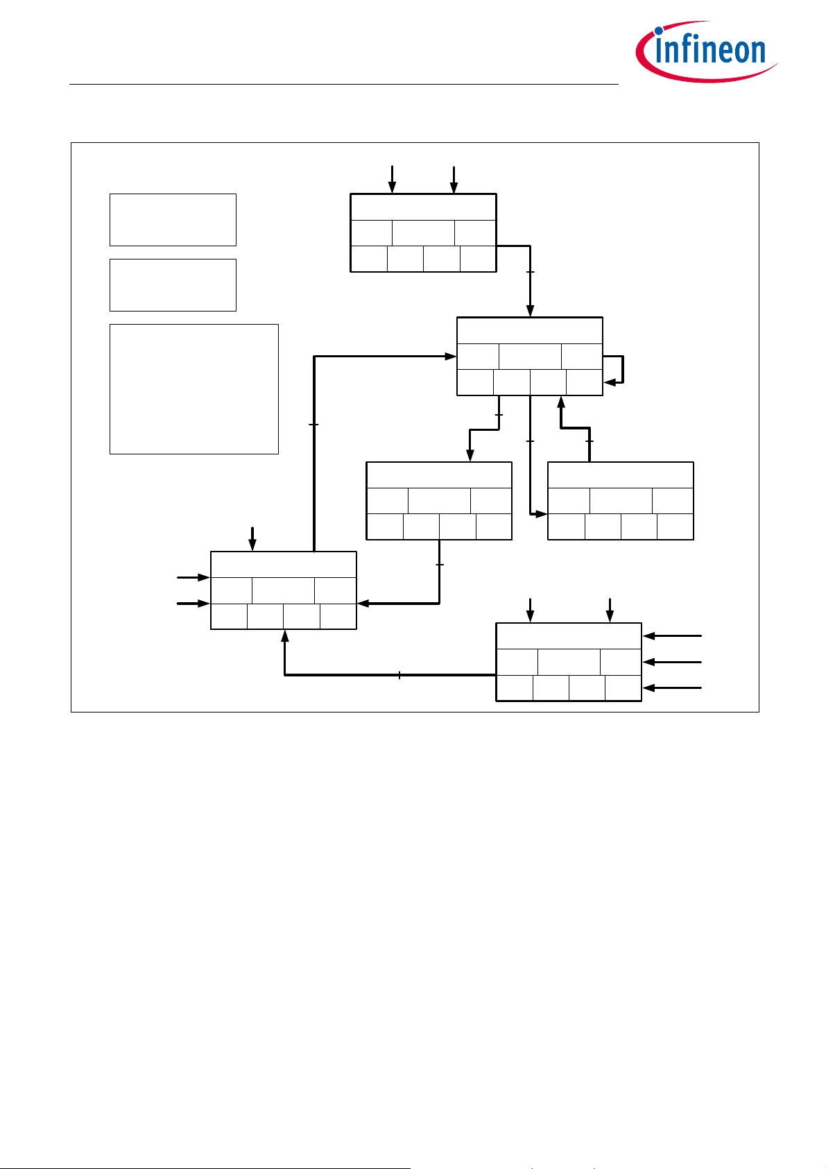
SBC Init Mode
*
(Long open window )
VCC1
ON
(2)
FO
inact.
CAN
OFF
(3)
Wake up event
via CANx or WK
Any SPI
command
SPI cmd
WD trigger
First battery connection
VIO Undervolta ge
Automatic
SBC Soft Reset
§ Reset is released
§ WD starts with long open window
(1) After Fail-Safe Mode entry, the device will stay for at least
typ. 1s in this mode (with RO low) after a TSD2 event and min.
typ. 100ms af ter other Fail -Safe Ev ents. Only t hen the dev ice
can l eave the mode via a wake -up event. Wake ev ents are
stored during this time .
(2) The behaviour depends of the PCFG configuration . If PCFG
is open, the VEXT is by default off and it can be acivated from
the µC with one of the four configurable output voltages . If
PCFG = GND, the VEXT follows the VCC1 in the state machine
with fixed output voltage value at 3.3V.
(3) Fo r SBC Developm ent Mode C AN is in N ormal Mode in
SBC Init Mode and will stay ON when going from there to SBC
Normal Mode
(4) See chapter CAN for detailed behavior in SBC Restart Mode
(5) CA N transceiver can be SWK capab le , depending on
configurat ion
(6) Th e Boost regul ator activati on depends from the VS value .
SBC Normal Mode
FO
act/inact
CAN
Config.
(3)
Boost
(6)
conf./OFF
SBC Restart Mode
(RO pin is as serted)
Config.: settings can be configur ed in
this SBC mode;
Fixed: set tings stay as defined in
SBC Normal Mode
*
The SBC Development Mode is a
super set of state machi ne where the
WD ti mer is stopped and CANx
behavior differs in SBC Init Mode.
Otherwi se, there are no diff erences in
behavior ( see also Chapter 5.1.7).
Cyc.Wake
OFF
Cyc.Wake
config .
CANx, WK wake-up event
VIO over v oltage
Config 1/3 (if VIO_OV_RST set)
Watc hdog Failure :
Config 1/3 (MAX_3_RST not set)
& 1st WD failure in Config4
Boost
OFF
VEXT
(2)
def.
by PCFG pin
VCC1
(2)
ON
VEXT
(2)
def.
by PCFG pin
SBC Stop Mode
Cyc.Wake
fixed
Boost
(6)
fixed/OFF
CAN
(5)
fixed
FO
fixed
VCC1
(2)
ON
VEXT
(2)
def.
by PCFG pin
SBC Sleep Mode
Boost
OFF
Cyc.Wake
OFF
CAN
(5)
Wake
cap./OFF
FO
fixed
VCC1
OFF
SPI cmd
SPI cmd
1st W atchdog Failure Config 2,
2nd Watchdog F ailure, Config 4
VIO Short to GND
SBC Fail-Saf e Mode
(1)
TSD2 event
VIO over volt age
Config 2/4 (if VIO_OV_RST set)
4th consec utive VIO
under vol tage ev ent
(if VS > VS_UV_TO)
VCC1
OFF
FO
fixed
Boost
OFF
VEXT
OFF
Cyc.Wake
OFF
CAN
Wake
capable
VCC1
(2)
ON
VEXT
(2)
def.
by PCFG pin
Boost
(6)
fixed/OFF
FO
active /
fixed
Cyc.Wake
OFF
CAN
(4)
Woken /
OFF
VEXT
(2)
def.
by PCFG pin
WD
Config.
WD
Config.
WD
OFF
WD
fixed
WD
OFF
WD
OFF
TLE9278-3BQX
Multi-CAN Power+ System Basis Chip
System Features
Figure 3 State Diagram showing the SBC Operating Modes
Datasheet 20 Rev. 1.5
2019-09-27
Page 21

SBC Init Mode
*
(Long open window )
VCC1
ON
(2)
FO
inact.
CAN
OFF
(3)
Wake up event
via CANx or WK
Any SPI
command
SPI cmd
WD trigger
First battery connection
VIO Undervolta ge
Automatic
SBC Soft Reset
§ Reset is released
§ WD starts with long open window
(1) After Fail-Safe Mode entry, the device will stay for at least
typ. 1s in this mode (with RO low) after a TSD2 event and min.
typ. 100ms af ter other Fail -Safe Ev ents. Only t hen the dev ice
can l eave the mode via a wake -up event. Wake ev ents are
stored during this time .
(2) The behaviour depends of the PCFG configuration . If PCFG
is open, the VEXT is by default off and it can be acivated from
the µC with one of the four configurable output voltages . If
PCFG = GND, the VEXT follows the VCC1 in the state machine
with fixed output voltage value at 3.3V.
(3) Fo r SBC Developm ent Mode C AN is in N ormal Mode in
SBC Init Mode and will stay ON when going from there to SBC
Normal Mode
(4) See chapter CAN for detailed behavior in SBC Restart Mode
(5) Th e Boost regul ator activati on depends from the VS value .
SBC Normal Mode
FO
act/inact
CAN
Config.
(3)
Boost
(5)
conf./OFF
SBC Restart Mode
(RO pin is as serted)
Config.: settings can be configur ed in
this SBC mode;
Fixed: set tings stay as defined in
SBC Normal Mode
*
The SBC Development Mode is a
super set of state machi ne where the
WD ti mer is stopped and CANx
behavior differs in SBC Init Mode.
Otherwi se, there are no diff erences in
behavior ( see also Chapter 5.1.7).
Cyc.Wake
OFF
Cyc.Wake
config .
CANx, WK wake-up event
VIO over v oltage
Config 1/3 (if VIO_OV_RST set)
Watc hdog Failure :
Config 1/3 (MAX_3_RST not set)
& 1st WD failure in Config4
Boost
OFF
VEXT
(2)
def.
by PCFG pin
VCC1
(2)
ON
VEXT
(2)
def.
by PCFG pin
SBC Stop Mode
Cyc.Wake
fixed
Boost
(5)
fixed/OFF
CAN
fixed
FO
fixed
VCC1
(2)
ON
VEXT
(2)
def.
by PCFG pin
SBC Sleep Mode
Boost
OFF
Cyc.Wake
OFF
CAN
Wake
cap./OFF
FO
fixed
VCC1
OFF
SPI cmd
SPI cmd
1st W atchdog Failure Config 2,
2nd Watchdog F ailure, Config 4
VIO Short to GND
SBC Fail-Saf e Mode
(1)
TSD2 event
VIO over volt age
Config 2/4 (if VIO_OV_RST set)
4th consec utive VIO
under vol tage ev ent
(if VS > VS_UV_TO)
VCC1
OFF
FO
fixed
Boost
OFF
VEXT
OFF
Cyc.Wake
OFF
CAN
Wake
capable
VCC1
(2)
ON
VEXT
(2)
def.
by PCFG pin
Boost
(5)
fixed/OFF
FO
active /
fixed
Cyc.Wake
OFF
CAN
(4)
Woken /
OFF
VEXT
(2)
def.
by PCFG pin
WD
Config.
WD
Config.
WD
OFF
WD
fixed
WD
OFF
WD
OFF
TLE9278-3BQX
Multi-CAN Power+ System Basis Chip
System Features
Figure 4 State Diagram showing the SBC Operating Modes
Datasheet 21 Rev. 1.5
2019-09-27
Page 22

TLE9278-3BQX
Multi-CAN Power+ System Basis Chip
System Features
5.1.1 Device Configuration and SBC Init Mode
The SBC Init Mode is the mode where the hardware configuration of the SBC is stored and where the
microcontroller finishes the initialization phase.
The SBC starts up in SBC Init Mode after crossing the power-on reset V
and the watchdog will start with a long open window (t
typical 200ms) after the RSTN is released.
LW
threshold (see also Chapter 12.3)
POR,r
During this power-on phase following configurations are stored in the device:
• Supply and Power up configurability.
• The device behavior regarding a watchdog trigger failure and a VIO overvoltage condition is determined by
the external circuitry on the INTN pin (see below).
• The selection of the normal device operation or the SBC Development Mode (watchdog disabled for
debugging purposes) will be set depending on the voltage level of the FO/TEST pin (see also
Chapter 5.1.7).
5.1.1.1 Supply and Power up configurability
The TLE9278-3BQX has the possibility to define the level of the digital IO’s using a dedicated pin (VIO). A
separate pin (PCFG) is available to store the I/O supply voltage configuration during power-up. The respective
configuration will be stored for all conditions and can only be changed by powering down the device (V
).
V
POR,f
Depending of the configuration, the supervision functions can refer to VCC1 or VEXT.
The Table 5 shows the only allowed combinations and related behavior.
Table 5 Supply and power up Configurability
<
S
VCC1
Output
PCFG pin VIO Supply µC Supply VEXT
Output voltage
VEXT
Behavior
Supervision
Functions
Voltage
V
= 5 V Open VCC1 VCC1 Configurable via
CC1
SPI using
VEXT_VCFG
SPI
configurable,
OFF after Power
Up
Supervision
functions on VIO
with 5 V level;
VREG_UV SPI
status bit active
V
= 5 V GND VEXT VEXT V
CC1
= 3.3 V
EXT
(fixed)
Follow the VCC1
(ON at Power up
/SBC Normal /
Stop / Sleep /
Fails-Safe Mode)
Supervision
functions on VIO
with 3.3 V level;
VREG_UV status
not active but
rerouted to VCC1
Note: VIO can be connected only to VCC1 or VEXT.
5.1.1.2 Watchdog trigger failure configuration
There are four different device configurations (Table 6) available defining the watchdog failure and the VIO
overvoltage behavior. The configurations can be selected via the external connection on the INTN pin and the
SPI bit CFG2 in the HW_CTRL_0 register (see also Chapter 13.4):
• A watchdog trigger failures leads to SBC Restart Mode (Config 1/3) and depending on CFG2 the Fail Output
(FO) are activated after the 1st or 2nd watchdog trigger failure;
Datasheet 22 Rev. 1.5
2019-09-27
Page 23
TLE9278-3BQX
Multi-CAN Power+ System Basis Chip
System Features
If VIO_OV_RST is set and in Config 1/3, then SBC Restart Mode will be entered in case of VIO_OV and the
FO is activated.
• A watchdog trigger failures leads to SBC Fail-Safe Mode (Config 2/4) and depending on CFG2 the Fail
Output (FO) are activated after the 1st or 2nd watchdog trigger failure. The first watchdog trigger failure in
Config 4 will lead to SBC Restart Mode;
If VIO_OV_RST is set and in Config 2/4, then SBC Fail-Safe Mode will be entered in case of VIO_OV and the
FO is activated.
The respective device configuration can be identified by reading the SPI bits CFG2_STATE and CFG1_STATE
in the WK_LVL_STAT register.
Table 6 Watchdog Trigger Failure Configuration
Config Event FO Activation SBC Mode Entry SPI Bit CFG2 INTN Pin
(CFG1_STATE)
1 1 × Watchdog Failure after 1st WD Failure SBC Restart Mode 1 External pull-up
2 1 × Watchdog Failure after 1st WD Failure SBC Fail-Safe Mode 1 No ext. pull-up
3 2 × Watchdog Failure after 2nd WD Failure SBC Restart Mode 0 External pull-up
4 2 × Watchdog Failure after 2nd WD Failure SBC Fail-Safe Mode 0 No ext. pull-up
The respective configuration will be stored for all conditions and can only be changed by powering down the
device (V
< V
S
POR,f
).
Table 7 shows the possible SBC hardware configurations.
Table 7 SBC Configuration
Configuration Description FO/Test
Pin
Config 0 SBC Development Mode: no reset is
0- XX
triggered in case of watchdog trigger
failure. After the Power Up, one
arbitrary SPI command must be sent.
Config 1 After missing the WD trigger for the first
time, the state of VCC1 remains
Open or
>V
TEST,H
unchanged, FO pin is active, SBC in
Restart Mode
INTN Pin
(CFG1_ST
ATE)
External
pull-up to
V
IO
CFG2_STATECFG1_STA
TE
11
Config 2 After missing the WD trigger for the first
time,VCC1 turns OFF, FO pin are active,
Open or
>V
TEST,H
Open or
GND
10
SBC in Fail-Safe mode
Config 3 After missing the WD trigger for the
second time, the state of VCC1 remains
unchanged, FO pin is active, SBC in
Open or
>V
TEST,H
External
pull-up to
V
IO
01
Restart Mode
Config 4 After missing the WD trigger for the
second time,VCC1 turns OFF, FO pin is
Open or
>V
TEST,H
Open or
GND
00
active, SBC in Fail-Safe mode
Datasheet 23 Rev. 1.5
2019-09-27
Page 24
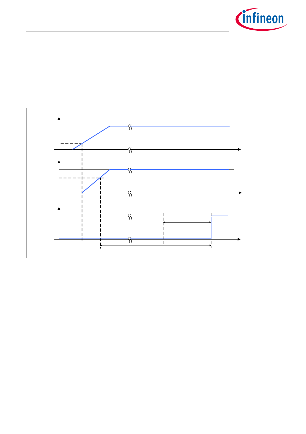
t
VIO
t
RSTN
t
VS
V
POR,r
t
RD1
V
RT1,r
t
CFG_F
Configuration selection monitoring period
Config Select filter time
TLE9278-3BQX
Multi-CAN Power+ System Basis Chip
System Features
In case of 3 consecutive resets due to WD fail, it is possible in Config 1 and 3 not to generate additional reset
by setting the MAX_3_RST on WD_CTRL.
Figure 5 shows the timing diagram of the hardware configuration selection. The hardware configuration is
defined during SBC Init Mode. The INTN pin is internally pulled LOW with a weak pull-down resistor during the
reset delay time t
INTN pin is monitored during this time and the configuration (depending on the voltage level at INTN) is read
and stored at the rising edge of RSTN (with a filter time of t
, i.e. after VIO crosses the reset threshold VRT1 and before the RSTN pin goes HIGH. The
RD1
).
CFG_F
Figure 5 Hardware Selection Timing Diagram
Note: If the POR bit is not cleared then the internal pull-down resistor will be reactivated every time RSTN
is pulled LOW the configuration will be updated at the rising edge of RSTN. Therefore it is
recommended to clear the POR bit right after initialization.
5.1.1.3 SBC Init Mode
In SBC Init Mode, the device waits for the microcontroller to finish its startup and initialization sequence. In
the SBC Init Mode any SPI command will bring the SBC to SBC Normal Mode. During the long open window
the watchdog has to be triggered. Thereby the watchdog will be automatically configured. A missing
watchdog trigger during the long open window will cause a watchdog failure and the device will enter SBC
Restart Mode.
Wake events are ignored during SBC Init Mode and will therefore be lost.
Note: Any SPI command will bring the SBC to SBC Normal Mode even if non-valid (see Chapter 13.2).
Note: For a safe start-up, it is recommended to use the first SPI command to trigger and to configure the
watchdog (see Chapter 12.2).
Datasheet 24 Rev. 1.5
2019-09-27
Page 25

TLE9278-3BQX
Multi-CAN Power+ System Basis Chip
System Features
RT1
RT1
, the
Note: At power up, no VIO_UV will be issued nor will FO be triggered as long as VIO is below the V
threshold and V
low as long as VIO is below the selected V
RSTN is released after t
is below the VIO short circuit detection threshold V
S
threshold. As soon as the VIO is higher than V
RT1
.
RD1
. The RSTN pin will be kept
S,UV
5.1.2 SBC Normal Mode
The SBC Normal Mode is the standard operating Mode for the SBC. All configurations have to be done in SBC
Normal Mode before entering a low-power mode (see also Chapter 5.1.6 for the device configuration defining
the Fail-Safe Mode behavior). A wake-up event on CANx and WK will create an interrupt on pin INTN however,
no change of SBC Mode will occur. The configuration options are listed below:
• VCC1 is active, Buck in PWM Mode.
• VEXT can be switched ON or OFF in accordance with Table 5.
• CANx is configurable (OFF coming from SBC Init Mode; OFF or wake capable coming from SBC Restart
Mode, see also Chapter 5.1.5).
• Wake pin level can be monitored and can be selected to be wake capable.
• Cyclic wake period can be configured using TIMER_CTRL_0 and enabled by setting TIMER1_WK_ EN.
• Watchdog is configurable.
• FO is OFF by default.
In SBC Normal Mode, there is the possibility of testing the FO output, i.e. to verify if setting the FO pin to low
will create the intended behavior within the system. The FO output can be enabled and then disabled again
by the microcontroller by setting the FO_ON SPI bit. This feature is only intended for testing purposes.
5.1.3 SBC Stop Mode
The SBC Stop Mode is the first level technique to reduce the overall current consumption. All kind of settings
have to be done before entering SBC Stop Mode. In SBC Stop Mode any kind of SPI write commands are
ignored and the SPI_FAIL bit is set, except for changing to SBC Normal Mode, triggering a SBC Soft Reset,
refreshing the watchdog, changing modulation of the buck. The configuration options are listed below:
• VCC1 is ON, Buck in PFM Mode if I
• VEXT is fixed ON or OFF in accordance with Table 5 and SPI configuration.
• CANx can be selected for ‘Receive Only Mode’, to be wake capable or OFF.
• WK pin can be selected to be wake capable, PWM_BY_WK (switch PFM/PWM buck modulation) or OFF.
• Wake capability via cyclic wake can be selected.
• Watchdog is fixed or OFF (if WD disable sequence was executed).
A wake-up event on CANx and WK will create an interrupt on pin INTN however, no change of SBC Mode will
occur.
In SBC Stop Mode, it is allowed to use the Boost module (enabled before to enter in SBC Stop Mode) in case of
the V
is dropping. The Boost works only in PWM and therefore the total amount of current consumption will
S
increase.
Note: It is not possible to switch directly from SBC Stop Mode to SBC Sleep Mode. Doing so will also set the
SPI_FAIL flag and will bring the SBC into Normal Mode via SBC Restart Mode.
VCC1
< I
PFM-PWM,TH
.
Datasheet 25 Rev. 1.5
2019-09-27
Page 26

TLE9278-3BQX
Multi-CAN Power+ System Basis Chip
System Features
5.1.4 SBC Sleep Mode
The SBC Sleep Mode is the second level technique to reduce the overall current consumption to a minimum
needed to react on wake-up events.
All settings must be done before entering SBC Sleep Mode. In case that SPI configurations in Sleep Mode have
been sent to the SBC, the commands are ignored and no reactions from the SBC.
The configuration options are listed below:
•VCC1 is OFF.
• VEXT is fixed ON or OFF in accordance with Table 5 and SPI configuration.
• CANx can be selected to be wake capable or OFF.
• WK pin can be selected to be wake capable or OFF.
A wake-up event on CANx or WK pin will bring the device via SBC Restart Mode into SBC Normal Mode again
and signal the wake event and corresponding sources.
It is not possible to switch off all wake sources in Sleep Mode. This will lead to SBC Normal Mode via SBC
Restart Mode instead.
In order to enter SBC Sleep Mode successfully, all wake source signalization flags from WK_STAT_0 and
WK_STAT_2 need to be cleared. If a failure to do so, will result in an immediate wake-up from SBC Sleep Mode
by going via SBC Restart to Normal Mode.
Note: As soon as the Sleep Command is sent, the Reset will go low to avoid any undefined behavior
between SBC and microcontroller.
5.1.5 SBC Restart Mode
There are multiple reasons to enter the SBC Restart Mode. The purpose of the SBC Restart Mode is to reset the
microcontroller:
• From SBC Normal and Stop Mode, it is reached in case of undervoltage on VIO. In case of 4 consecutive
VIO_UV events, SBC Fail-Safe Mode is entered.
• From SBC Normal and Stop Mode it is reached in case of overvoltage on VIO in config 1/3 if VIO_OV_RST is
set.
• Incorrect Watchdog triggering (depending of the configuration).
• From SBC Sleep and Fail-Safe Mode to ramp up VIO supply after wake event.
From SBC Restart Mode, the SBC goes automatically to SBC Normal Mode, i.e the mode is left automatically
by the SBC without any microcontroller influence once the VIO_UV condition is not present anymore and
when the reset delay time (t
Entering or leaving the SBC Restart Mode will not result in deactivation of the Fail output.
The following functions are not changed in SBC Restart mode:
• VEXT is fixed ON or OFF in accordance with Table 5 and SPI configuration.
• VCC1 is ON or ramping up.
) has expired. The Reset Output (RSTN) is released at the transition.
RD1
•BOOST is fixed or OFF.
Table 8 contains detailed descriptions of the reason to restart:
Datasheet 26 Rev. 1.5
2019-09-27
Page 27
TLE9278-3BQX
Multi-CAN Power+ System Basis Chip
System Features
Table 8 Reasons for Restart - State of SPI Status Bits after Return to Normal Mode
SBC Mode Event DEV_STAT WD_FAIL VIO_UV VIO_OV
Normal Watchdog Failure 01 01 x x
Normal VIO undervoltage reset 01 xx 1 x
Normal VIO overvoltage (VIO_OV_RST=1) 01 xx x 1
Sleep Mode Wake-up event 10 xx x x
Stop Mode Watchdog Failure 01 01 x x
Stop Mode VIO undervoltage reset 01 xx 1 x
Stop Mode VIO overvoltage (VIO_OV_RST=1) 01 xx x 1
Fail-Safe Wake-up event 01 see “Reasons for Fail-Safe, Table 9”
5.1.6 SBC Fail-Safe Mode
The purpose of this mode is to bring the system in a safe status after a failure condition by turning off the VCC1
and VEXT supply and the FO pin is automatically activated. After a wake-up event the system is then able to
restart again.
The Fail-Safe Mode is automatically reached in case of:
• Overtemperature condition (TSD2).
• After 1 or 2 watchdog fails (depending on config setting).
• At the 4th consecutive VIO undervoltage event.
• From SBC Normal and Stop Mode, in case of overvoltage on VIO in config 2/4, if VIO_OV_RST is set.
• VIO is shorted to GND.
• VIO is below the VRTx for time longer than t
In this case, the default wake sources are activated, the wake-up events are cleared in the register WK_STAT_0
and WK_STAT_2.
The mode will be maintained for at least t
to avoid any fast toggling behavior. All wake sources will be masked during this time but the wake-up events
will be stored. Stored wake-up events and wake-up event after this minimum waiting time, will lead to SBC
Restart Mode. Leaving the SBC Fail-Safe Mode will not result in deactivation of the Fail Output pin.
The following functions are influenced during SBC Fail-Safe Mode:
• FO output is activated.
•VCC1 is OFF.
VIO,SC
in case of TSD2 event and t
TSD2
.
in case of other failure events
FS,min
• VEXT is OFF.
•CANx is wake capable.
•WK is wake capable (in case that PWM_BY_WK was set, moving to SBC Fail-Safe Mode will clear the bit).
•Cyclic wake is disabled.
Table 9 Reasons for Fail-Safe - State of SPI Status Bits after Return to Normal Mode
Mode Config Event DEV_STAT TSD2 WD_FAIL VIO_UV VIO_SC VIO_OV
Normal 2 1 × watchdog
failure
Normal 4 2 × watchdog
failure
Datasheet 27 Rev. 1.5
01 x 01 x 0 x
01 x 10 x 0 x
2019-09-27
Page 28

TLE9278-3BQX
Multi-CAN Power+ System Basis Chip
System Features
Table 9 Reasons for Fail-Safe - State of SPI Status Bits after Return to Normal Mode (cont’d)
Mode Config Event DEV_STAT TSD2 WD_FAIL VIO_UV VIO_SC VIO_OV
Normal 1, 2, 3, 4 TSD2 01 1 xx x 0 x
Normal 1, 2, 3, 4 VIO short to GND 01 x xx 1 1 x
Normal 2, 4 VIO overvoltage
(VIO_OV_RST=1,
CFG2=1)
Stop Mode 2 1 × watchdog
failure
Stop Mode 4 2 × watchdog
failure
Stop Mode 1, 2, 3, 4 TSD2 01 1 xx x 0 x
Stop Mode 1, 2, 3, 4 VIO short to GND 01 x xx 1 1 x
Stop Mode 2, 4 VIO overvoltage
(VIO_OV_RST=1,
CFG2=1)
01 x xx x 0 1
01 x 01 x 0 x
01 x 10 x 0 x
01 x xx x 0 1
5.1.7 SBC Development Mode
The SBC Development Mode is used during development phase of the application, especially for software
development.
Compared to the default SBC user mode operation, this mode is a super set of the state machine. The device
will start also in SBC Init Mode and it is possible to use all the SBC Modes and functions with following
differences:
• Watchdog is stopped and does not need to be triggered. Therefore no reset is triggered due to watchdog
failure.
• SBC Fail-Safe and Restart Mode are not reached due to watchdog failure but the other reasons to enter
these modes are still valid.
• CANx default value in SBC INIT MODE is ON instead of OFF.
The mode is reached by setting the FO/TEST pin to LOW for the entire SBC INIT Mode and by sending an
arbitrary SPI command. The SBC Init Mode is reachable after the power-up or sending a software reset.
SBC Development Mode can only be left by a power-down or by providing a SBC Software Reset using the
MODE bits on M_S_CTRL register regardless the FO/TEST pin level.
When the FO/TEST pin is left open, or connected to V
operation. The FO/TEST pin has an integrated pull-up resistor (switched ON only during SBC Init Mode) to
prevent the SBC device from starting in SBC Development Mode during normal life of the vehicle. To avoid any
disturbances, the FO/TEST pin is monitored during the SBC Init Mode when the RSTN is HIGH until SBC Init
Mode is left. Only if the FO/TEST pin is LOW for the Init Mode time when the RSTN is HIGH, SBC Development
Mode is reached and stored.
during the start-up, the SBC starts into normal
S
Datasheet 28 Rev. 1.5
2019-09-27
Page 29
Cyclic Wake Configuration
Cyclic Wake starts / ends by
setting / clearing On-time
INT is pulled low at every rising edge
of On-time except first one
Select Timer Period in
TIMER_CTRL_0
Periods: 10 , 20 , 50, 100, 200ms, 1s, 2s
Reset the TIMER1_WK_EN bit on
WK_CTRL_0 register
To avoid unintentional inter rupts
Set the TIMER1_WK_EN bit on
WK_CTRL_0 register
No interrupt will be generated,
if the timer is not enabled as a wake source
TLE9278-3BQX
Multi-CAN Power+ System Basis Chip
System Features
5.2 Wake Features
Following wake sources are implemented in the device:
• Static Sense: WK input is permanently active (see Chapter 9).
• Cyclic Wake: internal wake source controlled via internal timer (see Chapter 5.2.1).
• CANx wake: wake-up via CAN message (see Chapter 8).
The wake source must be set before entering in SBC Sleep Mode. In case of critical situation, when the device
will be set into SBC Fail-Safe mode, all default wake sources will be activated. For additional information
about setting, refer to the respective chapters.
5.2.1 Cyclic Wake
The cyclic wake feature is intended to reduce the quiescent current of the device and application.
When the cyclic wake is enabled, a periodic INTN is generated in SBC Normal and Stop Mode based on the
setting of TIMER_CTRL_0.
The correct sequence to configure the cyclic wake is shown in Figure 6. The sequence is as follows:
• Disable the cyclic wake feature to ensure that there is not unintentional interrupt when activating cyclic
wake (TIMER1_WK_ EN = 0).
• Configure the cyclic wake timer period in TIMER_CTRL_0 register.
• Enable the cyclic wake as a wake-up source in the register WK_CTRL_0 (TIMER1_WK_ EN = 1).
Figure 6 Cyclic Wake: Configuration and Sequence
5.2.2 Internal Timer
The integrated timer is typically used to wake up the microcontroller periodically (cyclic wake).
Following periods can be selected via the register TIMER_CTRL_0:
• Period: 10ms / 20ms / 50ms / 100ms / 200ms / 1s / 2s
Datasheet 29 Rev. 1.5
2019-09-27
Page 30

TLE9278-3BQX
Multi-CAN Power+ System Basis Chip
5.3 CAN Partial Networking
5.3.1 CAN Partial Networking - Selective Wake Feature
The CAN Partial Networking feature can be activated for SBC Normal Mode, in SBC Sleep Mode and in SBC Stop
Mode. For SBC Sleep Mode the Partial Networking has to be activated before sending the SBC to Sleep Mode.
For SBC Stop Mode the Partial Networking has to be activated before going to SBC Stop Mode.
There are 2 detection mechanism available:
• WUP (Wake-Up Pattern) this is a CAN wake, that reacts on the CAN dominant time, with 2 dominant signals
as defined in ISO WG11898-6.
• WUF (Wake-Up frame) this is the wake-up on a CAN frame that matches the programmed message filter
configured in the SBC via SPI.
The default baud rate is set to 500 kBaud. Besides the commonly used baud rate of 125 kBaud and 250 kBaud,
other baud rate up to 1 MBaud can be selected (see Chapter 13.5.2 and Chapter 13.6.2 for more details).
Datasheet 30 Rev. 1.5
2019-09-27
Page 31

CAN
Normal Mode
Config Check
CAN
Wake detection
(WUP)
CAN WUF
detection
tsilence
CAN Protocoll Error
Counter
not valid
N-1 N+
N>32
max. 4
CAN frames
CAN
WUF
N>0
CAN PN
CAN WK Mode
without PN
CAN
OFF
CAN Wakable Mode
CAN Woken UP
1)
Sleep Mode: SBC goes to Restart Mode,
RxD is low, SPI bits are set
Stop Mode: SBC stays in Stop Mode,
Interrupt is triggered, RxD is low, SPI bits
are set
valid
Normal Mode: SBC stays in Normal Mode,
Interrupt is triggered, SPI bits are set, RxD
is low (only in case of CAN WK or SWK
Mode, not in Receive Only with SWK or
CAN Normal Mode with SWK)
CAN Receive Only
Mode
CAN Wake
WUP
SPISPI
SPISPI
CAN Wake
WUP
SPI
CAN frame error
detection
Enable/ Disable
CAN WUP
detection
Error counter
overvlow
SYSERR
N = 0
rearming
N = 0
Tsilent
1)
CFG_VAL is cleared in
Reast art M ode
SYSERR
TLE9278-3BQX
Multi-CAN Power+ System Basis Chip
5.3.2 SBC Partial Networking Function
The CAN Partial Networking Modes are shown in Figure 7.
Figure 7 CAN Selective Wake State Diagram
Datasheet 31 Rev. 1.5
2019-09-27
Page 32

CANx
Enable CAN
Enabling CANx (not OFF ) enables also
the selective wake block. Block gets
synchronous to the CAN bus .
If one CAN Frame is rec eived the bit
SYNC_x = 1 is set
Set SWK wake data . e.g.
ID, ID_Mask, DATA
Set
CFG_VAL = 1
Bit set to confirm by the microcontroller
that valid data are programmed .
Setting the data can als o be done as
first task
SYNC_x = 1
SBC N ormal Mode
SW not enabled
CAN OFF
SYSERR_x
1
0
SWK not enabled
In cas e SWK not enabled :
CANx Normal with SW -> CANx Normal
CANx Rx Only with SW -> CANx Rx Only
CANx Wak able with SW -> CANx Wakable
SBC Sleep Mode
SBC Stop Mode
INTN generation
stay s in SBC Stop Mode
MODE = 10
To ensure that no wak e -up ev ent
has tak en place in meantime
In cas e of WUF detection :
CAN_x_WU = 1; WUF_x = 1;
CFG_VAL = 0; SWK_ SET_x = 0
Handle wak e
event
(incl. CAN
mode toggling )
Clear
SYSERR_x
Enable a CAN
Mode with SWK
via CANx Bits
CAN Mode must be toggled before
(re-)enabling wake capable mode
Clear
the wake-up status
register related the
selected CANx
To avoid inv alid configuration
Check SWK_STAT_x
Check & C lear
the wake-up status
register related the
selected CANx
To activ ate Selec tive Wake
Selectiv e Wake is now enabled
(INTN is generated in case of WUF )
Notes:
- Tsilenc e handling not s hown i n drawing
- SYNC_x will only be set once CANx is „rearmed“
and at least one CA N f rame was sent succ ess full y
SWK_SET_x = 1,
CAN_x_WUP & WUF_x = 0,
SYNC_x = 1
Select SBC
low-power mode
via MODE Bits
MODE = 01
Wake -up: VCC1 Power-up
change to SBC Normal Mode
TLE9278-3BQX
Multi-CAN Power+ System Basis Chip
5.3.2.1 Activation of SWK
Figure 8 shows the principal of the SWK activation.
Figure 8 Flow for activation of SWK
Datasheet 32 Rev. 1.5
2019-09-27
Page 33

Ini
Bia s off
1
Bia s off
2
Bia s off
3
Bias on
4
Bias on
Wait
Bia s off
Bus recessive > t
WAKE1
Bus dominant > t
WAKE1
optional:
t
WAKE2
expired
Bus recessive > t
WAKE1
Bus dominant > t
WAKE1
Bus recessive > t
WAKE1
Bus dominant > t
WAKE1
optional:
t
WAKE2
expired
t
Silence
expired AND
Device in low-power mode
t
Silence
expired AND
device in low-power mode
Entering CAN Normal
or CAN Recive Only
Entering low -pow er mode ,
when selective wake-up
function is dis abled
or not supported
TLE9278-3BQX
Multi-CAN Power+ System Basis Chip
5.3.2.2 Wake-up Pattern (WUP)
A WUP is signaled on the bus by two consecutive dominant bus levels for at least t
recessive bus level.
, each separated by a
Wake1
Figure 9 WUP detection following the definition in ISO 11898-5
5.3.2.3 Wake-up Frame (WUF)
The wake-up frame is defined in ISO11898-6.
Only CAN frames according ISO11898-1 are considered as potential wake-up frames.
A bus wake-up shall be performed, if selective wake-up function is enabled and a “valid WUF” has been
received. The transceiver may ignore up to four consecutive CAN data frames that start after switching on the
bias.
A received frame is a “valid WUF” in case all of the following conditions are met:
• The ID of the received frame is exactly matching a configured ID in the relevant bit positions. The relevant
• The DLC of the received frame is exactly matching the configured DLC.
• In case DLC is greater than 0, the data field of the received frame has at least one bit set in a bit position,
• No error exists according to ISO 11898-1 excepting errors which are signalled in the ACK field and EOF field.
bit positions are given by an ID mask. The ID and the ID mask might have either 11 bits or 29 bits.
where also in the configured data mask in the corresponding bit position the bit is set.
Datasheet 33 Rev. 1.5
2019-09-27
Page 34

TLE9278-3BQX
Multi-CAN Power+ System Basis Chip
5.3.2.4 CAN Protocol Error Counter
The counter is incremented when a bit stuffing, CRC or form error according to ISO11898-1 is detected. If a
frame has been received that is valid up to the end of the CRC field and the counter is not zero, the counter is
decremented. If the counter has reached a value of 31, the following actions is performed on the next
increment of this counter:
• The selective wake function is disabled.
• The CANx transceiver is woken.
• SYSERR_x is set and the error counter value = 32 can be read.
On each increment or decrement of the counter the decoder unit waits for at least 6 and most 10 recessive bits
before considering a dominant bit as new start of frame.
The error counter is enabled:
• Whenever the CANx is in Normal Mode, Receive Only Mode or in WUF detection state.
The error counter is cleared under the following conditions:
• At the transition from WUF detection to WUP detection 1 (after t
enabled).
• When WUF detection state is entered (in this way the counter will start from 0 when SWK is enabled).
• At SBC or CANx rearming (when exiting the woken state).
• When the CANx Mode bits are selected ‘000’, ‘100’ (CANx OFF) or ‘001’ (CANx Wake Capable without SWK
function enabled).
•While CAN_FD_EN = ‘1’ and DIS_ERR_CNT = ‘1’ (the counter is cleared and stays cleared when these two
bits are set in the SPI registers).
The Error Counter us frozen:
• After a wake-up being in woken state.
The counter value can be read out of the bits ECNT_x_0 to ECNT_x_5.
expiration, while SWK is correctly
SILENCE
Datasheet 34 Rev. 1.5
2019-09-27
Page 35

TLE9278-3BQX
Multi-CAN Power+ System Basis Chip
5.3.3 Diagnoses Flags
5.3.3.1 PWRON/RESET-FLAG
The power-on reset can be detected and read by the POR bit in the SBC Status register.
The VS power on resets all register in the SBC to reset value. SWK is not configured.
5.3.3.2 BUSERR-Flag
Bus Dominant Time-out detection is implemented and signaled by CAN_x_Fail bits in the status register
related the selected CAN transceiver (BUS_STAT_0 or BUS_STAT_2 or BUS_STAT_3).
5.3.3.3 TxD Dominant Time-out flag
TxD Dominant Time-out is shown in the SPI bit CAN_x_FAIL in register in the status register related the
selected CAN transceiver.
5.3.3.4 WUP_x Flag
The WUP_x bit in the SWK_STAT_x register shows that a Wake-Up Pattern (WUP) has caused a wake of the CAN
transceiver. It can also indicate an internal mode change from WUP detection to WUF detection after a valid
WUP.
In the following case the bit is set:
• SWK is activated: due to t
the WUP_x bit is set.
• SWK is deactivated: the WUP_x bit is set if a WUP wakes up the CAN. In addition, the CAN_x_WU bit is set.
• In case WUP is detected during WUP detection 2 state (after a SYSERR_x) the bits WUP_x and CAN_x_WU
are set.
The WUP_x bit is cleared automatically by the SBC at the next rearming of the CAN transceiver.
Note: It is possible that WUF and WUP bit are set at the same time if a WUF causes a wake out of SWK, by
setting the interrupt or by restart out of SBC Sleep Mode. The reason is because the CAN has been in
WUP detection mode during the time of SWK mode (because of t
, the CAN goes into WUP detection. If a WUP is detected in this state, then
SILENCE
). See also Figure 10.
SILENCE
5.3.3.5 WUF Flag (WUF_x)
The WUF_x bit in the SWK_STAT_x register shows that a Wake-Up frame (WUF) has caused a wake of the CANx
block. In SBC Sleep Mode this wake causes a restart, in SBC Normal Mode and in SBC Stop Mode it causes an
interrupt. Also in case of this wake the bit CAN_x_WU in the register WK_STAT_x is set.
The WUF_x bit is cleared automatically by the SBC at the next rearming of the CAN SWK function.
5.3.3.6 SYSERR Flag (SYSERR_x)
The bit S YSERR_x is set in ca se of an configuration error and in case of an error counter overflow. The bit is only
updated (set to 1) if a CANx mode with SWK is enabled via CANx bits.
When programming selective wake via CANx, SYSERR_x = 0 signals that the SWK function has been enabled.
The bit can be cleared via SPI. The bit is ‘0’ after Power on reset of the SBC.
Datasheet 35 Rev. 1.5
2019-09-27
Page 36

TLE9278-3BQX
Multi-CAN Power+ System Basis Chip
5.3.3.7 Configuration Error
A configuration error sets the SYSERR_x bit to 1. When enabling SWK via the bits CANx a config check is done.
If the check is successful SWK is enabled, the bit SYSERR_x is set to 0. In SBC Normal Mode it is also possible to
detect a Configuration Error while SWK is enabled, this will happen if the CFG_VAL bit is cleared, e.g. by
changing the SWK register (from address 010 0001 to address 011 0011). In SBC Stop Mode and SBC Sleep
Mode this is not possible as the SWK registers can not be changed.
Configuration Check:
in SBC Restart Mode, the CFG_VAL bit is cleared by the SBC. If the SBC Restart Mode was not triggered by a
WUF wake up from SBC Sleep Mode and the CAN was with SWK enabled, than the SYSERR_x bit will be set.
The SYSERR_x bit has to be cleared by the microcontroller.
The SYSERR_x bit cannot be cleared when CANx_2 is ‘1’ and below conditions occur:
• Data Valid bit not set by the microcontroller, e.g. CFG_VAL is not set to ‘1’. The CFG_VAL bit is reset after
SWK wake and needs to be set by the microcontroller before activation SWK again.
• CFG_VAL bit reset by the SBC when data are changed via SPI programming. (Only possible in SBC Normal
Mode).
Note: The SWK configuration is still valid if only the SWK_CTRL register is modified.
5.3.3.8 CAN BUS Time-out-Flag (CANTO_x)
In CAN WUF detection and CAN WUP detection 2 state, the bit CANTO_x is set to 1 if the time t
The bit can be cleared by the microcontroller. If the interrupt function for CANTO_x is enabled an Interrupt is
generated in SBC Stop and SBC Normal Mode when the CANTO_x set to 1. The interrupt is enabled by setting
the bit CANTO_MASK to 1. Each CANTO_x event will trigger a interrupt even if the CANTO_x bit is not cleared.
There is no wake out of SBC Sleep Mode because of CAN time-out.
SILENCE
expires.
5.3.3.9 CAN BUS Silence-Flag (CANSIL_x)
In CAN WUF detection and CAN WUP detection 2 state the bit CANSIL_x is set to ‘1’ if the time t
The CANSIL_x bit is set back to ‘0’ with a WUP. With this bit the microcontroller can monitor if there is activity
on the CAN bus while being in SWK Mode. The bit can be read in SBC Stop and Normal Mode.
SILENCE
expires.
5.3.3.10 SYNC-FLAG (SYNC_x)
The bit SYNC_x shows that SWK is working and synchronous to the CAN bus. To get a SYNC_x bit set it is
required to enable the CAN (CANx bits), no CAN Mode with SWK needs to be enabled.
The bit is set to 1 if a valid CAN frame has been received. It is set back to 0 if a CAN protocol error is detected.
When switching into SWK mode the SYNC_x bit indicates to the µC that the frame detection is running and the
next CAN frame can be detected as a WUF, CAN wake-up can now be handled by the SBC. It is possible to enter
a SBC low-power mode with SWK even if the bit is not set to 1, as this is necessary in case of a silent bus.
5.3.3.11 SWK_SET FLAG (SWK_SET_x)
The status bit SWK_SET_x is set to signalize the following states (see also Figure 7):
• When SWK was correctly enabled in WUF Detection state.
• When SWK was correctly enabled when WUP Detection 1 state.
• After a SYSERR_x before a wake event in WUP Detection 2 state.
The bit is cleared if following conditions:
Datasheet 36 Rev. 1.5
2019-09-27
Page 37

CAN OFF Mode
CAN WK Mode
CAN Normal Mode
(no SWK)
CAN Normal mode
CAN Normal mode with SWK
Config.
Check
CAN
SWK
SPI CAN_x
CAN RX Only Mode
CAN RX Only Mode with SWK
Config.
Check
Config.
Check
CAN
SWK
CAN Wakable Mode
with SWK
CAN Receive-Only
Mode
OKOK
OK
CAN WK
CAN
SWK
CAN WKCAN WK
Not OK Not OK Not OK
TLE9278-3BQX
Multi-CAN Power+ System Basis Chip
•After a wake-up (ECNT_x overflow, WUP_x in WUP detection 2, WUF_x in WUF detection).
•If CANx_2 is cleared.
5.3.4 SBC Modes for Selective Wake (SWK)
The SBC mode is selected via the MODE bits as described in Chapter 5.1.
The mode of the CAN transceiver needs to be selected in SBC Normal Mode. The CAN mode is programed the
bits CANx_0, CANx_1 and CANx_2. In the low-power modes (SBC Stop and Sleep Mode) the CAN mode can not
be changed via SPI.
The detailed SBC state machine diagram including the CAN selective wake feature is shown in Figure 3.
The application must now distinguish between the normal CAN operation an the selective wake function:
• WK Mode: This is the normal CAN wake capable mode without the selective wake function.
• SWK Mode: This is the CAN wake capable mode with the selective wake function enabled.
Figure 10 shows the possible CAN transceiver modes.
Figure 10 CAN SWK State Diagram
5.3.4.1 SBC Normal Mode with SWK
In SBC Normal Mode the CANx Transceiver can be switched into the following CAN Modes:
•CAN OFF
• CAN WK Mode (without SWK)
•CAN SWK Mode
• CAN Receive Only (No SWK activated)
• CAN Receive Only Mode with SWK
• CAN Normal Mode (No SWK activated)
Datasheet 37 Rev. 1.5
2019-09-27
Page 38

TLE9278-3BQX
Multi-CAN Power+ System Basis Chip
• CAN Normal Mode with SWK
In the CAN Normal Mode with SWK the CANx Transceiver works as in SBC Normal Mode, so bus data is received
through RXDCANx, data is transmitted through TXDCANx and sent to the bus. In addition the SWK block is
active. It monitors the data on the CAN bus, updates the error counter and sets the CANSIL_x flag if there is no
communication on the bus.
It will generate an CAN Wake interrupt in case a WUF is detected (RXDCANx is not pulled to LOW in this
configuration).
In CAN Receive Only Mode with SWK, CAN data can be received on RXDCANx and SWK is active, no data can be
sent to the bus.
The bit SYSERR_x = 0 indicates that the SWK function is enabled, and no frame error counter overflow is
detected.
Table 10 CAN Modes selected via SPI in SBC Normal Mode
CAN Mode CANx_2 CANx_1 CANx_0
CAN OFF 000
CAN WK Mode (no SWK) 001
CAN Receive Only (no SWK) 0 1 0x
CAN Normal Mode (no SWK) 0 1 1
CAN OFF 100
CAN SWK Mode 101
CAN Receive Only with SWK 1 1 0
CAN Normal Mode with SWK 1 1 1
When reading back CAN_x the programmed mode is shown in SBC Normal Mode. To read the real CAN mode
the bits SYSERR_x, SWK_SET_x and CAN_x have to be evaluated. A change out of SBC Normal Mode can
change the CAN_x_0 and CAN_x_1 bits.
5.3.4.2 SBC Stop Mode with SWK
In SBC Stop Mode the CANx Transceiver can be operated with the following CAN Modes:
•CAN OFF
•CAN WK Mode (no SWK)
•CAN SWK Mode
• CAN Receive Only (no SWK)
To enable CAN SWK Mode the CANx has to be switched to “CAN Normal Mode with SWK”, “CAN Receive Only
Mode with SWK” or to “CAN SWK Mode” in SBC Normal Mode before sending the SBC to SBC Stop Mode. The
bit SYSERR_x = 0 indicates that the SWK function is enabled. The table shows the change of CAN Mode when
switching from SBC Normal Mode to SBC Stop Mode.
Note: CAN Receive Only Mode in SBC Stop Mode is implemented to also enable pretended networking
(Partial networking done in the microcontroller).
Datasheet 38 Rev. 1.5
2019-09-27
Page 39

TLE9278-3BQX
Multi-CAN Power+ System Basis Chip
Table 11 CAN Modes change when switching from SBC Normal Mode to SBC Stop Mode
Programmed CAN Mode in SBC
Normal Mode
CAN OFF 000 0 CAN OFF 000
CAN WK Mode (no SWK) 001 0 CAN WK Mode (no SWK) 001
CAN Receive Only (no SWK) 010 0 CAN Receive Only (no SWK) 010
CAN Normal Mode (no SWK) 011 0 CAN WK Mode (no SWK) 001
CAN OFF 100 0 CAN OFF 100
CAN SWK Mode 101 0 CAN SWK Mode 101
CAN SWK Mode 101 1 CAN WK Mode (no SWK) 101
CAN Receive Only with SWK 110 0 CAN Receive Only with SWK 110
CAN Receive Only with SWK 110 1 CAN Receive Only (no SWK) 110
CAN Normal Mode with SWK 111 0 CAN WK Mode with SWK 101
CAN Normal Mode with SWK 111 1 CAN WK Mode (no SWK) 101
Note: When SYSERR_x is set it is true that we will not detect WUF frames, so no selective wake function
active (no SWK), but the MSB of CAN mode is not changed in the register.
CANx
Modes
SYSERR_
x bit
CAN Mode in SBC Stop Mode CANx
Modes
5.3.4.3 SBC Sleep Mode with SWK
In SBC Sleep Mode the CANx Transceiver can be switched into the following CAN Modes:
•CAN OFF
• CAN WK Mode (without SWK)
•CAN SWK Mode
To enable “CAN SWK Mode” the CAN has to be switched to “CAN Normal Mode with SWK”, “CAN Receive Only
Mode with SWK” or to “CAN SWK Mode” in SBC Normal Mode before sending the device to SBC Sleep Mode.
The table shows the change of CAN mode when switching from SBC Normal Mode to Sleep Mode.
A wake from Sleep Mode with Selective Wake (Valid WUF) leads to SBC Restart Mode. In SBC Restart Mode the
CFG_VAL bit will be cleared by the SBC, the SYSERR_x bit is not set. In the BUS_CTRL_x register, the
programmed CAN SWK Mode (101) can be read.
To enable the CAN SWK Mode again and to enter SBC Sleep Mode the following sequence can be used;
Program a CAN Mode different from CAN SWK Mode (101, 110, 111), set the CFG_VAL, clear SYSERR_x bit, set
CANx transceiver to CAN SWK Mode (101), switch SBC to SBC Sleep Mode.
To enable the CAN WK Mode or CAN SWK Mode again after a wake on CANx, a rearming is required. The
rearming is done by programming the CANx transceiver into a different mode and back into the CAN WK Mode
or CAN SWK Mode. To avoid lock-up when switching the SBC into SBC Sleep Mode with an already woken CANx
transceiver, the SBC does an automatic rearming of the CANx transceiver when switching into Sleep Mode. So
after switching into SBC Sleep Mode the CANx transceiver is either in CAN SWK Mode or CAN WK Mode
depending on CANx_2 setting and SYSERR_x bit (If CAN is switched to OFF Mode it is also OFF in Sleep Mode)
Datasheet 39 Rev. 1.5
2019-09-27
Page 40

TLE9278-3BQX
Multi-CAN Power+ System Basis Chip
Table 12 CAN Modes change when switching to SBC Sleep Mode
Programmed CAN Mode in SBC
Normal Mode
CAN OFF 000 0 CAN OFF 000
CAN WK Mode (no SWK) 001 0 CAN WK Mode (no SWK) 001
CAN Receive Only (no SWK) 010 0 CAN WK Mode (no SWK) 001
CAN Normal Mode (no SWK) 011 0 CAN WK Mode (no SWK) 001
CAN OFF 100 0 CAN OFF 100
CAN SWK Mode 101 0 CAN SWK Mode 101
CAN SWK Mode 101 1 CAN WK Mode (no SWK) 101
CAN Receive Only with SWK 110 0 CAN SWK Mode 101
CAN Receive Only with SWK 110 1CAN WK Mode (no SWK) 101
CAN Normal Mode with SWK 111 0 CAN SWK Mode 101
CAN Normal Mode with SWK 111 1 CAN WK Mode (no SWK) 101
CANx
Modes
SYSERR_
x bit
CAN Mode in SBC Sleep Mode CANx
Modes
5.3.4.4 SBC Restart Mode with SWK
If SBC Restart Mode is entered the transceiver can change the CAN mode. During Restart or after Restart the
following modes are possible:
•CAN OFF
• CAN WK Mode (either still wake cable or already woken up)
• CAN SWK Mode (WUF Wake from Sleep)
Table 13 CAN Modes change in case of Restart out of SBC Normal Mode
Programmed CAN Mode in SBC
Normal Mode
CAN OFF 000 0 CAN OFF 000 0
CAN WK Mode (no SWK) 001 0 CAN WK Mode (no SWK) 001 0
CAN Receive Only (no SWK) 010 0 CAN WK Mode (no SWK) 001 0
CAN Normal Mode (no SWK) 011 0 CAN WK Mode (no SWK) 001 0
CAN OFF 100 0 CAN OFF 100 0
CAN SWK Mode 101 0 CAN WK Mode (no SWK) 101 1
CAN SWK Mode 101 1 CAN WK Mode (no SWK) 101 1
CAN Receive Only with SWK 110 0 CAN WK Mode (no SWK) 101 1
CAN Receive Only with SWK 110 1 CAN WK Mode (no SWK) 101 1
CAN Normal Mode with SWK 111 0 CAN WK Mode (no SWK) 101 1
CAN Normal Mode with SWK 111 1 CAN WK Mode (no SWK) 101 1
The various reasons for entering SBC Restart Mode and the respective status flag settings are shown in
Table 14.
CANx
Modes
SYSERR_
x bit
CAN Mode in and after SBC
Restart Mode
CANx
Modes
SYSERR
_x bit
Datasheet 40 Rev. 1.5
2019-09-27
Page 41

TLE9278-3BQX
Multi-CAN Power+ System Basis Chip
Table 14 CAN Modes change in case of Restart out of SBC Sleep Mode
CAN Mode in SBC
Sleep Mode
CAN OFF CAN OFF 0000 0000 Wake on other wake
CAN WK Mode CAN woken up0010 1100 Wake (WUP) on CAN
CAN WK Mode CAN WK Mode00100000 Wake on other wake
CAN SWK Mode CAN woken up 101 0 1 0/1
CAN SWK Mode CAN woken up 101 1 1 0/1
CAN SWK selected,
CAN WK active
CAN SWK Mode CAN WK Mode 101 1 0 0/1 0 x Wake on other wake
1) In case there is a WUF detection within t
together with the WUF_x bit.
2) In some cases the WUP_x bit might stay cleared even after t
detecting a wake up pattern
CAN Mode in
and after SBC
Restart Mode
CAN woken up1011 1100 Wake (WUP) on CAN,
CANx
Modes
SILENCE
SYS
ERR_
x
then the WUP_x bit will not be set. Otherwise it will always be set
CAN_
x_WU
WUP_xWUF_xECNT_
x bits
1)
1 x Wake (WUF) on CAN
2)
0 100000 Wake due to error
, e.g. when the error counter expires without
SILENCE
Reason for Restart
source
source
counter overflow
config check was not
pass
source
5.3.4.5 SBC Fail-Safe Mode with SWK
When SBC Fail-Safe Mode is entered the CAN transceiver is automatically set into WK Mode (wake capable)
without the selective wake function.
5.3.5 Wake-up
A wake-up via CAN leads to a restart out of SBC Sleep Mode and to an interrupt in SBC Normal Mode, and in
SBC Stop Mode. After the wake event the bit CAN_x_WU is set, and the details about the wake can be read out
of the bits WUP_x, WUF_x, SYSERR_x and ECNT_x bits.
5.3.6 Configuration for SWK
The CAN protocol handler settings can be configured in following registers:
• SWK_BTL1_CTRLdefines the number of time quanta in a bit time. This number depends also on the
internal clock settings performed in the register SWK_CDR_CTRL2.
• SWK_BTL2_CTRLdefines the sampling point position.
• The respective receiver during frame detection mode can be selected via the bit RX_WK_SEL.
• The clock and data recovery (see also Chapter 5.3.8.2) can be configured in the registers
SWK_CDR_CTRL1, SWK_CDR_CTRL2, SWK_CDR_LIMIT_HIGH_CTRL and SWK_CDR_LIMIT_LOW_CTRL.
The actual configuration for selective wake is done via the Selective Wake Control Registers SWK_IDx_CTRL,
SWK_MASK_IDx_CTRL, SWK_DLC_CTRL, SWK_DATAx_CTRL.
Datasheet 41 Rev. 1.5
2019-09-27
Page 42

TLE9278-3BQX
Multi-CAN Power+ System Basis Chip
The oscillator has the option to be trimmed by the microcontroller. To measure the oscillator, the SPI bit
OSC_CAL needs to be set to 1 and a defined pulse needs to be given to the TXDCANx pin by the microcontroller
(e.g. 1µs pulse, CANx needs to be switched off before). The SBC measures the length of the pulse by counting
the time with the integrated oscillator. The counter value can be read out of the register
SWK_OSC_CAL_H_STAT and SWK_OSC_CAL_L_STAT. To change the oscillator the trimming function needs
to be enabled by setting the bits TRIM_EN_x = 11 (and OSC_CAL = 1). The oscillator can then be adjusted by
writing into the registers SWK_OSC_TRIM_CTRL and SWK_OPT_CTRL. To finish the trimming, the bits
TRIM_EN_x need to be set back to “00”.
5.3.7 CAN Flexible Data Rate (CAN FD) Tolerant Mode
The CAN FD tolerant mode can be activated by setting the bit CAN_FD_EN = 1 in the register
SWK_CAN_FD_CTRL. With this mode the internal CANx frame decoding will be stopped for CAN FD frame
formats:
• The high baud rate part of a CAN FD frame will be ignored.
• No Error Handling (Bit Stuffing, CRC checking, Form Errors) will be applied to remaining CAN frame Fields
(Data Field, CRC Field, …).
• No wake up is done on CAN FD frames.
The internal CAN frame decoder will be ready for new CAN frame reception when the End of frame (EOF) of a
CAN FD frame is detected.The identification for a CAN FD frame is based on the EDL Bit, which is sent in the
Control Field of a CAN FD frame:
• EDL Bit = 1 identifies the current frame as an CAN FD frame and will stop further decoding on it.
• EDL Bit = 0 identifies the current frame as CAN 2.0 frame and processing of the frame will be continued.
In this way it is possible to send mixed CAN frame formats without affecting the selective wake functionality
by error counter increment and subsequent misleading wake up.In addition to the CAN_FD_EN bit also a filter
setting must be provided for the CAN FD tolerant mode. This filter setting defines the minimum dominant time
for a CAN FD dominant bit which will be considered as a dominant bit from the CAN FD frame decoder. This
value must be aligned with the selected high baud rate of the data field in the CAN network.
To support programming via CAN during CAN FD mode a dedicated SPI bit DIS_ERR_CNT is available to avoid
an overflow of the implemented error counter (see also Chapter 5.3.2.4).
The behavior of the error counter depends on the setting of the bits DIS_ERR_CNT and CAN_FD_EN and is
show in below table:
Table 15 Error Counter Behavior
DIS_ERR_CNT setting CAN_FD_EN setting Error Counter Behavior
0 0 Error Counter counts up when a CAN FD frame or an
incorrect/corrupted CAN frame is received; counts down
when a CAN frame is received properly
(as specified in ISO 11898-6)
1 0 Error Counter counts up when a CAN FD frame or an
incorrect/corrupted CAN frame is received; counts down
when a CAN frame is received properly
(as specified in ISO 11898-6)
Datasheet 42 Rev. 1.5
2019-09-27
Page 43

CDR
80 Mhz Oscilator
(analog )
Aquisition
Filter Fractional
Divider
CAN
Protocoll
Handler
CAN Receiver
(analog)
RX
TLE9278-3BQX
Multi-CAN Power+ System Basis Chip
Table 15 Error Counter Behavior (cont’d)
DIS_ERR_CNT setting CAN_FD_EN setting Error Counter Behavior
0 1 Error Counter counts down when correct CAN (incl. CAN FD)
frame is received
1 1 Error Counter is and stays cleared to avoid an overflow
during programming via CAN
The DIS_ERR_CNT bit is automatically cleared at t
SILENCE
expiration.
5.3.8 Clock and Data Recovery
In order to compensate possible deviations on the CAN oscillator frequency caused by assembly and lifetime
effects, the device features an integrated clock and data recovery (CDR).
It is recommended to always enable the CDR feature during SWK operation.
5.3.8.1 Configuring the Clock Data Recovery for SWK
The Clock and Data Recovery can be optionally enabled or disabled with the CDR_EN Bit in the
SWK_CDR_CTRL1 SPI Register. In case the feature is enabled, the CAN bit stream will be measured and the
internal clock used for the CAN frame decoding will be updated accordingly. Before the Clock and Data
Recovery can be used it must be configured properly related to the used baud rate and filtering characteristics
(refer to Chapter 5.3.8.2).
It is strongly recommended to not enable/disable the Clock Recovery during a active CAN Communication.
To ensure this it is recommended to enable/disable it during CAN OFF.
Figure 11 Clock and Data Recovery Block Diagram
5.3.8.2 Setup of Clock and Data Recovery
It is strongly recommended to enable the clock and data recovery feature only when the setup of the clock and
data recovery is finished.
The following sequence should be followed for enabling the clock and data recovery feature:
• Step 1: Switch CANx to OFF and CDR_EN to OFF
• Step 2: Configure CDR Input clock frequency
Datasheet 43 Rev. 1.5
Write SPI Register BUS_CTRL_x (CANx = 000).
Write SPI Register SWK_CDR_CTRL2 (SEL_OSC_CLK[1:0]).
2019-09-27
Page 44

TLE9278-3BQX
Multi-CAN Power+ System Basis Chip
• Step 3: Configure Bit timing Logic
Write SPI Register SWK_BTL1_CTRL and adjusting SWK_CDR_LIMIT_HIGH_CTRL and
SWK_CDR_LIMIT_LOW_CTRL according to Table 33.
• Step 4: Enable Clock and Data Recovery
Choose filter settings for Clock and Data recovery. Write SPI Register SWK_CDR_CTRL1 with CDR_EN = 1
Additional hints for the CDR configuration and operation:
• Even if the CDR is disabled, when the baud rate is changed, the settings of SEL_OSC_CLK in the register
SWK_CDR_CTRL1 and SWK_BTL1_CTRL have to be updated accordingly.
•The SWK_CDR_LIMIT_HIGH_CTRL and SWK_CDR_LIMIT_LOW_CTRL registers have to be also updated
when the baud rate or clock frequency is changed (the CDR is discarding all the acquisitions and looses all
acquired information, if the limits are reached - the SWK_BTL1_CTRL value is reloaded as starting point
for the next acquisitions).
• When updating the CDR registers, it is recommended to disable the CDR and to enable it again only after
the new settings are updated.
•The SWK_BTL2_CTRL register represents the sampling point position. It is recommended to be used at
default value: 11 0011 (~80%).
Datasheet 44 Rev. 1.5
2019-09-27
Page 45

TLE9278-3BQX
Multi-CAN Power+ System Basis Chip
5.3.9 Electrical Characteristics
Table 16 Electrical Characteristics
V
= 5.5 V to 28 V; Tj = -40°C to +150°C; 4.75 V < V
S
respect to ground, positive current flowing into pin
(unless otherwise specified)
CAN
< 5.25 V; RL = 60 Ω; CAN Normal Mode; all voltages with
Parameter Symbol Values Unit Note or
Min. Typ. Max.
Test Condition
Number
CAN Partial Network Timing
Time-out for bus inactivity t
Bias reaction time t
Wake-up reaction time
(WUP or WUF)
SILENCE
bias
t
WU_WUP/WUF
0.6 – 1.2 s
– – 200 µs
– – 100 µs
1)
1)
Load RL = 60 Ω,
C
= 100 pF,
L
= 100 pF
C
GND
1)2)3)
Wake-up
reaction time
P_5.3.1
P_5.3.2
P_5.3.3
after a valid WUP
or WUF;
Min. Bit Time t
CAN FD Tolerance
5)
SOF acceptance n
Bit_min
Bits_idle
1––µs
6–10bits6)Number of
1)4)
recessive bits
P_5.3.4
P_5.3.5
before a new SOF
shall be accepted
Dominant signals which
are ignored
(up to 2 MBit/s)
t
FD_Glitch_4
0–5%
6)7)8)
arbitration bit
time; to be
of
P_5.3.6
configured via
FD_FILTER;
Dominant signals which
are ignored
(up to 5 MBit/s)
t
FD_Glitch_10
0–2.5%
6)7)9)
of
arbitration bit
time; to be
P_5.3.7
configured via
FD_FILTER;
Signals which are detected
t
FD_DOM_4
17.5 – – %
as a dominant data bit after
the FDF bit and before EOF
bit
(up to 2 MBit/s)
Signals which are detected
t
FD_DOM_10
8.75 – – %
as a dominant data bit after
the FDF bit and before EOF
bit
(up to 5 MBit/s)
1) Not subject to production test, tolerance defined by internal oscillator tolerance.
2) Wake-up is signalized via INTN pin activation in SBC Stop Mode and via VCC1 ramping up with wake from SBC Sleep
Mode.
6)7)8)
of
arbitration bit
time; to be
configured via
FD_FILTER;
6)7)9)
of
arbitration bit
time; to be
configured via
FD_FILTER;
P_5.3.8
P_5.3.9
Datasheet 45 Rev. 1.5
2019-09-27
Page 46

TLE9278-3BQX
Multi-CAN Power+ System Basis Chip
3) For WUP: time starts with end of last dominant phase of WUP; for WUF: time starts with end of CRC delimiter of the
WUF.
4) The minimum bit time corresponds to a maximum bit rate of 1 Mbit/s. The lower end of the bit rate depends on the
protocol IC or the permanent dominant detection circuitry preventing a permanently dominant clamped bus.
5) Applies for an arbitration rate of up to 500 kbps until the FDF bit is detected.
6) Not subject to production test; specified by design.
7) Parameter applies only for the Normal Mode CAN receiver (RX_WK_sel = 0).
8) A data phase bit rate less or equal to four times of the arbitration bit rate or 2 Mbit/s, whichever is lower.
9) A data phase bit rate less or equal to ten times of the arbitration bit rate or 5 Mbit/s, whichever is lower.
Datasheet 46 Rev. 1.5
2019-09-27
Page 47

GND
Buck
Converter
VCC1
BCKSW
VS
Feedforwar d
Soft Star t
Ramp
Generator
Bandgap
Reference
C1 C3
L1
L2
C4
Boost
Converter
Comparator
Logic
SPI
C2
C5
D2
D1
Vbat
BSTD
BSTD
GND
VS
VSUP
GND
Cf1
TLE9278-3BQX
Multi-CAN Power+ System Basis Chip
DC/DC Regulator
6 DC/DC Regulator
6.1 Block Description
The SMPS module in the TLE9278-3BQX is implemented as a cascade of a step-up regulator followed by a stepdown post-regulator. The step-up regulator (DC/DC Boost converter) provides a V
step-down post-regulator (DC/DC Buck converter) to regulate without entering a low-drop condition.
The SMPS module is active in SBC Normal, Stop and Restart Mode. In SBC Sleep and Fail-Safe Mode, the SMPS
module is disabled.
level which permits the
S
Figure 12 DC/DC Block Diagram
Functional Features
• 5 V SMPS (DC/DC) Buck Regulator with integrated high-side and low-side power switching transistor.
• SMPS (DC/DC) Boost Regulator for low V
• Adjustable output DC/DC Boost pre-regulator voltage via SPI.
• Fixed switching frequency for Buck and Boost Regulator in SBC Normal Mode in PWM (Pulse Width
Modulation).
• PFM (Pulse Frequency Modulation) for Buck converter in SBC Stop Mode to reduce the quiescent current.
• Automatic transition PFM to PWM in SBC Stop Mode.
• Soft start-up.
Datasheet 47 Rev. 1.5
supply voltage with integrated power transistor.
SUP
2019-09-27
Page 48

GND
Buck
Converter
VCC1
BCKSW
Feedforward
Soft Start
Ramp
Generator
Bandgap
Reference
L2
C5
Logic
C6
SPI
C1 C3
L1
D1
Vbat
VS
C2
V
SUP
TLE9278-3BQX
Multi-CAN Power+ System Basis Chip
DC/DC Regulator
• Edge Shaping for better EMC performances for Buck and Boost regulator.
• Undervoltage monitoring via VIO pin with adjustable reset level (refer to Chapter 12.7).
• Overvoltage detection via VIO pin activates the FO pin in case that VIO_OV_RST bit is set and if PCFG is
open (refer to Chapter 12.8).
• Buck short circuit detection.
• Buck 100% Duty Cycle at low V
• Buck overcurrent peak detection.
• Boost overcurrent peak detection.
6.1.1 Functional Description of the Buck Converter
operation.
S
Figure 13 Buck Block Diagram
The DC/DC Buck converter is intended as post-regulator (VCC1) and it provides a step down converter function
transferring energy from V
output voltage is 5 V in a current range up to 750 mA. It is regulated via a digital loop with a precision of ±2%.
It requires an external inductor and capacitor filter on the output switching pin (BCKSW). The Buck regulator
has integrated high-side and low-side power switching transistors. The compensation of the regulation loop
is done internally and no additional external components are needed.
A typical application example and external components proposal is available in Chapter 14.1.
The Buck converter is active in SBC Normal, Stop and Restart Mode and it is disabled in SBC Sleep and FailSafe Mode.
Depending on the SBC Mode, the Buck converter works in two different modes:
• PWM Mode (Pulse Width Modulation): This mode is available in SBC Normal Mode, SBC Restart Mode and
SBC Stop Mode (only for automatic or manual PFM to PWM transitions. Refer to Chapter 6.2.2). In PWM,
the Buck converter operates with a fixed switching frequency (f
based on input voltage, output voltage and output current. The precision is ±2% or ±3% based on input
supply and output current range (refer to Figure 18 for more information). In PWM Mode, the Buck
converter is capable of a 100% duty cycle in case of low V
shaping feature has been implemented to control the activation and deactivation of the two power
switches.
Datasheet 48 Rev. 1.5
to a lower output voltage with high efficiency (typically more than 80%). The
S
). The duty cycle is calculated internally
BUK
conditions. In order to reduce EMC, the edge
S
2019-09-27
Page 49

Coil Current
Tristate TristateHS LS
Feedback Voltage VCC 1
PFM active
LVL
UCL
LCL
start biasing
&
oscillator
Quiescent Current
Iq Iq
OFF ON ONOFF
TLE9278-3BQX
Multi-CAN Power+ System Basis Chip
DC/DC Regulator
• PFM Mode (Pulse Frequency Modulation): This mode is activated automatically when the SBC Stop Mode
is entered. The PFM Mode is an asynchronous mode. PFM Mode does not have a controller switching
frequency. The switching frequency depends on conditions of the Buck regulator such as the following:
input supply voltage, output voltage, output current and external components. A typical timing diagram is
shown in Figure 14. The Buck converter in PFM Mode has a tolerance of ±4%. The transition from PFM
mode to PWM mode is described in Chapter 6.2.2.
Figure 14 Typical PFM timing diagram
6.1.1.1 Startup Procedure (Soft Start)
The Startup Procedure (Soft Start) permits to achieve the Buck regulator output voltage avoiding large
overshoot on the output voltage. This feature is activated during the power-up, from SBC Sleep to Restart
Mode and from SBC Fail-Safe to SBC Restart Mode.
When the Buck regulator is activated, it starts in open loop with a minimum duty cycle which is maintained for
a limited number of switching periods. After this first phase, the duty cycle is linearly increased by a fixed step
and it is maintained for a limited number of switching periods for each duty cycle step. This procedure is
repeated until the target output voltage value of the Buck regulator is reached. As soon as the Buck regulator
output voltage is reached, the regulation loop is closed and it starts to operate normally using PWM Mode
adjusting the duty cycle according to the Buck input and output voltages and the output current.
6.1.1.2 Buck regulator Status register
The register SMPS_STAT contains information about the open or short conditions on BCKSW pin. No SBC
Mode or configuration changes are triggered if one bit on SMPS_STAT register is set.
6.1.1.3 External components
The Buck converter needs one inductor and output capacitor filter. The inductor has a fixed value of 47 µH.
Secondary parameters such as saturation current must be selected based on the maximum current capability
needed in the application.
The output filter capacitors are two parallel 22 µF ceramic capacitor. For additional information, refer to
Chapter 14.1.
Datasheet 49 Rev. 1.5
2019-09-27
Page 50

VS
C1 C4
L1
Boost
Converter
Compa rator
Logic
SPI
C3
D2
D1
Vbat
BSTD
BSTD
GND
VS
VSUP
GND
C2
VS
BST_ACT
001
BSTD
VS
VSUP
V
BST,THx
V
BST,HYSx
V
BSTx
TLE9278-3BQX
Multi-CAN Power+ System Basis Chip
DC/DC Regulator
6.1.2 Functional Description of the Boost Converter
Figure 15 Boost Block Diagram
The Boost converter is intended as a pre-regulator and it provides a step up converter function. It transfers
energy from an input supply V
(V
) with high efficiency (typically more than 80%).
S
The regulator integrates the power switching and the sense resistor for overcurrent detection.
(battery voltage after reverse protection circuit) to a higher output voltage
SUP
The Boost regulator can be enabled in SBC Normal Mode via SPI (register HW_CTRL_0, bit BOOST_EN) and
four output voltage values are selectable via BOOST_V. The Boost regulator can also be active in SBC Stop and
Restart Mode. The selected boost output voltage will automatically define the voltage thresholds where the
boost will be ON (V
automatically when V
, V
BST,TH1
falls below the selected threshold voltage and switches OFF when crossing this
S
BST,TH2
, V
BST,TH3
and V
). If the Boost regulator is enabled, it switches ON
BST,TH4
threshold including hysteresis again. The bit BST_ACT on SMPS_STAT register indicates that the Boost has
been activated.
The Boost output voltage can be changed only if BOOST_EN is set to 0. In case that the boost output voltage
configuration changes with BOOST_EN set to 1, the SPI_FAIL bit is set and the command is ignored.
Figure 16 shows the typical timing for enabling the Boost converter.
Figure 16 Boost converter activation
Datasheet 50 Rev. 1.5
2019-09-27
Page 51

TLE9278-3BQX
Multi-CAN Power+ System Basis Chip
DC/DC Regulator
The Boost regulator works in PWM Mode with fixed frequency (f
If the Boost is enabled in Stop Mode, the quiescent current in the SBC is increased (P_4.4.31).
) and a tolerance of ±3%.
BST
6.1.2.1 Boost Regulator Status register
The register SMPS_STAT contains information about the open or short conditions on Boost pins including loss
of GND detection. No SBC mode or configuration is triggered if one bit is set on the SMPS_STAT register.
6.1.2.2 External Components
The Boost converter requires a number of external components such as the following: input buffer capacitor
on the battery voltage, inductor, freewheeling diode and filter capacitors.
For recommend external components and corresponding values, refer to Chapter 14.1.
Datasheet 51 Rev. 1.5
2019-09-27
Page 52

TLE9278-3BQX
Multi-CAN Power+ System Basis Chip
DC/DC Regulator
6.2 Power Scenarios
The chapter describes the features and performance of the Buck regulator according to SBC modes. The Boost
module works only in SBC Normal or Stop Mode using PWM modulation (refer also to Chapter 6.1.2).
6.2.1 Buck behavior in SBC Normal Mode
In SBC Normal Mode the Buck works is in PWM mode with fixed switching frequency. All supervision functions
for Buck converter are available in SBC Normal Mode and available depending the device configuration
(Chapter 5.1.1). For additional details on the supervision functions, refer to Chapter 12.7, Chapter 12.8,
Chapter 12.9 and Chapter 12.11.
6.2.2 Buck behavior in SBC Stop Mode
The SBC Stop Mode operation is intended to reduce the total amount of quiescent current while still providing
output voltage. In order to achieve this, the Buck regulator changes the modulation from PWM (Pulse Width
Modulation) to PFM (Pulse Frequency Modulation) when entering SBC Stop Mode.
In SBC Stop Mode, the Buck modulation can change as follow:
• Buck module always in PFM modulation (default setting).
• Automatically change from PFM to PWM (setting PWM_AUTO).
• Modulation is controlled by the WK pin (setting PWM_BY_WK).
If the PWM_BY_WK and PWM_AUTO are set at the same time, the PWM_AUTO has highest priority and PWM
automatic transition will be used.
If PWM_BY_WK and PWM_AUTO are at the same time set to 0, the buck module remains in PFM in SBC Stop
Mode.
If in SBC Stop Mode the Buck modulation is PWM, the buck output voltage tolerance and output current
capability are like SBC Normal Mode (P_6.5.1 and P_6.5.45).
6.2.2.1 Automatic Transition from PFM to PWM in SBC Stop Mode
If more current is needed, an automatic transition from PFM to PWM mode is implemented. When the Buck
regulator output current exceeds the I
and an INTN event is generated. In addition, the PFM_PWM bit on WK_STAT_0 is set.
In order to set the Buck modulation again in PFM mode, a SBC Stop Mode command has to be write to
M_S_CTRL register. This command has to be sent when the required Buck output current is below the I
threshold.
PWM,TH
By default, the feature is disable. To enable the automatic transition from PFM to PWM, the PWM_AUTO bit in
HW_CTRL_0 has to be set before entering SBC Stop Mode.
When entering SBC Stop Mode, the automatic transition from PFM to PWM mode is activated after the
transition time (t
shows the timing transition from SBC Normal to Stop Mode.
The transition time t
), during which the Buck regulator loop changes the modulation technique. Figure 17
lag
is always implemented in case of transition from PWM to PFM modulation.
lag
PFM-PWM,TH
threshold, the Buck module changes the modulation to PWM
PFM-
Datasheet 52 Rev. 1.5
2019-09-27
Page 53

Normal Mode Stop Mode
t
SPI Commands
Buck modulation PWM
PWM
Auto PFM ↔ PWM
t
lag
TLE9278-3BQX
Multi-CAN Power+ System Basis Chip
DC/DC Regulator
Figure 17 Transition from SBC Normal to SBC Stop Mode
The t
The automatic transition from PFM to PWM can be disabled by setting the PWM_AUTO to 0 in the HW_CTRL_0
register.
can be configured via SPI using the PWM_TLAG in HW_CTRL_0 register.
lag
6.2.2.2 Manual Transition from PFM to PWM in SBC Stop Mode
The PFM to PWM transition can also be controlled by the microcontroller or an external signal by using the WK
pin as a trigger signal in SBC Stop Mode.
When the PWM_BY_WK bit is set to 1, the Buck regulator can be switched from PFM to PWM using the WK pin.
A LOW level at the WK pin will switch the Buck converter to PFM mode, a HIGH level will switch the Buck
converter to PWM Mode. In this configuration, the transition time t
defined signal from microcontroller or external source is expected.
6.2.2.3 SBC Stop to Normal Mode transition
The microcontroller sends an SPI command to switch from SBC Stop Mode to SBC Normal Mode. In this
transition, the Buck regulator changes the modulation from PFM to PWM.
Once the SPI command for the SBC Normal Mode transition is received, the Buck output current is able to rise
above the specified maximum Stop Mode current (I
If the transition from SBC Stop Mode to SBC Normal Mode is carried out when the Boost is enabled and
operating, it will continue to operate without any changes.
PFM-PWM,TH
).
is not taken into account because a
lag
6.2.3 Buck behavior in SBC Sleep or Fail Safe Mode
In SBC Sleep or Fail Safe Mode, the Buck and Boost converter are off and not operating. The lowest quiescent
current is achievable.
6.2.3.1 SBC Sleep/Fail Safe Mode to SBC Normal Mode transition
In case of a wake-up event from WK pin or transceivers, the SBC will be set to SBC Restart Mode and as soon
as the reset is released, into SBC Normal Mode.
In SBC Restart Mode, the Buck regulator is activated and ramping-up. The Boost regulator is activated and
ramping-up again (in case the V
SBC Normal Mode. As soon as the Buck output voltage exceeds the reset threshold, the RSTN pin is released.
Datasheet 53 Rev. 1.5
is below the selected threshold) in according the configuration selected in
S
2019-09-27
Page 54

TLE9278-3BQX
Multi-CAN Power+ System Basis Chip
DC/DC Regulator
6.3 Electrical Characteristics
Table 17 Electrical Characteristics
T
= -40°C to +150°C; VS = 5.5 V to 28 V; all voltages with respect to ground, positive current flowing into pin
j
(unless otherwise specified)
Parameter Symbol Values Unit Note or
Min. Typ. Max.
Test Condition
Buck Regulator
Output Voltage PWM including
Line and Load regulation
V
CC1,out1
4.9 5.0 5.1 V SBC Normal Mode
(PWM)
1 mA < I
6.5 V < V
Output Voltage PWM including
Line and Load regulation
V
CC1,out1
4.85 5.0 5.15 V
1)
SBC Normal Mode
(PWM)
I
= 400 mA
VCC1
= 5.5 V
V
S
Boost Disable
Output Voltage PFM including
Line and Load regulation
V
CC1,out2
4.8 5.0 5.2 V SBC Stop Mode (PFM)
10 µA < I
PWM,TH
6.5 V < V
Output Voltage PFM including
Line and Load regulation
V
CC1,out3
4.85 5.0 5.15 V SBC Stop Mode (PFM)
10 µA < I
6.5 V < V
Power Stage on-resistance
High-Side
Power Stage on-resistance
R
DSON1,HS
R
DSON1,LS
––1.3Ω VS = 6.5 V
I
= 100 mA
VS
––1.3Ω I
= 100 mA P_6.5.20
BCKSW
Low-Side
< 750 mA
VCC1
< 28 V
S
VCC1
< 28 V
S
VCC1
< 28 V
S
< I
PFM-
< 50 mA
Number
P_6.5.1
P_6.5.45
P_6.5.2
P_6.5.47
P_6.5.3
Overcurrent peak limitation
I
BCK_LIM,TH
0.85 1.05 1.2 A VS > 6.5 V P_6.5.40
internal high side
Buck switching frequency f
BUK
405 450 495 kHz SBC Normal Mode
P_6.5.5
(PWM)
Automatic transition PFM to
PWM threshold
Transition time from PWM to
PFM
Transition time from PWM to
PFM
I
PFM-
PWM,TH
t
lag
t
lag
80 110 150 mA
–1–ms1) PWM_TLAG=1
– 100 – µs
1)
SBC Stop Mode
(PFM)
6.5 V < V
< 28 V
S
(on HW_CTRL_0)
1)
PWM_TLAG=0
(on HW_CTRL_0)
P_6.5.6
P_6.5.15
P_6.5.16
Boost Regulator
Boost Voltage 1 including Line
and Load regulation
V
BST1
6.5 6.7 6.9 V
2)
SBC Normal Mode
V
= 3 V
SUP
= 550 mA
I
VS
P_6.5.7
Boost enabled
BOOST_V = 00
Datasheet 54 Rev. 1.5
B
2019-09-27
Page 55

TLE9278-3BQX
Multi-CAN Power+ System Basis Chip
DC/DC Regulator
Table 17 Electrical Characteristics (cont’d)
= -40°C to +150°C; VS = 5.5 V to 28 V; all voltages with respect to ground, positive current flowing into pin
T
j
(unless otherwise specified)
Parameter Symbol Values Unit Note or
Test Condition
2)
SBC Normal Mode
V
= 3V
SUP
I
= 450 mA
VS
Boost Voltage 2 including Line
and Load regulation
V
BST2
Min. Typ. Max.
7.76 8 8.24 V
Boost enabled
BOOST_V = 01
Boost Voltage 3 including Line
and Load regulation
V
BST3
9.7 10 10.3 V
2)
SBC Normal Mode
V
= 3 V
SUP
I
= 300 mA
VS
Boost enabled
BOOST_V = 10
Boost Voltage 4 including Line
and Load regulation
V
BST4
11.64 12 12.36 V
2)
SBC Normal Mode
V
= 3 V
SUP
I
= 250 mA
VS
Boost enabled
BOOST_V = 11
Boost Switch ON voltage V
BST,TH1
6.50 7 7.30 V Boost enabled, VS
falling
BOOST_V = 00
Boost Switch ON voltage V
BST,TH2
7.90 8.5 8.90 V Boost enabled, VS
falling
BOOST_V = 01
Boost Switch ON voltage V
BST,TH3
9.80 10.5 10.80 V Boost enabled, VS
falling
BOOST_V = 10
Boost Switch ON voltage V
BST,TH4
11.7 12.5 13.0 V Boost enabled, VS
falling
BOOST_V = 11
Boost Switch ON/OFF
V
BST,HYS
0.35 0.5 0.70 V Boost enabled P_6.5.10
hysteresis
Number
P_6.5.8
B
P_6.5.28
B
P_6.5.31
B
P_6.5.9
B
P_6.5.18
B
P_6.5.34
B
P_6.5.35
B
Overcurrent peak limitation
internal switch
Boost switching frequency f
I
BST_LIM,TH
BST
1.7 2.0 2.3 A Boost enable
≥ 3 V
V
SUP
405 450 495 kHz SBC Normal Mode
P_6.5.11
P_6.5.12
(PWM)
1) Not subject to production test, specified by design.
2) Values verified in characterization with Boost converter external components specified in Chapter 14.1. No subject
to production test; specified by design. Refer to Figure 19 for additional information.
Datasheet 55 Rev. 1.5
2019-09-27
Page 56

400
450
500
550
600
650
700
750
800
5.5 5.6 5.7 5.8 5.9 6 6.1 6.2 6.3 6.4 6.5 8 10 12 18 20 24 28
I
VCC1
(mA)
VS(V)
VCC1 tolerance +/-3%
VCC1 tolerance +/-2%
3 4 5 6 7 8 9 10 11 12
0.2
0.4
0.6
0.8
1
1.2
1.4
1.6
1.8
V
SUP
(V)
I
VS
(A)
V
BST1
V
BST2
V
BST3
V
BST4
TLE9278-3BQX
Multi-CAN Power+ System Basis Chip
DC/DC Regulator
Figure 18 Maximum DCDC Buck current capability versus V
Note: Figure 18 is based on characterization results overtemperature with external components specified
in Chapter 14.1.
Figure 19 Maximum DCDC Boost current capability versus V
Note: Figure 19 is based on simulation results (specified by design), with Boost converter external
Datasheet 56 Rev. 1.5
components specified in Chapter 14.1.
S
SUP
2019-09-27
Page 57

R
BE
V
EXTIN-VEXTshunt
> V
shunt_threshold
V
REF
State Machine
+
-
I
EXTbase
VEXTREFVEXTBVEXTSHVEXTIN
TLE9278-3BQX
Multi-CAN Power+ System Basis Chip
External Voltage Regulator
7 External Voltage Regulator
7.1 Block Description
Figure 20 Functional Block Diagram
Functional Features
• Low-drop voltage regulator with external PNP transistor (up to 400 mA with 470 mΩ shunt resistor).
• Four high voltage pins are used: VEXTIN, VEXTB, VEXTSH, VEXTREF.
• Dedicated supply input VEXTIN to supply from V
or from VCC1 (Buck regulator output voltage) depending
S
on the application.
• Configurable output voltages via SPI: 5.0 V, 3.3 V (default), 1.8 V and 1.2 V.
• ≥ 4.7 µF ceramic capacitor at output voltage for stability, with ESR < 150 mΩ @ f = 10 kHz to achieve the
voltage regulator control loop stability based on the safe phase margin (bode diagram).
• Overcurrent limitation can be configured with external shunt resistor.
Datasheet 57 Rev. 1.5
2019-09-27
Page 58

TLE9278-3BQX
Multi-CAN Power+ System Basis Chip
External Voltage Regulator
7.2 General Description
The external voltage regulator can be used as an independent voltage regulator or as microcontroller supply
with fixed VEXT output voltage (depending on the PCFG pin setting). For additional information, refer to
Chapter 5.1.1.1, in particular the Table 5.
The regulator will act in the respective SBC Mode as described in Table 18.
The maximum current I
condition, the base driver has a dedicate temperature sensor. For detailed temperature protection features,
refer to Chapter 12.11.
The status of VEXT is reported in the SUP_STAT_1 register (for detailed protection features refer to
Chapter 12.10).
Table 18 External Voltage Regulator State by SBC Mode
is defined by the shunt used. To protect the VEXT against overtemperature
EXT_max
SBC Mode Voltage Regulator Behavior
(PCFG = Open)
INIT Mode OFF ON, VEXT = 3.3 V
Normal Mode Configurable VEXT = 3.3 V (fixed)
Stop Mode Fixed VEXT = 3.3 V (fixed)
Sleep Mode Fixed OFF
Restart Mode Fixed VEXT = 3.3 V (fixed)
Fail-Safe Mode OFF OFF
Voltage Regulator Behavior
(PCFG = GND)
Note: The configuration of the VEXT voltage regulator behavior must be implemented immediately when
the SBC Normal Mode is reached after power-up of the device. As soon as the bit VEXT_ON is set for
the first time, the configuration for VEXT cannot be changed anymore. The configuration cannot be
changed as long as the device is supplied.
Note: If the VEXT output voltage is supplying external off-board loads, the application must consider the
series resonance circuit built by cable inductance and decoupling capacitor at load. Sufficient
damping must be provided(e.g. series resistor with capacitor directly at device or 100 Ω Resistor
between PNP collector and VEXTREF with 10 µF cap on collector (see Figure 21).
7.2.1 Functional Description
This regulator offers with VEXT a second supply which could be used as off-board supply e.g. for sensors due
to the integrated HV pins VEXTB, VEXTSH, VEXTREF.
Datasheet 58 Rev. 1.5
2019-09-27
Page 59

R
BE
V
EXTIN-VEXTshunt
> V
shunt_threshold
V
REF
State Machine
+
-
I
EXTbase
VEXTREFVEXTBVEXTSHVEXTIN
R
SHUNT
T1
C
2
C
1
V
S ,VCC1
or V
SUP
V
EXT
I
EXT
R
Lim
100Ω
TLE9278-3BQX
Multi-CAN Power+ System Basis Chip
External Voltage Regulator
Figure 21 VEXT Hardware Setup
VEXT can be switched ON or OFF but the output voltage configuration cannot no longer be changed once
activated.
An overcurrent detection function is realized with the external shunt (see Chapter 7.4 for calculating the
desired shunt value) and output current shunt voltage threshold (V
shunt_threshold
). When this threshold is
reached, IEXT is limited and only the overcurrent detection bit VEXT_OC is set (no other reactions). This bit can
be cleared via SPI once the overcurrent condition is no longer present. If the overcurrent detection feature is
not needed, connect the VEXTSH pin to VEXT supply (VEXTIN pin).
If PCFG pin is left open, VEXT has the undervoltage signaling enabled and an undervoltage event is signaled
with the bit VREG_UV in the SUP_STAT_0. If PCFG is connected to GND, the VEXT undervoltage is signaled
with the bit VIO_UV on SUP_STAT_1 register (refer to Chapter 12.7 for additional information).
7.3 External Components
The characterization is done with the BCP52-16 from Infineon (I
Semi.Other PNP transistors can be used. The functionality must be checked in the application.
Figure 21 shows the hardware set up used.
Table 19 Bill of Materials for VEXT with BCP52-16
Device Vendor Reference / Value
C2 Murata 10 µF/10V GCM31CR71A106K64L
RSHUNT – 1 Ω
< 200 mA) and with MJD253 from ON
EXT
T1 Infineon BCP52-16
Note: The SBC is not able to ensure a thermal protection of the external PNP transistor. The power
handling capabilities for the application must therefore be chosen according to the selected PNP
device and according to the PCB layout and the properties of the application to prevent thermal
damage.
Datasheet 59 Rev. 1.5
2019-09-27
Page 60

max_
_
EXT
thresholdshunt
SHUNT
I
V
R =
TLE9278-3BQX
Multi-CAN Power+ System Basis Chip
External Voltage Regulator
Table 20 Bill of Materials for VEXT with MJD-253
Device Vendor Reference / Value
C2 Murata 10 µF/10V GCM31CR71A106K64L
RSHUNT – 470 mΩ
T1 ON-Semi MJD253
7.4 Calculation of R
The maximum current I
register), is determined by the shunt resistor R
(V
shunt_threshold
The resistor can be calculated as following:
).
EXT_max
SHUNT
where the overcurrent detection bit is set (VEXT_OC = 1 on the SUP_STAT_1
and the Output Current Shunt Voltage Threshold
SHUNT
7.5 Unused Pins
In case the VEXT is not used in the application, connect the unused pins of VEXT as followed:
• Connect VEXTSH, VEXTIN to V
• Leave VEXTB open.
or leave open.
S
•Leave VEXTREF open.
• Keep VEXT disabled.
(7.1)
Datasheet 60 Rev. 1.5
2019-09-27
Page 61

TLE9278-3BQX
Multi-CAN Power+ System Basis Chip
External Voltage Regulator
7.6 Electrical Characteristics
Table 21 Electrical Characteristics
V
= 5.5 V to 28 V; Tj = -40°C to +150°C; SBC Normal Mode; all outputs open; all voltages with respect to ground;
S
positive current defined flowing into pin (unless otherwise specified)
Parameter Symbol Values Unit Note or Test Condition Number
Min. Typ. Max.
Parameters independent from Test Set-up
External Regulator
Control Drive
Current Capability
Input Current
V
EXTref
Input Current V
EXT
Shunt Pin
Output Current
Shunt Voltage
Threshold
Leakage current of
V
EXTbase
when VEXT
disabled
Leakage current of
EXTshunt
when VEXT
V
disabled
Base to emitter
resistor
Active Peak
Threshold VEXT
(Transition
threshold between
high-power and
low-power mode
regulator)
I
EXTbase
I
EXTref
I
EXTshunt
V
shunt_threshold
I
EXTbase_lk
I
EXTshunt_lk
R
BE
I
VEXT,Ipeak,r
40 60 80 mA V
–310µAV
= 13.5 V P_7.6.1
EXTbase
= 3.3 V, 5 V, 1.8 V,
EXTref
1.2 V
1310µAV
180 245 310 mV
––5µAV
EXTshunt
1)
EXTbase
T
j
= 25°C
= V
= VS;
S
––5µAV
T
120 150 185 kΩ V
V
–50–µA2) Drive current I
I
EXTbase
V
-40°C < T
EXTshunt
= 25°C
j
= VS - 0.3 V;
EXTbase
OFF
EXT
rising
=13.5 V;
S
= VS;
< 150°C
j
_EXTbase
;
P_7.6.2
P_7.6.3
P_7.6.4
P_7.6.7
P_7.6.25
P_7.6.9
P_7.6.26
Active Peak
Threshold VEXT
(Transition
threshold between
I
VEXT,Ipeak,f
–30–µA2) Drive current I_
falling
I
EXTbase
V
= 13.5 V;
S
-40°C < T
< 150°C
j
EXTbase
;
P_7.6.27
high-power and
low-power mode
regulator)
Parameters dependent on the Test Set-up (with external PNP device MJD-253)
External Regulator
V
EXT,out1
4.9 5 5.1 V
Output Voltage
including Line and
Load regulation
Datasheet 61 Rev. 1.5
3)
SBC Normal Mode;
VEXT_VCFG=00
5.5 V < V
10 mA < I
INEXT
EXT
B
< 28 V
< 400 mA;
P_7.6.10
2019-09-27
Page 62

TLE9278-3BQX
Multi-CAN Power+ System Basis Chip
External Voltage Regulator
Table 21 Electrical Characteristics (cont’d)
= 5.5 V to 28 V; Tj = -40°C to +150°C; SBC Normal Mode; all outputs open; all voltages with respect to ground;
V
S
positive current defined flowing into pin (unless otherwise specified)
Parameter Symbol Values Unit Note or Test Condition Number
Min. Typ. Max.
External Regulator
V
EXT,out2
4.8 5 5.2 V
Output Voltage
including Line and
Load regulation
External Regulator
V
EXT,out3
3.23 3.3V 3.37 V
Output Voltage
including Line and
Load regulation
External Regulator
V
EXT,out4
3.15 3.3V 3.45 V
Output Voltage
including Line and
Load regulation
External Regulator
V
EXT,out5
1.75 1.8 1.85 V
Output Voltage
including Line and
Load regulation
External Regulator
V
EXT,out6
1.7 1.8 1.9 V
Output Voltage
including Line and
Load regulation
External Regulator
V
EXT,out7
1.16 1.2 1.24 V
Output Voltage
including Line and
Load regulation
External Regulator
V
EXT,out8
1.15 1.2 1.25 V
Output Voltage
including Line and
Load regulation
1) Threshold at which the current limitation starts to operate.
2) Not subject to production test, specified by design.
3) Tolerance includes load regulation and line regulation.
3)
SBC Stop, Sleep Mode;
VEXT_VCFG=00
5.5 V < V
10 µA < I
3)
SBC Normal Mode;
INEXT
EXT
VEXT_VCFG=01
5.5 V < V
10 mA < I
3)
SBC Stop, Sleep Mode;
INEXT
EXT
VEXT_VCFG=01
5.5 V < V
10 µA < I
3)
SBC Normal Mode;
INEXT
EXT
VEXT_VCFG=10
5.5 V < V
10 mA < I
3)
SBC Stop, Sleep Mode;
INEXT
EXT
VEXT_VCFG=10
5.5 V < V
10 µA < I
3)
SBC Normal Mode;
INEXT
EXT
VEXT_VCFG=11
5.5 V < V
10 mA < I
3)
SBC Stop, Sleep Mode;
INEXT
EXT
VEXT_VCFG=11
5.5 V < V
10 µA < I
INEXT
EXT
B
< 28 V
< 20 mA;
B
< 28 V
< 300 mA;
B
< 28 V
< 20 mA;
B
< 28 V
< 300 mA;
B
< 28 V
< 20 mA;
B
< 28 V
< 300 mA;
B
< 28 V
< 20 mA;
P_7.6.21
P_7.6.11
P_7.6.12
P_7.6.13
P_7.6.14
P_7.2.22
P_7.6.23
Datasheet 62 Rev. 1.5
2019-09-27
Page 63

TXDC ANx
Output
Stage
Driver
Temp.-
Protection
CANHx
CANLx
+
timeout
RXD CAN x
Receiver
MUX
V
IO
SPI Mode
Control
To SPI diagnostic
VCAN
V
IO
R
TD
Wake
Receiver
Vs
VCAN
TLE9278-3BQX
Multi-CAN Power+ System Basis Chip
High Speed CAN Transceiver
8 High Speed CAN Transceiver
8.1 Block Description
Figure 22 Functional Block Diagram
8.2 Functional Description
The Controller Area Network (CAN) transceiver part of the SBC provides high-speed (HS) differential mode
data transmission (up to 5 Mb) and reception in automotive and industrial applications. It works as an
interface between the CAN protocol controller and the physical bus lines compatible with ISO 11898-2, 118985 and ISO11898-6 as well as SAE J2284.
The CAN transceiver offers low power modes to reduce current consumption. This supports networks with
partially powered down nodes. To support software diagnostic functions, a CAN Receive-only Mode is
implemented.
It is designed to provide excellent passive behavior when the transceiver is switched off (mixed networks,
clamp15/30 applications).
A wake-up from the CAN wake capable mode is possible via a message on the bus. Thus, the microcontroller
can be powered down or idled and will be woken up by the CAN bus activities.
The CAN transceiver is designed to withstand the severe conditions of automotive applications and to support
12 V applications.
The different transceiver modes can be controlled via the SPI CANx bits.
Figure 23 shows the possible transceiver mode transitions when changing the SBC mode.
Datasheet 63 Rev. 1.5
2019-09-27
Page 64

SBC Normal Mode
SBC Mode CAN Transceiver Mode
SBC Stop Mode
SBC Sleep Mode
SBC Restart Mode
Receive Only Normal Mode OFFWake Capable
Receive Only OFFWake Capable
OFFWoken
1
OFFWake Capable
1
after a wake event on CAN Bus
Behavior after SBC Restart Mode - not coming from SBC Sleep Mode due to a wake up of the respective transceiver:
If the transceivers had been configured to Normal Mode, or Receive Only Mode, then the mode will be changed to Wa ke
Capable. If it was Wake Capable, then it will remain Wake Capable. If it had been OFF before SBC Restart Mode, then it
will remain OFF.
Behavior in SBC Development Mode:
CAN default value in SBC INIT MODE and entering SBC Normal Mode from SBC Init Mode is ON instead of OFF.
SBC Fail-Safe Mode Wake Capable
Example:
- 11 bit identifier + 8Byte data
- Arbitration Phase 500kbps
- Data Phase 2Mbps
à average bit rate 1.14Mbps
CAN Header
Data phase
(Byte 0 – Byte 7)
CAN Footer
Standard CAN
message
CAN Header
Data phase
(Byte 0 – Byte 7)
CAN Footer
CAN FD with
reduced bit time
TLE9278-3BQX
Multi-CAN Power+ System Basis Chip
High Speed CAN Transceiver
Figure 23 CAN Mode Control Diagram
CAN FD Support
CAN FD stands for ‘CAN with Flexible Data Rate’. It is based on the well established CAN protocol as specified
in ISO 11898-1. CAN FD still uses the CAN bus arbitration method. The benefit is that the bit rate can be
increased by switching to a shorter bit time at the end of the arbitration process and then returning to the
longer bit time at the CRC delimiter before the receivers transmit their acknowledge bits. See also Figure 24.
In addition, the effective data rate is increased by allowing longer data fields. CAN FD allows the transmission
of up to 64 data bytes compared to the 8 data bytes from the standard CAN.
Figure 24 Bit Rate Increase with CAN FD vs. Standard CAN
CAN FD has to be supported by both the physical layer and the CAN controller. If the CAN controller cannot
support CAN FD, then the respective CAN node must at least tolerate CAN FD communication. This CAN FD
tolerant mode is implemented in the physical layer.
Datasheet 64 Rev. 1.5
2019-09-27
Page 65

t
V
CANDI FF
t
CAN ,EN
t
V
TXDCAN
t
CAN
Mode
CAN
NORM AL
CAN
OFF
CAN, EN
t
recessive TXDCAN
lev el r equir ed before
start of tr ansmis sion
t
CAN, EN
not ensur ed , no
tr ansmi ssi on on bus
CAN,E N
t
Cor rec t sequenc e ,
Bus i s enabl ed after t
CAN, EN
t
CAN, EN
not ens ured ,
no tr ansm issi on on bus
recessive
TXDCAN
level required
Dominant
Recessive
TLE9278-3BQX
Multi-CAN Power+ System Basis Chip
High Speed CAN Transceiver
8.2.1 CAN OFF Mode
The CAN OFF Mode is the default mode after power-up of the SBC. It is available in all SBC Modes and is
intended to completely stop CAN activities or when CAN communication is not needed. The CANH/L bus
interface acts as a high impedance input with a very small leakage current. In CAN OFF Mode, a wake-up event
on the bus will be ignored.
8.2.2 CAN Normal Mode
The CAN Transceiver is enabled via SPI in SBC Normal Mode. CAN Normal Mode is designed for normal data
transmission/reception within the HS-CAN network. The mode is only available in SBC Normal Mode or SBC
Init Mode if the SBC Development Mode is used. The bus biasing is set to VCAN/2.
Transmission
The signal from the microcontroller is applied to the TXDCANx input of the SBC. The bus driver switches the
CANH/L output stages to transfer this input signal to the CAN bus lines.
Enabling sequence
The CAN transceiver requires an enabling time t
before a message can be sent on the bus. This means
CAN,EN
that the TXDCANx signal can only be pulled LOW after the enabling time. If this is not ensured, then the
TXDCANx needs to be set back to HIGH (=recessive) until the enabling time is completed. Only the next
dominant bit will be transmitted on the bus. Figure 25 shows different scenarios and explanations for CAN
enabling.
Figure 25 CAN Transceiver Enabling Sequence
Reduced Electromagnetic Emission
To reduce electromagnetic emissions (EME), the bus driver controls CANH/L slopes symmetrically.
The slope control can be disabled using the CAN_x_Flash bits to achieve bite rate higher than 5 Mb.
Reception
Analog CAN bus signals are converted into digital signals at RXDCANx via the differential input receiver.
8.2.3 CAN Receive Only Mode
In CAN Receive Only Mode (RXD only), the driver stage is de-activated but reception is still operational. This
mode is available in SBC Normal and Stop Mode. The bus biasing is set to VCAN/2.
Datasheet 65 Rev. 1.5
2019-09-27
Page 66

Ini
Bia s off
1
Bia s off
2
Bia s off
3
Bias on
4
Bias on
Wait
Bia s off
Bus recessive > t
WAKE1
Bus dominant > t
WAKE1
optional:
t
WAKE2
expired
Bus recessive > t
WAKE1
Bus dominant > t
WAKE1
Bus recessive > t
WAKE1
Bus dominant > t
WAKE1
optional:
t
WAKE2
expired
t
Silence
expired AND
Device in low-power mode
t
Silence
expired AND
device in low-power mode
Entering CAN Normal
or CAN Reci ve Onl y
Enteri ng low -pow er m ode ,
when select ive wake-up
function is dis abled
or not supported
TLE9278-3BQX
Multi-CAN Power+ System Basis Chip
High Speed CAN Transceiver
8.2.4 CAN Wake Capable Mode
This mode can be used in SBC Stop, Sleep, Restart and Normal Mode and it is used to monitor bus activities. It
is automatically accessed in SBC Fail-Safe Mode. A valid wake-up pattern (WUP) on the bus results in a change
of behavior of the SBC, as described in Table 22. As a signalization to the microcontroller, the RXDCANx pin is
set LOW and will stay LOW until the CANx transceiver is changed to any other mode. After a wake-up event, the
transceiver can be switched to CAN Normal Mode for communication using SPI command.
As shown in Figure 26, a wake-up pattern is signaled on the bus by two consecutive dominant bus levels for
at least t
(filter time t > t
Wake1
), each separated by a recessive bus level of less than t
Wake1
Wake2
.
Figure 26 WUP detection following the definition in ISO 11898-5
Rearming the Transceiver for Wake Capability
After a bus wake-up event, the transceiver is woken. However, the CANx transceiver mode bits will still show
wake capable (=‘01’) so that the RXDCAN signal will be pulled low. There are two possibilities how the CAN
transceiver’s wake capable mode is enabled again after a wake event:
• The CAN transceiver mode must be toggled, i.e. switched from Wake Capable Mode to CAN Normal Mode,
• Rearming is done automatically when the SBC is changed to SBC Stop, Sleep, or SBC Fail-Safe Mode to
CAN Receive Only Mode or CAN Off, before switching to CAN Wake Capable Mode again.
ensure wake-up capability.
Datasheet 66 Rev. 1.5
2019-09-27
Page 67

TLE9278-3BQX
Multi-CAN Power+ System Basis Chip
High Speed CAN Transceiver
Note: It is not necessary to clear the CAN wake-up bit CAN_x_WU to become wake capable again. It is
sufficient to toggle the CAN mode.
Wake-Up in SBC Stop and Normal Mode
In SBC Stop Mode, if a wake-up is detected, it is always signaled by the INTN output and in the WK_STAT_0,
WK_STAT_2 SPI registers. It is also signaled by RXDCANx pulled to low. The same applies for the SBC Normal
Mode. The microcontroller should set the device from SBC Stop Mode to SBC Normal Mode; there is no
automatic transition to SBC Normal Mode.
For functional safety reasons, the watchdog will be automatically enabled in SBC Stop Mode after a bus wake
event in case it was disabled before (if bit WD_EN_WK_ BUS was configured to HIGH before).
Wake-Up in SBC Sleep Mode
Wake-up is possible via a CAN message (filter time t > t
the SBC Restart Mode and from there to Normal Mode the corresponding RXDCANx pin in set to LOW. The
microcontroller is able to detect the low signal on RXDCANx and to read the wake source out of the
WK_STAT_0 or WK_STAT_2 register via SPI. No interrupt is generated when coming out of SBC Sleep Mode.
The microcontroller can now for example switch the CAN transceiver into CAN Normal Mode via SPI to start
communication.
Table 22 Action due to CAN Bus Wake-Up
SBC Mode SBC Mode after Wake VCC1 INTN RXD
Normal Mode Normal Mode ON LOW LOW
Stop Mode Stop Mode ON LOW LOW
Sleep Mode Restart Mode Ramping Up HIGH LOW
Restart Mode Restart Mode ON HIGH LOW
Fail-Safe Mode Restart Mode Ramping up HIGH LOW
). The wake-up automatically transfers the SBC into
Wake1
8.2.5 TXD Time-out Feature
If the TXDCANx signal is dominant for a time t > t
deactivates the transmission of the signal at the bus. This is implemented to prevent the bus from being
blocked permanently due to an error. The transmitter is disabled and the transceiver is switched to Receive
Only Mode. The failure is stored in the SPI flag CAN_x_FAIL. The CAN transmitter stage is activated again after
the dominant time-out condition is removed and the transceiver is automatically switched back to CAN
Normal Mode.The transceiver configuration stays unchanged.
TXD_CAN_TO
, in CAN Normal Mode, the TXD time-out function
8.2.6 Bus Dominant Clamping
If the HS-CAN bus signal is dominant for a time t > t
dominant clamping is detected and the SPI bit CAN_x_FAIL is set. The transceiver configuration stays
unchanged.
BUS_CAN_TO
, regardless of the CAN transceiver mode a bus
8.2.7 Undervoltage Detection
The voltage at the CAN supply pin is monitored in CAN Normal Mode and CAN Receiver Only Mode . In case of
VCAN undervoltage, the bit VCAN_UV is set and the SBC disables the transmitter stage. If the undervoltage
condition is not present anymore (VCAN > V
Normal Mode. The transceiver configuration stays unchanged.
Datasheet 67 Rev. 1.5
CAN_UV,f
), the transceiver is automatically switched back to CAN
2019-09-27
Page 68

TLE9278-3BQX
Multi-CAN Power+ System Basis Chip
High Speed CAN Transceiver
8.3 Electrical Characteristics
Table 23 Electrical Characteristics
V
= 5.5 V to 28 V; Tj = -40°C to +150°C; 4.75 V < V
S
respect to ground, positive current flowing into pin (unless otherwise specified)
< 5.25 V; RL = 60 Ω; CAN Normal Mode; all voltages with
CAN
Parameter Symbol Values Unit Note or
Min. Typ. Max.
Test Condition
CAN Supply Voltage
CAN Supply undervoltage
detection threshold
V
CAN_UV,f
4.5 – 4.75 V CAN Normal Mode;
VCAN falling;
CAN Bus Receiver
Differential Receiver
Threshold Voltage,
recessive to dominant edge
V
diff,rd_N
– 0.800.90V V
= V
diff
-12 V ≤ VCM(CAN) ≤
+12 V;
CAN Normal Mode
Dominant state differential
input voltage range
V
diff_D_range
0.9 – 8.0 V
1)
V
= V
diff
-12 V ≤ VCM(CAN) ≤
+12 V;
CAN Normal Mode
Differential Receiver
Threshold Voltage,
dominant to recessive edge
V
diff,dr_N
0.50 0.60 – V V
= V
diff
-12 V ≤ VCM(CAN) ≤
+12 V;
CAN Normal Mode
Recessive state differential
input voltage range
V
diff_R_range
-3.0 – 0.5 V
1)
V
= V
diff
-12 V ≤ VCM(CAN) ≤
+12 V;
CAN Normal Mode
Common Mode Range CMR -12 – 12 V
1)
- V
CANH
CANH -VCANL
CANH
CANH
CANL
- V
- V
CANL
;
CANL
;
;
;
Number
P_8.3.1
P_8.3.2
P_8.3.60
P_8.3.3
P_8.3.61
P_8.3.4
CANH, CANL Input
Resistance
R
i
20 40 50 kΩ CAN Normal / Wake
P_8.3.5
capable Mode;
-2 V ≤ VCANH/L ≤ +7 V
Recessive state
Differential Input Resistance R
diff
40 80 100 kΩ CAN Normal / Wake
P_8.3.6
capable Mode;
-2 V ≤ VCANH/L ≤ +7 V
Recessive state
Input Resistance Deviation
between CANH and CANL
Input Capacitance CANH,
DR
C
i
in
-3 – 3 %
–2040pF2) V
1)
Recessive state
VCANH = VCANL =5 V
= 5 V P_8.3.8
TXD
P_8.3.7
CANL versus GND
Differential Input
C
diff
–1020pF2) V
= 5 V P_8.3.9
TXD
Capacitance
Datasheet 68 Rev. 1.5
2019-09-27
Page 69

TLE9278-3BQX
Multi-CAN Power+ System Basis Chip
High Speed CAN Transceiver
Table 23 Electrical Characteristics (cont’d)
= 5.5 V to 28 V; Tj = -40°C to +150°C; 4.75 V < V
V
S
respect to ground, positive current flowing into pin (unless otherwise specified)
< 5.25 V; RL = 60 Ω; CAN Normal Mode; all voltages with
CAN
Parameter Symbol Values Unit Note or
Test Condition
+12 V;
CAN Wake Capable
Wake-up Receiver
Threshold Voltage,
recessive to dominant edge
V
diff, rd_W
Min. Typ. Max.
– 0.8 1.15 V -12 V ≤ VCM(CAN) ≤
Mode
Wake-up Receiver Dominant
state differential input
voltage range
V
diff,D_range_
W
1.15 – 8.0 V
1)
-12 V ≤ VCM(CAN) ≤
+12 V;
CAN Wake Capable
Mode
Wake-up Receiver
Threshold Voltage,
dominant to recessive edge
V
diff, dr_W
0.4 0.7 – V -12 V ≤ VCM(CAN) ≤
+12 V;
CAN Wake Capable
Mode
Wake-up Receiver Recessive
state differential input
voltage range
V
diff,R_range_W
-3.0 – 0.4 V
1)
-12 V ≤ VCM(CAN) ≤
+12 V;
CAN Wake Capable
Mode
CAN Bus Transmitter
CANH/CANL Recessive
Output Voltage
(CAN Normal Mode)
V
CANL/H_NM
2.0 – 3.0 V CAN Normal Mode;
V
= VIO;
TXD
no load
Number
P_8.3.10
P_8.3.62
P_8.3.11
P_8.3.63
P_8.3.12
CANH/CANL Recessive
Output Voltage
(CAN Wake Capable Mode)
CANH, CANL Recessive
Output Voltage Difference
V
diff
= V
CANH
- V
CANL
CANH, CANL Recessive
Output Voltage Difference
= V
V
diff
CANH
- V
CANL
CANL Dominant Output
Voltage
CANH Dominant Output
Voltage
CANH, CANL Dominant
Output Voltage Difference
V
diff
= V
CANH
- V
CANL
V
CANL/H_LP
V
diff_r_N
V
diff_r_W
V
CANL
V
CANH
V
diff_d_N
-0.1 – 0.1 V CAN Wake Capable
Mode; V
TXD
= VIO;
no load
-500 – 50 mV CAN Normal Mode
V
= VIO;
TXD
no load
-100 – 100 mV CAN Wake Capable
Mode;
V
= VIO;
TXD
no load
0.5 – 2.25 V CAN Normal Mode;
V
= 0 V;
TXD
50 Ω ≤ R
≤ 65 Ω
L
2.75 – 4.5 V CAN Normal Mode;
= 0 V;
V
TXD
50 Ω ≤ R
≤ 65 Ω
L
1.5 2.0 2.5 V CAN Normal Mode;
V
= 0 V;
TXD
50 Ω ≤ R
≤ 65 Ω
L
P_8.3.13
P_8.3.14
P_8.3.15
P_8.3.16
P_8.3.17
P_8.3.18
Datasheet 69 Rev. 1.5
2019-09-27
Page 70

TLE9278-3BQX
Multi-CAN Power+ System Basis Chip
High Speed CAN Transceiver
Table 23 Electrical Characteristics (cont’d)
= 5.5 V to 28 V; Tj = -40°C to +150°C; 4.75 V < V
V
S
respect to ground, positive current flowing into pin (unless otherwise specified)
< 5.25 V; RL = 60 Ω; CAN Normal Mode; all voltages with
CAN
Parameter Symbol Values Unit Note or
Test Condition
1)
CAN Normal Mode;
V
= 0 V;
TXD
R
= 2240 Ω
L
CANH, CANL Dominant
Output Voltage Difference
V
diff
= V
CANH
- V
CANL
on
V
diff_d_N
Min. Typ. Max.
1.5 – 5.0 V
extended bus load range
CANH, CANL output voltage
difference slope, recessive
to dominant
V
diff_slope_rd
––70V/us1) 30% to 70% of
measured
differential bus
voltage,
C
= 100 pF, RL = 60 Ω
L
CANH, CANL output voltage
difference slope, dominant
to recessive
V
diff_slope_dr
––70V/us1) 70% to 30% of
measured
differential bus
voltage,
C
= 100 pF, RL = 60 Ω
L
CANH Short Circuit Current I
CANL Short Circuit Current I
Leakage Current
(unpowered device)
CANHsc
CANLsc
I
CANH,lk
I
CANL,lk
-100 -80 -50 mA CAN Normal Mode;
V
CANHshort
50 80 100 mA CAN Normal Mode
–57.5µAVS = V
V
CANLshort
0V < V
3)
R
test
CAN
CANH,L
= 0 / 47 kΩ
Receiver Output RXD
= -3 V
= 18 V
= 0 V;
≤ 5V;
Number
P_8.3.58
P_8.3.47
P_8.3.48
P_8.3.20
P_8.3.21
P_8.3.22
HIGH level Output Voltage V
LOW Level Output Voltage V
Transmission Input TXD
HIGH Level Input Voltage
Threshold
LOW Level Input Voltage
Threshold
TXD Input Hysteresis V
TXD Pull-up Resistance R
CAN Transceiver Enabling
Time
RXD,H
RXD,L
V
TXD,H
V
TXD,L
TXD,hys
TXD
t
CAN,EN
0.8 ×
V
IO
––VCAN Normal Mode
– – 0.2 ×
V
IO
– – 0.7 ×
V
IO
0.3 ×
V
IO
– 0.12 ×
––VCAN Normal Mode
–mV
V
IO
I
RXD(CAN)
= -2 mA;
VCAN Normal Mode
I
RXD(CAN)
= 2 mA;
VCAN Normal Mode
recessive state
dominant state
1)
P_8.3.23
P_8.3.24
P_8.3.25
P_8.3.26
P_8.3.27
20 40 80 kΩ – P_8.3.28
81318µs8) CSN = HIGH to first
P_8.3.29
valid transmitted
TXD dominant
Datasheet 70 Rev. 1.5
2019-09-27
Page 71

TLE9278-3BQX
Multi-CAN Power+ System Basis Chip
High Speed CAN Transceiver
Table 23 Electrical Characteristics (cont’d)
= 5.5 V to 28 V; Tj = -40°C to +150°C; 4.75 V < V
V
S
respect to ground, positive current flowing into pin (unless otherwise specified)
< 5.25 V; RL = 60 Ω; CAN Normal Mode; all voltages with
CAN
Parameter Symbol Values Unit Note or
Min. Typ. Max.
Test Condition
Dynamic CAN-Transceiver Characteristics
Driver Symmetry
= V
V
SYM
CANH
+ V
CANL
V
SYM
4.5 – 5.5 V
1)4)
CAN Normal
Mode;
V
= 0V / 5V;
TXD
V
= 5 V;
CAN
= 4.7 nF;
C
SPLIT
50 Ω ≤ R
Min. Dominant Time for Bus
Wake-up
t
Wake1
0.5 1.2 1.8 µs -12 V ≤ VCM(CAN) ≤
+12 V;
CAN Wake capable
Mode
Wake-up Time-out,
Recessive Bus
WUP Wake-up
Reaction Time
t
Wake2
t
WU_WUP
0.5 – 10 ms
– – 100 µs
8)
CAN Wake capable
Mode
5)6)8)
Wake-up
reaction time after a
valid WUP on CAN
bus;
C
= 100 pF;
L
= 60 Ω;
R
L
C
= 15 pF
RXD
ISO: Loop Delay (recessive to
dominant)
t
loop,f
– 150 255 ns CAN Normal Mode
(see Figure 27)
≤ 60 Ω
L
Number
P_8.3.19
P_8.3.30
P_8.3.31
P_8.3.32
P_8.3.33
ISO: Loop Delay (dominant
to recessive)
Propagation Delay
TXD LOW to bus dominant
Propagation Delay
TXD HIGH to bus recessive
Propagation Delay
bus dominant to RXD LOW
t
loop,r
t
d(L),T
t
d(H),T
t
d(L),R
– 150 255 ns CAN Normal Mode
C
= 100 pF;
L
= 60 Ω;
R
L
C
= 15 pF
RXD
(see Figure 27)
– 50 – ns CAN Normal Mode
= 100 pF;
C
L
R
= 60 Ω;
L
(see Figure 27)
– 50 – ns CAN Normal Mode
C
= 100 pF;
L
= 60 Ω;
R
L
(see Figure 27)
– 100 – ns CAN Normal Mode
C
= 100 pF;
L
R
= 60 Ω;
L
= 15 pF
C
RXD
(see Figure 27)
P_8.3.34
P_8.3.35
P_8.3.36
P_8.3.37
Datasheet 71 Rev. 1.5
2019-09-27
Page 72

TLE9278-3BQX
Multi-CAN Power+ System Basis Chip
High Speed CAN Transceiver
Table 23 Electrical Characteristics (cont’d)
= 5.5 V to 28 V; Tj = -40°C to +150°C; 4.75 V < V
V
S
respect to ground, positive current flowing into pin (unless otherwise specified)
< 5.25 V; RL = 60 Ω; CAN Normal Mode; all voltages with
CAN
Parameter Symbol Values Unit Note or
Test Condition
C
= 100 pF;
L
R
= 60 Ω ;
L
= 15 pF
C
RXD
Propagation Delay
bus recessive to RXD HIGH
t
d(H),R
Min. Typ. Max.
– 100 – ns CAN Normal Mode
(see Figure 27)
Received Recessive bit width
CAN FD up to 2 Mbps
t
bit(RXD)
400 – 550 ns CAN Normal Mode
C
= 100 pF
L
R
= 60 Ω
L
= 15 pF
C
RXD
t
= 500 ns
bit(TXD)
Parameter definition
in according to
Figure 28.
Transmitted Recessive bit
width
CAN FD up to 2 Mbps
t
bit(BUS)
435 – 530 ns CAN Normal Mode
C
= 100 pF
L
R
= 60 Ω
L
= 15 pF
C
RXD
t
bit(TXD)
= 500 ns
Parameter definition
in according to
Figure 28.
Number
P_8.3.38
P_8.3.45
P_8.3.52
Received Recessive bit width
CAN FD up to 5 Mbps
Transmitted Recessive bit
width
CAN FD up to 5 Mbps
t
bit(RXD)
t
bit(BUS)
120 – 220 ns CAN Normal Mode
C
= 100 pF
L
R
= 60 Ω
L
= 15 pF
C
RXD
t
= 200 ns
bit(TXD)
Parameter definition
in according to
Figure 28.
155 – 210 ns CAN Normal Mode
C
= 100 pF
L
= 60 Ω
R
L
C
= 15 pF
RXD
t
= 200ns
bit(TXD)
Parameter definition
in according to
Figure 28.
P_8.3.46
P_8.3.53
Datasheet 72 Rev. 1.5
2019-09-27
Page 73

TLE9278-3BQX
Multi-CAN Power+ System Basis Chip
High Speed CAN Transceiver
Table 23 Electrical Characteristics (cont’d)
= 5.5 V to 28 V; Tj = -40°C to +150°C; 4.75 V < V
V
S
respect to ground, positive current flowing into pin (unless otherwise specified)
< 5.25 V; RL = 60 Ω; CAN Normal Mode; all voltages with
CAN
Parameter Symbol Values Unit Note or
Test Condition
7)
CAN Normal Mode
C
= 100 pF
L
R
= 60 Ω
L
= 15 pF
C
RXD
t
= 500 ns
bit(TXD)
Receiver timing symmetry
CAN FD up to 2 Mbps
Min. Typ. Max.
7)
∆t
Rec
-65 – 40 ns
Parameter definition
according to
Figure 28.
Receiver timing symmetry
CAN FD up to 5 Mbps
∆t
Rec
-45 – 15 ns
7)
CAN Normal Mode
C
= 100 pF
L
R
= 60 Ω
L
= 15 pF
C
RXD
t
= 200 ns
bit(TXD)
Parameter definition
according to
Figure 28.
TXD Permanent Dominant
Time-out
t
TXD_CAN_TO
–2–ms8) CAN Normal Mode P_8.3.40
Number
P_8.3.39
P_8.3.43
BUS Permanent Dominant
t
BUS_CAN_TO
–2–ms8) CAN Normal Mode P_8.3.41
Time-out
Time-out for bus inactivity t
1) Not subject to production test, specified by design.
2) Not subject to production test, specified by design, S2P - Method; f = 10 MHz.
3) R
4) V
5) Wake-up is signalized via INTN pin activation in SBC Stop Mode and via VCC1 ramping up with wake from SBC Sleep
6) Time starts with end of last dominant phase of WUP.
7) ∆t
8) Not subject to production test, tolerance defined by internal oscillator tolerance.
between VS/V
test
shall be observed during dominant and recessive state and also during the transition from dominant to recessive
SYM
and vice versa while TxD is simulated by a square signal (50% duty cycle) a frequency of 1 MHz.
Mode.
Rec
= t
bit(RXD)
- t
and 0 V (GND).
CAN
bit(BUS)
SILENCE
0.6 – 1.2 s
8)
P_8.3.44
Datasheet 73 Rev. 1.5
2019-09-27
Page 74

t
d(L),R
t
V
DIF F
t
loop,f
t
d(H), R
t
loop,r
t
d(L),T
t
GND
V
TXDCAN
V
IO
t
d(H),T
V
diff, rd_ N
V
diff, dr _N
t
GND
0.2 x V
IO
0.8 x V
IO
V
RXD CAN
V
IO
500mV
TXDCAN
70%
30%
RXDCAN
V
diff
=CANH-CANL
30%
70%
900mV
5x t
Bit(TXD)
t
Bit(TXD)
t
Loop_f
t
Bit(Bus)
t
Loo p_r
t
Bit(RX D)
TLE9278-3BQX
Multi-CAN Power+ System Basis Chip
High Speed CAN Transceiver
Figure 27 Timing Diagrams for Dynamic Characteristics
Figure 28 From ISO 11898-2: t
Loop
, t
Bit(TXD)
, t
Bit(RXD)
Definition
Datasheet 74 Rev. 1.5
2019-09-27
Page 75

+
-
t
WK
WK
Logic
I
PD_WK
I
PU_WK
V
5V,in
TLE9278-3BQX
Multi-CAN Power+ System Basis Chip
Wake Input
9 Wake Input
9.1 Features
Figure 29 Wake Input Block Diagram
Features
• One HIGH-voltage inputs with V
• Wake-up capability for power saving modes.
• Switch feature for DC/DC Mode (PFM/PWM) in SBC Stop Mode.
• Sensitive for level changes LOW to HIGH and HIGH to LOW.
• Pull-up and Pull-down current, selectable via SPI.
• In SBC Normal and Stop Mode, the WK pin level can be read via SPI.
threshold voltage.
WKth
9.2 Functional Description
The SBC can wake up following a voltage level change at the wake input. The WK input pin is sensitive to level
changes. This means that both transitions, HIGH to LOW and LOW to HIGH, result in SBC signalling (see also
Figure 30). The signal is created in one of the following ways:
• By triggering the interrupt in SBC Normal and SBC Stop Mode.
• By waking up the device in SBC Sleep and SBC Fail-Safe Mode.
Datasheet 75 Rev. 1.5
2019-09-27
Page 76

WK_LVL_STAT
WK
V
WK
V
WKth,min
V
WKth,max
V
WKth,hys
1
0
V
WKth
t
V
WK
t
FWK
No Wake Event Wake Event
V
WKth
t
FWK
t
V
INTN
t
INTN
TLE9278-3BQX
Multi-CAN Power+ System Basis Chip
Wake Input
Figure 30 Wake Input Threshold Levels and Hysteresis
The wake-up capability, using WK pin, can be enabled or disabled via SPI command.
When the WK is enabled (WK_EN set to 1 on WK_CTRL_1 register), the device wakes up from Sleep Mode with
a HIGH to LOW or LOW to HIGH transition on the WK pin. In SBC Stop and Normal Mode, an Interrupt will be
generated after t
and the device will always go to SBC Restart Mode with a HIGH to LOW or LOW to HIGH transition. The wake
source for WK pin can be read in the register WK_STAT_0 at the bit WK_WU.The state of the WK pin (LOW or
HIGH) can always be read in SBC Normal and Stop Mode at the bit WK on register WK_LVL_STAT.
The WK pin can also be configured as a selection pin for PFM / PWM mode in SBC Stop Mode using the bit
PWM_BY_WK of register HW_CTRL_0. In this case a LOW level at the WK pin will switch the Buck converter to
PFM mode, a HIGH level will switch the Buck converter to PWM Mode maintaining the SBC in SBC Stop Mode.
The filter time is not taken into account because a defined signal is expected (refer to Chapter 6.2.2.2).
In case that the PWM_BY_WK is used, it is still possible to use the WK pin to wake-up from SBC Sleep Mode to
SBC Normal Mode.
Figure 31 shows a typical wake-up timing:
(filter time). In SBC Fail-Safe Mode, the WK is automatically selected as wake-up source
FWK
Figure 31 Wake-up Filter Timing for Static Sense
9.2.1 Wake Input Configuration
To ensure a defined and stable voltage level at the internal comparator input, it is possible to configure an
integrated current source via the SPI register WK_PUPD_CTRL.
Table 24 shows the possible pull-up and pull-down current configuration.
Datasheet 76 Rev. 1.5
2019-09-27
Page 77

I
WK
V
WKt h_min
V
WKt h_max
V
WKt h
TLE9278-3BQX
Multi-CAN Power+ System Basis Chip
Wake Input
Table 24 Pull-Up / Pull-Down Resistor
WK_PUPD_1 WK_PUPD_0 Output Current Note
00no current
WK is floating if left open (default setting)
source
0 1 pull-down
WK input internally pulled to GND
current
1 0 pull-up current WK input internally pulled to 5V
1 1 automatic
switching
If a HIGH level is detected, the pull-up current is activated
If low level is detected, the pull down current is activated.
Note: If there is no pull-up or pull-down configured on the WK input, then the respective input should be
tied to GND or V
on board to avoid unintended floating and waking of the pin.
S
Figure 32 Illustration for Pull-Up / Down Current Sources with Automatic Switching Configuration
Datasheet 77 Rev. 1.5
2019-09-27
Page 78

TLE9278-3BQX
Multi-CAN Power+ System Basis Chip
Wake Input
9.3 Electrical Characteristics
Table 25 Electrical Characteristics
T
= -40°C to +150°CTj = -40°C to +150°C; VS = 5.5 V to 28 V; all voltages with respect to ground, positive current
j
flowing into pin (unless otherwise specified)
Parameter Symbol Values Unit Note or
Min. Typ. Max.
Test Condition
WK Input Pin characteristics
Wake-up/monitoring threshold
voltage
Threshold hysteresis V
WK pin Pull-up Current I
WK pin Pull-down Current I
Input leakage current I
V
WKth
WKNth,hys
PU_WK
PD_WK
LK,l
2 3 4 V Falling and rising
edge included
0.1 – 0.7 V
-20 -10 -3 µA V
31020µAV
-2 – 2 µA 0 V < V
2)
= 4 V P_9.3.3
WK_IN
= 2 V P_9.3.4
WK_IN
WK_IN
Timing
Wake-up filter time t
1) With pull-up, pull down current disabled.
2) Not subject to production test; specified by design.
FWK
12 16 20 µs
2)
< VS+0.3 V
Numbe
r
P_9.3.1
P_9.3.2
1)
P_9.3.5
P_9.3.6
Datasheet 78 Rev. 1.5
2019-09-27
Page 79

Interrupt logic
INTN
Time
out
V
IO
TLE9278-3BQX
Multi-CAN Power+ System Basis Chip
Interrupt Function
10 Interrupt Function
10.1 Block and Functional Description
Figure 33 Interrupt Block Diagram
The interrupt is used to signal wake-up events in real time to the microcontroller. The interrupt block is
designed as a push/pull output stage as shown in Figure 33. An interrupt is triggered and the INTN pin is pulled
low (active low) for t
minimum HIGH-time of INTN between two consecutive interrupts is t
cause a SBC mode change.
The following wake-up events will be signalized via INTN:
• All wake-up events stored in the wake status SPI register WK_STAT_0 and WK_STAT_2.
• If the bit CANTO_x is set and if it was not masked out.
• The VBAT (at pin VBSENSE) monitoring threshold is triggered.
• An interrupt is only triggered if the respective function is also enabled as a wake source.
• Automatic transition from PFM to PWM mode in SBC Stop Mode.
The register WK_LVL_STAT is not generating interrupt events.
In addition to this behavior, an INTN will be triggered when the SBC is sent to SBC Stop Mode and not all bits
were cleared in the WK_STAT_0 and WK_STAT_2registers.
The SPI status registers are updated at every falling edge of the INTN pulse. All interrupt events are stored in
the respective register (except the register WK_LVL_STAT) until the register is read and cleared via an SPI
command. The interrupt behavior is shown in Figure 34.
in SBC Normal and Stop Mode and it is released again once t
INTN
. An interrupt does not automatically
INTD
is expired. The
INTN
Datasheet 79 Rev. 1.5
2019-09-27
Page 80

INTN
WK event 1 WK event 2
t
INT
t
INTD
Update of
WK_STAT register
SPI
Read & Clear
Update of
WK_STAT register
WK_STAT
content s
Scenario 1
WK event 1 no WK WK event 2 no WK
optional
SPI
Read & Clear
WK_STAT
content s
Scenario 2
WK event 1 and WK
even t 2
no WK
No SPI Read & C lear
Command sent
TLE9278-3BQX
Multi-CAN Power+ System Basis Chip
Interrupt Function
Figure 34 Interrupt Signaling Behavior
Datasheet 80 Rev. 1.5
2019-09-27
Page 81

TLE9278-3BQX
Multi-CAN Power+ System Basis Chip
Interrupt Function
10.2 Electrical Characteristics
Table 26 Interrupt Output
V
= 6 V to 28 V; Tj = -40°C to +150°C; SBC Normal Mode; all voltages with respect to ground; positive current
S
defined flowing into pin (unless otherwise specified)
Parameter Symbol Values Unit Note or
Min. Typ. Max.
Test Condition
Interrupt output; Pin INTN
INTN HIGH Output Voltage V
INTN,H
0.8 × VIO––VI
INTN
= -2 mA;
INTN = OFF
INTN LOW Output Voltage V
INTN,L
– – 0.2 × VIOV I
INTN
= 2 mA;
INTN = ON
INTN Pulse Width t
INTN Pulse Minimum
Delay Time
t
INTN
INTD
80 100 120 µs
80 100 120 µs
1)
1)
Between
consecutive pulses
Configuration Select; Pin INTN
Config Pull-down
R
CFG
– 250 – kΩ V
= 5 V P_10.2.5
INTN
Resistance
Config Select Filter Time t
1) Not subject to production test; specified by design.
CFG_F
68 10µs
1)
Number
P_10.2.1
P_10.2.2
P_10.2.3
P_10.2.4
P_10.2.6
Datasheet 81 Rev. 1.5
2019-09-27
Page 82

FO/T EST
5V_int
R
TEST
SBC Init
Mode
Failure Logic
T
test
T
FO
TLE9278-3BQX
Multi-CAN Power+ System Basis Chip
Fail Output
11 Fail Output
11.1 Functional Description
Figure 35 Fail Output Block Diagram
The Fail Output consists of a failure logic block and one LOW-side switch. In case of a failure, the FO output is
activated and the SPI bit FO_ON_STATE, in the register DEV_STAT, is set.
The Failure Output is activated due to the following failure conditions.
Failure Conditions
• After one or two Watchdog Trigger failures depending on the configuration.
• Thermal Shutdown TSD2.
• VIO short to GND.
• VIO overvoltage in case that VIO_OV_RST bit is set.
• After four consecutive VIO undervoltage detection.
Configurations
Four different configurations can be selected. The selection is done using the pin INTN and the SPI bit CFG2.
Table 27 Reasons for Fail
Config Event Fail-Safe Mode Entered SPI CFG2 bit INTN pin
1 1 × watchdog failure no 1 External pull-up
2 1 × watchdog failure yes 1 No ext. pull-up
Datasheet 82 Rev. 1.5
2019-09-27
Page 83

TLE9278-3BQX
Multi-CAN Power+ System Basis Chip
Fail Output
Table 27 Reasons for Fail (cont’d)
Config Event Fail-Safe Mode Entered SPI CFG2 bit INTN pin
3 2 × watchdog failure no 0 External pull-up
4 2 × watchdog failure yes 0 No ext. pull-up
In order to deactivate the Fail Output, the failure conditions (e.g. TSD2) must not be present anymore and the
bit FO_ON_STATE needs to be cleared via SPI command.
In case of Watchdog fail, the deactivation of the Fail Output is only allowed after a successful WD trigger, i.e.
the FO_ON_STATE bit must be cleared.
Note: The Fail Output pin is triggered for any of the above described failure and not only for failures
leading to the SBC Fail-Safe Mode.
Datasheet 83 Rev. 1.5
2019-09-27
Page 84

TLE9278-3BQX
Multi-CAN Power+ System Basis Chip
Fail Output
11.2 Electrical Characteristics
Table 28 Interrupt Output
V
= 6 V to 28 V; Tj = -40°C to +150°C; SBC Normal Mode; all voltages with respect to ground; positive current
S
defined flowing into pin (unless otherwise specified)
Parameter Symbol Values Unit Note or
Min. Typ. Max.
Test Condition
Fail Output; Pin FO/TEST
FO LOW output voltage
V
FO,L
–0.61VIFO = 5 mA P_11.2.1
(active)
FO HIGH output leakage
I
FO,H
0– 2µAVFO = 28 V P_11.2.2
current (inactive)
FO/TEST HIGH-input voltage
V
TEST,H
–– 3.5V– P_11.2.3
threshold
FO/TEST LOW-input voltage
V
TEST,L
1.5 – – V – P_11.2.4
threshold
FO/Pull-up Resistance at pin
R
TEST
2.5 5 10 kΩ
1)
V
= 0 V
TEST
TEST
FO/TEST Input Filter Time t
1) Not subject to production test; specified by design.
TEST
52 64 81 µs
1)
Number
P_11.2.6
P_11.2.7
Datasheet 84 Rev. 1.5
2019-09-27
Page 85

Reset logic
Incl. filt er & d elay
RSTN
V
I
O
The res et thres hold can be
configured v ia S PI in SBC
Normal Mode , default is V
RT1
t
RD1
t
LW
SBC Init
RSTN
SPI
t
VIO
V
RT1
undervoltage
t
RD1
SBC Normal
t
t
t
LW
t < t
RF
t
RF
t
CW
SBC Restart SBC Normal
SPI
Init
t
CW
t
OW
WD
Trigger
t
CW
t
OW
WD
Trigger
SPI
Init
tLW= long open w indow
t
CW
= closed window
t
OW
= open w indow
TLE9278-3BQX
Multi-CAN Power+ System Basis Chip
Supervision Functions
12 Supervision Functions
12.1 Reset Function
Figure 36 Reset Block Diagram
12.1.1 Reset Output Description
The reset output pin RSTN provides a reset information to the microcontroller, e.g. when the VIO voltage falls
below the undervoltage threshold V
RT1/2/3/4
output RSTN is pulled to LOW after the filter time t
a reset delay time t
When the output voltage V
to HIGH after the reset delay time t
. When connecting the SBC to battery voltage, the reset signal remains LOW initially.
RD1
has reached the default reset threshold V
IO
RD1
threshold can be adjusted via SPI; the default reset threshold is V
resistor. In case reset is triggered, RSTN will pull LOW for V
The RSTN trigger timing regarding the VIO undervoltage and watchdog trigger is shown in Figure 37.
. In case of a reset event due to an undervoltage on VIO, the reset
and stays LOW as long as the reset event is present plus
RF
, the reset output RSTN is released
RT1,f
. A reset can also occur due to a Watchdog trigger failure. The reset
. The RSTN pin has an integrated pull-up
RT1,f
≥ V
S
.
POR,f
Figure 37 Reset Timing Diagram
Datasheet 85 Rev. 1.5
2019-09-27
Page 86

TLE9278-3BQX
Multi-CAN Power+ System Basis Chip
Supervision Functions
12.1.2 Soft Reset Description
In SBC Normal and Stop Mode, It is also possible to trigger a Soft Reset via an SPI command in order to bring
the SBC into a defined state in case of failure s. In this case the micr ocontroller must send an SPI command and
set the MODE bits to ‘11’ in the M_S_CTRL register. As soon as this command becomes valid, the SBC is set
back to SBC Init Mode and all SPI registers are set to their default values (see SPI Chapter 13.5 and
Chapter 13.6).
As soon as the SBC is in SBC Init Mode due to a software reset, it is possible to change the device configuration
according to the FO/Test, INTN pins and CFG2 bit value. For more information, refer to Chapter 5.1.1.
Two different soft reset configurations are possible via the SPI bit SOFT_RESET_ RSTN:
• The reset output (RSTN) is triggered when the soft reset is executed (default setting, the same reset delay
time t
• The reset output (RSTN) is not triggered when the soft reset is executed.
Note: The device must be in SBC Normal Mode or SBC Stop Mode when sending this command.
applies).
RD1
Otherwise, the command will be ignored.
12.2 Watchdog
The watchdog is used to monitor the software execution of the microcontroller and to trigger a reset if the
microcontroller stops serving the watchdog due to a lock up in the software.
Two different types of watchdog functions are implemented and can be selected via the bit WD_WIN on the
WD_CTRL register:
• Time-Out Watchdog (default value).
•Window Watchdog.
The respective watchdog function can be selected and programmed in SBC Normal Mode. The configuration
remains unchanged in SBC Stop Mode.
Refer to Table 29 to match the SBC Modes with the respective Watchdog Modes.
Table 29 Watchdog Functionality by SBC Modes
SBC Mode Watchdog Mode Remarks
INIT Mode Start with Long Open Window Watchdog starts with Long Open Window after RSTN
Normal Mode WD Programmable Window Watchdog, Time-Out watchdog or switched
Stop Mode Watchdog is fixed or OFF
is released.
OFF for SBC Stop Mode.
Sleep Mode OFF SBC will start with Long Open Window when
entering Normal Mode.
Restart Mode OFF SBC will start with Long Open Window when
entering Normal Mode.
Fail-Safe Mode OFF SBC will start with Long Open Window when
entering Normal Mode.
Watchdog timing is programmed via an SPI command. As soon as the Watchdog is programmed, the timer
starts with the new setting and the Watchdog must be served.
The Watchdog is triggered by sending a valid SPI command with write access to WD_CTRL register. The trigger
SPI command is executed when the Chip Select input (CSN) becomes HIGH.
Datasheet 86 Rev. 1.5
2019-09-27
Page 87

open window
t /
[t
WD_TIMER
]
safe trigger area
Watchdog Timer Period (WD_TIMER)
uncertainty
Typical timout watchdog trigger period
tWDx 1.80
tWDx 1.20
t
WD
x 1.50
TLE9278-3BQX
Multi-CAN Power+ System Basis Chip
Supervision Functions
When coming from SBC Init, Restart or in certain cases Stop Mode, the watchdog timer starts with a long open
window.
The long open window (t
the Watchdog via the SPI.
The watchdog timer period can be selected via the watchdog timing bit field (WD_TIMER on WD_CTRL
register) and it is in the range of 10 ms up to 1000 ms. The timer setting is valid for both watchdog types.
The following Watchdog timer periods are available:
• WD Setting 1: 10 ms
• WD Setting 2: 20 ms
• WD Setting 3: 50 ms
• WD Setting 4: 100 ms
• WD Setting 5: 200 ms (reset value)
• WD Setting 6: 500 ms
• WD Setting 7: 1000 ms
In case of a watchdog reset, SBC Restart Mode is started or SBC Fail-Safe Mode is entered according to the
configuration and WD_FAIL bits are set.
Once the RSTN goes HIGH again, the watchdog immediately starts with a long open window and the SBC
enters automatically in SBC Normal Mode.
) allows the microcontroller to run its initialization sequences and then to trigger
LW
In SBC Development Mode, no reset is generated due to watchdog failure; the watchdog is OFF.
In case of 3 consecutive resets due to WD fail, it is possible in config 1/3 not to generate additional resets by
setting the MAX_3_RST bit on WD_CTRL register.
12.2.1 Time-Out Watchdog
The time-out watchdog is an easier and less secure watchdog than a window watchdog as the watchdog
trigger can become active at any time within the configured watchdog timer period.
A correct watchdog service immediately results in starting a new watchdog timer period. Taking the
tolerances of the internal oscillator into account leads to the safe trigger area defined in Figure 38.
Figure 38 Time-Out Watchdog Definitions
Datasheet 87 Rev. 1.5
2019-09-27
Page 88

closed window open window
t /
[t
WD_TIMER
]
safe trigger area
tWDx 0.72 tWDx 1.20
uncertainty uncertainty
tWDx 0.48 tWDx 1.80
Watchdog Timer Period ( WD_TIMER)
Typ. closed window Typ. open window
tWDx 0.6
tWDx 1.0
tWDx 0.9
CHKSUM Bit15 … Bit8⊕⊕=
TLE9278-3BQX
Multi-CAN Power+ System Basis Chip
Supervision Functions
If the time-out watchdog period elapses, a watchdog reset is created by setting the reset output RSTN LOW
and the SBC switches to SBC Restart or SBC Fails-Safe Mode.
12.2.2 Window Watchdog
Compared to the time-out watchdog, the characteristic of the window watchdog is that the watchdog timer
period is divided between a closed and an open window. The watchdog must be triggered inside the open
window.
A correct watchdog trigger results in starting the window watchdog period by a closed window followed by an
open window.
The watchdog timer period is at the same time the typical trigger time and defines the middle of the open
window.
Taking the oscillator tolerances into account leads to a safe trigger area of:
t
× 0.72 < safe trigger area < tWD × 1.20.
WD
The typical closed window is defined to a width of 60% of the selected window watchdog timer period. Taking
the tolerances of the internal oscillator into account leads to the timings as defined in Figure 39.
A correct Watchdog service immediately results in starting the next closed window.
Should the trigger signal meet the closed window or should the watchdog timer period elapse, a watchdog
reset is created by setting the reset output RSTN LOW and the SBC switches to SBC Restart or Fail-Safe Mode.
Figure 39 Window Watchdog Definitions
12.2.3 Checksum
A checksum bit is part of the SPI command to trigger the watchdog and to set the watchdog setting. The sum
of the 8 bits in the register WD_CTRL needs to be even. This is realized by either setting the bit CHECKSUM to
“0” or “1”. If the checksum is wrong, the SPI command is ignored (watchdog not triggered, settings not
changed) and the bit SPI_FAIL is set.
The checksum is calculated by taking all 8 data bits into account.
Datasheet 88 Rev. 1.5
2019-09-27
(12.1)
Page 89

Correct WD disabling
sequence
Set bit
WD_STM_EN_1 = 1
Set bit
WD_STM_EN_0 = 1
with next WD Trigger
WD is switched off
Sequence Errors
• Missing to set bit
WD_STM_EN_0 with the
next watchdog trigger after
having set WD_STM_EN_1
• Staying in Normal Mode
Change to
SBC Stop Mode
Before subsequent WD Tr igger
Will enable the WD :
• Switching back to SBC
Normal Mode
• Triggering the watchdog
TLE9278-3BQX
Multi-CAN Power+ System Basis Chip
Supervision Functions
12.2.4 Watchdog during Stop Mode
The watchdog can be disabled via SPI in Stop Mode.
For safety reasons, there is a special sequence to be ensured in order to disable the watchdog as described in
Figure 40. Two dedicated SPI bits (WD_STM_EN_0 and WD_STM_EN_1) in the registers WD_CTRL and
WK_CTRL_0.
If this sequence is not fulfilled, then the bit WD_STM_EN_1 will be cleared and the sequence has to be started
again. As soon as the SBC is set to SBC Normal Mode, then the bits WD_STM_EN_1 and WD_STM_EN_0 are
cleared and this sequence must be followed again to switch OFF the watchdog.
The watchdog can be enabled by triggering the watchdog in SBC Stop Mode or by switching back to SBC
Normal Mode via SPI. In both cases, the watchdog will start with a long open window and the bits
WD_STM_EN_1 and WD_STM_EN_0 are cleared. After the long open window, the watchdog has to be served
as configured in the WD_CTRL register.
Figure 40 Watchdog Disabling Sequence
Note: The bit WD_STM_EN_0 will be cleared automatically when the sequence is started and it was “1”
before.
12.2.4.1 Watchdog Start in SBC Stop Mode due to BUS Wake
In SBC Stop Mode the watchdog can be disabled. In addition a feature can be enabled to start the watchdog
with any BUS wake during Stop Mode. The feature is enabled by setting the bit WD_EN_WK_ BUS. The bit can
only be changed in SBC Normal Mode and needs to be programmed before entering SBC Stop Mode: it is not
reset by the SBC. The sequence described in Chapter 12.2.4 needs to be followed to disable the WD.
With the function enabled, the watchdog will start again with any wake on CANx. The wake on CANx will
generate an interrupt and the RXDCANx is pulled to low. The watchdog starts a with long open window. The
watchdog can be triggered in SBC Stop Mode or the SBC can be switched to SBC Normal Mode. To disable the
watchdog again, the SBC needs to be switched to Normal Mode and the sequence needs to be sent again.
The sequence is shown in Figure 41.
Datasheet 89 Rev. 1.5
2019-09-27
Page 90

Correct WD disabling
sequence
Set bit
WD_STM_EN_1 = 1
Set bit
WD_STM_EN_0 = 1
with next WD Trigger
WD is switched off
Sequence Errors
• Missing to set bit
WD_STM_EN_0 with the
next watchdog trigger after
having set WD_STM_EN_1
• Staying in Normal Mode
Change to
SBC Stop Mode
Before subs equent WD Trigger
Will enable the WD:
• Switching back to SBC
Normal Mode
• Triggering the watchdog
• Wake on CANx
Set bit
WD_EN_WK_BUS = 1
TLE9278-3BQX
Multi-CAN Power+ System Basis Chip
Supervision Functions
Figure 41 Watchdog Disabling Sequence (with wake via BUS)
12.3 VS Power ON Reset
When powering up, the device detects the VS Power ON Reset when VS > V
that all SPI registers are set to POR default setting. The Buck regulator starts up. The RSTN output is kept LOW
and is only released when VIO has exceeded V
If V
S<VPOR,f
when V
, an internal reset is generated and the SBC is switched OFF. The SBC will restart in SBC INIT Mode
S>VPOR,r
and after t
RT1,r
rising. Timing behavior is shown in Figure 42.
has elapsed.
RD1
, and the POR is set to indicate
POR,f
Datasheet 90 Rev. 1.5
2019-09-27
Page 91

t
VIO
t
V
POR,f
RSTN
t
VS
V
POR,r
t
RD1
V
RT1,r
V
RTx,f
t
SBC Mode
SBC OFF SBC OFFSBC INIT MODE Any SBC MODE
SPI
Command
The reset threshold can be
configur ed via SPI in SBC
Normal Mode, default is V
RT1
Re-
start
SBC Restart Mode is
entered whenever the
Reset is triggered
VBSENSE
External Voltage 2
WK
8 bit ADC
MUX
ADC_sel bit
On HW_CTRL_1
ADC_STAT
External Voltage 1
TLE9278-3BQX
Multi-CAN Power+ System Basis Chip
Supervision Functions
Figure 42 Ramp up / down example of Supply Voltage
12.4 Measurement Interface
The measurement interface is sensing the voltage on WK and VBSENSE pin, converting to digital using a 8 bit
SAR high input voltage analog to digital converter and store the value in ADC_STAT.
The input selection (between WK pin or VBSENSE pin) is made by ADC_SEL bit on HW_CTRL_1 register.
The feature is available only in SBC Normal Mode. In SBC Stop, Sleep and Fail Safe Mode, the feature is
automatically disabled to reduce current consumption. Figure 43 shows the block diagram.
Figure 43 Measure Interface: basic concept implementation.
Datasheet 91 Rev. 1.5
2019-09-27
Page 92

GND
VBSENSE
State
Machine
Vref
INTN
SPI
cont rolled
TLE9278-3BQX
Multi-CAN Power+ System Basis Chip
Supervision Functions
12.5 Fast Battery Voltage Monitoring
A battery monitoring feature is implemented in the TLE9278-3BQX in order to provide a fast signalization path
to the microcontroller in case of low battery voltage condition.
The block diagram is shown in Figure 44. The functionality is as follows:
• The battery voltage is monitored on the dedicated pin VBSENSE (see also the application diagram in
Chapter 14.1).
• If the voltage falls below the selected threshold, an interrupt is triggered at the INTN pin and the bit
VBAT_UV_ LATCH in the register WK_STAT_2 is set.
• The bit can be cleared via an SPI if the voltage is above the thresholds again.
•The bit VBAT_UV_ STATE in the register WK_LVL_STAT is showing the actual level of the comparator
output, i.e. if the battery voltage is below or above the selected monitoring threshold.
• The monitoring threshold can be selected via SPI bit with VBSENSE_CFG in the WK_CTRL_0 register. The
feature can be enable in SBC Normal, Stop and Restart Mode using VBSENSE_EN bit on the WK_CTRL_0
register. Four thresholds are available: V
BSENSE0,f
...V
BSENSE3,f
• The Fast Battery voltage monitoring feature is filtered with the time t
.
F_VBSENSE
.
Figure 44 Fast Battery Voltage Monitoring Block Diagram
12.6 VBSENSE Boost deactivation
In case of low battery voltage conditions, where the Boost module can operate out of nominal functional
range, it is possible to disable the boost and supply the VS pin only with the output boost capacitor.
The BST_VB_UV_ OFF bit enable this feature.
As soon as the battery voltage is crossing the Boost
set.
The Boost is automatically enabled when the VBSENSE is crossing Boost
The VB_UV_BST bit has to be cleared manually.
threshold, the boost is disabled and VB_UV_BST is
OFF,th
threshold.
ON,th
Datasheet 92 Rev. 1.5
2019-09-27
Page 93

RSTN
t
VIO
V
RTx
t
RD1
SBC Normal
t
t
RF
SBC Restart SBC Normal
TLE9278-3BQX
Multi-CAN Power+ System Basis Chip
Supervision Functions
12.7 VIO Undervoltage and Undervoltage Prewarning
A first-level voltage detection threshold is implemented as a prewarning for microcontroller. The prewarning
event is signaled with the bit VIO_WARN. No other actions are taken.
As described in Chapter 12.1 and shown in Figure 45, when the VIO voltage reaches the undervoltage
threshold (V
Restart Mode.
Note: The VIO_WARN and VIO_UV bits are not set in SBC Sleep Mode as VIO = 0 V in this case.
), a reset will be triggered (RSTN pulled ‘LOW’), the bit VIO_UV is set and the SBC will enter SBC
RTx
Figure 45 VIO Undervoltage Timing Diagram
An additional safety mechanism is implemented to avoid repetitive VIO undervoltage resets:
• A counter is increased for every consecutive VIO undervoltage event.
• The counter is active in SBC Init, Normal and Stop Mode and as V
> V
S
• A 4th consecutive VIO undervoltage events will lead to SBC Fail-Safe Mode entry and to setting the bit
VIO_UV_FS.
• The counter is cleared when:
– SBC Fail-Safe Mode is entered.
–The bit VIO_UV is cleared.
– A Soft Reset is triggered.
Note: It is recommended to clear the VIO_UV bit once it was set and detected.
12.8 VIO Overvoltage
For fail safe reasons, a configurable VIO overvoltage detection feature is implemented.
In case the V
threshold is crossed, the SBC triggers following measures depending on the configuration:
IO,OV,r
•The bit VIO_OV is always set.
•If the bit VIO_OV_RST is set in config 1/3, then SBC Restart Mode is entered. The FO output is activated.
After the reset delay time (t
RD1
), the SBC Restart Mode is exited and SBC Normal Mode is resumed even if
the VIO overvoltage event is still present (see also Figure 46). The VIO_OV_RST bit is cleared
automatically.
•If the bit VIO_OV_RST is set in config 2/4, then SBC Fail-Safe Mode is entered and FO output is activated.
Datasheet 93 Rev. 1.5
.
S,UV
2019-09-27
Page 94

RSTN
t
VIO
t
RD1
SBC Normal
t
t
OV_filt
SBC Restart SBC Normal
V
IO,OV
TLE9278-3BQX
Multi-CAN Power+ System Basis Chip
Supervision Functions
If the VIO_OV_RST bit is not set, one overvoltage event on VIO pin will set the VIO_OV bit but no reset is
generated and FO remains OFF. The SBC doesn’t change the SBC mode.
Figure 46 VIO Overvoltage Timing Diagram
12.9 VIO Short Circuit
The following protection feature is implemented for VIO:
• If PCFG = GND: when VIO stays below the undervoltage threshold VRTx for more than t
SBC Fail-Safe Mode and turns off VCC1 and VEXT. This feature is available only if V
VCC1 > V
. In addition, the SPI status bit VIO_SC is set. The SBC can exited SBC Fail Safe Mode via a
CC1,UV
> V
S
, the SBC enters
VIO,SC
and
S,UV
wake-up event on CANx and/or WK pin.
• If PCFG = Open: when VIO stays below the undervoltage threshold VRTx for more than t
enters SBC Fail-Safe Mode and turns off VCC1. This feature is available only if V
> V
s
S,UV
, the SBC
VIO,SC
. In addition the SPI
status bit VIO_SC is set. Th e SBC ca n exite d SB C Fail S afe Mod e via a w ake-up even t on CANx an d/or WK pin.
12.10 VEXT Undervoltage
Following protection feature is implemented for VEXT if PCFG = Open:
• If VEXT drops below the V
If PCFG = GND, the VREG_UV refers to VCC1 undervoltage (VCC1 < V
Note: The VREG_UV flag is not set during turn-on or turn-off of VEXT.
threshold, the SPI bit VREG_UV is set and can only be cleared via SPI.
EXT,UV
).
CC1,UV
12.11 Thermal Protection
The thermal protection mechanism is designed in such a way that the individual modules (VCC1, CANx, Boost
and VEXT) can remain active on as long as possible in case of high temperature. The following thermal
protection features are available and signaled via SPI:
• Thermal Prewarning T
• Overtemperature Protection:
– Overtemperature shut down with 2 levels of priority (TSD1 for peripherals and TSD2 for
microcontroller supply).
–The TSD1 status bit is a combination of CANx, Boost and VEXT thermal shutdown (if PCFG is open).
–The TSD2 status bit is related to VCC1 only if PCFG = open, and VCC1 together with VEXT if PCFG=GND.
Datasheet 94 Rev. 1.5
jPW
2019-09-27
Page 95

TLE9278-3BQX
Multi-CAN Power+ System Basis Chip
Supervision Functions
– If PCFG is open and the VEXT base driver sensor detected that T
has been reached, it is switched
jTSD1
OFF as an initial protection measure. The control bits (VEXT_ON bits on M_S_CTRL register) are reset
and the bits VEXT_OT and TSD1 are set. The other output stages are not affected if their T
jTSD1
threshold is not reached. When the overtemperature event is not present anymore, the VEXT must be
switched ON by setting the VEXT_ON bit.
–If PCFG = GND and the VEXT base driver sensor detected that T
has been reached, it is switched OFF
jTSD2
as an initial protection measure. The VEXT_OT and TSD2 are set.
– If one of the CANx output stages reaches the T
temperature threshold, then the transmitter is
jTSD1
switched OFF individually as first-level protection measure. The respective control bits are not reset
and the TSD1 and CAN_x_FAIL bits are set. The CANx drivers are automatically switched on again when
the overtemperature condition is no longer present. The user has to reset the BUS_STAT_0 and
BUS_STAT_2 registers via SPI.
– If VCC1 reaches the T
in SBC Fail-Safe Mode for at least t
temperature threshold, the SBC is sent to SBC Fail-Safe Mode. The SBC stays
jTSD2
(typ.1s) after the TSD2 event is not present anymore. The
TSD2
VCC1_OT is set.The default wake sources CANx and WK are enabled together with the Fail Safe output.
– Boost Switched OFF in case of TSD1 along with the BOOST_OT bit. The Boost has to activate again
setting the BOOST_EN after the thermal shutdown event.
– Once the respective bits (TSD1, TSD2) are set, they can be cleared via SPI if the condition is not present
anymore.
12.11.1 Temperature Prewarning
As a next level of thermal protection a temperature prewarning is implemented if the main supply VCC1
reaches the thermal prewarning temperature threshold T
be cleared via SPI once the overtemperature is not present anymore. The thermal prewarning is only active if
the VCC1 is in PWM mode.
. Then the status bit TPW is set. This bit can only
jPW
Datasheet 95 Rev. 1.5
2019-09-27
Page 96

TLE9278-3BQX
Multi-CAN Power+ System Basis Chip
Supervision Functions
12.12 Electrical Characteristics
Table 30 Electrical Specification
V
= 5.5 V to 28 V; Tj = -40°C to +150°C; SBC Normal Mode; all voltages with respect to ground; positive current
S
defined flowing into pin (unless otherwise specified)
Parameter Symbol Values Unit Note or
Min. Typ. Max.
Test Condition
VIO Monitoring, Reset Generator with VIO = VCC1 = 5 V and PCFG open; Pin RSTN
Undervoltage Prewarning
Threshold Voltage
V
PW,f
4.6 4.7 4.85 V VIO falling,
VIO_WARN bit is
set
Undervoltage Prewarning
V
PW,r
4.65 4.80 4.95 V VIO rising P_12.10.51
Threshold Voltage
Reset Threshold
Voltage RT1,f
Reset Threshold
Voltage RT1,r
Reset Threshold
Voltage RT2,f
Reset Threshold
Voltage RT2,r
Reset Threshold
Voltage RT3,f
V
V
V
V
V
RT1,f
RT1,r
RT2,f
RT2,r
RT3,f
4.5 4.6 4.75 V default setting;
VIO falling
4.6 4.7 4.85 V Default setting;
VIO rising
3.75 3.9 4.05 V SPI option;
VIO falling
3.85 4.0 4.15 V SPI option;
VIO rising
3.15 3.3 3.45 V SPI option;
≥ 4 V;
V
S
VIO falling
Number
P_12.10.50
P_12.10.1
P_12.10.2
P_12.10.3
P_12.10.4
P_12.10.5
Reset Threshold
Voltage RT3,r
V
RT3,r
3.25 3.4 3.55 V SPI option;
V
≥ 4V ;
S
VIO rising
Reset Threshold
Voltage RT4,f
V
RT4,f
2.4 2.55 2.8 V SPI option;
V
≥ 4 V;
S
VIO falling
Reset Threshold
Voltage RT4,r
V
RT4,r
2.5 2.75 2.9 V SPI option;
≥ 4 V;
V
S
VIO rising
VIO Monitoring, Reset Generator with VIO = VEXT = 3.3 V and PCFG to GND; Pin RSTN
Undervoltage Prewarning
Threshold Voltage
V
PW,f
3.0 3.1 3.2 V VIO falling,
VIO_WARN bit is
set
Undervoltage Prewarning
V
PW,r
3.10 3.2 3.27 V VIO rising P_12.10.58
Threshold Voltage
Reset Threshold
Voltage RT1,f
Reset Threshold
Voltage RT1,r
V
V
RT1,f
RT1,r
2.95 3.05 3.15 V Default setting;
VIO falling
3.0 3.1 3.2 V Default setting;
VIO rising
P_12.10.6
P_12.10.52
P_12.10.53
P_12.10.57
P_12.10.34
P_12.10.35
Datasheet 96 Rev. 1.5
2019-09-27
Page 97

TLE9278-3BQX
Multi-CAN Power+ System Basis Chip
Supervision Functions
Table 30 Electrical Specification (cont’d)
= 5.5 V to 28 V; Tj = -40°C to +150°C; SBC Normal Mode; all voltages with respect to ground; positive current
V
S
defined flowing into pin (unless otherwise specified)
Parameter Symbol Values Unit Note or
Test Condition
VIO falling
VIO rising
V
≥ 4 V;
S
Reset Threshold
Voltage RT2,f
Reset Threshold
Voltage RT2,r
Reset Threshold
Voltage RT3,f
V
V
V
RT2,f
RT2,r
RT3,f
Min. Typ. Max.
2.5 2.6 2.7 V SPI option;
2.55 2.65 2.75 V SPI option;
2.2 2.3 2.4 V SPI option;
VIO falling
Reset Threshold
Voltage RT3,r
V
RT3,r
2.25 2.35 2.45 V SPI option;
V
≥ 4 V;
S
VIO rising
Reset Threshold
Voltage RT4,f
V
RT34f
2.0 2.1 2.2 V SPI option;
≥ 4 V;
V
S
VIO falling
Reset Threshold
Voltage RT4,r
V
RT4,r
2.05 2.15 2.25 V SPI option;
V
≥ 4 V;
S
VIO rising
VIO Monitoring, Overvoltage detection
VIO Overvoltage Detection
V
IO,OV,r
Threshold
5.3 5.5 5.7 V
1)
Rising VIO
V
= VIO = 5 V;
CC1
PCFG = open;
VIO Overvoltage Detection
Threshold
V
IO,OV,f
5.2 5.4 5.6 V
1)
Falling VIO
V
= VIO = 5 V;
CC1
PCFG = open;
VIO Overvoltage Detection
Threshold
V
IO,OV,r
3.5 3.63 3.75 V
1)
Rising VIO
= VIO = 3.3 V
V
EXT
PCFG = GND
VIO Overvoltage Detection
Threshold
V
IO,OV,f
3.45 3.56 3.7 V
1)
Falling VIO
V
= VIO = 3.3 V
EXT
PCFG = GND
VIO Overvoltage filter time t
VIO,OV
12 15 21 µs
1)
VIO Monitoring, Reference Supply Undervoltage detection
Number
P_12.10.36
P_12.10.37
P_12.10.38
P_12.10.39
P_12.10.55
P_12.10.56
P_12.10.8
P_12.10.44
P_12.10.41
P_12.10.45
P_12.10.60
VS Undervoltage Detection
Threshold
V
S,UV
5.3 5.65 6.0 V Supply UV
supervision for
P_12.10.11
VIO PCFG = open;
includes rising and
falling threshold
VCC1 Undervoltage
Detection Threshold
V
CC1,UV
4.5 4.6 4.75 V Supply UV
supervision for
P_12.10.78
VIO
VIO Short to GND Filter Time t
Datasheet 97 Rev. 1.5
VIO,SC
3.2 4 4.8 ms
1)
P_12.10.10
2019-09-27
Page 98

TLE9278-3BQX
Multi-CAN Power+ System Basis Chip
Supervision Functions
Table 30 Electrical Specification (cont’d)
= 5.5 V to 28 V; Tj = -40°C to +150°C; SBC Normal Mode; all voltages with respect to ground; positive current
V
S
defined flowing into pin (unless otherwise specified)
Parameter Symbol Values Unit Note or
Min. Typ. Max.
Test Condition
Electrical Characteristics RSTN
Reset LOW Output Voltage V
Reset HIGH Output Voltage V
Reset Pull-up Resistor R
Reset Filter Time t
RSTN,LOW
RSTN,HIGH
RSTN
RF
–0.20.4VI
0.7 ×
V
IO
– VIO +
0.3 V
V I
10 20 40 kΩ V
41026µs1) VIO < V
= 1 mA for
RSTN
≥ 1 V
V
IO
= -20 µA P_12.10.13
RSTN
= 0 V P_12.10.14
RSTN
to RSTN = L
Reset Delay Time t
RD1
1.5 2 2.5 ms
1)2)
VEXT Monitoring (PCFG = Open)
Undervoltage Detection V
V
EXT
EXT,UV
4.5 4.6 4.75 V 5 V option
VEXT_VCFG=00
falling
V
Undervoltage Detection V
EXT
EXT,UV
2.65 2.85 3.00 V 3.3 V option
VEXT_VCFG=01
falling
Undervoltage Detection V
V
EXT
EXT,UV
1.45 1.52 1.6 V 1.8 V option
VEXT_VCFG=10
falling
RT1×
Number
P_12.10.12
P_12.10.15
P_12.10.16
P_12.10.17
B
P_12.10.46
B
P_12.10.61
B
Undervoltage Detection V
V
EXT
V
Undervoltage detection
EXT
EXT,UV
V
EXT,UV, hys
0.94 1.03 1.1 V 1.2 V option
20 100 250 mV
hysteresis
Watchdog Generator
Long Open Window t
Internal Oscillator f
LW
CLKSBC
160 200 240 ms
0.8 1.0 1.2 MHz P_12.10.19
Minimum Waiting Time during SBC Fail-Safe Mode
Min. waiting time in Fail-Safe t
FS,min
80 100 120 ms
Power-ON Reset, Over-/Undervoltage Protection
Power ON reset rising V
V
s
V
Power ON reset falling V
s
POR,r
POR,f
4.5 – 5 V Vs increasing P_12.10.21
––3VVs decreasing P_12.10.22
Battery Voltage Monitoring
VBSENSE Monitoring
V
BSENSE0,f
7.5 8.0 8.5 V VBSENSE
Threshold 0
VBSENSE Monitoring
V
BSENSE1,f
5.7 6.0 6.3 V VBSENSE
Threshold 1
VEXT_VCFG=11
falling
1)
1)
1)3)
decreasing
decreasing
P_12.10.62
B
P_12.10.63
P_12.10.18
P_12.10.20
P_12.10.24
P_12.10.25
Datasheet 98 Rev. 1.5
2019-09-27
Page 99

TLE9278-3BQX
Multi-CAN Power+ System Basis Chip
Supervision Functions
Table 30 Electrical Specification (cont’d)
= 5.5 V to 28 V; Tj = -40°C to +150°C; SBC Normal Mode; all voltages with respect to ground; positive current
V
S
defined flowing into pin (unless otherwise specified)
Parameter Symbol Values Unit Note or
Test Condition
decreasing
decreasing
1)
VBSENSE Monitoring
Threshold 2
VBSENSE Monitoring
Threshold 3
VBSENSE Monitoring
V
BSENSE2,f
V
BSENSE3,f
V
BSENSE,hys
Min. Typ. Max.
4.2 4.5 4.8 V VBSENSE
3.2 3.5 3.8 V VBSENSE
50 100 200 mV
Threshold Hysteresis
VBSENSE Monitoring Filter
t
F_VBSENSE
13 16 21 µs
1)
Time
VBSENSE Boost deactivation
Boost
OFF,th
1.5 1.75 2 V VBSENSE falling P_12.10.49
threshold
VBSENSE Boost activation
Boost
ON,th
2.5 2.75 3 V VBSENSE rising P_12.10.80
threshold
Overtemperature Shutdown
Thermal Prewarning ON
T
jPW
125 145 165 °C
1)
Temperature
Thermal Shutdown TSD1 T
Thermal Shutdown TSD2 T
Thermal Shutdown
T
jTSD1
jTSD2
HYS
165 185 200 °C
165 185 200 °C
–20–°C
1)
1)
1)
Hysteresis
Deactivation time after
t
TSD2
0.8 1 1.2 s
1)
thermal shutdown TSD2
Number
P_12.10.26
P_12.10.27
P_12.10.28
P_12.10.48
P_12.10.29
P_12.10.30
P_12.10.31
P_12.10.81
P_12.10.32
Measurement Interface
Resolution – 8 Bits Input voltage full
P_12.10.70
scale = 0V ..39 V
Guarantee offset error – -1 – +1 LSB Input voltage full
P_12.10.71
scale = 0V ..39 V
Gain error – -1.5 – 1.5 %FSR Full scale range P_12.10.72
Differential non-linearity
(DNL)
Integral non-linearity (INL) – -1.5 – 1.5 LSB Input voltage full
– -1.5 – 1.5 LSB Input voltage full
scale = 0 V..39 V
P_12.10.73
P_12.10.74
scale = 0 V..39 V
1) Not subject to production test; specified by design.
2) The reset delay time will start when VIO crosses above the selected VRTx threshold.
3) This time applies for all failure entries except a device thermal shutdown (TSD2 has a 1 s waiting time t
Datasheet 99 Rev. 1.5
).
TSD2
2019-09-27
Page 100

0
0
+
1 2 3 4 5 6 7 8 9 10 15
1
+
0 1 2 3 4 5 6 11 12 13 147 8 9 10 15
CSN high to low: SDO is enabled. Status information transferred to output shift register
CSN low to high: data from shift register is transferred to output functions
SDI: will accept data on the falling edge of CLK signal
SDO: will change state on the rising edge of CLK signal
Actual status
11 12 13 14
Actual data New data
New status
SDO
SDI
CSN
CLK
time
time
time
time
ERR
ERR
-
0+1
+
TLE9278-3BQX
Multi-CAN Power+ System Basis Chip
Serial Peripheral Interface
13 Serial Peripheral Interface
13.1 SPI Protocol Description
The 16-bit wide Control Input Word is read via the data input SDI, which is synchronized with the clock input
CLK provided by the microcontroller. The output word appears synchronously at the data output SDO (see
Figure 47).The transmission cycle begins when the chip is selected by the input CSN (Chip Select Not), LOW
active. After the CSN input returns from LOW to HIGH, the word that has been read is interpreted according to
the content. The SDO output switches to tristate status (HIGH impedance) at this point, thereby releasing the
SDO bus for other use.The state of SDI is shifted into the input register with every falling edge on CLK. The state
of SDO is shifted out of the output register after every rising edge on CLK. The SPI of the SBC is not daisy-chain
capable.
Figure 47 SPI Data Transfer Timing (note the reversed order of LSB and MSB shown in this figure
compared to the register description)
Datasheet 100 Rev. 1.5
2019-09-27
 Loading...