

Page 1
Datasheet Rev. 1.5
www.infineon.com 1 2019-09-27
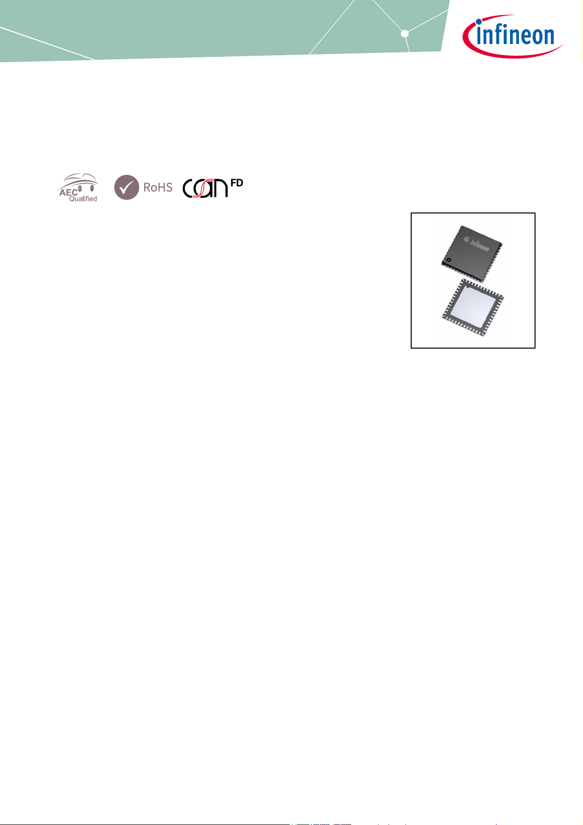
TLE9272QXV33
High-End System Basis Chip Family
1 Overview
Features
Key Features
• Very low quiescent current consumption in SBC Stop and Sleep Mode
• Periodic Cyclic Wake in SBC Normal and Stop Mode
• SMPS 750mA (DC/DC buck) voltage regulator 3.3V to supply high current load with high efficiency
• DC/DC Boost converter for low battery supply voltage
• Low-Drop Voltage Regulator 5V/100mA, protected for off-board usage
• High-Speed CAN Transceiver:
– fully compliant to ISO11898-2:2016
– supporting CAN FD communication up to 5Mbps
• Up to 3 LIN Transceivers LIN2.2, SAE J2602 with programmable TXD timeout feature and LIN Flash Mode
• Compliant with “Hardware Requirements for LIN, CAN and FlexRay Interfaces in Automotive Applications”
Revision 1.3, 2012-05-04
• One universal High-Voltage Wake Input for voltage level monitoring
• Configurable wake-up sources
• Reset Output
• Configurable timeout and window watchdog
• Fail-Safe Input to monitor MCU hardware functionality
• Up to three Fail-Safe Outputs (depending on configurations) to activate external loads in case of system
malfunctions are detected
• Overtemperature and short circuit protection feature
• Wide input voltage and temperature range
•Software compatible with latest Infineon SBC families
• Green Product (RoHS compliant) & AEC Qualified
• PG-VQFN-48-31 leadless exposed-pad power package with Lead Tip Inspection (LTI)
Scalable System Basis Chip (SBC) Family
• Product family with various products for complete scalable application coverage
• Dedicated Datasheets are available for the different product variants
Page 2
TLE9272QXV33
Overview
• Complete compatibility (hardware and software) across the family
• TLE9273 with 4 LIN transceivers, SMPS Boost with 2 output voltage configurations
• TLE9272 with 3 LIN transceivers, SMPS Boost with 2 output voltage configurations
• TLE9271 with 2 LIN transceivers, SMPS Boost with 2 output voltage configurations
• Product variants for 5V (TLE927xQX) and 3.3V (TLE927xQXV33) output voltage for main voltage regulator
Potential applications
•Body control modules
•Gateway
• HVAC ECU and Control panel
Product validation
Qualified for automotive applications. Product validation according to AEC-Q100/101.
Description
The TLE9272QXV33 is a monolithic integrated circuit in an exposed pad PG-VQFN-48-31 (7mm x 7mm) leadless
package with Lead Tip Inspection (LTI) feature supporting Automatic Optical Inspection (AOI).
The device is designed for various CAN-LIN automotive applications as the main supply for the microcontroller
and as the interface for LIN and CAN bus networks.
The System Basis Chip (SBC) provides the main functions for supporting these applications, such as a Switch
Mode Power Supply regulator (SMPS) for on-board 3.3V supply, another 5V low-dropout voltage regulator with
off-board protection, e.g. sensor supply, a DC/DC Boost converter for low supply voltage, an HS-CAN
transceiver supporting CAN FD, a LIN transceiver for data transmission and a 16-bit Serial Peripheral Interface
(SPI) to control and monitor the device. Additional feature include a timeout / window watchdog circuit with
a reset feature, Fail-Safe Input and Fail-Safe Outputs and undervoltage reset features.
The device offers low-power modes in order to minimize current consumption on applications that are
connected permanently to the battery. A wake-up from the low-power mode is possible via a message on the
buses, via the bi-level sensitive monitoring/wake-up input as well as via cyclic wake.
The device is designed to withstand the severe conditions of automotive applications.
Type Package Marking
TLE9272QXV33 PG-VQFN-48-31 TLE9272QXV33
Datasheet 2 Rev. 1.5
2019-09-27
Page 3

TLE9272QXV33
Table of Contents
1 Overview . . . . . . . . . . . . . . . . . . . . . . . . . . . . . . . . . . . . . . . . . . . . . . . . . . . . . . . . . . . . . . . . . . . . . . . . 1
Features . . . . . . . . . . . . . . . . . . . . . . . . . . . . . . . . . . . . . . . . . . . . . . . . . . . . . . . . . . . . . . . . . . . . . . . . 1
Potential applications . . . . . . . . . . . . . . . . . . . . . . . . . . . . . . . . . . . . . . . . . . . . . . . . . . . . . . . . . . . . . 2
Product validation . . . . . . . . . . . . . . . . . . . . . . . . . . . . . . . . . . . . . . . . . . . . . . . . . . . . . . . . . . . . . . . . 2
Description . . . . . . . . . . . . . . . . . . . . . . . . . . . . . . . . . . . . . . . . . . . . . . . . . . . . . . . . . . . . . . . . . . . . . . 2
Table of Contents . . . . . . . . . . . . . . . . . . . . . . . . . . . . . . . . . . . . . . . . . . . . . . . . . . . . . . . . . . . . . . . . . 3
2 Block Diagram . . . . . . . . . . . . . . . . . . . . . . . . . . . . . . . . . . . . . . . . . . . . . . . . . . . . . . . . . . . . . . . . . . . 6
3 Pin Configuration . . . . . . . . . . . . . . . . . . . . . . . . . . . . . . . . . . . . . . . . . . . . . . . . . . . . . . . . . . . . . . . . . 7
3.1 Pin Assignment . . . . . . . . . . . . . . . . . . . . . . . . . . . . . . . . . . . . . . . . . . . . . . . . . . . . . . . . . . . . . . . . . . . . . . . . . . . 7
3.2 Pin Definitions and Functions . . . . . . . . . . . . . . . . . . . . . . . . . . . . . . . . . . . . . . . . . . . . . . . . . . . . . . . . . . . . . . 8
3.3 Hints for Unused Pins . . . . . . . . . . . . . . . . . . . . . . . . . . . . . . . . . . . . . . . . . . . . . . . . . . . . . . . . . . . . . . . . . . . . 10
4 General Product Characteristics . . . . . . . . . . . . . . . . . . . . . . . . . . . . . . . . . . . . . . . . . . . . . . . . . . . 11
4.1 Absolute Maximum Ratings . . . . . . . . . . . . . . . . . . . . . . . . . . . . . . . . . . . . . . . . . . . . . . . . . . . . . . . . . . . . . . . 11
4.2 Functional Range . . . . . . . . . . . . . . . . . . . . . . . . . . . . . . . . . . . . . . . . . . . . . . . . . . . . . . . . . . . . . . . . . . . . . . . . 13
4.3 Thermal Resistance . . . . . . . . . . . . . . . . . . . . . . . . . . . . . . . . . . . . . . . . . . . . . . . . . . . . . . . . . . . . . . . . . . . . . . 14
4.4 Current Consumption . . . . . . . . . . . . . . . . . . . . . . . . . . . . . . . . . . . . . . . . . . . . . . . . . . . . . . . . . . . . . . . . . . . . 15
5 System Features . . . . . . . . . . . . . . . . . . . . . . . . . . . . . . . . . . . . . . . . . . . . . . . . . . . . . . . . . . . . . . . . 18
5.1 State Machine Description and SBC Mode Control . . . . . . . . . . . . . . . . . . . . . . . . . . . . . . . . . . . . . . . . . . 18
5.1.1 SBC Init Mode and Device Configuration . . . . . . . . . . . . . . . . . . . . . . . . . . . . . . . . . . . . . . . . . . . . . . . . . 19
5.1.2 SBC Normal Mode . . . . . . . . . . . . . . . . . . . . . . . . . . . . . . . . . . . . . . . . . . . . . . . . . . . . . . . . . . . . . . . . . . . . . . 21
5.1.3 SBC Stop Mode . . . . . . . . . . . . . . . . . . . . . . . . . . . . . . . . . . . . . . . . . . . . . . . . . . . . . . . . . . . . . . . . . . . . . . . . 21
5.1.4 SBC Sleep Mode . . . . . . . . . . . . . . . . . . . . . . . . . . . . . . . . . . . . . . . . . . . . . . . . . . . . . . . . . . . . . . . . . . . . . . . 22
5.1.5 SBC Restart Mode . . . . . . . . . . . . . . . . . . . . . . . . . . . . . . . . . . . . . . . . . . . . . . . . . . . . . . . . . . . . . . . . . . . . . . 23
5.1.6 SBC Fail-Safe Mode . . . . . . . . . . . . . . . . . . . . . . . . . . . . . . . . . . . . . . . . . . . . . . . . . . . . . . . . . . . . . . . . . . . . 24
5.1.7 SBC Development Mode . . . . . . . . . . . . . . . . . . . . . . . . . . . . . . . . . . . . . . . . . . . . . . . . . . . . . . . . . . . . . . . . 25
5.2 Wake Features . . . . . . . . . . . . . . . . . . . . . . . . . . . . . . . . . . . . . . . . . . . . . . . . . . . . . . . . . . . . . . . . . . . . . . . . . . 26
5.2.1 Cyclic Wake . . . . . . . . . . . . . . . . . . . . . . . . . . . . . . . . . . . . . . . . . . . . . . . . . . . . . . . . . . . . . . . . . . . . . . . . . . . 26
5.2.2 Internal Timer . . . . . . . . . . . . . . . . . . . . . . . . . . . . . . . . . . . . . . . . . . . . . . . . . . . . . . . . . . . . . . . . . . . . . . . . . 27
5.3 Supervision Features . . . . . . . . . . . . . . . . . . . . . . . . . . . . . . . . . . . . . . . . . . . . . . . . . . . . . . . . . . . . . . . . . . . . . 27
6 DC/DC Regulator . . . . . . . . . . . . . . . . . . . . . . . . . . . . . . . . . . . . . . . . . . . . . . . . . . . . . . . . . . . . . . . . 28
6.1 Block Description . . . . . . . . . . . . . . . . . . . . . . . . . . . . . . . . . . . . . . . . . . . . . . . . . . . . . . . . . . . . . . . . . . . . . . . . 28
6.2 Functional Description Buck converter . . . . . . . . . . . . . . . . . . . . . . . . . . . . . . . . . . . . . . . . . . . . . . . . . . . . 29
6.2.1 Startup Procedure (Soft Start) . . . . . . . . . . . . . . . . . . . . . . . . . . . . . . . . . . . . . . . . . . . . . . . . . . . . . . . . . . . 30
6.2.2 Buck regulator Status register . . . . . . . . . . . . . . . . . . . . . . . . . . . . . . . . . . . . . . . . . . . . . . . . . . . . . . . . . . . 30
6.2.3 External components . . . . . . . . . . . . . . . . . . . . . . . . . . . . . . . . . . . . . . . . . . . . . . . . . . . . . . . . . . . . . . . . . . 31
6.3 Functional Description Boost . . . . . . . . . . . . . . . . . . . . . . . . . . . . . . . . . . . . . . . . . . . . . . . . . . . . . . . . . . . . . 32
6.3.1 Boost Regulator Status register . . . . . . . . . . . . . . . . . . . . . . . . . . . . . . . . . . . . . . . . . . . . . . . . . . . . . . . . . 33
6.3.2 External Components . . . . . . . . . . . . . . . . . . . . . . . . . . . . . . . . . . . . . . . . . . . . . . . . . . . . . . . . . . . . . . . . . . 33
6.3.2.1 Peak Overcurrent Detection . . . . . . . . . . . . . . . . . . . . . . . . . . . . . . . . . . . . . . . . . . . . . . . . . . . . . . . . . . 33
6.4 Power Scenarios . . . . . . . . . . . . . . . . . . . . . . . . . . . . . . . . . . . . . . . . . . . . . . . . . . . . . . . . . . . . . . . . . . . . . . . . . 34
6.4.1 Buck and Boost in SBC Normal Mode . . . . . . . . . . . . . . . . . . . . . . . . . . . . . . . . . . . . . . . . . . . . . . . . . . . . 34
6.4.2 Buck and Boost in SBC Stop Mode Operation . . . . . . . . . . . . . . . . . . . . . . . . . . . . . . . . . . . . . . . . . . . . . 34
6.4.2.1 Automatic Transition from PFM to PWM in SBC Stop Mode . . . . . . . . . . . . . . . . . . . . . . . . . . . . . . . 34
Datasheet 3 Rev. 1.5
2019-09-27
Page 4

TLE9272QXV33
6.4.2.2 Manual Transition from PFM to PWM in SBC Stop Mode . . . . . . . . . . . . . . . . . . . . . . . . . . . . . . . . . . 35
6.4.2.3 SBC Stop to Normal Mode Transition . . . . . . . . . . . . . . . . . . . . . . . . . . . . . . . . . . . . . . . . . . . . . . . . . . 36
6.4.3 Buck and Boost in SBC Sleep and Fail Safe Mode . . . . . . . . . . . . . . . . . . . . . . . . . . . . . . . . . . . . . . . . . . 36
6.4.3.1 SBC Sleep/Fail Safe Mode to Normal Mode Transition . . . . . . . . . . . . . . . . . . . . . . . . . . . . . . . . . . . 36
6.5 Electrical Characteristics . . . . . . . . . . . . . . . . . . . . . . . . . . . . . . . . . . . . . . . . . . . . . . . . . . . . . . . . . . . . . . . . . 37
7 Voltage Regulator 2 . . . . . . . . . . . . . . . . . . . . . . . . . . . . . . . . . . . . . . . . . . . . . . . . . . . . . . . . . . . . . . 40
7.1 Block Description . . . . . . . . . . . . . . . . . . . . . . . . . . . . . . . . . . . . . . . . . . . . . . . . . . . . . . . . . . . . . . . . . . . . . . . . 40
7.2 Functional Description . . . . . . . . . . . . . . . . . . . . . . . . . . . . . . . . . . . . . . . . . . . . . . . . . . . . . . . . . . . . . . . . . . . 41
7.3 Electrical Characteristics . . . . . . . . . . . . . . . . . . . . . . . . . . . . . . . . . . . . . . . . . . . . . . . . . . . . . . . . . . . . . . . . . 42
8 High Speed CAN Transceiver . . . . . . . . . . . . . . . . . . . . . . . . . . . . . . . . . . . . . . . . . . . . . . . . . . . . . . 44
8.1 Block Description . . . . . . . . . . . . . . . . . . . . . . . . . . . . . . . . . . . . . . . . . . . . . . . . . . . . . . . . . . . . . . . . . . . . . . . . 44
8.2 Functional Description . . . . . . . . . . . . . . . . . . . . . . . . . . . . . . . . . . . . . . . . . . . . . . . . . . . . . . . . . . . . . . . . . . . 44
8.2.1 CAN OFF Mode . . . . . . . . . . . . . . . . . . . . . . . . . . . . . . . . . . . . . . . . . . . . . . . . . . . . . . . . . . . . . . . . . . . . . . . . . 46
8.2.2 CAN Normal Mode . . . . . . . . . . . . . . . . . . . . . . . . . . . . . . . . . . . . . . . . . . . . . . . . . . . . . . . . . . . . . . . . . . . . . 46
8.2.3 CAN Receive Only Mode . . . . . . . . . . . . . . . . . . . . . . . . . . . . . . . . . . . . . . . . . . . . . . . . . . . . . . . . . . . . . . . . 47
8.2.4 CAN Wake Capable Mode (Wake-up Pattern) . . . . . . . . . . . . . . . . . . . . . . . . . . . . . . . . . . . . . . . . . . . . . . 47
8.2.5 TXDCAN Time-out Feature . . . . . . . . . . . . . . . . . . . . . . . . . . . . . . . . . . . . . . . . . . . . . . . . . . . . . . . . . . . . . . 48
8.2.6 Bus Dominant Clamping . . . . . . . . . . . . . . . . . . . . . . . . . . . . . . . . . . . . . . . . . . . . . . . . . . . . . . . . . . . . . . . . 49
8.2.7 VCAN Undervoltage Detection . . . . . . . . . . . . . . . . . . . . . . . . . . . . . . . . . . . . . . . . . . . . . . . . . . . . . . . . . . . 49
8.3 Electrical Characteristics . . . . . . . . . . . . . . . . . . . . . . . . . . . . . . . . . . . . . . . . . . . . . . . . . . . . . . . . . . . . . . . . . 50
9 LIN Transceiver . . . . . . . . . . . . . . . . . . . . . . . . . . . . . . . . . . . . . . . . . . . . . . . . . . . . . . . . . . . . . . . . . 58
9.1 Block Description . . . . . . . . . . . . . . . . . . . . . . . . . . . . . . . . . . . . . . . . . . . . . . . . . . . . . . . . . . . . . . . . . . . . . . . . 58
9.1.1 LIN Specifications . . . . . . . . . . . . . . . . . . . . . . . . . . . . . . . . . . . . . . . . . . . . . . . . . . . . . . . . . . . . . . . . . . . . . . 58
9.2 Functional Description . . . . . . . . . . . . . . . . . . . . . . . . . . . . . . . . . . . . . . . . . . . . . . . . . . . . . . . . . . . . . . . . . . . 59
9.2.1 LIN OFF Mode . . . . . . . . . . . . . . . . . . . . . . . . . . . . . . . . . . . . . . . . . . . . . . . . . . . . . . . . . . . . . . . . . . . . . . . . . . 59
9.2.2 LIN Normal Mode . . . . . . . . . . . . . . . . . . . . . . . . . . . . . . . . . . . . . . . . . . . . . . . . . . . . . . . . . . . . . . . . . . . . . . 60
9.2.3 LIN Receive Only Mode . . . . . . . . . . . . . . . . . . . . . . . . . . . . . . . . . . . . . . . . . . . . . . . . . . . . . . . . . . . . . . . . . 60
9.2.4 LIN Wake Capable Mode . . . . . . . . . . . . . . . . . . . . . . . . . . . . . . . . . . . . . . . . . . . . . . . . . . . . . . . . . . . . . . . . 60
9.2.5 TXDLIN Time-Out Feature . . . . . . . . . . . . . . . . . . . . . . . . . . . . . . . . . . . . . . . . . . . . . . . . . . . . . . . . . . . . . . . 61
9.2.6 Bus Dominant Clamping . . . . . . . . . . . . . . . . . . . . . . . . . . . . . . . . . . . . . . . . . . . . . . . . . . . . . . . . . . . . . . . . 62
9.2.7 Undervoltage Detection . . . . . . . . . . . . . . . . . . . . . . . . . . . . . . . . . . . . . . . . . . . . . . . . . . . . . . . . . . . . . . . . 62
9.2.8 Slope Selection . . . . . . . . . . . . . . . . . . . . . . . . . . . . . . . . . . . . . . . . . . . . . . . . . . . . . . . . . . . . . . . . . . . . . . . . 62
9.2.9 Flash Programming via LIN . . . . . . . . . . . . . . . . . . . . . . . . . . . . . . . . . . . . . . . . . . . . . . . . . . . . . . . . . . . . . 63
9.3 Electrical Characteristics of the LIN Transceiver . . . . . . . . . . . . . . . . . . . . . . . . . . . . . . . . . . . . . . . . . . . . 64
10 Wake Input . . . . . . . . . . . . . . . . . . . . . . . . . . . . . . . . . . . . . . . . . . . . . . . . . . . . . . . . . . . . . . . . . . . . . 69
10.1 Block Description . . . . . . . . . . . . . . . . . . . . . . . . . . . . . . . . . . . . . . . . . . . . . . . . . . . . . . . . . . . . . . . . . . . . . . . . 69
10.2 Functional Description . . . . . . . . . . . . . . . . . . . . . . . . . . . . . . . . . . . . . . . . . . . . . . . . . . . . . . . . . . . . . . . . . . . 70
10.2.1 Wake Input Configuration . . . . . . . . . . . . . . . . . . . . . . . . . . . . . . . . . . . . . . . . . . . . . . . . . . . . . . . . . . . . . . . 71
10.3 Electrical Characteristics . . . . . . . . . . . . . . . . . . . . . . . . . . . . . . . . . . . . . . . . . . . . . . . . . . . . . . . . . . . . . . . . . 72
11 Interrupt Function . . . . . . . . . . . . . . . . . . . . . . . . . . . . . . . . . . . . . . . . . . . . . . . . . . . . . . . . . . . . . . . 73
11.1 Block and Functional Description . . . . . . . . . . . . . . . . . . . . . . . . . . . . . . . . . . . . . . . . . . . . . . . . . . . . . . . . . 73
11.2 Electrical Characteristics . . . . . . . . . . . . . . . . . . . . . . . . . . . . . . . . . . . . . . . . . . . . . . . . . . . . . . . . . . . . . . . . . 75
12 Fail-Safe Outputs and Fail-Safe Input . . . . . . . . . . . . . . . . . . . . . . . . . . . . . . . . . . . . . . . . . . . . . . . 76
12.1 Functional Description . . . . . . . . . . . . . . . . . . . . . . . . . . . . . . . . . . . . . . . . . . . . . . . . . . . . . . . . . . . . . . . . . . . 76
12.2 Fail-Safe Input . . . . . . . . . . . . . . . . . . . . . . . . . . . . . . . . . . . . . . . . . . . . . . . . . . . . . . . . . . . . . . . . . . . . . . . . . . . 77
Datasheet 4 Rev. 1.5
2019-09-27
Page 5

TLE9272QXV33
12.3 Electrical Characteristics . . . . . . . . . . . . . . . . . . . . . . . . . . . . . . . . . . . . . . . . . . . . . . . . . . . . . . . . . . . . . . . . . 78
13 Supervision Functions . . . . . . . . . . . . . . . . . . . . . . . . . . . . . . . . . . . . . . . . . . . . . . . . . . . . . . . . . . . 79
13.1 Reset Function . . . . . . . . . . . . . . . . . . . . . . . . . . . . . . . . . . . . . . . . . . . . . . . . . . . . . . . . . . . . . . . . . . . . . . . . . . 79
13.1.1 Reset Output Description . . . . . . . . . . . . . . . . . . . . . . . . . . . . . . . . . . . . . . . . . . . . . . . . . . . . . . . . . . . . . . . 79
13.1.2 Reset Clamp to high . . . . . . . . . . . . . . . . . . . . . . . . . . . . . . . . . . . . . . . . . . . . . . . . . . . . . . . . . . . . . . . . . . . . 80
13.1.3 Soft Reset Description . . . . . . . . . . . . . . . . . . . . . . . . . . . . . . . . . . . . . . . . . . . . . . . . . . . . . . . . . . . . . . . . . . 80
13.2 Watchdog Function . . . . . . . . . . . . . . . . . . . . . . . . . . . . . . . . . . . . . . . . . . . . . . . . . . . . . . . . . . . . . . . . . . . . . . 81
13.2.1 Time-Out Watchdog . . . . . . . . . . . . . . . . . . . . . . . . . . . . . . . . . . . . . . . . . . . . . . . . . . . . . . . . . . . . . . . . . . . . 82
13.2.2 Window Watchdog . . . . . . . . . . . . . . . . . . . . . . . . . . . . . . . . . . . . . . . . . . . . . . . . . . . . . . . . . . . . . . . . . . . . . 82
13.2.3 Watchdog Setting Check Sum . . . . . . . . . . . . . . . . . . . . . . . . . . . . . . . . . . . . . . . . . . . . . . . . . . . . . . . . . . . 83
13.2.4 Watchdog during SBC Stop Mode . . . . . . . . . . . . . . . . . . . . . . . . . . . . . . . . . . . . . . . . . . . . . . . . . . . . . . . . 83
13.2.4.1 WD Start in SBC Stop Mode due to BUS Wake . . . . . . . . . . . . . . . . . . . . . . . . . . . . . . . . . . . . . . . . . . . 84
13.3 VS Power ON Reset . . . . . . . . . . . . . . . . . . . . . . . . . . . . . . . . . . . . . . . . . . . . . . . . . . . . . . . . . . . . . . . . . . . . . . 86
13.4 Under Voltage VLIN . . . . . . . . . . . . . . . . . . . . . . . . . . . . . . . . . . . . . . . . . . . . . . . . . . . . . . . . . . . . . . . . . . . . . . 86
13.5 Buck Regulator Monitoring Features . . . . . . . . . . . . . . . . . . . . . . . . . . . . . . . . . . . . . . . . . . . . . . . . . . . . . . . 87
13.5.1 VCC1 Under Voltage . . . . . . . . . . . . . . . . . . . . . . . . . . . . . . . . . . . . . . . . . . . . . . . . . . . . . . . . . . . . . . . . . . . . 87
13.5.2 VCC1 Overvoltage . . . . . . . . . . . . . . . . . . . . . . . . . . . . . . . . . . . . . . . . . . . . . . . . . . . . . . . . . . . . . . . . . . . . . . 87
13.5.3 VCC1 Short Circuit . . . . . . . . . . . . . . . . . . . . . . . . . . . . . . . . . . . . . . . . . . . . . . . . . . . . . . . . . . . . . . . . . . . . . 88
13.5.4 SMPS Status register . . . . . . . . . . . . . . . . . . . . . . . . . . . . . . . . . . . . . . . . . . . . . . . . . . . . . . . . . . . . . . . . . . . 88
13.6 VCC2 Undervoltage . . . . . . . . . . . . . . . . . . . . . . . . . . . . . . . . . . . . . . . . . . . . . . . . . . . . . . . . . . . . . . . . . . . . . . 88
13.7 VCAN Undervoltage . . . . . . . . . . . . . . . . . . . . . . . . . . . . . . . . . . . . . . . . . . . . . . . . . . . . . . . . . . . . . . . . . . . . . 88
13.8 Thermal Protection . . . . . . . . . . . . . . . . . . . . . . . . . . . . . . . . . . . . . . . . . . . . . . . . . . . . . . . . . . . . . . . . . . . . . . 89
13.8.1 Individual Thermal Shutdown . . . . . . . . . . . . . . . . . . . . . . . . . . . . . . . . . . . . . . . . . . . . . . . . . . . . . . . . . . . 89
13.8.2 Temperature Prewarning . . . . . . . . . . . . . . . . . . . . . . . . . . . . . . . . . . . . . . . . . . . . . . . . . . . . . . . . . . . . . . . 89
13.8.3 SBC Thermal Shutdown . . . . . . . . . . . . . . . . . . . . . . . . . . . . . . . . . . . . . . . . . . . . . . . . . . . . . . . . . . . . . . . . 89
13.9 Electrical Characteristics . . . . . . . . . . . . . . . . . . . . . . . . . . . . . . . . . . . . . . . . . . . . . . . . . . . . . . . . . . . . . . . . . 90
14 Serial Peripheral Interface . . . . . . . . . . . . . . . . . . . . . . . . . . . . . . . . . . . . . . . . . . . . . . . . . . . . . . . . 92
14.1 SPI Description . . . . . . . . . . . . . . . . . . . . . . . . . . . . . . . . . . . . . . . . . . . . . . . . . . . . . . . . . . . . . . . . . . . . . . . . . . 92
14.2 Failure Signalization in the SPI Data Output . . . . . . . . . . . . . . . . . . . . . . . . . . . . . . . . . . . . . . . . . . . . . . . . 93
14.3 SPI Programming . . . . . . . . . . . . . . . . . . . . . . . . . . . . . . . . . . . . . . . . . . . . . . . . . . . . . . . . . . . . . . . . . . . . . . . . 93
14.4 SPI Bit Mapping . . . . . . . . . . . . . . . . . . . . . . . . . . . . . . . . . . . . . . . . . . . . . . . . . . . . . . . . . . . . . . . . . . . . . . . . . 95
14.5 SPI Control Registers . . . . . . . . . . . . . . . . . . . . . . . . . . . . . . . . . . . . . . . . . . . . . . . . . . . . . . . . . . . . . . . . . . . . . 97
14.6 SPI Status Information Registers . . . . . . . . . . . . . . . . . . . . . . . . . . . . . . . . . . . . . . . . . . . . . . . . . . . . . . . . . 105
14.7 Electrical Characteristics . . . . . . . . . . . . . . . . . . . . . . . . . . . . . . . . . . . . . . . . . . . . . . . . . . . . . . . . . . . . . . . . 113
15 Application Information . . . . . . . . . . . . . . . . . . . . . . . . . . . . . . . . . . . . . . . . . . . . . . . . . . . . . . . . . 115
15.1 Application Diagram with Boost Module . . . . . . . . . . . . . . . . . . . . . . . . . . . . . . . . . . . . . . . . . . . . . . . . . . 115
15.2 Application Diagram without Boost Module . . . . . . . . . . . . . . . . . . . . . . . . . . . . . . . . . . . . . . . . . . . . . . . 118
15.3 ESD Tests . . . . . . . . . . . . . . . . . . . . . . . . . . . . . . . . . . . . . . . . . . . . . . . . . . . . . . . . . . . . . . . . . . . . . . . . . . . . . . 121
15.4 Thermal Behavior of Package . . . . . . . . . . . . . . . . . . . . . . . . . . . . . . . . . . . . . . . . . . . . . . . . . . . . . . . . . . . . 122
16 Package Outlines . . . . . . . . . . . . . . . . . . . . . . . . . . . . . . . . . . . . . . . . . . . . . . . . . . . . . . . . . . . . . . . 123
17 Revision History . . . . . . . . . . . . . . . . . . . . . . . . . . . . . . . . . . . . . . . . . . . . . . . . . . . . . . . . . . . . . . . . 124
Datasheet 5 Rev. 1.5
2019-09-27
Page 6

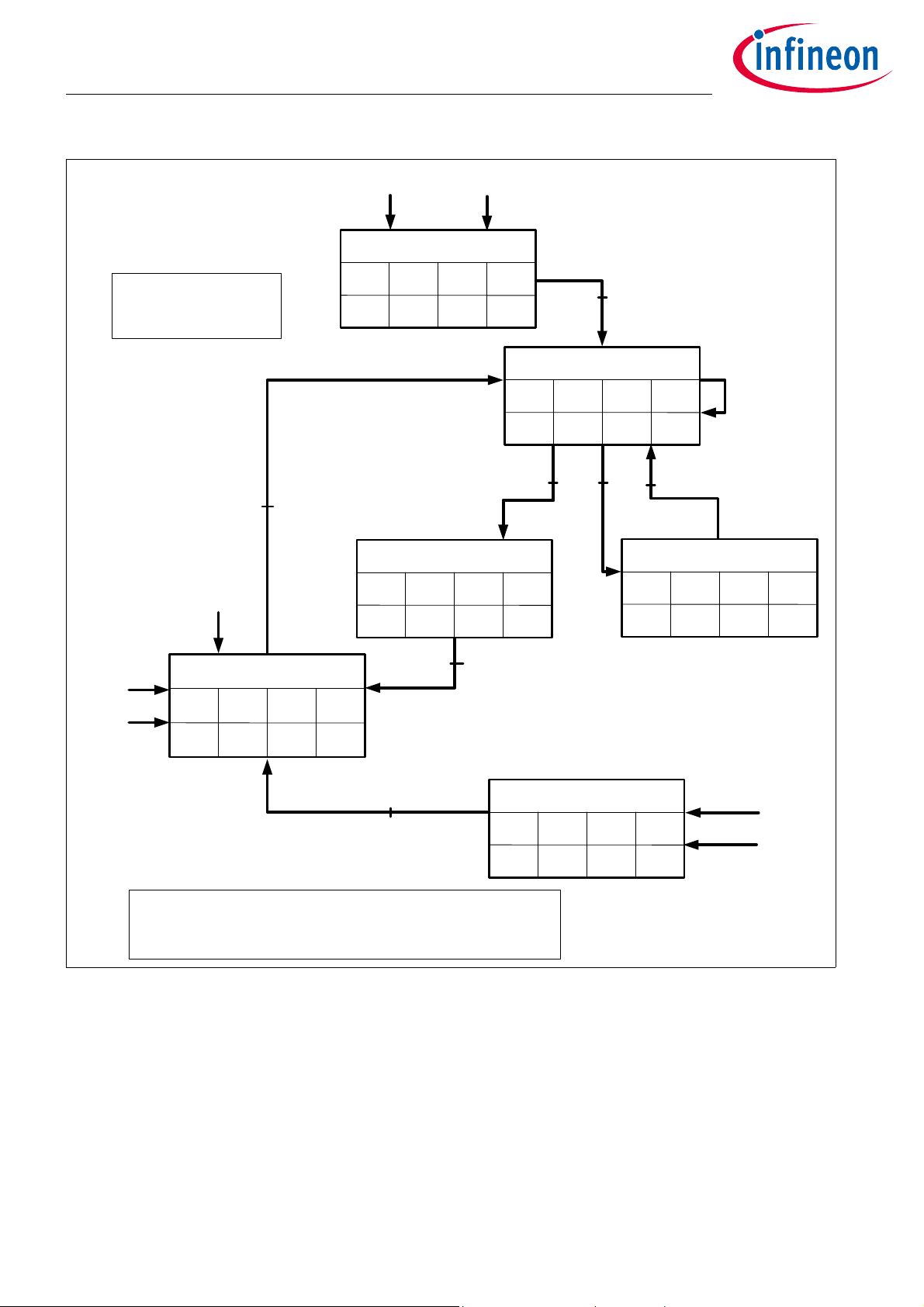
V
CC1
Buck
V
CC2
SPI
Interrupt
Control
SBC
STATE
MACHINE
SDI
SDO
CLK
CSN
BCKSW
VCC2
CAN cell
LIN cell 1
Window Watchdog
WK
TXDLIN
RXDLIN
TXDCAN
RXDCAN
VCAN
CANH
CANL
WK1
RESET
GENERATOR
INT
WAKE
REGISTER
V
s
Vint.
Fail Safe
RO
FO1
LIN cell 2
TXDLIN
RXDLIN
LIN cell 3
TXDLIN
RXDLIN
GND
VCC1
Boost
BSTD
BSTG
SNSP
SNSN
3
3
3
CFG
VLIN
VS2
VSENSE
FO2/FSI
FO3/TEST
VS
LIN1
LIN2
LIN3
TLE9272QXV33
Block Diagram
2 Block Diagram
Figure 1 Block Diagram
Datasheet 6 Rev. 1.5
2019-09-27
Page 7

1 LIN1
2 GND
3 LIN2
4 n.c.
5 LIN3
6 GND
7 n.c.
8 GND
9 CANH
10 CANL
11 GND
12 TXDLIN1
FO3/TEST 48
FO2/FSI 47
FO1 46
VLIN 45
VS2 44
VCC2 43
GND 42
CLK 41
SDI 40
SDO 39
CSN 38
CFG 37
13 RXDLIN1
14 TXDLIN2
15 RXDLIN2
16 TXDLIN3
17 RXDLIN3
18 N.U.
19 N.U.
20 VCAN
21 TXDCAN
22 RXDCAN
23 VCC1
24 RO
25 INT
26 GND
27 BCKSW
28 VS
29 VS
30 VSENSE
31 n.c.
32 SNSN
33 SNSP
34 BSTG
35 BSTD
36 WK
TLE9272QXV33
PG-VQFN-48
TLE9272QXV33
Pin Configuration
3 Pin Configuration
3.1 Pin Assignment
Figure 2 Pin Configuration
Datasheet 7 Rev. 1.5
2019-09-27
Page 8

TLE9272QXV33
Pin Configuration
3.2 Pin Definitions and Functions
Pin Symbol Function
1LIN1 LIN Bus 1. Bus line for the LIN interface, according to ISO. 9141 and LIN
specification 2.1 as well as SAE J2602-2.
2GND Ground: LIN1 and LIN2 common ground.
3LIN2 LIN Bus 2. Bus line for the LIN interface, according to ISO. 9141 and LIN
specification 2.1 as well as SAE J2602-2.
4n.c. not connected. Not bonded internally
5LIN3 LIN Bus 3. Bus line for the LIN interface, according to ISO. 9141 and LIN
specification 2.1 as well as SAE J2602-2.
6GND Ground. LIN3 and LIN4 common ground.
7n.c. not connected. Not bonded internally
8GND Ground.
9CANH CAN High Bus Pin.
10 CANL CAN Low Bus Pin.
11 GND Ground. CAN common ground.
12 TXDLIN1 Transmit LIN1.
13 RXDLIN1 Receive LIN1.
14 TXDLIN2 Transmit LIN2.
15 RXDLIN2 Receive LIN2.
16 TXDLIN3 Transmit LIN3.
17 RXDLIN3 Receive LIN3.
18 N.U. Not Used. Used for internal testing purpose. Do not connect, leave open.
19 N.U. Not Used. Used for internal testing purpose. Do not connect, leave open.
20 VCAN Supply Input for internal HS-CAN module.
21 TXDCAN Transmit CAN.
22 RXDCAN Receive CAN.
23 VCC1 Buck Regulator. Input feedback for Buck regulator
24 RO Reset Output. Active LOW, internal pull-up
25 INT Interrupt Output. Active LOW output
26 GND Ground. Buck regulator ground
27 BCKSW Buck regulator switch node output.
28 VS Buck Supply Voltage. Connected to battery voltage or Boost output voltage
with reverse protection diode. Use a filter against EMC in case the Boost is not
used.
29 VS Buck Supply Voltage. Connected to battery voltage or Boost output voltage
with reverse protection diode. Use a filter against EMC in case the Boost is not
used.
Datasheet 8 Rev. 1.5
2019-09-27
Page 9

TLE9272QXV33
Pin Configuration
Pin Symbol Function
30 VSENSE Sense Input Voltage for Boost.
Boost regulator feedback input. Connect with VS.
31 n.c. not connected. Not bonded internally
32 SNSN Ground. Boost regulator ground.
33 SNSP Boost Transistor Source. Source connection for external MOSFET, sense
resistor connection. Connect to GND if Boost regulator is not used.
34 BSTG Boost Transistor Gate. Gate connection for external MOSFET. Connect to GND
or leave open if Boost regulator is not used.
35 BSTD Boost Transistor Drain. Drain connection for external MOSFET. Connect to VS if
Boost regulator is not used.
36 WK Wake Input.
37 CFG Hardware initialization pin.
external pull-up to VCC1 needed. Refer to Chapter 15.
38 CSN SPI Chip Select Not Input.
39 SDO SPI Data Output. Out of SBC (=MISO)
40 SDI SPI Data Input. Into SBC (=MOSI)
41 CLK SPI Clock Input.
42 GND Ground.
43 VCC2 Voltage Regulator Output 2.
44 VS2 Supply Voltage for VCC2. Connected to battery voltage with reverse protection
diode and filter against EMC.
45 VLIN Reference Voltage for LIN. Connected to battery voltage with reverse
protection diode and filter against EMC.
46 FO1 Fail Output 1. active LOW, open drain.
47 FO2/FSI Fail Output 2 - Side Indicator. Side Indicator 1.25Hz 50% duty cycle output;
active LOW, open drain.
FSI. Fail-Safe Input (default configuration); connect to GND if not used.
48 FO3/TEST Fail Output 3 - Pulsed Lighted Output. Break/rear light 100Hz 20% duty cycle
output; active LOW, open-drain.
TEST. Connect to GND to activate SBC Development Mode; integrated pull-up
resistor. Connect to VS with a pull-up resistor or leave open for normal operation.
Coolin
g Tab
1) The exposed die pad at the bottom of the package allows better power dissipation of heat from the SBC via the PCB.
Datasheet 9 Rev. 1.5
GND Cooling Tab - Exposed Die Pad; for cooling purposes, do not use as the only
electrical ground.
The exposed die pad is not connected to any active part of the IC. However it should be connected to GND for the best
EMC performance.
1)
2019-09-27
Page 10

TLE9272QXV33
Pin Configuration
3.3 Hints for Unused Pins
It must be ensured that the correct configurations are also selected, i.e. in case functions are not used that
they are disabled via SPI:
• WK: connected to GND and disable the WK input via SPI;
• LINx, RXDLINx, TXDLINx, RXDCAN, TXDCAN, CANH, CANL: leave all pins open;
• BSTD: connect to VS in case the Boost regulator is not used and keep disabled;
• BSTG: connect to GND or leave open in case the Boost regulator is not used and keep disabled;
• SNSP, SNSN: connect to GND in case the Boost regulator is not used;
•RO / FOx: leave open;
•INT: leave open;
• TEST: connect to GND during power-up to activate SBC Development Mode; connect to VS or leave open
for normal user mode operation;
• VCC2: leave open and keep disabled;
• VCAN: connect to VCC1;
• n.c.: not connected, not bonded internally, connected to GND;
• Unused pins routed to an external connector which leaves the ECU should feature a zero ohm jumper
(depopulated if unused) or ESD protection.
Datasheet 10 Rev. 1.5
2019-09-27
Page 11

TLE9272QXV33
General Product Characteristics
4 General Product Characteristics
4.1 Absolute Maximum Ratings
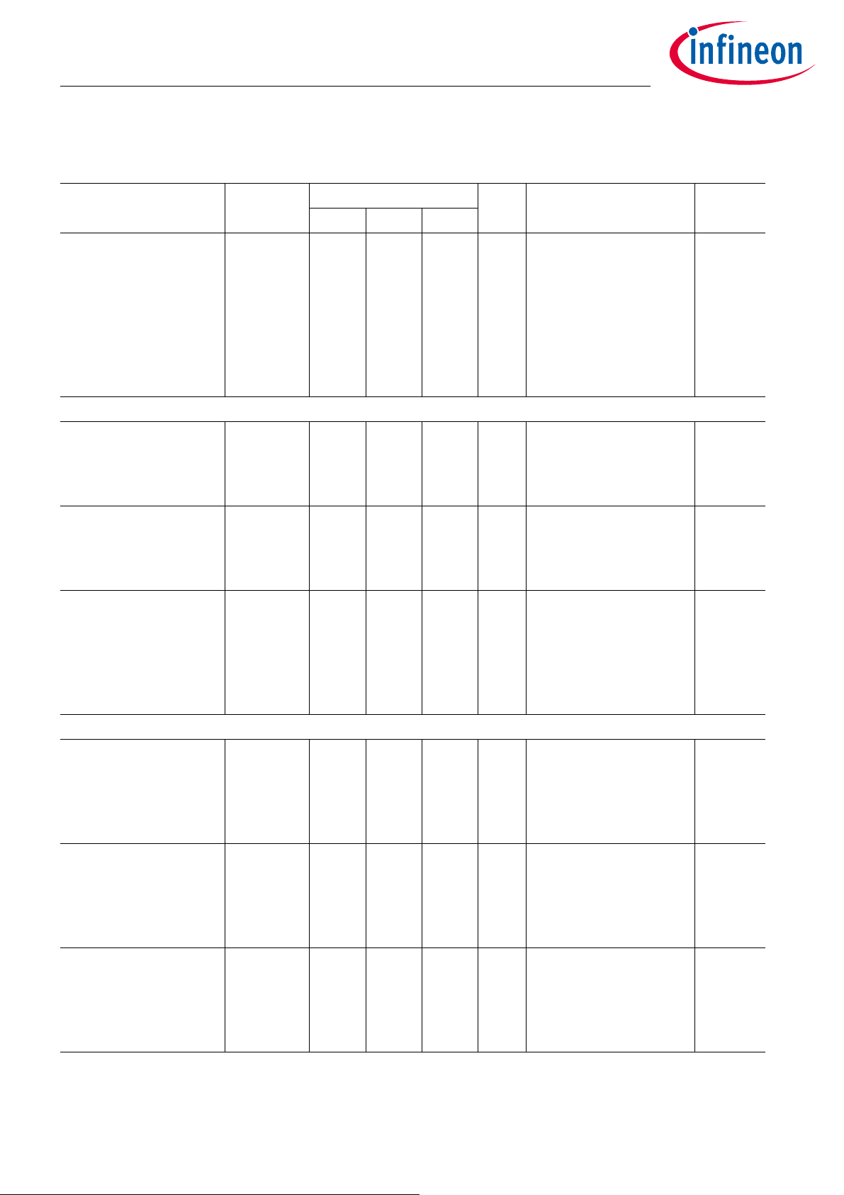
Table 1 Absolute Maximum Ratings
1)
Tj = -40 °C to +150 °C; all voltages with respect to ground, positive current flowing into pin (unless otherwise
specified)
Parameter Symbol Values Unit Note or
Min. Typ. Max.
Test Condition
Number
Voltages
Supply Voltage VS pin V
Supply Voltage VS2 pin V
Supply Voltage VS pin V
S, max
S2, max
S, max
-0.3 – 28 V – P_4.1.1
-0.3 – 28 V – P_4.1.25
-0.3 – 40 V Load Dump,
P_4.1.2
max. 400 ms
Supply Voltage VS2 pin V
S2, max
-0.3 – 40 V Load Dump,
P_4.1.26
max. 400 ms
LIN Supply Voltage VLIN pin V
Boost drain Voltage BSTD
LIN, max
V
BSTD, max
-0.3 – 40 V – P_4.1.12
-0.3 – 28 V – P_4.1.19
pin
Boost drain Voltage BSTD
pin
Boost Gate Voltage BSTG pin V
Supply Voltage SNSP pin V
Sense Voltage VSENSE pin V
Buck switch BCKSW pin V
Buck Regulator feedback,
V
BSTD, max
BSTG, max
SNSP, max
SENSE, max
BCKSW, max
V
CC1, max
-0.3 – 40 V Load Dump,
max. 400 ms
-0.3 – 40 V – P_4.1.21
-0.3 – 40 V – P_4.1.22
-0.3 – 40 V – P_4.1.23
-0.3 – VS+0.3 V – P_4.1.24
-0.3 – 5.5 V – P_4.1.3
P_4.1.20
pin VCC1
Voltage Regulator 2 Output,
V
CC2, max
-0.3 – 40 V – P_4.1.5
pin VCC2
Wake Input V
Fail Pins FO1, FO2/FSI,
WK, max
V
FOx, max
-0.3 – 40 V – P_4.1.6
-0.3 – 40 V – P_4.1.7
FO3/TEST
Configuration Pin CFG V
CFG, max
-0.3 – VCC1
V – P_4.1.8
+ 0.3
LINx, CANH, CANL V
V
=CANH-CANL V
diff
Logic Input Voltage V
BUS, max
DIFF
I, max
-27 – 40 V – P_4.1.9
-5 – 10 V – P_4.1.28
-0.3 – VCC1
V – P_4.1.10
+ 0.3
Datasheet 11 Rev. 1.5
2019-09-27
Page 12

TLE9272QXV33
General Product Characteristics
Table 1 Absolute Maximum Ratings1) (cont’d)
= -40 °C to +150 °C; all voltages with respect to ground, positive current flowing into pin (unless otherwise
T
j
specified)
Parameter Symbol Values Unit Note or
Test Condition
Logic Output Voltage V
O, max
Min. Typ. Max.
-0.3 – VCC1
V – P_4.1.27
Number
+ 0.3
VCAN Input Voltage V
VCAN, max
-0.3 – 5.5 V – P_4.1.11
Temperatures
Junction Temperature T
Storage Temperature T
j
stg
-40 – 150 °C – P_4.1.13
-55 – 150 °C – P_4.1.14
ESD Susceptibility
ESD Resistivity to GND V
ESD Resistivity to GND,
ESD
V
ESD
-2 – 2 kV HBM
-8 – 8 kV HBM
2)
3)2)
P_4.1.15
P_4.1.16
CANH, CANL, LINx
ESD Resistivity to GND V
ESD Resistivity Pin 1,
12,13,24,25,36,37,48 (corner
ESD
V
ESD1,12,13,24,
25,36,37,48
-500 – 500 V CDM
-750 – 750 V CDM
4)
4)
P_4.1.17
P_4.1.18
pins) to GND
1) Not subject to production test, specified by design.
2) ESD susceptibility, “HBM” according to ANSI/ESDA/JEDEC JS-001 (1.5kΩ, 100pF).
3) For ESD GUN Resistivity, tested at 6KV (according to IEC61000-4-2 “gun test” (330Ω, 150pF)), it is shown in Application
Information and test report, provided from IBEE, is available.
4) ESD susceptibility, Charged Device Model “CDM” EIA/JESD22-C101 or ESDA STM5.3.1.
Notes
1. Stresses above the ones listed here may cause permanent damage to the device. Exposure to absolute
maximum rating conditions for extended periods may affect device reliability.
2. Integrated protection functions are designed to prevent IC destruction under fault conditions described in the
data sheet. Fault conditions are considered as “outside” normal operating range. Protection functions are
not designed for continuous repetitive operation.
Datasheet 12 Rev. 1.5
2019-09-27
Page 13
TLE9272QXV33
General Product Characteristics
4.2 Functional Range
Table 2 Functional Range
Parameter Symbol Values Unit Note or
Test Condition
see section
POR
Supply Voltage V
S,func
Min. Typ. Max.
V
POR
–28V1) V
Number
P_4.2.1
Chapter 13.9
LIN Supply Voltage (VLIN
V
REF,LIN
5.5 – 18 V P_4.2.2
pin)
CAN Supply Voltage V
CFG external pull-up R
SPI frequency f
CAN
CFG
SPI
4.75 – 5.25 V – P_4.2.3
10 – 22 kΩ –P_4.2.6
––4MHzsee
P_4.2.4
Chapter 14.7 for
f
SPI,max
Junction Temperature T
1) Including Power-On Reset, Over- and Under voltage Protection
j
-40 – 150 °C – P_4.2.5
Note: Within the functional range the IC operates as described in the circuit description. The electrical
characteristics are specified within the conditions given in the related electrical characteristics table.
Device Behavior Outside of Specified Functional Range:
• 28V < V
< 40V: Device will still be functional; the specified electrical characteristics may not be ensured
S,func
anymore. The Buck and VCC2 will work, however, a thermal shutdown may occur due to high power
dissipation. The specified SPI communication speed is ensured. The absolute maximum ratings are not
violated, however the device is not intended for continuous operation of VS >28V. Operating the device at
high junction temperatures for prolonged periods of time may reduce the life of the device.
• 18V < V
<28V: The LIN transceiver is still functional. However, the communication may fail due to out-of-
LIN
LIN-spec operation;
• V
LIN,UVD
< V
< 5.5V: The LIN transceiver is still functional. However, the communication may fail due to
LIN
out-of-LIN-spec operation;
• V
< 4.75V: The undervoltage bit VCAN_UV will be set in the SPI register BUS_STAT_1 and the transmitter
CAN
will be disabled as long as the UV condition is present;
• 5.25V < V
< 5.50V: CAN transceiver still functional. However, the communication may fail due to out-of-
CAN
spec operation;
• V
< VS < 5.5V: Device will be still functional; the specified electrical characteristics may not be ensured
POR,f
anymore:
– The voltage regulators will enter the low-drop operation mode;
–A VCC1_UV reset could be triggered depending on the Vrtx settings;
– The LIN transmitter will be disabled if V
LIN
< V
is reached and VLIN_UV bit on SUP_STAT is set;
LIN,UVD
– FOx outputs will remain ON if they were enabled;
– The specified SPI communication speed is ensured.
Datasheet 13 Rev. 1.5
2019-09-27
Page 14

TLE9272QXV33
General Product Characteristics
4.3 Thermal Resistance
Table 3 Thermal Resistance
Parameter Symbol Values Unit Note or
Junction to Soldering Point R
Junction to Ambient R
1) Not subject to production test, specified by design.
2) According to Jedec JESD51-2,-5,-7 at natural convection on FR4 2s2p board for 1.5W. Board: 76.2x114.3x1.5mm3 with
2 inner copper layers (35µm thick), with a thermal via array under the exposed pad contacting the first inner copper
layer and 300mm2 cooling area on the bottom layer (70µm). For more details, refer to Chapter 15.4.
1)
thJSP
thJA
Number
Min. Typ. Max.
– 6 – K/W Exposed Pad P_4.3.1
–33–K/W
Test Condition
2)
P_4.3.2
Datasheet 14 Rev. 1.5
2019-09-27
Page 15
TLE9272QXV33
General Product Characteristics
4.4 Current Consumption
Table 4 Current Consumption
Current consumption values are specified at T
= 25°C, VS = 13.5V, all outputs open (unless otherwise specified)
j
Parameter Symbol Values Unit Note or Test Condition Number
Min. Typ. Max.
SBC Normal Mode
Normal Mode current
consumption
I
Normal
– 5 10 mA 5.5V < VS < 28V
no load on VCC1
T
= -40°C to +150°C
j
P_4.4.1
VCC2 / CAN / LIN / BOOST
= OFF
SBC Stop Mode
Stop Mode current
consumption
I
Stop,25
– 5065µA
1)2)
Tj = 25°C
Buck module in PFM
P_4.4.2
no load on VCC1
VCC2 = OFF;
CAN / LINx = OFF
Watchdog = OFF
WK enabled
Stop Mode current
consumption
I
Stop,85
–95–µA
BOOST = OFF
1)2)3)
Tj = 85°C;
Buck module in PFM
P_4.4.3
no load on VCC1
VCC2 = OFF;
CAN / LINx = OFF
Watchdog = OFF
WK enabled
BOOST = OFF
Stop Mode current
consumption, VCC2
enabled
I
Stop,VCC2,25
– 7095µA
1)2)
Tj = 25°C
Buck module in PFM
no load on VCC1
P_4.4.4
VS2 = VS
VCC2 = ON (no load); CAN
/ LINx = OFF
Watchdog = OFF
WK enabled
BOOST = OFF
Datasheet 15 Rev. 1.5
2019-09-27
Page 16
TLE9272QXV33
General Product Characteristics
Table 4 Current Consumption (cont’d)
Current consumption values are specified at T
Parameter Symbol Values Unit Note or Test Condition Number
Min. Typ. Max.
Stop Mode current
I
Stop,C25
– 6585µA
consumption, cyclic
wake
SBC Sleep Mode
= 25°C, VS = 13.5V, all outputs open (unless otherwise specified)
j
1)2)
Tj = 25°C
P_4.4.5
Buck module in PFM
no load on VCC1
VCC2 = OFF;
CAN / LINx = OFF
Watchdog = ON
WK enabled
BOOST = OFF
Sleep Mode current
I
Sleep,25
consumption
Sleep Mode current
I
Sleep,85
consumption
Sleep Mode current
I
Sleep,VCC2,25
consumption, VCC2
enabled
Incremental Current Consumption
Current consumption for
I
CAN,rec
CAN, recessive state
– 3050µA1) Tj = 25°C
VCC1,VCC2 = OFF
CAN / LINx = OFF,
WK enabled
–80–µA
1)3)
Tj = 85°C
VCC1,VCC2 = OFF
CAN / LINx = OFF
WK enabled
– 5075µA1) Tj = 25°C
VCC1= OFF
VS2 = VS
VCC2 = ON (no load)
CAN / LINx = OFF
WK enabled
– 2 3 mA VCAN = VCC2
SBC Normal Mode
CAN Normal mode
VTXDCAN = 5V
no RL on CAN
P_4.4.6
P_4.4.13
P_4.4.7
P_4.4.8
Current consumption for
CAN, dominant state
I
CAN,dom
–34.5mA3)VCAN = 5V
SBC Normal Mode
P_4.4.14
CAN Normal mode
VTXDCAN = GND
no RL on CAN
Current consumption for
CAN module, Receive
Only Mode
I
CAN,RevOnly
–12mA1) VCAN = VCC2
SBC Normal / Stop Mode
CAN Receive Only Mode
P_4.4.9
VTXDCAN = 5V
no RL on CAN
Datasheet 16 Rev. 1.5
2019-09-27
Page 17

TLE9272QXV33
General Product Characteristics
Table 4 Current Consumption (cont’d)
Current consumption values are specified at T
Parameter Symbol Values Unit Note or Test Condition Number
Min. Typ. Max.
= 25°C, VS = 13.5V, all outputs open (unless otherwise specified)
j
Current consumption for
CAN module wake
capability
Current consumption
per LIN module,
recessive state
Current consumption
per LIN module,
dominant state
Current consumption
per LIN module, Receive
Only Mode
Current consumption
per LIN module wake
capability
I
CAN,wake
I
LIN,rec
I
LIN,dom
I
LIN,RcVOnly
I
LIN,wake
–4.56µA1) SBC Stop / Sleep / Fail-
Safe Mode;
CAN wake capable;
LIN1..4 = OFF
– 0.1 1.0 mA SBC Normal Mode
LIN Normal Mode;
VTXDLIN = VCC1;
no RL on LIN
–1.01.5mA3)SBC Normal Mode
LIN Normal Mode;
VTXDLIN = GND;
no RL on LIN
–0.10.2mA3)SBC Normal / Stop
Mode
LIN Receive Only Mode;
VTXDLIN = VCC1; no RL
on LIN
–0.22µA1)SBC Stop / Sleep / Fail-
Safe Mode;
CAN wake capable; LIN
Wake capable
P_4.4.10
P_4.4.15
P_4.4.16
P_4.4.17
P_4.4.11
WK pin current
consumption Wake
Capable
I
WK,wake
– 0.2 2 µA SBC Normal / Stop /
Sleep / Fail-Safe Mode;
WK wake capable;
P_4.4.12
LIN1..4, CAN = OFF
Additional Vs current
consumption with Boost
Module Active
I
BOOST,ON
–510mA3) SBC Normal / Stop
Mode
VBSTx < VS < VBST,thx
P_4.4.18
BOOST = ON
1) Current consumption for CAN,LIN transceivers and WK input to be added if set to be wake capable or receiver only.
2) If the Buck regulator is working in PWM, the P_4.4.1 has to be added.
3) Specified by design; not subject to production test.
Datasheet 17 Rev. 1.5
2019-09-27
Page 18

TLE9272QXV33
System Features
5 System Features
This chapter describes the system features and behavior of the TLE9272QXV33:
• State machine and SBC mode control
• Device configurations
• State of supply and peripherals
• Wake features
• Supervision and diagnosis functions
The System Basis Chip (SBC) offers six operating modes:
• SBC Init Mode: power-up of the device and after soft reset;
• SBC Normal Mode: the main operating mode of the device;
• SBC Stop Mode: the first-level power saving mode with the main voltage regulator VCC1 enabled;
• SBC Sleep Mode: the second-level power saving mode with VCC1 disable;
• SBC Restart Mode: an intermediate mode after a wake event from SBC Sleep or SBC Fail-Safe Mode or after
a failure (e.g. WD failure, VCC1 undervoltage reset) to bring the microcontroller into a defined state via a
reset. Once the failure condition is not present anymore, the device will automatically change to SBC
Normal Mode after a delay time (t
• SBC Fail-Safe Mode: a safe-state mode after critical failures (e.g. TSD2 thermal shutdown, VCC1 short to
GND) to bring the system into a safe state and to ensure a proper restart of the system. VCC1 is disabled.
This is a permanent state until either a wake event (via CAN, LINx or WK pin) occurs and the
overtemperature condition is not present anymore.
A special mode called SBC Development Mode is available during software development or debugging of the
system. All of the operating modes mentioned above can be accessed in this mode. However, the watchdog
counter is stopped and does not need to be triggered. This mode can be accessed by setting the TEST pin to
GND during SBC Init Mode.
The System Basis Chip is controlled via a 16-bit SPI interface. A detailed description can be found in
Chapter 14. The configuration as well as the diagnosis is handled via the SPI. The SPI mapping of the High End
SBC Family TLE927xQX is compatible with the latest Infineon SBC devices.
RD1
).
5.1 State Machine Description and SBC Mode Control
The different SBC Modes are selected via SPI by setting the respective SBC MODE bits in the register
M_S_CTRL. The SBC MODE bits are cleared when going trough SBC Restart Mode, so the current SBC mode is
always shown.
The Figure 3 shows the SBC State Diagram.
Datasheet 18 Rev. 1.5
2019-09-27
Page 19
WD Failure
(Config 1/3)
Any SPI
command
WD trig
First battery con nection
VCC1
Underv oltage
VCC1 Short
to GND
SBC Soft Reset
TSD2 event
* The SBC Development Mode
is a super set of state machine
where the WD timer is stopped.
Otherwise, there are no
differences in behavior.
CAN, W K, LINx w ake-up ev ent
SBC Init M ode *
(Long open window)
VCC1ONVCC2
OFF
Boost
OFF
FO
inact.
CAN
OFF
LINx
OFF
WD
config.
Cyc.Wake
OFF
SBC Normal Mod e
VCC1ONVCC2
OFF/ON
1)
Boost
conf./OFF
FO
act. /Inac t.
CAN
config.
LINx
config.
WD
config.
Cyc.Wake
config.
1)
The Boost regulator activation depends from the VS value.
2)
See chapter CAN and LIN for detailed behaviour in SBC Restart Mode
3)
See Chapter 5.1.5 and 12.1 for detailed FOx behavior
4)
Must be set to CAN wake capable / CAN OFF mode before entering SBC sleep mode
SBC Stop Mode
VCC1ONVCC2
OFF/ON
1)
Boost
fixed/OFF
FO
act./I nact.
CAN
fixed
LINx
fixed
WD
fixed/OFF
Cyc.Wake
fixed
SBC Sleep Mode
VCC1
OFF
VCC2
OFF/ON
Boost
OFF
FO
act./I nact.
4)
CAN
Wake
cap./OFF
LINx
Wake
cap./OFF
WD
OFF
Cyc.Wake
OFF
SPI cmd SPI cmd
SPI cmd
SBC Restart Mode
(RO pin is asserted)
VCC1
ON/
ramping
VCC2
OFF
1)
Boost
fixed/OFF
FO
act./I nact.
2)
CAN
woken/
OFF
2)
LINx
woken/
OFF
WD
OFF
Cyc.Wake
OFF
CAN, W K, LIN1..4 wake-up
event
Automatic
Reset is released
WD s tarts with long open window
SBC Fail-Safe Mode
VCC1
OFF
VCC2
OFF
Boost
OFF
FO
active
CAN
wake
capable
LINx
wake
capabl e
WD
OFF
Cyc.Wake
OFF
VCC1 over voltage
(if VCC1_OV_RST set)
TLE9272QXV33
System Features
Figure 3 State diagram showing the SBC operating modes
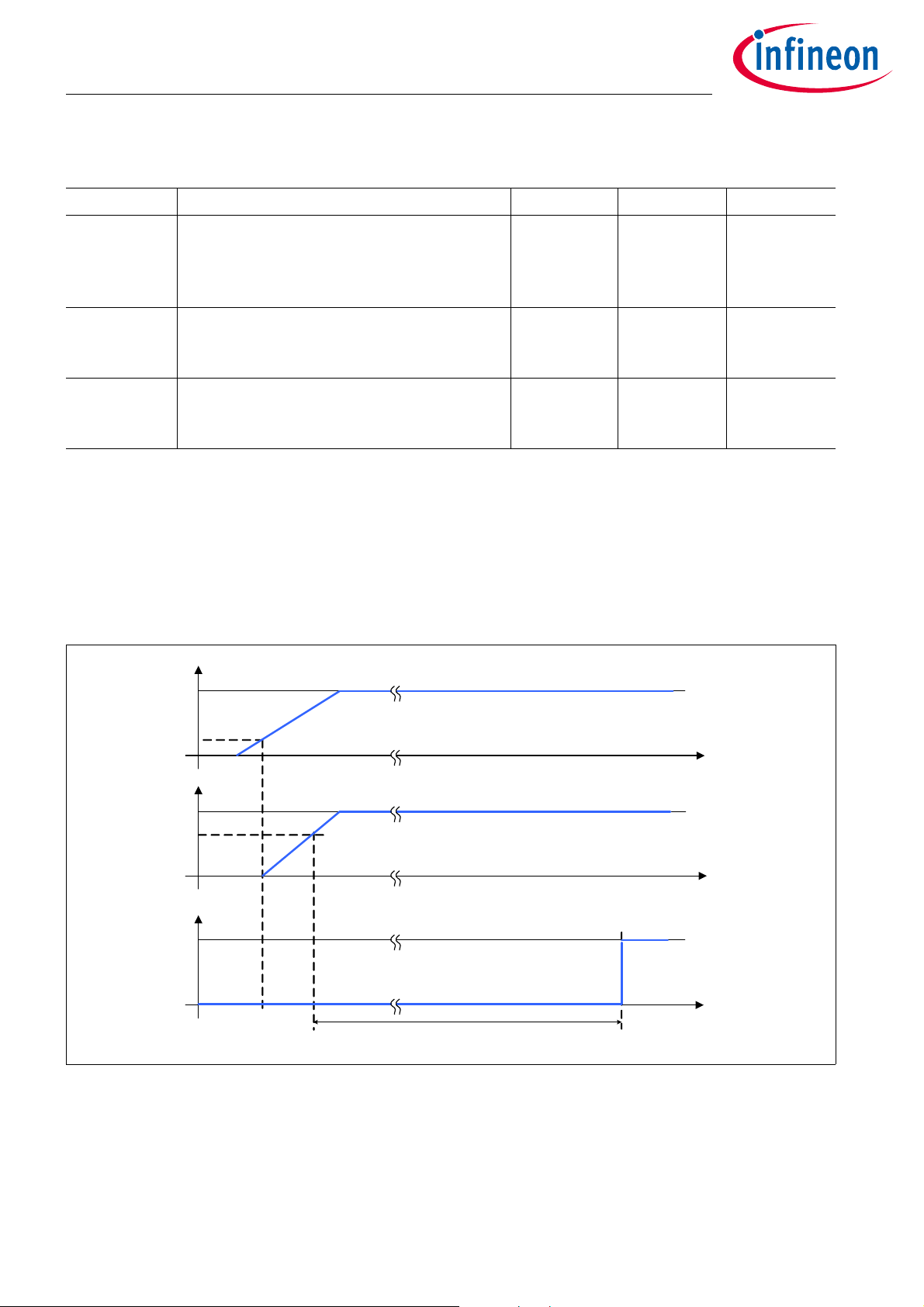
5.1.1 SBC Init Mode and Device Configuration
The SBC Init Mode is the mode where the hardware configuration of the SBC is stored and where the
microcontroller finishes the initialization phase. During the SBC Init Mode, the SBC can be configured in
normal operation or in SBC development mode (see also Chapter 5.1.7).
The hardware configuration is done monitoring the level of FO3/TEST pin. The pin FO3/Test is set as an input
and one internal pull-up resistor is activated (R
). The Table 5 shows possible hardware configurations.
TEST
Datasheet 19 Rev. 1.5
2019-09-27
Page 20
t
VCC1
t
RO
t
VS
V
POR,r
t
RD1
V
RT1,r
Configuration selection monitoring period
TLE9272QXV33
System Features
Table 5 SBC Configuration
Configuration Description FO3/Test Pin TEST CFG2_ STATE
Config 0 SBC Development Mode: no reset is triggered
01X
in case of a watchdog trigger failure. After the
Power-up, one arbitrary SPI command must
be sent.
Config 1 After missing the WD trigger for the first time,
the state of V
remains unchanged, FOx pins
CC1
Open or
>V
TEST,H
01
are active, SBC Restart Mode
Config 3 After missing the WD trigger for the second
time, the state of V
remains unchanged,
CC1
Open or
>V
TEST,H
00
FOx pins are active, SBC Restart Mode
An external pull-up resistor on CFG pin (R
) is needed for proper SBC configuration. The Config 1 or 3 is
CFG
selectable via SPI using CFG2 bit on HW_CTRL register.
The timing diagram for hardware configuration is shown in Figure 4.
The SBC starts up in SBC Init Mode after crossing the V
threshold (see also Chapter 13.3) or after a
POR,r
software reset command. As soon as the VCC1 voltage reaches the rising reset threshold V
configuration selection monitoring period starts for t
released and the window watchdog starts with a long open window t
(Reset Delay Time). After this time, the reset pin is
RD1
.
LW
RT1,r
, the
Figure 4 Hardware Configuration Selection Timing Diagram
During the long open window, the microcontroller shall finish its startup and initialization sequence. From this
transition mode, the SBC can be set, via SPI command, to SBC Normal Mode.
Any SPI command will bring the SBC to SBC Normal Mode even if it is an illegal SPI command (Chapter 14.2).
Datasheet 20 Rev. 1.5
2019-09-27
Page 21

TLE9272QXV33
System Features
No watchdog trigger during the long open window, will cause a watchdog failure and the device will enter in
SBC Restart Mode as shown in Table 5 and one reset event is generated.
In case of 3 consecutive reset events due to WD failures, it is possible not to generate additional reset by
setting the MAX_3_RST on WD_CTRL and the SBC will remain in SBC Normal or Stop Mode (SBC Restart Mode
not entered anymore). If the MAX_3_RST is set to 0, one reset event is generated for each missing watchdog
trigger.
Wake-up events are ignored during SBC Init Mode and will therefore be lost.
Note: Any SPI command will bring the SBC to SBC Normal Mode even if it is an illegal SPI command (see
Chapter 14.2)
Note: For a safe start-up, it is recommended to use the first SPI commands to trigger and to configure the
watchdog
Note: At power up no VCC1_UV will be issued nor will the FOx be triggered as long as VCC1 is below V
threshold and below the VS threshold for VS under voltage time out V
as long as VCC1 is below the selected V
released after t
(Reset Delay Time).
RD1
threshold. When VCC1 is above the V
RT1,r
. The RO pin will be kept low
S,UV_TO
threshold, the RO is
RT1,r
RT1,r
5.1.2 SBC Normal Mode
The SBC Normal Mode is the standard operating Mode for the SBC. All configurations have to be done in SBC
Normal Mode before entering a low-power mode. A wake-up event on CAN LIN1, LIN2, LIN3 and WK will create
an interrupt on pin INT however, no changes of SBC Mode will occur. The configuration options are listed
below:
• VCC1 is active (Buck regulator in PWM Mode)
• Boost Regulator can be configured and enabled or disabled. The module will start to work as soon as the
VS value is dropping below the selected threshold. For additional information, refer to Chapter 6.3.
• VCC2 can be switched ON or OFF (default off)
• CAN is configurable (OFF coming from SBC Init Mode; OFF or wake capable coming from SBC Restart Mode,
see also Chapter 5.1.5)
• LIN is configurable (OFF coming from SBC Init Mode; OFF or wake capable coming from SBC Restart Mode,
see also Chapter 5.1.5)
• Wake pin shows the input level and can be selected to be wake capable
• Cyclic wake can be configured with Timer1
• Watchdog is configurable
• FO1 and FO3 are OFF and FSI is active by default. FSI can be configured to be Fail-Safe Output (see also
Chapter 12.2). Coming from SBC Restart Mode, the FOx can be active or inactive (see also Chapter 12.1)
In SBC Normal Mode, there is the possibility of testing the FO outputs, i.e. to verify if setting the FOx pins to low
will create the intended behavior within the system. The FO outputs can be enabled and then disabled again
by the microcontroller by setting the FO_ON SPI bit. The feature is only intended for testing purposes.
5.1.3 SBC Stop Mode
The SBC Stop Mode is the first level technique to reduce the overall current consumption. In this mode VCC1
regulator is still active and supplying the microcontroller, which can enter into a power down mode. The VCC2
Datasheet 21 Rev. 1.5
2019-09-27
Page 22

TLE9272QXV33
System Features
could be enabled or disabled, CAN & LIN can be configured as Receive Only Mode, or wake capable or disable.
All kind of settings have to be done before entering SBC Stop Mode. In SBC Stop Mode any kind of SPI WRITE
commands are ignored and the SPI_FAIL bit is set, except for changing to SBC Normal Mode, triggering a SBC
Soft Reset, refreshing the watchdog, write the SYS_STAT_CTRL register as well as reading and clearing the SPI
status registers. A wake-up event on CAN, LIN1, LIN2, LIN3 and WK will create an interrupt on pin INT however, no change of SBC Mode will occur. The configuration options are listed below:
• VCC1 is ON (Buck regulator in PFM Mode)
• Boost regulator is fixed as configured in SBC Normal Mode. The module will start to work as soon as the VS
value drops below the selected threshold.
• VCC2 is fixed as configured in SBC Normal Mode
• CAN is fixed as configured in SBC Normal Mode
• LIN is fixed as configured in SBC Normal Mode
• WK is fixed as configured in SBC Normal Mode
• Cyclic wake is fixed as configured in SBC Normal Mode
Note: It is not possible to switch directly from SBC Stop Mode to SBC Sleep Mode. Doing so will also set the
SPI_FAIL flag and will bring the SBC into Restart Mode.
5.1.4 SBC Sleep Mode
The SBC Sleep Mode is the second level technique to reduce the overall current consumption to a minimum
needed to react on wake-up events. In this mode, VCC1 regulator is OFF and not supplying the microcontroller
anymore.The VCC2 supply can be configured to stay enabled. A wake-up event on CAN, LIN1, LIN2, LIN3 or WK
pin return the device to SBC Normal Mode via SBC Restart Mode and signal the wake source.
The configuration options are listed below:
•VCC1 is OFF
• Boost regulator is OFF
• VCC2 is fixed as configured in SBC Normal Mode
• Can must be set to CAN wake capable / CAN off before entering SBC Sleep Mode
• LIN is fixed as configured in SBC Normal Mode
• WK is fixed as configured in SBC Normal Mode
It is not possible to switch off all wake sources in SBC Sleep Mode. When a CAN or LIN transceiver is in its
Normal or Receive Only Mode, it counts as a wake source. In that case it changes automatically to Wake
Capable when the SBC enters SBC Sleep Mode.
All settings must be made before entering SBC Sleep Mode. If SPI configurations were sent to the SBC in SBC
Sleep Mode, the commands are ignored and there is no response from the SBC.
In order to enter SBC Sleep Mode successfully, all wake source signaling flags from WK_STAT_1 and
WK_STAT_2 need to be cleared. Otherwise, the device will immediately wake-up from SBC Sleep Mode by
going via SBC Restart to Normal Mode.
Note: As soon as the Sleep Command is sent, the Reset will go low to avoid any undefined behavior between SBC
and microcontroller
Datasheet 22 Rev. 1.5
2019-09-27
Page 23
TLE9272QXV33
System Features
5.1.5 SBC Restart Mode
There are multiple reasons to enter the SBC Restart Mode. The purpose of the SBC Restart Mode is to reset the
microcontroller:
• From SBC Normal and Stop Mode:
– Undervoltage on VCC1;
– Overvoltage on VCC1 (if VCC1_OV_ RST is set);
– Incorrect Watchdog triggering.
• From SBC Sleep and Fail-Safe Mode:
– Wake-up event on CAN or LINx or WK;
– After TDS2 (only from SBC Fail-Safe Mode. See also Chapter 13.8).
Table 6 contains detailed descriptions of the reason to restart.
Table 6 Reasons for Restart - State of SPI Status Bits after Return to Normal Mode
SBC Mode Event DEV_STAT WD_FAIL VCC1_UV VCC1_OV VCC1_SC
Normal Watchdog failure 01 01 or 10 0 x x
Normal VCC1 undervoltage reset 01 xx 1 0 x
Normal VCC1 overvoltage reset 01 xx 0 1 x
Sleep Mode Wake-up event 10 00 0 x x
Stop Mode Watchdog failure 01 01 or 10 0 x x
Stop Mode VCC1 undervoltage reset 01 xx 1 0 x
Stop Mode VCC1 overvoltage reset 01 xx 0 1 x
Fail-Safe Wake-up event 01 see “Reasons for Fail-Safe,
It is possible to change the entering into SBC Restart Mode due to watchdog trigger failure using MAX_3_RST
on WD_CTRL register. If the MAX_3_RST is set, after three consecutive resets, no further reset events are
generated in case of missing watchdog trigger (see also Chapter 13.2).
From SBC Restart Mode, the SBC automatically enters to SBC Normal Mode, i.e. the mode is left automatically
by the SBC without any microcontroller influence once the reset condition is no longer present and when the
reset delay time (t
Entering or leaving SBC Restart Mode will not disable the Fail outputs.
The following functions are activated / deactivated in SBC Restart mode:
• VCC1 is ON or ramping up
• Boost Regulator is fixed as configured in SBC Normal Mode. The module will start to work as soon as the
VS value drops below the selected threshold.
• VCC2 will be disabled if it was activated
• CAN is “woken” due to a wake-up event or OFF depending on previous SBC and transceiver mode (see also
Chapter 8). It is wake capable when it was in CAN Normal, Receive Only or wake capable mode before SBC
Restart Mode
) has expired. The Reset Output (RO) is released at the transition.
RD1
Table 7”
Datasheet 23 Rev. 1.5
2019-09-27
Page 24

TLE9272QXV33
System Features
• LINx are “woken” due to a wake-up event or OFF depending on previous SBC and transceiver mode (see
also Chapter 9). It is wake capable when it was in LINx Normal, Receive Only or wake capable mode before
SBC Restart Mode
• RO is pulled low during SBC Restart Mode
• SPI communication is ignored by the SBC, i.e. it is not interpreted
• SBC Restart Mode is signalled in the SPI register DEV_STAT by DEV_STAT bits.
Note: The VCC1 overvoltage reset is by default disabled. To enable it, the VCC1_OV_ RST has to be set. For
additional information, refer to Chapter 13.5.2.
5.1.6 SBC Fail-Safe Mode
The purpose of this mode is to bring the system in a safe status after a failure condition by turning off the VCC1
regulator and the RO will be LOW. After a wake-up event, the system can restart.
The Fail-Safe Mode is automatically reached in case of following events:
• overtemperature (TSD2) (see also Chapter 13.8);
• VCC1 is shorted to GND (see also Chapter 13.5.3).
In this case, the default wake sources are activated and the voltage regulators are switched OFF.
The mode will be maintained for at least typical 1s (t
other failure events to avoid any fast toggling behavior. All wake sources will be disabled during this time but
wake-up events will be stored. Stored wake-up events and wake-up events after this minimum waiting time
will lead to SBC Restart Mode. Leaving the SBC Fail-Safe Mode will not result in deactivation of the FOx pins.
The following functions are influenced during SBC Fail-Safe Mode:
• FO outputs are activated (see also Chapter 12)
•VCC1 is OFF
• Boost Regulator is OFF
•VCC2 is OFF
• CAN is wake capable
•LINx are wake capable
•WK is wake capable
• Cyclic wake is disabled, static sense is active with default filter time
• SPI communication is disabled because VCC1 is OFF
Table 7 Reasons for Fail-Safe - State of SPI Status Bits after Return to Normal Mode
) for a TSD2 event and typical 100ms (t
TSD2
FS,min
) for the
Mode Config Event DEV_STAT TSD2 WD_FAIL VCC1_UV VCC1_SC
Normal 1, 3 TSD2 01 1 xx x 0
Normal 1, 3, 4 VCC1 short to GND 01 x xx 1 1
Stop Mode 1, 3 TSD2 01 1 xx x 0
Stop Mode 1, 3 VCC1 short to GND 01 x xx 1 1
Datasheet 24 Rev. 1.5
2019-09-27
Page 25

TLE9272QXV33
System Features
5.1.7 SBC Development Mode
The SBC Development Mode is used during development phase of the application, especially for software
development. The mode is reached by setting the FO3/TEST pin to LOW when the device is in SBC Init Mode
and by sending an arbitrary SPI command. The SBC Init Mode is reached after the power-up.
When sending a software reset, it is no longer possible to enter SBC Development Mode.
The software reset is the SPI command that set the MODE bits in M_S_CTRL register.
SBC Development Mode can only be left by a power-down while FO3/TEST pin is high or open, or by setting
the MODE bits on M_S_CTRL SBC Software Reset regardless of the state of FO3/TEST.
In this mode, the watchdog does not need to be triggered. No reset is triggered because of watchdog failure.
When the FO3/TEST pin is left open, or connected to Vs during the start-up, the SBC starts into normal
operation. The FO3 pin has an integrated pull-up resistor, R
prevent the SBC device from starting in SBC Development Mode during normal life of the vehicle.
, (switched ON only during SBC Init Mode) to
TEST
Datasheet 25 Rev. 1.5
2019-09-27
Page 26
Cyclic Wake Configuration
Cyclic Wake starts automatically
INT is pulled low at the end of every
period
Select Timer Period in TIMER1_ CTRL
Periods: 10, 20 , 50 , 100 , 200ms, 1s, 2s
Select Timer1 as a wake source in
WK_CTRL_1
No interrupt will be generated,
if the t imer is not enabled as a wake source
TLE9272QXV33
System Features
5.2 Wake Features
The following wake sources are implemented in the device:
• Static Sense: WK input is permanently active (see Chapter 10)
• Cyclic Wake: internal wake source controlled via internal timer (see Chapter 5.2.1)
• CAN wake: Wake-up via CAN pattern (see Chapter 8)
• LIN wake: Wake-up via LIN bus (see Chapter 9)
The wake source must be set before entering in SBC Sleep Mode. In case of critical situation when the device
will be set into SBC Fail-Safe mode, all default wake sources will be activated.
5.2.1 Cyclic Wake
The cyclic wake feature is intended to reduce the quiescent current of the device and application.
For the cyclic wake feature, Timer 1 is configured as internal wake-up source and will periodically trigger an
interrupt in SBC Normal and Stop Mode based on the setting of TIMER1_CTRL.
The correct sequence to configure the cyclic wake is shown in Figure 5.
The sequence is as follows:
• Configure the respective period of Timer1 in the register TIMER1_CTRL.
• Enable Timer1 as a wake-up source in the register WK_CTRL_1.
Figure 5 Cyclic Wake: Configuration and Sequence
The cyclic wake function will start as soon as the Timer1 is enabled as wake-up source. An interrupt is
generated at the end of every period.
Datasheet 26 Rev. 1.5
2019-09-27
Page 27

TLE9272QXV33
System Features
5.2.2 Internal Timer
The integrated timer is typically used to wake up the microcontroller periodically (cyclic wake).
The following periods can be selected via the register TIMER1_CTRL:
• Period: 10ms / 20ms / 50ms / 100ms / 200ms / 1s / 2s
5.3 Supervision Features
The device offers various supervision features to support functional safety requirements. Refer to Chapter 13
for more information.
Datasheet 27 Rev. 1.5
2019-09-27
Page 28
GND
Buck
Converter
VCC1
BCKSW
VS
Feedforward
Soft Sta rt
Ramp
Generator
Bandgap
Reference
C1 C3
L1
L2
C4
Boost
Converter
SNSN
Comparator
Logic
SPI
C2
C5
T1
D2
D1
Vbat
BSTG
BSTD
SNSP
VSENSE
Rsense
V
SUP
TLE9272QXV33
DC/DC Regulator
6 DC/DC Regulator
6.1 Block Description
The SMPS module in the TLE9272QXV33 is implemented as a cascade of a step-up pre-regulator followed by a
step-down post-regulator. The step-up pre-regulator (DC/DC Boost converter) provides a VS level which
permits the step-down post-regulator (DC/DC Buck converter) to regulate without entering a low-drop
condition.
The SMPS module is active in SBC Normal, Stop and Restart Mode. In SBC Sleep and Fail-Safe Mode, the SMPS
module is disabled.
Figure 6 DC/DC Block Diagram
Functional Features:
•
3.3V SMPS (DC/DC) Buck converter with integrated high-side and low-side power switching transistor;
• SMPS (DC/DC) Boost converter as pre-regulator for low VSUP supply voltage (down to 3V) with
configurable output voltage via SPI;
• Fixed switching frequency for Buck and Boost converter in SBC Normal Mode in PWM (Pulse Width
Modulation);
• PFM (Pulse Frequency Modulation) for Buck converter in SBC Stop Mode to reduce the quiescent current;
Datasheet 28 Rev. 1.5
2019-09-27
Page 29
GND
Buck
Converter
VCC1
BCKSW
Feedforward
Soft St art
Ramp
Generator
Bandgap
Reference
L2
C4
Logic
C5
SPI
C1 C2
L1
D1
Vbat
VS
V
SUP
C3
TLE9272QXV33
DC/DC Regulator
• Automatic transition PFM to PWM in SBC Stop Mode;
• Soft start-up;
• Edge Shaping for better EMC performances for Buck and Boost regulator;
• Undervoltage monitoring on V
•Overvoltage detection on V
with adjustable reset level (refer to Chapter 13.5.1);
CC1
(refer to Chapter 13.5.2);
CC1
• Buck short circuit detection;
• Boost current peak detection with external shunt resistor.
6.2 Functional Description Buck converter
Figure 7 Buck Block Diagram
The DC/DC Buck converter is intended as post-regulator (VCC1) and it provides a step down converter function
transferring energy from VS to a lower output voltage with high efficiency (typically more than 80%). The
output voltage is
3.3V in a current range up to 750mA. It is regulated via a digital loop with a precision of ±2%.
It requires an external inductor and capacitor filter on the output switching pin (BCKSW). The Buck regulator
has two integrated power switches. The compensation of the regulation loop is done internally and no
additonal external components are needed.
A typical application example and external components proposal is available in Chapter 15.
The Buck converter is active in SBC Normal, Stop and Restart Mode and it is disabled in SBC Sleep and Fail safe
Mode.
Depending on the SBC Mode, the Buck converter works in two different modes:
• PWM Mode (Pulse Width Modulation): This mode is available in SBC Normal Mode, SBC Restart Mode and
SBC Stop Mode (only for automatic or manual PFM to PWM transitions. Please ref to Chapter 6.4.2). In
PWM, the Buck converter operates with a fix switching frequency (f
internally based on input voltage, output voltage and output current. The precision is ±2% or ±3% based
Datasheet 29 Rev. 1.5
). The duty cycle is calculated
BCK
2019-09-27
Page 30
Coil Current
Tristate TristateHS LS
Feedback Voltage VCC 1
PFM active
LVL
UCL
LCL
start biasing
&
oscillator
Quies cent Current
Iq Iq
OFF ON ONOFF
TLE9272QXV33
DC/DC Regulator
on input supply and output current range (refer to Figure 9 for more information). In PWM Mode, the Buck
converter is capable of a 100% duty cycle in case of low VS conditions. In order to reduce EMC, edge
shaping feature has been implemented to control the activation and deactivation of the two power
switches.
• PFM Mode (Pulse Frequency Modulation): This mode is activated automatically when the SBC Stop Mode
is entered. The PFM Mode is an asynchronous mode. PFM Mode does not have a controller switching
frequency. The switching frequency depends on conditions of the Buck regulator such as the following:
input supply voltage, output voltage, output current and external components. A typical timing diagram is
shown in Figure 8. The Buck converter in PFM Mode has a tolerance of ±4%. The transition from PFM mode
to PWM mode is described in Chapter 6.4.2.
Figure 8 Typical PFM timing diagram
6.2.1 Startup Procedure (Soft Start)
The Startup Procedure (Soft Start) permits to achieve the Buck regulator output voltage avoiding large
overshoot on the output voltage. This feature is activated during the power-up, from SBC Sleep to Restart
Mode and from SBC Fail-Safe to SBC Restart Mode.
When the Buck regulator is activated, it starts with a minimum duty cycle and the regulation loop maintains it
for a limited number of switching periods. After this first phase, the duty cycle is increased by a fixed value and
kept for a limited number of switching periods. This procedure is repeated until the target output voltage
value of the Buck regulator is reached. As soon as the Buck regulator output voltage is reached, the regulation
loop starts to operate normally using PWM Mode adjusting the duty cycle according the Buck input and output
voltages and the Buck regulator output current.
6.2.2 Buck regulator Status register
The register SMPS_STAT contains information about the open or short conditions on BCKSW pin and if the
Buck regulator is outside the 12% nominal output voltage range. No SBC Mode or configuration is triggered if
one bit is set in the SMPS_STAT register.
Datasheet 30 Rev. 1.5
2019-09-27
Page 31

TLE9272QXV33
DC/DC Regulator
6.2.3 External components
The Buck converter needs one inductor and output capacitor filter. The inductor has a fixed value of 47µH.
Secondary parameter such as saturation current must be selected based on the maximum current capability
needed in the application.
The output capacitors filter are 47µF (typically, an electrolytic capacitor) in parallel with 10µF (ceramic
capacitor). This configuration is intended for Buck regulator functionary and keep the total ESR lower than 1Ω
in all temperature range. For additional information, refer to Chapter 15.1.
Datasheet 31 Rev. 1.5
2019-09-27
Page 32

VS
C1 C3
L1
Boost
Converter
Rsense
SNSN
Comparat or
Logic
SPI
C2
T1
D2
D1
Vbat
BSTG
BSTD
SNSP
VS
VSENSE
V
SUP
TLE9272QXV33
DC/DC Regulator
6.3 Functional Description Boost
Figure 9 Boost Block Diagram
The Boost converter is intended as pre-regulator and it provides a step up converter function. It transfers
energy from an input supply VSUP (battery voltage after the reverse protection circuit) to a higher output
voltage (VS) with high efficiency (typically more than 80%).
The regulator integrates the gate driver for external power switching and external passive components are
necessary in particular: input buffer capacitor on the battery voltage, inductor, power switching transistor,
sense resistor for overcurrent detection, freewheeling diode and filter capacitor. A typical application
example is available in Chapter 15.
In SBC Normal Mode and in SBC Stop Mode, the Boost regulator can be enabled via SPI (register HW_CTRL, bit
BOOST_EN). The boost output voltage has to be selected using BOOST_V bit. The BOOST_V on HW_CTRL
permits to select the minimum V
or the output voltage V
BST1_1
BST2_1
.
The activation thresholds vary according to the output voltage selected. Table 8 shows the possible activation
thresholds and the hysteresis including the respective SPI setting.
Table 8 Boost activation thresholds
Boost Output Voltage Activation threshold Hysteresis SPI Setting
V
BST1_1
V
BST2_1
If the Boost regulator is enabled, it switches ON automatically when VSENSE falls below the threshold voltage
V
BST,TH1
is set and it can be clear only if VSENSE is above the V
or V
BST,TH2
Figure 10 shows the typical timing for enabling the Boost converter.
V
BST,TH1
V
BST,TH2
and switches OFF when crossing the threshold plus respective hysteresis. The bit BST_ACT
V
V
BST,HYS1
BST,HYS2
BST,TH1
BOOST_V = 1
BOOST_V = 0
or V
BST,TH2
.
Datasheet 32 Rev. 1.5
2019-09-27
Page 33

BST_ACT
001
BSTG
VS
VSUP
V
BST,THx
V
BST,HYSx
peakOC
SNSTH
SENSE
I
V
R
,
,
=
TLE9272QXV33
DC/DC Regulator
Figure 10 Boost converter activation
The Boost regulator works in PWM Mode with a fixed frequency (f
) and a tolerance of ±5%.
BST
If the Boost is enabled in SBC Stop Mode, the SBC quiescent current is increased.
6.3.1 Boost Regulator Status register
The register SMPS_STAT contains information about the open or short conditions on Boost pin’s including
loss of GND detection. No SBC mode or configuration is triggered if one bit is set on SMPS_STAT register.
6.3.2 External Components
The Boost converter requires a number of external components such as the following: input buffer capacitor
on the battery voltage, inductor, power switching transistor, sense resistor for overcurrent detection,
freewheeling diode and filter capacitors.
For recommend devices and values, refer to Chapter 15.1.
The inductor can be selected in one range from 22µH up to 47µH. The value and the secondary parameters
(e.g. saturation current) have to be selected in according to the maximum current capability required by the
application.
The characterization is performed with the suggested external power MOSFET Infineon BSS606N. Other
MOSFETs can be used. However, the functionality has to be checked in the application considering the gate
driver current capability (P_6.5.27 and P_6.5.9) and maximum output current requirements.
6.3.2.1 Peak Overcurrent Detection
The Boost converter implement one peak overcurrent detection using one external shunt resistor. For typical
application, refer to Chapter 15.1.
As soon as the Boost converter detects one peak overcurrent, the regulation loop reduces the duty cycle in
order to reduce the peak current on the external MOSFET.
The shunt resistor can be calculated based on V
Datasheet 33 Rev. 1.5
and using Equation (6.1).
TH,SNS
(6.1)
2019-09-27
Page 34

Normal Mode Stop Mode
t
SPI Commands
Buck modulation PWM
PWM
Auto PFM ↔ PWM
t
lag
TLE9272QXV33
DC/DC Regulator
Example: for an overcurrent peak detection of 2.1A, the resistor is typically 0.1Ω.
6.4 Power Scenarios
The chapter describes the features and performance of the Buck and Boost regulators according to SBC mode.
6.4.1 Buck and Boost in SBC Normal Mode
In SBC Normal Mode, the Buck regulator operates in PWM mode with fixed switching frequency. The
microcontroller and other loads on the ECU are typically supplied with a
functions for Buck regulator are available in SBC Normal Mode (for more details, refer to Chapter 13.5.1,
Chapter 13.5.2, Chapter 13.5.3 and Chapter 13.8).
3.3V output voltage. All supervision
6.4.2 Buck and Boost in SBC Stop Mode Operation
The SBC Stop Mode operation is intended to reduce the total amount of quiescent current while still providing
supply for microcontroller. In order to achieve this, the Buck regulator automatically changes the modulation
from PWM (Pulse Width Modulation) to PFM (Pulse Frequency Modulation) when entering SBC Stop Mode. In
case the Boost regulator in SBC Stop Mode is enabled and running, it operates only in PWM mode.
6.4.2.1 Automatic Transition from PFM to PWM in SBC Stop Mode
In SBC Stop Mode, the Buck converter operates in PFM mode by default to reduce current consumption. If
more current is needed, an automatic transition from PFM to PWM modulation is implemented. When the
Buck regulator output current exceeds the I
PWM and an INT event is generated. In addition, the PFM_PWM bit on WK_STAT_1 is set.
In order to set the Buck modulation again in PFM, it is necessary to write a Stop Mode command to M_S_CTRL
register. This command has to be sent when the required Buck output current is below the I
threshold.
When entering SBC Stop Mode, the automatic transition from PFM to PWM mode is activated after the time t
which is the transition time where the Buck regulator loop changes the modulation technique. Two possible
values can be configured via SPI command.
The Figure 11 shows the timing transition from SBC Normal to SBC Stop Mode.
PFM-PWM,TH
threshold, the Buck module changes the modulation to
PFM-PWM,TH
lag
,
Figure 11 Transition from SBC Normal to SBC Stop Mode
The t
The automatic transition can be disabled by setting the bit PWM_AUTO to 0 in the HW_CTRL register.
Datasheet 34 Rev. 1.5
is always present in case of PWM to PFM transition.
lag
2019-09-27
Page 35

TLE9272QXV33
DC/DC Regulator
6.4.2.2 Manual Transition from PFM to PWM in SBC Stop Mode
The PFM to PWM transition can also be controlled by the microcontroller or an external signal, directly by
using the WK pin as a trigger signal if a additional current is required in SBC Stop Mode.
When the PWM_BY_ WK bit is set to 1, the DC/DC regulator can be switched from PFM to PWM using the WK pin.
A LOW level at the WK pin will switch the Buck converter to PFM mode, a HIGH level will switch it to PWM Mode.
In this configuration, the filter time is not taken into account because a defined signal from µC or external
source is expected.
If the PWM_BY_ WK bit is set to 0, the PFM modulation is used.
Datasheet 35 Rev. 1.5
2019-09-27
Page 36

TLE9272QXV33
DC/DC Regulator
6.4.2.3 SBC Stop to Normal Mode Transition
The microcontroller sends an SPI command to switch from SBC Stop Mode to SBC Normal Mode. In this
transition, the Buck regulator changes the modulation from PFM to PWM.
Once the SPI command for the SBC Normal Mode transition is received the current is able to rise above the
specified maximum Stop Mode current (I
If the transition from SBC Stop Mode to SBC Normal Mode is carried out when the Boost is enabled and
operating, it will continue to operate without any changes.
PFM-PWM,TH
).
6.4.3 Buck and Boost in SBC Sleep and Fail Safe Mode
In SBC Sleep or Fail Safe Mode, the Buck and Boost converter are off and not operating. The lowest quiescent
current is achievable.
6.4.3.1 SBC Sleep/Fail Safe Mode to Normal Mode Transition
In case of a wake-up event from WK pin or transceivers, the SBC will be set SBC Restart Mode and as soon as
the reset is released, into SBC Normal Mode.
In SBC Restart Mode, the Buck regulator is activated and ramping. The Boost regulator is activated and
ramping again (in case the VS is below the selected threshold) in according the configuration selected in SBC
Normal Mode. As soon as the Buck output voltage exceeds the reset threshold, the RO pin is released.
Datasheet 36 Rev. 1.5
2019-09-27
Page 37

TLE9272QXV33
DC/DC Regulator
6.5 Electrical Characteristics
Table 9 Electrical Characteristics
T
= -40 °C to +150 °C; VS = 5.5 V to 28 V; all voltages with respect to ground, positive current flowing into pin
j
(unless otherwise specified)
Parameter Symbol Values Unit Note or
Min. Typ. Max.
Test Condition
Buck Regulator
Output Voltage SBC Normal
Mode
V
CC1,out1
3.23 3.3 3.36 V Normal Mode (PWM)
1mA < I
6.3V < V
Output Voltage SBC Normal
Mode
V
CC1,out2
3.23 3.3 3.36 V
1)
Normal Mode (PWM)
= 400mA
I
VCC1
V
= 4V
S
Boost Disable
Output Voltage SBC Stop Mode V
CC1,out3
3.16 3.3 3.43 V Stop Mode (PFM)
1mA < I
PWM,TH
6.3V < VS < 18V
Output Voltage SBC Stop Mode V
CC1,out4
3.18 3.3 3.39 V Stop Mode (PFM)
1mA < I
6.3V < V
Power Stage on-resistance
High-Side
Power Stage on-resistance
R
DSON1,HS
R
DSON1,LS
––1.3Ω VS = 6.5V
=100mA
I
VS
––1.3Ω I
=100mA P_6.5.20
BCKSW
Low-Side
VCC1
< 28V
S
VCC1
VCC1
< 18V
S
< 750mA
< I
PFM-
< 50mA
Number
P_6.5.12
P_6.5.24
P_6.5.13
P_6.5.41
P_6.5.3
Buck switching frequency f
Threshold automatic
transition PFM to PWM
Transition time from PWM to
PFM
Transition time from PWM to
PFM
BCK
I
PFM-
PWM,TH
t
lag
t
lag
405 450 495 kHz Normal Mode (PWM) P_6.5.5
80 110 150 mA
–1–ms1) PWM_TLAG=1
1)
Stop Mode
6.3V < V
S
P_6.5.14
< 18V
P_6.5.15
(on HW_CTRL)
– 100 – µs
1)
PWM_TLAG=0
P_6.5.16
(on HW_CTRL)
Boost Regulator
Boost Voltage 1 V
BST1_1
6.32 6.65 6.88 V
2)
SBC Normal Mode
V
= 3V
SUP
I
= 550mA
VS
P_6.5.11
Boost enabled
BOOST_V = 1
Datasheet 37 Rev. 1.5
2019-09-27
Page 38

TLE9272QXV33
DC/DC Regulator
Table 9 Electrical Characteristics (cont’d)
= -40 °C to +150 °C; VS = 5.5 V to 28 V; all voltages with respect to ground, positive current flowing into pin
T
j
(unless otherwise specified)
Parameter Symbol Values Unit Note or
Test Condition
2)
SBC Normal Mode
V
= 3V
SUP
I
= 450mA
VS
Boost Voltage 2 V
BST2_1
Min. Typ. Max.
7.6 8 8.4 V
Boost enabled
BOOST_V = 0
Boost Switch ON/OFF voltage
1 threshold
V
BST,TH1
6.35 7 7.5 V Boost enabled
V
falling
S
BOOST_V = 1
Boost Switch ON/OFF
hysteresis 1
Boost Switch ON/OFF voltage
2 threshold
V
BST,HYS1
V
BST,TH2
300 500 600 mV Boost enabled
BOOST_V = 1
9.5 10 10.5 V Boost enabled
V
falling
S
BOOST_V = 0
Boost Switch ON/OFF
hysteresis 2
BSTG Source Current - Charge
current
V
BST,HYS2
I
BSTG,sour
0.9 1 1.2 V Boost enabled
BOOST_V = 0
-50 -35 -25 mA V
> 3V
SUP
Boost enabled
Number
P_6.5.6
P_6.5.7
P_6.5.8
P_6.5.32
P_6.5.33
P_6.5.27
BSTG Sink Current - Discharge
current
BSTG rise switching time t
I
BSTG,sink
BSTG,rise
25 35 50 mA V
–30–ns1) V
> 3V
SUP
Boost enabled
> 3V
SUP
P_6.5.9
P_6.5.28
20% - 80%
C
= 470pF
BSTG
BSTG fall switching time t
BSTG,fall
–30–ns1) V
SUP
> 3V
P_6.5.29
20% - 80%
C
= 470pF
BSTG
Over current shunt voltage
V
TH,SNS
threshold
Boost switching frequency f
1) Not subject to production test; specified by design.
2) Values verified in characterization with Boost converter specified in Chapter 15.1. Not subject to production test;
specified by design. Refer to Figure 13 for additional information.
BST
199 210 221 mV Boost enable
> 3V
V
SUP
405 450 495 kHz Normal Mode (PWM) P_6.5.10
P_6.5.21
Datasheet 38 Rev. 1.5
2019-09-27
Page 39

400
450
500
550
600
650
700
750
800
4 4.1 4.2 4.3 4.4 4.5 4.6 4.7 4.8 4.9 5 5.1 5.2 5.3 5.4 5.5 6.5 8 10 12 18 20 24 28
I
VCC1
(mA)
VS(V)
VCC1 tolerance +/-2%
3 4 5 6 7 8
0.2
0.4
0.6
0.8
1
1.2
1.4
V
SUP
(V)
I
VS
(A)
Boost Output 6.65V
Boost Output 8V
TLE9272QXV33
DC/DC Regulator
Figure 12 Maximum DCDC Buck current capability versus VS.
Note: The Figure 12 is based on characterization results over temperature with external components specified
in Chapter 15.1.
Figure 13 Maximum DCDC Boost current capability versus VSUP(TLE9271..3QX version).
Note: Figure 13 is based on simulation results (specified by design), with Boost converter external components
specified in Chapter 15.1.
Datasheet 39 Rev. 1.5
2019-09-27
Page 40

GND
Overtemperature
Shutdown
1
Bandgap
Refe re nc e
VS2
State
Machine
VCC2
INH
Vref
TLE9272QXV33
Voltage Regulator 2
7 Voltage Regulator 2
7.1 Block Description
Figure 14 Module Block Diagram
Functional Features
• 5Vlow-drop voltage regulator
• Protected against short to supply voltage, e.g. for off-board sensor supply
• Can also be used for CAN supply
• VCC2 undervoltage monitoring. Please refer to Chapter 13.6 for more information
• Can be active in SBC Normal, SBC Stop, and SBC Sleep Mode (not SBC Fail-Safe Mode)
• VCC2 switch off after entering SBC Restart Mode. Switch off is latched, LDO must be enabled via SPI after
shutdown.
• Overtemperature protection
• ≥ 470nF ceramic capacitor at output voltage for stability, with ESR < 1Ω @ f = 10 kHz, to achieve the voltage
regulator control loop stability based on the safe phase margin (Bode diagram).
• Output current capability up to I
Datasheet 40 Rev. 1.5
VCC2,lim
.
2019-09-27
Page 41

TLE9272QXV33
Voltage Regulator 2
7.2 Functional Description
In SBC Normal Mode, VCC2 can be switched on or off via SPI.
For SBC Stop- or Sleep Mode, the VCC2 has to be switched on or off before entering the respective SBC mode.
The output current of VCC2 is limited at I
The VS2 pin is the dedicated supply pin for VCC2. VS2 can be connected to VS and therefore to the boost
output, or directly from battery after the reverse protection input diode.
For low-quiescent current, the output voltage tolerance is decreased in SBC Stop Mode because only a lowpower mode regulator (with lower accuracy V
increases (typ. more than 1.5mA), then the high-power mode regulator will also be enabled to support an
optimum dynamic load behavior. When both power mode regulators are active, the VCC2 quiescent current
will the typical increase by 2.9mA.
If the load current on VCC2 decreases (typically below 1.3mA), then the low-quiescent current mode is
resumed again disabling the high-power mode regulator.
Both regulators are active in SBC Normal Mode.
Note: If the VCC2 output voltage is supplying external off-board loads, the application must consider the series
resonance circuit built by cable inductance and decoupling capacitor at load. Sufficient damping must
be provided.
VCC2,lim
CC2,out5
.
) will be active for small loads. If the load current on VCC2
Datasheet 41 Rev. 1.5
2019-09-27
Page 42

TLE9272QXV33
Voltage Regulator 2
7.3 Electrical Characteristics
Table 10 Electrical Characteristics
T
= -40 °C to +150 °C; VS2 = 5.5 V to 28 V; all voltages with respect to ground, positive current flowing into pin
j
(unless otherwise specified)
Parameter Symbol Values Unit Note or
Test Condition
1)
SBC Normal Mode
10µA < I
Output Voltage including line
and Load regulation
V
CC2,out1
Min. Typ. Max.
4.9 5.0 5.1 V
6.5V < VS2 < 28V
Output Voltage including line
and Load regulation
V
CC2,out2
4.9 5.0 5.1 V
1)
SBC Normal Mode
10µA < IVCC2 < 80mA
6V < VS2 < 28V
Output Voltage including line
and Load regulation
Output Voltage including line
and Load regulation
V
CC2,out3
V
CC2,out4
4.85 5.0 5.15 V
4.97 – 5.07 V
1)
10µA < IVCC2 < 60mA
SBC Normal Mode
2)
SBC Normal Mode
8V < VS2 < 18V
10µA < I
25°C< T
Output Voltage including line
and Load regulation
Output Voltage including line
and Load regulation
Output Drop V
Over Current limitation I
V
CC2,out5
V
CC2,out6
CC2,d1
VCC2,lim
4.9 5.05 5.2 V SBC Stop, Sleep Mode
1mA < I
4.9 5.05 5.25 V SBC Stop, Sleep Mode
10µA < I
– – 500 mV I
VCC2
V
S2
= 30mA
= 5V
100 – 7502)mA current flowing out of
pin
V
= 0V
CC2
VS2 = 13.5V
1) In SBC Stop Mode, the specified output voltage tolerance applies from I
consumption.
2) Not subject to production test, specified by design.
> 3mA but with increased current
CC2
< 100mA
VCC2
< 5mA
VCC2
<125°C
j
< 3mA
VCC2
< 1mA
VCC2
Number
P_7.3.1
P_7.3.2
P_7.3.19
P_7.3.18
P_7.3.3
P_7.3.20
P_7.3.4
P_7.3.5
Datasheet 42 Rev. 1.5
2019-09-27
Page 43

TLE9272QXV33
Voltage Regulator 2
Figure 15 VCC2 pass device on-resistance during low drop operation for I
= 30mA
CC2
Datasheet 43 Rev. 1.5
2019-09-27
Page 44

TXDCAN
Output
Stage
Driver
Temp.-
Protection
CANH
CANL
+
timeout
RXD CA N
Receiver
MUX
V
CC1
SPI Mode
Control
To SPI diagnostic
can block .v sd
VCA N
V
CC1
R
TD
Wake
Receiver
Vs
VCAN
TLE9272QXV33
High Speed CAN Transceiver
8 High Speed CAN Transceiver
8.1 Block Description
Figure 16 Functional Block Diagram
8.2 Functional Description
The Controller Area Network (CAN) transceiver part of the SBC provides HIGH-Speed (HS) differential mode
data transmission (up to 5Mbaud) and reception in automotive and industrial applications. It works as an
interface between the CAN protocol controller and the physical bus lines compatible with ISO 11898-2: 2016
as well as SAE J2284.
The CAN transceiver offers low power modes to reduce current consumption. This supports networks with
partially powered down nodes. To support software diagnostic functions, a CAN Receive-only Mode is
implemented.
It is designed to provide excellent passive behavior when the transceiver is switched off (mixed networks,
clamp 15/30 applications).
A wake-up from the CAN Wake capable Mode is possible via a message on the bus. Thus, the microcontroller
can be powered down or idled and will be woken up by the CAN bus activities.
Datasheet 44 Rev. 1.5
2019-09-27
Page 45

SBC Normal Mode
SBC Mode CAN Transceiver Mode
SBC Stop Mode
SBC Sleep Mode
SBC Restart Mode
Receive Only Normal Mode OFFWake Capable
Receive Only OFFWake Capable
OFFWoken
1)
OFF
2)
Wake Capable
2)
Behavior after SBC Restart M ode - no t coming from SBC Sleep Mode due to a wake up of the res pective transceiver:
If the transceivers were configured to Normal Mode, or Receive Only Mode, th en the mod e wil l be changed to Wake Capable.
If it was Wake Capabl e, th en it will remai n Wak e Cap able. If it was off before SBC Rest art Mode, then i t wil l remain off.
1)
After a wake event on CAN Bus.
2)
Must be set to CAN wak e capable / CAN OFF mode before entering SBC Sleep Mode.
SBC Fail-Safe Mode Wake Capable
Example:
- 11 bit identifier + 8Byte data
- Arbitration Phase 500kbps
- Data Phase 2Mbps
à average bit rate 1.14Mbps
CAN Header
Data phase
(Byte 0 – Byte 7)
CAN Footer
Standard CAN
message
CAN Header
Data phase
(Byte 0 – Byte 7)
CAN Footer
CAN FD with
reduced bit time
TLE9272QXV33
High Speed CAN Transceiver
The CAN transceiver is designed to withstand the severe conditions of automotive applications and to support
12V applications.
The transceiver can also be configured as wake-capable in order to save power and to ensure a safe transition
from SBC Normal to Sleep Mode (to avoid losing messages).
Figure 17 shows the possible transceiver mode transition when changing the SBC mode.
Figure 17 CAN Mode Control Diagram
CAN FD Support
CAN FD stands for ‘CAN with Flexible Data Rate’. It is based on the well established CAN protocol as specified
in ISO 11898-1. CAN FD still uses the CAN bus arbitration method. The benefit is that the bit rate can be
increased by switching to a shorter bit time at the end of the arbitration process and then returning to the
longer bit time at the CRC delimiter before the receivers transmit their acknowledge bits. See also Figure 18.
In addition, the effective data rate is increased by allowing longer data fields. CAN FD allows the transmission
of up to 64 data bytes compared to the 8 data bytes from the standard CAN.
Figure 18 Bite rate Increase with CAN FD vs. Standard CAN
Datasheet 45 Rev. 1.5
2019-09-27
Page 46

t
V
CAN DIFF
t
CAN,E N
t
V
TXDCAN
t
CAN
Mode
CAN
NORM AL
CAN
OFF
CAN,E N
t
recessive TXDCAN
level required before
start of transmission
t
CAN, EN
n ot en sur ed, n o
transmission on bus
CAN,E N
t
Co rrect seq uenc e,
Bus is enabled after
t
CAN, EN
t
CAN, EN
n ot en sur ed,
no tra nsmi ssion on bus
recessive
TXDCAN
level required
Dom inant
Recessive
TLE9272QXV33
High Speed CAN Transceiver
CAN FD has to be supported by both physical layer and the CAN controller. If the CAN controller cannot
support CAN FD, then the respective CAN node must at least tolerate CAN FD communication. This CAN FD
tolerant mode is implemented in the physical layer.
8.2.1 CAN OFF Mode
The CAN OFF Mode is the default mode after the SBC has powered up. It is available in all SBC Modes and is
used to completely stop CAN activities or when CAN communication is not needed. In CAN OFF Mode, a wakeup event on the bus will be ignored.
8.2.2 CAN Normal Mode
The CAN Transceiver is enabled via SPI. CAN Normal Mode is designed for normal data transmission/reception
within the HS CAN network. This mode is available in SBC Normal Mode.
Transmission
The signal from the microcontroller is applied to the TXDCAN input of the SBC. The bus driver switches the
CANH/L output stages to transfer this input signal to the CAN bus lines.
Enabling sequence
The CAN transceiver requires an enabling time t
before a message can be sent on the bus. This means
CAN,EN
that the TXDCAN signal can only be pulled LOW after the enabling time. If this is not ensured, then the TXDCAN
needs to be set back to HIGH (=recessive) until the enabling time is over. Only the next dominant bit will be
transmitted on the bus. Figure 19 shows different scenarios and explanations for CAN enabling.
Figure 19 CAN Transceiver Enabling Sequence
Reduced Electromagnetic Emission
To reduce electromagnetic emissions (EME), the bus driver controls CANH/L slopes symmetrically.
Reception
Analog CAN bus signals are converted into digital signals at RXDCAN via the differential input receiver.
Datasheet 46 Rev. 1.5
2019-09-27
Page 47

Ini
Bias off
1
Bias off
2
Bias off
3
Bias on
Wait
Bias off
Bus recessive > t
WAKE1
Bus dominant > t
WAKE1
t
WAKE2
expired
Bus recessive > t
WAKE1
Bus dominant > t
WAKE1
t
WAKE2
expired
Entering CAN Normal
or CAN Recive Only
Entering CAN wake
capable
TLE9272QXV33
High Speed CAN Transceiver
8.2.3 CAN Receive Only Mode
In CAN Receive Only Mode (RX only), the driver stage is disabled but reception is still operational. This mode is
accessible by an SPI command in SBC Normal Mode and in SBC Stop Mode.
Note: The transceiver is still working properly in Receive Only mode even if VCAN is not available because of an
independent receiver supply.
8.2.4 CAN Wake Capable Mode (Wake-up Pattern)
This mode can be used in SBC Stop, Sleep, Restart and Normal Mode by programming via SPI and it is used to
monitor bus activities. It is automatically accessed in SBC Fail-Safe Mode. A wake-up pattern on the bus results
in a change of behavior of the SBC, as described in Table 11. As a signal to the microcontroller, the RXDCAN
pin is set to low and will stay low until the CAN transceiver changes to a different mode. After a wake-up
pattern event, the transceiver can be switched to CAN Normal Mode via SPI for bus communication.
As shown in Figure 20, a wake-up pattern is signaled on the bus by two consecutive dominant bus levels for
at least t
t
Wake1
Wake1
and shorter than t
(filter time t > t
Wake2
) and less than t
Wake1
.
, each separated by a recessive bus level greater than
Wake2
Figure 20 CAN Wake-up Pattern Detection (WUP) according to the Definition in ISO 11898-5
Rearming the Transceiver for Wake Capability
After a BUS wake-up pattern event, the transceiver is woken. However, the CAN transceiver mode bits will still
show wake capable (=‘01’) so the RXDCAN signal will be pulled LOW. There are two possibilities for enabling
the CAN transceiver’s wake capable mode again after a wake-up event:
Datasheet 47 Rev. 1.5
2019-09-27
Page 48

TLE9272QXV33
High Speed CAN Transceiver
• The CAN transceiver mode must be toggled, i.e. switched from Wake Capable Mode to CAN Normal Mode,
CAN Receive Only Mode or CAN Off, before switching to CAN Wake Capable Mode again.
• Rearming occurs automatically when the SBC changes to SBC Stop, or SBC Fail-Safe Mode to ensure wakeup capability.
• If the SBC is in SBC Stop Mode, the CAN is rearmed automatically if the SBC is set again in SBC Stop Mode.
• CAN must be set to CAN Wake Capable or CAN OFF mode before entering SBC Sleep Mode.
Notes
1. It is necessary to clear the CAN Wake-Up bit CAN_WU to become wake capable again. It is sufficient to toggle
the CAN Mode.
2. The CAN module is supplied by an internal voltage when in CAN Wake Capable Mode, i.e. the module must not
be supplied through the VCAN pin during this time. Before changing the CAN Mode to Normal Mode, the supply
of VCAN has to be activated first.
Wake-Up in SBC Stop and Normal Mode
In SBC Stop Mode, if a wake-up pattern is detected, it is always signaled by the INT output and in the
WK_STAT_1 SPI register. It is also signaled by RXDCAN pulled to LOW. The same applies for the SBC Normal
Mode. The microcontroller should set the device from SBC Stop Mode to SBC Normal Mode; there is no
automatic transition to Normal Mode.
For functional safety reasons, the watchdog will be automatically enabled in SBC Stop Mode after a bus wakeup event in case it was disabled before (if bit WD_EN_WK_BUS was configured to HIGH before).
Wake-Up in SBC Sleep Mode
Wake-up is possible via a CAN message. The wake-up pattern automatically transfers the SBC into the SBC
Restart Mode and from there to Normal Mode the corresponding RXDCAN pin is set to LOW. The
microcontroller is able to detect the LOW signal on RXDCAN and to read the wake source out of the
WK_STAT_1 register via SPI. No interrupt is generated when coming out of Sleep Mode. The microcontroller
can now, for example, switch the CAN transceiver into CAN Normal Mode via SPI to start communication.
Table 11 Action due to CAN Bus Wake-Up
SBC Mode SBC Mode after Wake VCC1 INT RXDCAN
Normal Mode Normal Mode ON LOW LOW
Stop Mode Stop Mode ON LOW LOW
Sleep Mode Restart Mode Ramping Up HIGH LOW
Restart Mode Restart Mode ON HIGH LOW
Fail-Safe Mode Restart Mode Ramping Up HIGH LOW
8.2.5 TXDCAN Time-out Feature
If the TXDCAN signal is dominant for a time t > t
disables the transmission of the signal at the bus, setting the TXDCAN pin to recessive. This is implemented to
prevent the bus from being blocked permanently due to an error. The transmitter is disabled and fixed to
recessive. The CAN SPI control bits (CAN on BUS_CTRL_1) remain unchanged and the failure is stored in the
Datasheet 48 Rev. 1.5
TXDCAN_TO
, in CAN Normal Mode, the TXDCAN time-out function
2019-09-27
Page 49

TLE9272QXV33
High Speed CAN Transceiver
SPI flag CAN_FAIL. The CAN transmitter stage is activated again after the dominant time-out condition is
removed and the transceiver is automatically switched back to CAN Normal Mode.
8.2.6 Bus Dominant Clamping
If the HS CAN bus signal is dominant for a time t > t
dominant clamping is detected and the SPI bit CAN_FAIL is set. The transceiver configuration stays
unchanged.
BUS_CAN_TO
, in CAN Normal and Receiver Only Mode, a bus
8.2.7 VCAN Undervoltage Detection
The voltage at the VCAN supply pin is monitored in CAN Normal and Receive Only Mode. If the HS CAN
transceiver is set in CAN Wake Capable Mode, the VCAN supply pin is enable after that a valid WUP is detected.
In case of VCAN undervoltage a signalization via SPI bit VCAN_UV is triggered and the TLE9272QXV33 disables
the transmitter stage. If the CAN supply reaches a higher level than the under voltage detection threshold
(VCAN > V
configuration stays unchanged.
), the transceiver is automatically switched back to CAN Normal Mode. The transceiver
CAN_UV
Datasheet 49 Rev. 1.5
2019-09-27
Page 50

TLE9272QXV33
High Speed CAN Transceiver
8.3 Electrical Characteristics
Table 12 Electrical Characteristics
T
= -40 °C to +150 °C; VS = 5.5 V to 28 V; V
j
respect to ground, positive current flowing into pin (unless otherwise specified)
= 4.75 V to 5.25 V; RL = 60Ω; CAN Normal Mode; all voltages with
CAN
Parameter Symbol Values Unit Note or
Min. Typ. Max.
Test Condition
CAN Supply Voltage
CAN Supply undervoltage
detection threshold
V
CAN_UV
4.45 – 4.85 V CAN Normal Mode,
hysteresis included
CAN Bus Receiver
Differential Receiver
Threshold Voltage,
recessive to dominant edge
V
diff,rd_N
– 0.800.90V V
= V
diff
-12V ≤ VCM(CAN) ≤
12V;
CAN Normal Mode
Dominant state differential
input voltage range
V
diff_D_range
0.9 – 8.0 V
1)
V
= V
diff
-12V ≤ VCM(CAN) ≤
12V;
CAN Normal Mode
Differential Receiver
Threshold Voltage,
dominant to recessive edge
V
diff,dr_N
0.50 0.60 – V V
= V
diff
-12V ≤ V
12V;
CAN Normal Mode
Recessive state differential
input voltage range
V
diff_R_range
-3.0 – 0.5 V
1)
V
= V
diff
-12V ≤ VCM(CAN) ≤
12V;
CAN Normal Mode
Common Mode Range CMR -12 – 12 V
1)
- V
CANH
CANH -VCANL
CANH
(CAN) ≤
CM
CANH
CANL;
- V
- V
CANL;
;
CANL;
Number
P_8.3.1
P_8.3.2
P_8.3.50
P_8.3.3
P_8.3.51
P_8.3.4
CANH, CANL Input
Resistance
R
i
20 40 50 kΩ CAN Normal / Wake
Capable Mode;
P_8.3.5
Recessive state
Differential Input Resistance R
diff
-2V ≤ V
40 80 100 kΩ CAN Normal / Wake
CANH/L
≤ +7V
P_8.3.6
Capable Mode;
Recessive state
Input Resistance Deviation
between CANH and CANL
Input Capacitance CANH,
DR
C
-2V ≤ V
i
in
-3 – 3 %
–2040pF2)V
1)
Recessive state
V
CANH=VCANL
TXDCAN
≤ +7V
CANH/L
P_8.3.7
=5V
= 5V P_8.3.8
CANL versus GND
Differential Input
C
diff
–1020pF2)V
= 5V P_8.3.42
TXDCAN
Capacitance
Datasheet 50 Rev. 1.5
2019-09-27
Page 51

TLE9272QXV33
High Speed CAN Transceiver
Table 12 Electrical Characteristics (cont’d)
= -40 °C to +150 °C; VS = 5.5 V to 28 V; V
T
j
respect to ground, positive current flowing into pin (unless otherwise specified)
= 4.75 V to 5.25 V; RL = 60Ω; CAN Normal Mode; all voltages with
CAN
Parameter Symbol Values Unit Note or
Test Condition
12V;
CAN Wake Capable
Wake-up Receiver
Threshold Voltage,
recessive to dominant edge
V
diff, rd_W
Min. Typ. Max.
– 0.8 1.15 V -12V ≤ VCM(CAN) ≤
Mode
Wake-up Receiver
Dominant state differential
input voltage range
V
diff_D_range_
W
1.15 – 8.0 V
1)
V
= V
diff
-12V ≤ VCM(CAN) ≤
12V;
CAN Wake Capable
Mode
Wake-up Receiver
Threshold Voltage,
dominant to recessive edge
V
diff, dr_W
0.4 0.7 – V -12V ≤ VCM(CAN) ≤
12V;
CAN Wake Capable
Mode
Wake-up Receiver
Recessive state differential
input voltage range
V
diff_R_range_
W
-3.0 – 0.4 V
1)
V
= V
diff
-12V ≤ VCM(CAN) ≤
12V;
CAN Wake Capable
Mode
CANH
CANH
- V
- V
CANL;
CANL;
Number
P_8.3.9
P_8.3.52
P_8.3.10
P_8.3.53
CAN Bus Transmitter
CANH/CANL Recessive
Output Voltage
(CAN Normal Mode)
CANH/CANL Recessive
Output Voltage
(CAN Wake Capable Mode)
CANH, CANL Recessive
Output Voltage Difference
= V
V
diff
CANH
- V
CANL
(CAN Normal Mode)
CANH, CANL Recessive
Output Voltage Difference
= V
V
diff
CANH
- V
CANL
(CAN Wake Capable Mode)
CANL Dominant Output
Voltage
V
CANL/H_NM
V
CANL/H_LP
V
diff_r_N
V
diff_r_W
V
CANL
2.0 – 3.0 V CAN Normal Mode
V
TXDCAN
= V
cc1
;
no load
-0.1 – 0.1 V CAN Wake Capable
Mode;
V
TXDCAN
= V
cc1
;
no load
-500 – 50 mV CAN Normal Mode;
V
TXDCAN
= V
cc1
;
no load
-200 – 200 mV CAN Wake Capable
Mode;
V
TXDCAN
= V
cc1
;
no load
0.5 – 2.25 V
3)
CAN Normal Mode;
TXDCAN
= 5V;
CAN
= 0V;
≤ 65Ω
L
V
V
50Ω ≤ R
P_8.3.11
P_8.3.43
P_8.3.12
P_8.3.44
P_8.3.13
Datasheet 51 Rev. 1.5
2019-09-27
Page 52

TLE9272QXV33
High Speed CAN Transceiver
Table 12 Electrical Characteristics (cont’d)
= -40 °C to +150 °C; VS = 5.5 V to 28 V; V
T
j
respect to ground, positive current flowing into pin (unless otherwise specified)
= 4.75 V to 5.25 V; RL = 60Ω; CAN Normal Mode; all voltages with
CAN
Parameter Symbol Values Unit Note or
Test Condition
3)
CAN Normal Mode;
V
TXDCAN
V
= 5V;
CAN
CANH Dominant Output
Voltage
V
CANH
Min. Typ. Max.
2.75 – 4.5 V
50Ω ≤ R
CANH, CANL Dominant
Output Voltage Difference
= V
V
diff
CANH
- V
CANL
V
diff_d_N
1.5 2.0 2.5 V
3)
CAN Normal Mode;
V
TXDCAN
V
= 5V;
CAN
50Ω ≤ R
CANH, CANL Output Voltage
Difference Slope, recessive
to dominant
V
diff_slope_rd
––70V/us1)30% to 70% of
measured
differential bus
voltage,
C
= 100 pF, RL = 60 Ω
L
CANH, CANL Output Voltage
Difference Slope, dominant
to recessive
CANH, CANL Dominant
Output Voltage Difference
= V
V
diff
CANH
- V
CANL
on
extended bus load range
CANH Short Circuit Current I
CANL Short Circuit Current I
V
diff_slope_dr
V
diff_d_N_ext
CANHsc
CANLsc
––70V/us1)70% to 30% of
measured
differential bus
1.5 – 5.0 V
voltage,
C
= 100 pF, RL = 60 Ω
L
1)
CAN Normal Mode;
V
TXDCAN
V
= 5V;
CAN
R
= 2240Ω
L
-100 -80 -50 mA CAN Normal Mode;
V
CANHshort
50 80 100 mA CAN Normal Mode;
V
CANLshort
= 0V;
≤ 65Ω
L
= 0V;
≤ 65Ω
L
= 0V;
= -3 V
= 18 V
Number
P_8.3.14
P_8.3.15
P_8.3.54
P_8.3.55
P_8.3.58
P_8.3.16
P_8.3.17
Leakage Current I
CANH,lk
I
CANL,lk
–57.5µAVS = V
0V ≤ V
4)
R
= 0V;
CAN
CANH,L
= 0 / 47kΩ
test
P_8.3.18
≤ 5V;
Receiver Output RXDCAN
HIGH level Output Voltage V
LOW Level Output Voltage V
RXDCAN,H
RXDCAN,L
0.8 ×
V
CC1
––VCAN Normal Mode;
––0.2 ×
V
cc1
= -2 mA
I
RXDCAN
VCAN Normal Mode;
= 2 mA
I
RXDCAN
P_8.3.19
P_8.3.20
Transmission Input TXDCAN
HIGH Level Input Voltage
V
TXDCAN,H
Threshold
Datasheet 52 Rev. 1.5
––0.7 ×
V
cc1
VCAN Normal Mode;
P_8.3.21
recessive state
2019-09-27
Page 53

TLE9272QXV33
High Speed CAN Transceiver
Table 12 Electrical Characteristics (cont’d)
= -40 °C to +150 °C; VS = 5.5 V to 28 V; V
T
j
respect to ground, positive current flowing into pin (unless otherwise specified)
= 4.75 V to 5.25 V; RL = 60Ω; CAN Normal Mode; all voltages with
CAN
Parameter Symbol Values Unit Note or
Test Condition
dominant state
1)
valid transmitted
LOW Level Input Voltage
Threshold
TXDCAN Input Hysteresis V
TXDCAN Pull-up Resistance R
CAN Transceiver Enabling
Time
V
TXDCAN,L
TXDCAN,hys
TXDCAN
t
CAN,EN
Min. Typ. Max.
0.3 ×
V
cc1
– 0.12 ×
––VCAN Normal Mode;
–mV
V
cc1
20 40 80 kΩ - P_8.3.24
81318µs7) CSN = HIGH to first
TXDCAN dominant
Dynamic CAN-Transceiver Characteristics
Driver Symmetry
= V
V
SYM
CANH
+ V
CANL
V
SYM
4.5 – 5.5 V
5)
CAN Normal Mode;
V
TXDCAN
V
= 5V;
CAN
= 4.7nF;
C
SPLIT
50Ω ≤ R
Min. Dominant Time for Bus
Wake-up
t
Wake1
0.5 – 3.5 µs -12V ≤ VCM(CAN) ≤
12V;
Vdiff ≤ 3V
CAN Wake capable
Mode
Wake-up Time-out,
Recessive Bus
BUS Bias reaction time t
t
Wake2
bias
0.5 – 10 ms
– – 250 µs
7)
CAN Wake capable
Mode
7)
CAN Wake capable
Mode
V
= 5V;
CAN
= 100pF;
C
L
C
= 100pF;
GND
R
= 60Ω
L
Loop delay
(recessive to dominant)
Loop delay
(dominant to recessive)
t
LOOP,f
t
LOOP,r
– 150 255 ns
– 150 255 ns
5)
CAN Normal Mode;
C
= 100pF;
L
= 60 Ω;
R
L
V
= 5V;
CAN
C
RXDCAN
5)
CAN Normal Mode;
C
= 100pF;
L
= 60Ω;
R
L
V
= 5V;
CAN
C
RXDCAN
= 0V / 5V;
≤ 60Ω
L
= 15 pF
= 15 pF
Number
P_8.3.22
P_8.3.23
P_8.3.25
P_8.3.45
P_8.3.26
P_8.3.27
P_8.3.57
P_8.3.28
P_8.3.29
Datasheet 53 Rev. 1.5
2019-09-27
Page 54

TLE9272QXV33
High Speed CAN Transceiver
Table 12 Electrical Characteristics (cont’d)
= -40 °C to +150 °C; VS = 5.5 V to 28 V; V
T
j
respect to ground, positive current flowing into pin (unless otherwise specified)
= 4.75 V to 5.25 V; RL = 60Ω; CAN Normal Mode; all voltages with
CAN
Parameter Symbol Values Unit Note or
Test Condition
C
= 100pF;
L
R
= 60 Ω;
L
= 5V
V
CAN
= 100pF;
C
L
R
= 60Ω;
L
V
= 5V
CAN
C
= 100pF;
L
= 60Ω;
R
L
V
= 5V;
CAN
C
RXDCAN
= 100pF;
C
L
R
= 60 Ω;
L
V
= 5V;
CAN
C
RXDCAN
= 100pF;
C
L
R
= 60Ω;
L
V
= 5V;
CAN
= 15pF;
C
RXD
t
= 500ns;
bit(TXD)
Propagation Delay
TXDCAN LOW to bus
dominant
Propagation Delay
TXDCAN HIGH to bus
recessive
Propagation Delay
bus dominant to RXDCAN
LOW
Propagation Delay
bus recessive to RXDCAN
HIGH
Received Recessive bit width t
t
d(L),T
t
d(H),T
t
d(L),R
t
d(H),R
bit(RXD)
Min. Typ. Max.
– 50 – ns CAN Normal Mode;
– 50 – ns CAN Normal Mode;
– 100 – ns CAN Normal Mode;
– 100 – ns CAN Normal Mode;
400 – 550 ns CAN Normal Mode;
Parameter definition
in according to
Figure 22.
Number
P_8.3.30
P_8.3.31
P_8.3.32
= 15 pF
P_8.3.33
= 15 pF
P_8.3.39
Transmitted Recessive bit
width
t
bit(BUS)
435 – 530 ns CAN Normal Mode;
C
= 100pF;
L
R
= 60 Ω;
L
= 5 V;
V
CAN
C
= 15 pF;
RXD
t
= 500ns;
bit(TXD)
P_8.3.40
Parameter definition
in according to
Figure 22.
Datasheet 54 Rev. 1.5
2019-09-27
Page 55

TLE9272QXV33
High Speed CAN Transceiver
Table 12 Electrical Characteristics (cont’d)
= -40 °C to +150 °C; VS = 5.5 V to 28 V; V
T
j
respect to ground, positive current flowing into pin (unless otherwise specified)
= 4.75 V to 5.25 V; RL = 60Ω; CAN Normal Mode; all voltages with
CAN
Parameter Symbol Values Unit Note or
Test Condition
C
= 100pF;
L
R
= 60Ω;
L
= 5V;
V
CAN
C
= 15pF;
RXD
t
= 500ns;
bit(TXD)
Receiver timing symmetry6)Δt
Rec
Min. Typ. Max.
-65 – 40 ns CAN Normal Mode;
Parameter definition
in according to
Figure 22.
Received Recessive bit width t
bit(RXD)
120 – 220 ns CAN Normal Mode;
C
= 100pF;
L
= 60Ω ;
R
L
V
= 5V;
CAN
= 15pF;
C
RXD
t
= 200ns;
bit(TXD)
Parameter definition
in according to
Figure 22.
Number
P_8.3.41
P_8.3.46
Transmitted Recessive bit
width
Receiver timing symmetry
TXDCAN Permanent
Dominant Time-out
6)
t
bit(BUS)
Δt
Rec
t
TXDCAN_TO
155 – 210 ns CAN Normal Mode;
C
= 100pF;
L
R
= 60 Ω;
L
= 5 V;
V
CAN
C
= 15 pF;
RXD
t
= 200ns;
bit(TXD)
P_8.3.47
Parameter definition
in according to
Figure 22.
-45 – 15 ns CAN Normal Mode;
C
= 100pF;
L
= 60Ω;
R
L
V
= 5V;
CAN
C
= 15pF;
RXD
= 200ns;
t
bit(TXD)
P_8.3.48
Parameter definition
in according to
Figure 22.
–1.85–ms7)CAN Normal Mode P_8.3.34
BUS Permanent Dominant
t
BUS_CAN_TO
–1.85–ms7)CAN Normal Mode P_8.3.35
Time-out
Datasheet 55 Rev. 1.5
2019-09-27
Page 56

t
d(L),R
t
V
DIF F
t
loop,f
t
d(H), R
t
loop,r
t
d(L),T
t
GND
V
TXDCAN
V
IO
t
d(H),T
V
diff, rd _N
V
diff, dr _N
t
GND
0.2 x V
IO
0.8 x V
IO
V
RXD CAN
V
IO
TLE9272QXV33
High Speed CAN Transceiver
1) Not subject to production test, specified by design.
2) Not subject to production test, specified by design, S2P - Method; f = 10Mhz.
3) Voltage value valid for time < t
4) R
5) V
between (Vs /VCAN) and 0V (GND).
tests
shall be observed during dominant and recessive state and also during the transition dominant to recessive and
SYM
TXDCAN_TO
vice versa while TxD is simulated by a square signal (50% duty cycle), a frequency of 1MHz.
6) t
Rec=tbit(RXD)
-t
bit(BUS)
.
7) Not subject to production test, tolerance defined by internal oscillator tolerance.
.
Figure 21 Timing Diagrams for Dynamic Characteristics
Datasheet 56 Rev. 1.5
2019-09-27
Page 57

500mV
TXDCAN
70%
30%
RXDCAN
V
diff
=CANH-CANL
30%
70%
900mV
5x t
Bit(TXD)
t
Bit(TXD)
t
Loop_f
t
Bit(Bus)
t
Loo p_r
t
Bit(RX D)
TLE9272QXV33
High Speed CAN Transceiver
Figure 22 From ISO 11898-2: tloop, tbit(TXD), tbit(Bus), tbit(RXD) Definitions
Datasheet 57 Rev. 1.5
2019-09-27
Page 58

Driver
Temp.-
Pro t ection
Current
Limit
Output
Stage
TxD Input
Receiver
RX DLIN
LIN
TX DLIN
VLIN
R
BUS
Filter
Timeout
R
TXD L I N
VCC1
To SPI Diagnostic
SPI Mode Control
VCC1
Wake
Receiver
Vs
TLE9272QXV33
LIN Transceiver
9 LIN Transceiver
9.1 Block Description
Figure 23 Block Diagram
9.1.1 LIN Specifications
The LIN network is standardized by international regulations. The device is compliant with the LIN2.2
specification. The physical layer specification LIN2.2 is a superset of the previous LIN specifications, like LIN
2.0, LIN2.1 or LIN 1.3. The integrated LIN transceivers are according to the LIN2.2 standard.
The device is compliant to the physical layer standard SAE-J2602-2. The SAE-J2602-2 standard differs from the
LIN2.2 standard mainly by the lower data rate (10.4 kbps).
Datasheet 58 Rev. 1.5
2019-09-27
Page 59

SBC Normal Mode
SBC Mode LIN Transceiver Mode
SBC Stop Mode
SBC Sleep Mode
SBC Restart Mode
Receive Only Normal Mode OFFWake Capable
Receive Only OFFWake Capable
OFFWoken
1
OFFWake Capable
Behavior after SBC Restart Mode - not coming from SBC Sleep Mode due to a wake up of the respec tive transceiver :
If the transceiv ers had been configured to Normal Mode, or Receive Only Mode , then the mode will be changed to Wake
Capable . If it was Wake Capable , then it will remain Wake Capable . If it had been OFF before SBC Restart Mode , then it
will remain OFF .
1
after a wake event on LIN Bus
SBC Fail-Safe Mode Wake Capable
TLE9272QXV33
LIN Transceiver
9.2 Functional Description
The LIN Bus is a single wire, bidirectional bus, used for in-vehicle networks. The LIN transceivers implemented
inside the TLE9272QXV33 are the interface between the microcontroller and the physical LIN Bus. The digital
output data from the microcontroller are driven to the LIN bus via the TXDLIN input pin on the TLE9272QXV33.
The transmit data stream on the TXDLIN input is converted to a LIN bus signal with an optimized slew rate to
minimize the EME level of the LIN network. The RXDLIN output sends back the information from the LIN bus to
the microcontroller. The receiver has an integrated filter network to suppress noise on the LIN Bus and to
increase the EMI (Electromagnetic Immunity) level of the transceiver.
Two logical states are possible on the LIN Bus according to the LIN Specification 2.2.
Every LIN network consists of a master node and one or more slave nodes. To configure the TLE9272QXV33 for
master node applications, a resistor in the range of 1kΩ and a reverse diode must be connected between the
LIN bus and the power supply VS.
The different transceiver modes can be controlled using the SPI LIN1, LIN2, LIN3 bits.
The transceiver can also be configured to wake capable in order to save current and to ensure a safe transition
from SBC Normal to Sleep Mode (to avoid losing messages).
Figure 24 shows the possible transceiver mode transitions when changing the SBC Mode.
Figure 24 LIN Mode Control Diagram
9.2.1 LIN OFF Mode
The LIN OFF Mode is the default mode after power-up of the SBC. It is available in all SBC Modes and is
intended to completely stop LIN activities or when LIN communication is not needed. In LIN OFF Mode, a
wake-up event on the bus will be ignored.
Datasheet 59 Rev. 1.5
2019-09-27
Page 60

t
V
LIN_BUS
t
LIN,EN
t
V
TXDLIN
t
LIN
Mod e
LIN
NORMA L
LIN OFF
LIN,EN
t
LIN,EN
t
recessive TXDLIN leve l
required bevore start of
transmission
t
LIN, EN
not ensured, n o
transmissio n o n b us
Correct sequence,
Bus is enabled aftert
LIN, EN
t
LIN, EN
not ensured,
no transmission on bus
rece ssive TXDL IN
leve l req uired
Recessive
Dominant
LIN_enabling_sequence.vsd
TLE9272QXV33
LIN Transceiver
9.2.2 LIN Normal Mode
The LIN Transceiver is enabled via SPI in SBC Normal Mode. LIN Normal Mode is designed for normal data
transmission/reception within the LIN network. The Mode is available only in SBC Normal Mode.
Transmission
The signal from the microcontroller is applied to the TXDLIN input of the SBC. The bus driver switches the
LIN output stage to transfer this input signal to the LIN bus line.
Enabling sequence
The LIN transceiver requires an enabling time t
the TXDLIN signal can only be pulled LOW after the enabling time. If this is not ensured, then the TXDLIN needs
to be set back to HIGH (=recessive) until the enabling time is completed. Only the next dominant bit will be
transmitted on the bus. Figure 25 shows different scenarios and explanations for LIN enabling.
before a message can be sent on the bus. This means that
LIN,EN
Figure 25 LIN Transceiver Enabling Sequence
Reduced Electromagnetic Emission
To reduce electromagnetic emissions (EME), the bus driver controls LIN slopes symmetrically. The
configuration of the different slopes is described in Chapter 9.2.8.
Reception
Analog LIN bus signals are converted into digital signals at RXDLIN via the input receiver.
9.2.3 LIN Receive Only Mode
In LIN Receive Only Mode (RX only), the driver stage is disabled but reception is still possible. This mode is
accessible by an SPI command and is available in SBC Normal and SBC Stop Mode.
9.2.4 LIN Wake Capable Mode
This mode can be used in SBC Stop, Sleep, Restart and Normal Mode by programming via SPI and it is used to
monitor bus activities. It is automatically accessed in SBC Fail-Safe Mode. A wake up is detected, if a recessive
to dominant transition on the LIN bus is followed by a dominant level of longer than t
, followed by a
WK,Bus
Datasheet 60 Rev. 1.5
2019-09-27
Page 61

TLE9272QXV33
LIN Transceiver
dominant to recessive transition. The dominant to recessive transition will cause a wake up of the LIN
transceiver. A wake-up results different behavior of the SBC, as described in Table 13. As a signalization to the
microcontroller, the RXDLIN pin is set LOW and will stay LOW until the LIN transceiver is changed to any other
mode. After a wake-up event, the transceiver can be switched to LIN Normal Mode for communication.
Table 13 Action due to a LIN BUS Wake-up
SBC Mode SBC Mode after Wake VCC1 INT RXDLIN
Normal Mode Normal Mode ON LOW LOW
Stop Mode Stop Mode ON LOW LOW
Sleep Mode Restart Mode Ramping Up HIGH LOW
Restart Mode Restart Mode ON HIGH LOW
Fail-Safe Mode Restart Mode Ramping up HIGH LOW
Rearming the transceiver for wake capability
After a BUS wake-up event, the transceiver is woken. However, the LIN1, LIN2, LIN3 transceiver mode bits will
still show wake capable (=‘01’) so that the RXDLIN signal will be pulled low. The wake-capable mode of the LIN
transceiver can be reenabled in one of two ways after a wake-up event:
• By toggling the LIN transceiver mode, i.e. switched to LIN Normal Mode, LIN Receive Only Mode or LIN Off,
before switching to LIN Wake Capable Mode again.
• Occurs automatically when the SBC changes to SBC Stop, SBC Sleep, or SBC Fail-Safe Mode to ensure
wake-up capability.
• if the SBC is in SBC Stop Mode, the LIN’s are rearmed automatically if the SBC is set again in SBC Stop Mode.
Wake-Up in SBC Stop and SBC Normal Mode
In SBC Stop Mode, if a wake-up is detected, it is signaled by the INT output and in the WK_STAT_2 SPI register.
It is also signaled by RXDLIN put to LOW. The same applies for the SBC Normal Mode. The microcontroller
should set the device to SBC Normal Mode; there is no automatic transition to Normal Mode.
For functional safety reasons, the watchdog will be automatically enabled in SBC Stop Mode after a Bus wakeup event in case it was disabled before (if bit WD_EN_WK_BUS was configured to HIGH before).
Wake-Up in SBC Sleep Mode
Wake-up is possible via a LIN message (filter time t > t
SBC Restart Mode and from there to Normal Mode. The corresponding RXDLIN pin in set to LOW. The
microcontroller is able to detect the low signal on RXDLIN and to read the wake source out of the WK_STAT_2
register via SPI. No interrupt is generated when coming out of Sleep Mode. The microcontroller can now
switch the LIN transceiver into LIN Normal Mode via SPI to start communication.
). The wake-up automatically transfers the SBC to
WK,Bus
9.2.5 TXDLIN Time-Out Feature
If the TXDLIN signal is dominant for the time t >t
transmitter output stage temporarily. The transceiver remains in Recessive state. The TXDLIN time-out
function prevents the LIN bus from being blocked by a permanent LOW signal on the TXDLIN pin caused by a
Datasheet 61 Rev. 1.5
BUS_LIN_TO
, the TXDLIN time-out function deactivates the LIN
2019-09-27
Page 62

TXDLIN
LIN
t
torec
t
timeout
Normal Communication
Normal Communication
TXDLIN Time-Out due to
microcontroller error
Release after TXDLIN
Time-out
Recovery of the
microcontroller error
t
t
TLE9272QXV33
LIN Transceiver
failure. The failure is stored in the SPI flag LIN1_FAIL, LIN2_FAIL, LIN3_FAIL on BUS_STAT_1 and
BUS_STAT_2 registers. The LIN transmitter stage is activated again after the dominant time-out condition is
removed.
The TXDLIN Time-Out feature can be disabled with SPI bit LIN_TXD_ TO for all LINs at the same time.
Figure 26 TXDLIN Time-Out Function
9.2.6 Bus Dominant Clamping
If the LIN bus signal is dominant for a time t > t
BUS_LIN_TO
dominant clamping is detected and the SPI bits LIN1_FAIL, LIN2_FAIL, LIN3_FAIL and are set. The
transceiver configuration stays unchanged.
9.2.7 Undervoltage Detection
In case the supply voltage VLIN is dropping below the VLIN undervoltage detection threshold (VLIN < V
the TLE9272QXV33 will set the LINx in Receive Only Mode (the transmitter is disabled). The receiver stage is
active. If the power supply VLIN reaches a higher level than the VLIN undervoltage detection threshold (VLIN >
V
9.2.8 Slope Selection
), the TLE9272QXV33 continues with normal operation.
LIN,UVD
The LIN transceiver offers a LIN Low-Slope Mode for 10.4kBaud communication and a LIN Normal-Slope Mode
for 20kBaud communication. The only difference is the behavior of the transmitter. In LIN Low-Slope Mode,
the
transmitter uses a lower slew rate to further reduce the EME compared to Normal-Slope Mode. This complies
with SAE J2602 requirements.
in LIN Normal or Receieve Only Mode, then a bus
LIN,UVD
),
Datasheet 62 Rev. 1.5
2019-09-27
Page 63

TLE9272QXV33
LIN Transceiver
By default, the device works in LIN Normal-Slope Mode. The selection of LIN Low-Slope Mode is done by an SPI
bit LIN_LSM and will become effective as soon as CSN goes ‘HIGH’ for all LINx. Only the LIN Slope is changed.
The selection is accessible in SBC Normal Mode only.
9.2.9 Flash Programming via LIN
The device allows LIN flash programming, e.g. of another LIN Slave with a communication of up to 115 kbps.
This feature is enabled by de-activating the slope control mechanism via a SPI command (bit LIN_FLASH) and
will become effective as soon as CSN goes ‘HIGH’ for all LINx. The SPI bit can be set in SBC Normal Mode.
Note: It is recommended to perform flash programming only at nominal supply voltage VS = 13.5V to ensure
stable data communication.
Datasheet 63 Rev. 1.5
2019-09-27
Page 64

TLE9272QXV33
LIN Transceiver
9.3 Electrical Characteristics of the LIN Transceiver
Table 14 Electrical Characteristics: LIN Transceiver
T
= -40 °C to +150 °C, V
j
into pin (unless otherwise specified)
Parameter Symbol Values Unit Note or Test Condition Number
Receiver Output (RXDLIN pin)
= 5.5 V to 18 V, RL = 500 Ω, all voltages with respect to ground, positive current flowing
LIN
Min. Typ. Max.
HIGH Level Output Voltage V
LOW Level Output Voltage V
RXDLIN,H
RXDLIN,L
Transmission Input (TXDLIN pin)
HIGH Level Input Voltage V
TXDLIN Input Hysteresis V
LOW Level Input Voltage V
TXDLIN Pull-up Resistance R
TXDLIN,H
TXDLIN,hys
TXDLIN,L
TXDLIN
LIN Bus Receiver (LIN Pin)
Receiver Threshold Voltage,
V
Bus,rd
Recessive to Dominant Edge
Receiver Dominant State V
Receiver Threshold Voltage,
Bus,dom
V
Bus,dr
Dominant to Recessive Edge
Receiver Recessive State V
Receiver Center Voltage V
Receiver Hysteresis V
Wake-up Threshold Voltage V
Dominant Time for Bus
Bus,rec
Bus,c
Bus,hys
Bus,wk
t
WK,Bus
Wake-up
0.8 ×
V
CC
––0.2 ×
0.7 ×
V
CC
–0.2 ×
––0.3 ×
20 40 80 kΩ V
0.4 ×
V
LIN
––0.4 ×
– 0.55 ×
0.6 ×
V
LIN
0.475
× V
0.07 ×
V
LIN
0.40 ×
V
LIN
––VI
V I
V
CC
––VRecessive State P_9.3.3
–V
V
CC
VDominant State P_9.3.5
V
CC
0.45 ×
V
V
– – V LIN2.2 Param 18 P_9.3.10
0.5 ×
V
LIN
0.1 ×
V
0.5 ×
V
– V P_9.3.7
LIN
V LIN2.2 Param. 17 P_9.3.8
V
LIN
LIN
LIN
LIN
LIN
0.60 ×
V
LIN
0.525
× V
0.175
× V
0.6 ×
V
LIN
VP_9.3.9
V LIN2.2 Param 19 P_9.3.11
LIN
V V
LIN
V – P_9.3.13
30 – 150 µs
= -2 mA
RXDLIN
V
= V
bus
S
= 2 mA
RXDLIN
V
= 0 V
bus
1)
= 0 V P_9.3.6
TXDLIN
bus,hys
= V
bus,rec
- V
bus,dom
LIN2.2 Param 20
2)
P_9.3.1
P_9.3.2
P_9.3.4
P_9.3.12
P_9.3.14
Datasheet 64 Rev. 1.5
2019-09-27
Page 65

TLE9272QXV33
LIN Transceiver
Table 14 Electrical Characteristics: LIN Transceiver (cont’d)
= -40 °C to +150 °C, V
T
j
into pin (unless otherwise specified)
Parameter Symbol Values Unit Note or Test Condition Number
LIN Bus Transmitter (LIN Pin)
Bus Serial Diode Voltage
Drop
= 5.5 V to 18 V, RL = 500 Ω, all voltages with respect to ground, positive current flowing
LIN
Min. Typ. Max.
V
serdiode
0.4 0.7 1.0 V
1)
V
TXDLIN
= V
CC1
;
P_9.3.15
LIN2.2 Param 21
Bus Recessive Output
Voltage
Bus Short Circuit Current I
Leakage Current
Loss of Ground
Leakage Current
Loss of Battery
Leakage Current
Driver Off
Leakage Current
Driver Off
Bus Pull-up Resistance R
LIN Input Capacitance C
Receiver propagation delay
bus dominant to RXDLIN
LOW
V
BUS,ro
BUS,sc
I
BUS,lk1
I
BUS,lk2
I
BUS,lk3
I
BUS,lk4
BUS
BUS
t
d(L),R
0.8 ×
V
LIN
40 100 150 mA V
–VLINVV
= high Level P_9.3.16
TXDLIN
= 18V;
BUS
LIN2.2 Param 12
-1000 -450 20 µA V
= 0V;
LIN
-12V ≤ V
BUS
≤ 6V;
LIN2.2 Param 15
––20µAV
= 0 V;
LIN
0V ≤ V
BUS
≤ 18V;
LIN2.2 Param 16
-1 – – mA V
––20µAV
= 18 V;
LIN
V
= 0 V;
BUS
LIN2.2 Param 13
= 8 V;
LIN
V
= 18 V;
BUS
LIN2.2 Param 14
20 30 47 kΩ Normal Mode
LIN2.2 Param 26
20 25 ρF
1)
–16µsVCC = 5 V;
C
= 20 pF;
RXDLIN
LIN2.2 Param 31
P_9.3.20
P_9.3.21
P_9.3.22
P_9.3.23
P_9.3.24
P_9.3.25
P_9.3.26
P_9.3.27
Receiver propagation delay
bus recessive to RXDLIN HIGH
t
d(H),R
–16µsVCC = 5 V;
= 20 pF;
C
RXDLIN
P_9.3.28
LIN2.2 Param 31
Receiver delay symmetry t
sym,R
-2 – 2 µs t
sym,R
= t
d(L),R
- t
d(H),R
;
P_9.3.29
LIN2.2 Param 32
LIN Transceiver Enabling
Time
t
LIN,EN
81318µs2) time from enabling LIN
(CS HIGH) to first signal on
P_9.3.39
RXDLIN.
Bus Dominant Time Out t
TXDLIN Dominant Time Out t
Datasheet 65 Rev. 1.5
BUS_LIN
_TO
TXDLIN_LIN
_TO
–20–ms
–20–ms
1)2)
1)2)
V
= 0 V P_9.3.31
TXDLIN
P_9.3.30
2019-09-27
Page 66

TLE9272QXV33
LIN Transceiver
Table 14 Electrical Characteristics: LIN Transceiver (cont’d)
= -40 °C to +150 °C, V
T
j
into pin (unless otherwise specified)
Parameter Symbol Values Unit Note or Test Condition Number
TXDLIN Dominant Time Out
Recovery Time
Duty Cycle D1
(For worst case at 20 kbit/s)
LIN2.2 Normal Slope
Duty Cycle D2
(for worst case at 20 kbit/s)
LIN2.2 Normal Slope
Duty Cycle D3
(for worst case at 10.4 kbit/s)
SAE J2602 Low Slope
Duty Cycle D4
(for worst case at 10.4 kbit/s)
SAE J2602 Low Slope
1) Not subject to production test, specified by design.
2) Not subject to production test, tolerance defined by internal oscillator tolerance
3) Bus load conditions concerning LIN spec 2.2 C
= 5.5 V to 18 V, RL = 500 Ω, all voltages with respect to ground, positive current flowing
LIN
Min. Typ. Max.
t
torec
–10–µs
D1 0.396 – –
1)2)
3)
TH
(max) = 0.744 × VS;
Rec
TH
(max) = 0.581 × VS;
Dom
V
= 7.0 … 18 V;
LIN
= 50 µs;
t
bit
D1 = t
bus_rec(min)
/2 t
bit
P_9.3.32
P_9.3.33
;
LIN2.2 Param 27
D2 ––0.581
3)
TH
(min) = 0.422 × VS;
Rec
TH
(min) = 0.284 × VS;
Dom
= 7.0 … 18 V;
V
LIN
t
= 50 µs;
bit
D2 = t
bus_rec(max)
/2 t
bit
;
P_9.3.34
LIN2.2 Param 28
D3 0.417 – –
3)
TH
(max) = 0.778 × V
Rec
TH
(max) = 0.616 × VS;
Dom
V
= 7.0 … 18 V;
LIN
= 96 µs;
t
bit
D3 = t
bus_rec(min)
/2 t
bit
P_9.3.35
S;
;
LIN2.2 Param 29
D4 ––0.590
3)
TH
(min) = 0.389 × VS;
Rec
TH
(min) = 0.251 × VS;
Dom
= 7.0 … 18 V;
V
LIN
t
=96 µs;
bit
D4 = t
bus_rec(max)
/2 t
bit
P_9.3.36
;
LIN2.2 Param 30
, R
= 1 nF, 1 kΩ / 6.8 nF, 660 Ω / 10 nF, 500 Ω
LIN
LIN
Datasheet 66 Rev. 1.5
2019-09-27
Page 67

GND
LIN
100 nF
V
LIN
C
LIN
TX DLIN
WK
R
LIN
RXDLIN
C
RXDLIN
TLE9272QXV33
LIN Transceiver
Figure 27 Simplified Test Circuit for Dynamic Characteristics
2019-09-27
Datasheet 67 Rev. 1.5
Page 68

t
Bit
t
Bit
t
Bit
t
Bus _dom (m ax )
t
Bus_rec (min)
Thres holds of
receiv ing node 1
Thres holds of
receiv ing node 2
TH
Rec (max )
TH
Dom (max )
TH
Rec(m in)
TH
Dom(min)
t
Bus _dom (m in )
t
Bus_rec(max)
t
d(L ),R (1)
t
d(H),R(1)
t
d(H),r(2)
t
(L),R (2)
V
SUP
(Transcei ver suppl y
of transmitti ng
node )
TXDLIN
(input to
transmi tting node )
RXDLIN
(output of r eceiv i ng
node 1)
RXD LIN
(output of recei ving
node 2)
Duty Cycle 1 = t
BUS_rec(min)
/ (2 x t
BIT
)
Duty Cycle 2 = t
BUS_rec(max )
/ (2 x t
BIT
)
TLE9272QXV33
LIN Transceiver
Figure 28 Timing Diagram for Dynamic Characteristics
Datasheet 68 Rev. 1.5
2019-09-27
Page 69

MONx_Input_Circuit_ext.vsd
+
-
t
WK
WKx
Internal Supply
Logic
I
PD_WK
I
PU_WK
V
Ref
TLE9272QXV33
Wake Input
10 Wake Input
10.1 Block Description
Figure 29 Wake Input Block Diagram
Features
• One High-Voltage inputs with 3V (typ.) threshold voltage
• Wake-up capability for power saving modes
• Switch feature for DC/DC Mode (PFM/PWM) in Stop Mode
• Sensitive to level changes LOW to HIGH and HIGH to LOW
• Pull-up and Pull-down current, configurable via SPI
• In SBC Normal and SBC Stop Mode, the level of WK pin can be read via SPI
Datasheet 69 Rev. 1.5
2019-09-27
Page 70

V
WK,th
t
V
WK
t
WK,f
No Wake Event Wake Event
V
WK,th
t
WK,f
t
V
INT
t
INT
TLE9272QXV33
Wake Input
10.2 Functional Description
The wake input pin is edge-sensitive input with a switching threshold of typically 3V. This means that both
transitions, HIGH to LOW and LOW to HIGH, result in SBC signalling. The signal is created in one of the
following ways:
• by triggering the interrupt in SBC Normal and SBC Stop Mode;
• waking up the device in SBC Sleep and SBC Fail-Safe Mode.
The WK pin can also be configured as a selection pin for PFM / PWM mode in Stop Mode using the PWM_BY_
WK bit of HW_CTRL register. In this case a LOW level at the WK pin will set the Buck converter modulation to
PFM mode, a HIGH level will set the Buck converter modulation to PWM Mode. In this configuration, the filter
time is not taken into account because a defined signal from µC is expected.
The typical monitoring threshold voltage (V
connected to the microcontroller.
Two different wake detection modes can be selected via SPI:
• Static sense: WK inputs are always active
• Cyclic sense: WK inputs are only active for a certain time period (see
) is 3V and therefore it is not recommend to use the pin directly
WKth
Chapter 5.2.1)
The filtering time is t
. The wake-up capability can be enabled or disabled via SPI command.
FWK
Figure 30 shows a typical wake-up timing and parasitic filter.
Figure 30 Wake-up Filter Timing for Static Sense
The state of the WK pin (LOW or HIGH) can always be read in SBC Normal and Stop Mode at the bit WK on
register WK_LVL_STAT.
When setting the bit WK_EN, to 1, the device wakes up from Sleep Mode with a HIGH to LOW or LOW to HIGH
transition on the selected WK input, in SBC Stop and SBC Normal Mode an Interrupt will be generated. From
SBC Fail-Safe Mode the device will always go to SBC Restart Mode with a HIGH to LOW or LOW to HIGH
transition. The wake source for a wake via wake pin can be read in the register WK_STAT_1 at the bit WK_WU.
Datasheet 70 Rev. 1.5
2019-09-27
Page 71

I
WK
I
WKth _min
I
WKth _max
V
WKth
TLE9272QXV33
Wake Input
10.2.1 Wake Input Configuration
To ensure a defined and stable voltage levels at the internal comparator input it is possible to configure
integrated
current sources via the SPI register WK_PUPD_CTRL. The Table 15 shows the possible pull-up and pull-down
current.
Table 15 Pull-Up / Pull-Down Resistor
WK_PUPD_1 WK_PUPD_0 Output Current Note
00no current
WK is floating if left open (default setting)
source
0 1 pull-down
WK input internally pulled to GND
current
1 0 pull-up current WK input internally pulled to 5V
1 1 automatic
switching
If a HIGH level is detected the pull-up current is activated, if
LOW level is detected the pull down current is activated.
Note: if there is no pull-up or pull-down configured on the WK input, then the respective input should be tied to
GND or VS on board to avoid unintended floating and waking of the pin.
An example illustration of automatic switching configuration is shown in Figure 31.
Figure 31 Illustration for Pull-Up / Down Current Sources with Automatic Switching Configuration
Datasheet 71 Rev. 1.5
2019-09-27
Page 72

TLE9272QXV33
Wake Input
10.3 Electrical Characteristics
Table 16 Electrical Characteristics
T
= -40 °C to +150 °C; VS = 5.5 V to 28 V; all voltages with respect to ground, positive current flowing into pin
j
(unless otherwise specified)
Parameter Symbol Values Unit Note or
Min. Typ. Max.
Test Condition
WK Input Pin characteristics
Wake-up/monitoring
V
WKth
2 3 4 V P_10.3.1
threshold voltage
Threshold hysteresis V
WK pin Pull-up Current I
WK pin Pull-down
WKNth,hys
PU_WK
I
PD_WK
0.1 – 0.7 V P_10.3.2
-20 -10 -3 µA V
31020µAV
= 4V P_10.3.3
WK_IN
= 2V P_10.3.4
WK_IN
Current
Input leakage current I
LK,l
-2 – 2 µA 0 V < V
WK_IN
SBC Stop or Sleep
Mode
Timing
Wake-up filter time t
1) Not subject to production test, tolerance defined by internal oscillator tolerance
FWK
-16-µs
1)
< 28V
Number
P_10.3.5
P_10.3.6
Datasheet 72 Rev. 1.5
2019-09-27
Page 73

Interrupt logic
INT
Time
out
V
cc1
TLE9272QXV33
Interrupt Function
11 Interrupt Function
11.1 Block and Functional Description
Figure 32 Interrupt Block Diagram
The interrupt is used to signal wake-up events in real time to the microcontroller. The interrupt block is
designed as a push/pull output stage as shown in Figure 32. An interrupt is triggered and the INT pin is pulled
low (active low) for t
HIGH-time of INT between two consecutive interrupts is t
mode change.
The following wake-up events will be signaled via INT:
• all wake-up events stored in the wake status SPI register WK_STAT_1 and WK_STAT_2
• an interrupt is only triggered if the respective function is also enabled as a wake source
•the register WK_LVL_STAT is not generating interrupts
In addition to this behavior, an INT will be triggered when:
• the SBC is sent to SBC Stop Mode and not all bits were cleared in the WK_STAT_1 and WK_STAT_2register
• an automatic transition PFM to PWM in the Buck when the SBC is in SBC Stop Mode (for more details please
refer to Chapter 6.4.2.1)
The SPI status registers are updated at every falling edge of the INT pulse. All interrupt events are stored in the
respective register (except the register WK_LVL_STAT) until the register is read and cleared via SPI command.
A typical interrupt behavior is shown in Figure 33.
in SBC Normal and Stop Mode and it is released again once t
INT
. An interrupt does not automatically cause a SBC
INTD
is expired. The minimum
INT
Datasheet 73 Rev. 1.5
2019-09-27
Page 74

Interrupt_Behav ior .vsd
INT
WK event 1 WK event 2
t
INT
t
INTD
Update of
WK_STAT register
SPI
Read & Clear
Update of
WK_STAT register
WK_STAT
contents
Scenario 1
WK event 1 no WK WK event 2 no WK
optional
SPI
Read & Clear
WK_STAT
contents
Scenario 2
WK event 1 and WK
event 2
no WK
No SPI Read & Clear
Command sent
TLE9272QXV33
Interrupt Function
Figure 33 Interrupt Signaling Behavior
Datasheet 74 Rev. 1.5
2019-09-27
Page 75

TLE9272QXV33
Interrupt Function
11.2 Electrical Characteristics
Table 17 Interrupt Output
T
= -40 °C to +150 °C; VS = 5.5 V to 28 V; SBC Normal Mode; all voltages with respect to ground; positive current
j
defined flowing into pin (unless otherwise specified).
Parameter Symbol Values Unit Note or
Min. Typ. Max.
Test Condition
Interrupt output; Pin INT
INT HIGH Output Voltage V
INT LOW Output Voltage V
INT Pulse Width t
INT Pulse Minimum Delay
INT
t
INTD
INT,H
INT,L
Time
1) Not subject to production test; tolerance defined by internal oscillator tolerance.
0.8 ×
V
CC1
– – 0.2 ×
––VI
V I
V
CC1
– 100 – µs
– 100 – µs
= -2 mA;
INT
INT = OFF
= 2 mA;
INT
INT = ON
1)
1)
between
consecutive pulses
Number
P_11.2.1
P_11.2.2
P_11.2.3
P_11.2.4
Datasheet 75 Rev. 1.5
2019-09-27
Page 76

Failure logic
FO1
FO3/TEST
5V_int
R
TEST
SBC Init
Mode
Failure Logic
T
test
T
FO_PL
FO2/FSI
5V_i nt
R
FSI
SBC Init
Mode
Failure Logic
T
FSI
T
FO_PL
TLE9272QXV33
Fail-Safe Outputs and Fail-Safe Input
12 Fail-Safe Outputs and Fail-Safe Input
12.1 Functional Description
Figure 34 Fail-Safe Input and Outputs Block Diagrams
The Fail Outputs consist of a failure logic block and three LOW-side switches. In case of a failure, the FO
outputs are activated and the SPI bit FO_ON_STATE in the register DEV_STAT is set.
The Fail Outputs are activated under the following failure conditions:
Failure Conditions
• After one or two Watchdog Trigger failures depending on configuration
• Thermal Shutdown TSD2
• VCC1 short to GND
• RO clamped to HIGH
Configurations
It is possible to configure the FOx activation after a Watchdog trigger using the CFG2 bit. Please refer to the
HW_CTRL register.
In order to deactivate the Fail Output, the failure conditions (e.g. TSD2) must not be present anymore and the
bit FO_ON_STATE needs to be cleared via SPI command. In case of Watchdog fail, the Fail Output may only be
disabled after the watchdog has been triggered successfully, i.e. the WD_FAIL bit must be cleared.
Datasheet 76 Rev. 1.5
2019-09-27
Page 77

t
FSI
(from µC)
t
FO1/FO3
ON
SPI cm d.
FO_ON=0
t
FSI,W
SPI “FSI_FAIL”
0
t
FSI, W
t
FSI,W
t
FSI,W
10
t
FSI,W
t
FSI,W
t
FSI,W
1
OFF OFF
SPI cmd .
FSI_FAIL clear
TLE9272QXV33
Fail-Safe Outputs and Fail-Safe Input
Note: The Fail Outputs are triggered for any of the above described failures and not only for failures leading to
the Fail-Safe Mode.
The three Fail Outputs are activated in parallel. The FO1 gives a static LOW signal in case of Fail Output
activation. The FO2 provides a signal with a fixed frequency pulse and a duty cycle of 50% to generate an
indicator signal. The FO3 provides a PWM signal with a fixed frequency and duty cycle of 20%, e.g. to generate
a dimmed bulb signal.
Fail Outputs
• FO1: Static Fail Output
• FO2: 1.25Hz 50% duty cycle (typ.)
• FO3: 100Hz 20% duty cycle (typ.)
12.2 Fail-Safe Input
The FO2 pin can be used as safety feature called Fail-Safe Input.
A digital signal has to be generated by the microcontroller and the TLE9272QXV33 must detect the Low-toHigh transition whitin t
window time. The feature is enabled by default after power on. It can be disabled
FSI,W
using the SPI command (FSI_FO2=1 on HW_CTRL register).
If there is no signal from the microcontroller, the TLE9272QXV33 sets the FSI_FAIL on DEV_STAT and both FO1
and FO3 are activated. The device remains in the same mode and neither reset nor interrupt will be triggered.
The SPI status bit FSI_FAIL can only be cleared after a new rising edge on the FSI pin.
The Figure 35 shows the timing diagram and level description of FSI input signal.
Figure 35 FSI timing diagram and level description
The Fail-Safe Input feature is available only in SBC Normal Mode.
Datasheet 77 Rev. 1.5
2019-09-27
Page 78

TLE9272QXV33
Fail-Safe Outputs and Fail-Safe Input
12.3 Electrical Characteristics
Table 18 Interrupt Output
T
= -40 °C to +150 °C; VS = 5.5 V to 28 V; SBC Normal Mode; all voltages with respect to ground; positive current
j
defined flowing into pin (unless otherwise specified).
Parameter Symbol Values Unit Note or
Min. Typ. Max.
Test Condition
Fail Output; Pin FO1, FO2, FO3
FO LOW output voltage
V
FO,L
–0.61VIFO = 5mA P_12.3.1
(active)
FO HIGH output current
I
FO,H
0– 2µAVFO = 28V P_12.3.2
(inactive)
FO3 Test Mode Select
FO3/TEST HIGH-input
voltage threshold
FO3/TEST LOW-input
voltage threshold
FO3/Hysteresis of TEST
input voltage
FO3/Pull-up Resistance at
V
TEST,H
V
TEST,L
V
TEST,Hys
R
TEST
– – 0.7 x
V
CC1
0.3 x
V
CC1
–0.2 x
– – V – P_12.3.29
–V
V
CC1
–5 –kΩ V
V – P_12.3.28
1)
TEST
= 0.2 x V
pin TEST
FO3/TEST Input Filter
t
TEST
–16–µs
1)
Time
CC1
Number
P_12.3.30
P_12.3.31
P_12.3.32
FO2/FSI input Select
FSI HIGH-input voltage
V
FSI,H
– – 0.7 x
threshold
FSI LOW-input voltage
threshold
FSI Hysteresis of input
V
FSI,L
V
FSI,Hys
0.3 x
V
CC1
–0.2 x
voltage
FSI Pull-up Resistance R
FSI Input Filter Time t
FSI Window Time t
1) Not subject to production test; specified by design
FSI
FSI
FSI,W
–40–kΩ V
–– 1.5µs1) P_12.3.10
– – 240 µs
– – V – P_12.3.7
V
CC1
V – P_12.3.6
V
CC1
–V
1)
= 0.2 x V
FSI
1)
CC1
P_12.3.8
P_12.3.9
P_12.3.11
Datasheet 78 Rev. 1.5
2019-09-27
Page 79

Reset logic
Incl. f ilt er & delay
RO
V
C
C
1
TLE9272QXV33
Supervision Functions
13 Supervision Functions
13.1 Reset Function
Figure 36 Reset Block Diagram
13.1.1 Reset Output Description
The reset output pin RO provides reset information to the microcontroller, for example, in the event that the
output voltage has fallen below the undervoltage threshold V
undervoltage on Buck regulator output voltage, the reset output RO is pulled to LOW after the filter time t
and stays LOW as long as the reset event is present plus a reset delay time t
battery voltage, the reset signal remains LOW initially. When the Buck regulator output voltage has reached
the default reset threshold V
, the reset output RO is released to HIGH after the reset delay time t
RT1,f
timing diagram, see also Figure 4). A reset can also occur due to a Watchdog trigger failure. The reset
threshold can be adjusted via SPI, the default reset threshold is V
resistor. If a reset is triggered, it will pull LOW for Buck regulator output voltage (VCC1) ≥ 1V and for VS ≥ V
RO trigger timing regarding Buck regulator undervoltage and watchdog trigger is shown in Figure 37.
. In case of a reset event due to an
RT1/2/3
. When connecting the SBC to
RD1
. The RO pin has an integrated pull-up
RT1,f
RD1
RF
(for a
POR,f
.
Datasheet 79 Rev. 1.5
2019-09-27
Page 80

The res et thres hold can be
configured v ia SPI in SB C
Normal Mode , default is V
RT1
t
RD1
t
LW
SBC Init
RO
SPI
t
VCC
V
RT1
undervoltage
t
RD1
SBC Normal
t
t
t
LW
t < t
RF
t
RF
t
CW
SBC Restart SBC Normal
SPI
Init
t
CW
t
OW
WD
Trigger
t
CW
t
OW
WD
Trigger
SPI
Init
tLW= long open w indow
t
CW
= closed window
t
OW
= open w indow
TLE9272QXV33
Supervision Functions
Figure 37 Reset timing Diagram
13.1.2 Reset Clamp to high
The RO pin is monitored internally. This feature detects if the RO pin is clamped to a high value from outside.
The Reset Clamp to High is detected if the SBC generates a Reset but the monitoring feedback senses a High
level. The Reset Clamp is stored in RO_CL_HIGH bit on the DEV_STAT register.
The feature is available in SBC Normal, Stop and Restart Mode. In SBC Sleep or Fail Safe Mode, the RO is not
monitored because the Buck regulator is disabled.
In case of watchdog failure, the Reset Clamp can be detected only if VCC1_UV on SUP_STAT register is 0 (no
Buck regulator undervoltage detected).
In case of a Buck regulator undervoltage event, the Reset Clamp can be detected only after the Buck regulator
output voltage rises above the reset threshold.
13.1.3 Soft Reset Description
In SBC Normal and Stop Mode, it is also possible to trigger a Soft Reset via an SPI command in order to bring
the SBC into a defined state in case of failures. In this case, the microcontroller must send an SPI command
and set the MODE bits to ‘11’ in the M_S_CTRL register. As soon as this command becomes valid, the SBC is
set back to SBC INIT Mode and all SPI registers are set to their default values (see SPI Chapter 14.5 and
Chapter 14.6).
No Reset (RO) is triggered when the soft reset is executed.
Note: The device has to be in SBC Normal Mode or SBC Stop Mode when sending this command. Otherwise, it
will be ignored.
Datasheet 80 Rev. 1.5
2019-09-27
Page 81

TLE9272QXV33
Supervision Functions
13.2 Watchdog Function
The watchdog is used to monitor the software execution of the microcontroller and to trigger a reset if the
microcontroller stops serving the watchdog due to a lock up in the software.
Two different types of watchdog functions are implemented and can be selected via the bit WD_WIN:
• Time-Out Watchdog (default value);
• Window Watchdog.
The respective watchdog function can be selected and programmed in SBC Normal Mode. The configuration
remains unchanged in SBC Stop Mode.
Refer to Table 19 to match the SBC Modes with the respective Watchdog Modes.
Table 19 Watchdog Functionality by SBC Modes
SBC Mode Watchdog Mode Remarks
INIT Mode Start with Long Open Window Watchdog starts with Long Open Window after RO is
released.
Normal Mode WD Programmable Window Watchdog, Time-Out Watchdog
Stop Mode Watchdog is fixed or OFF Watchdog OFF must be performed in SBC Normal
Mode
Sleep Mode OFF SBC will start with Long Open Window when
entering SBC Normal Mode.
Restart Mode OFF SBC will start with Long Open Window when
Fail-Safe Mode OFF SBC will start with Long Open Window when
The watchdog timing is programmed using an SPI command. As soon as the watchdog is programmed, the
timer starts with the new setting and the watchdog must be served.The watchdog is triggered by sending a
valid SPI-write
command to the watchdog configuration register. The trigger SPI command is executed when the Chip Select
input (CSN) becomes HIGH.
When coming from SBC Init or Restart Mode the watchdog timer is always started with a long open window.
The long open window (t
the watchdog via the SPI.
The watchdog timer period can be selected via the watchdog timing bit field (WD_TIMER) and is in the range of
10 ms to 1000 ms. This setting is valid for both watchdog types.
The following watchdog timer periods are available:
) allows the microcontroller to run its initialization sequences and then to trigger
LW
entering Normal Mode.
entering SBC Normal Mode.
• WD Setting 1: 10ms
• WD Setting 2: 20ms
• WD Setting 3: 50ms
• WD Setting 4: 100ms
• WD Setting 5: 200ms (reset value)
• WD Setting 6: 500ms
Datasheet 81 Rev. 1.5
2019-09-27
Page 82

open window
t /
[t
WD_TIMER
]
safe trigger area
Watchdog Timer Period (WD_TIMER)
uncertai nty
Typical timout watchdog trigger period
tWDx 1.80
tWDx 1.20
t
WD
x 1.50
TLE9272QXV33
Supervision Functions
• WD Setting 7: 1000ms
In case of a Watchdog reset, SBC Restart Mode is started and the SPI bits WD_FAIL are set. Once the RO goes
HIGH again the watchdog immediately starts with a long open window and the SBC enters automatically SBC
Normal Mode.
In SBC Development Mode, no reset is generated due to a watchdog failure, the watchdog is OFF.
After 3 consecutive resets due to watchdog failures, additional resets can be prevented by setting the
MAX_3_RST bit on WD_CTRL register. The SBC will then remain in SBC Normal or Stop Mode (the device will
not reenter SBC Restart Mode).
13.2.1 Time-Out Watchdog
The time-out watchdog is an easier and less secure watchdog than a window watchdog as the watchdog
trigger can be done at any time within the configured watchdog timer period.
A correct watchdog service immediately results in starting a new watchdog timer period. Taking the
tolerances of the internal oscillator into account leads to the safe trigger area as defined in Figure 38.
If the time-out watchdog period elapses, a watchdog reset is created by setting the reset output RO low and
the SBC switches to SBC Restart Mode.
Figure 38 Time-Out Watchdog Definitions
13.2.2 Window Watchdog
Compared to the time-out watchdog, the characteristic of the window watchdog is that the watchdog timer
period is divided between a closed and an open window. The watchdog must be triggered inside the open
window.
A correct watchdog trigger results in starting the window watchdog period by a closed window followed by an
open window.
The watchdog timer period is at the same time the typical trigger time and defines the middle of the open
window.
Taking the oscillator tolerances into account leads to a safe trigger area of:
t
x 0.72 < safe trigger area < tWD x 1.20.
WD
The typical closed window is defined to a width of 60% of the selected window watchdog timer period. Taking
the tolerances of the internal oscillator into account leads to the timings as defined in Figure 39.
Datasheet 82 Rev. 1.5
2019-09-27
Page 83

closed window open window
t /
[t
WD_TIMER
]
safe trigger area
tWDx 0.72 tWDx 1.20
uncertainty uncertai nty
tWDx 0.48 tWDx 1.80
Watchdog Timer P eriod (WD _TIMER)
Typ. closed window Typ. open window
tWDx 0.6
tWDx 1.0
tWDx 0.9
CHKSUM Bit15 … Bit8⊕⊕=
TLE9272QXV33
Supervision Functions
A correct watchdog service immediately results in starting the next closed window.
Should the trigger signal meet the closed window or should the watchdog timer period elapse, then a
watchdog reset is created by setting the reset output RO LOW. The SBC switches to SBC Restart Mode.
Figure 39 Window Watchdog Definitions
13.2.3 Watchdog Setting Check Sum
A check sum bit is part of the SPI command to trigger the watchdog and to set the watchdog setting.
The sum of the 8 bits in the register WD_CTRL needs to be even. This is realized by either setting the bit
CHECKSUM to “0” or “1”.
If the check sum is wrong the SPI command is ignored, i.e. the watchdog is not triggered or the settings are not
changed and the bit SPI_FAIL is set.
The checksum is calculated by taking all 8 data bits into account.
(13.1)
13.2.4 Watchdog during SBC Stop Mode
The watchdog can be disabled for SBC Stop Mode in SBC Normal Mode. For safety reasons, there is a special
sequence to be ensured in order to disable the watchdog. The sequence can be implemented only if the FSI
feature is disabled (FSI_FO2 = 1 on HW_CTRL register). The sequence is shown in Figure 40.
Two different bits (WD_STM_ EN_0 and WD_STM_ EN_1) in the registers WD_CTRL and WK_CTRL_1 need to
be set.
If a sequence error occurs, then the bit WD_STM_ EN_1 is cleared and the sequence has to be started again.
The watchdog can be enabled by triggering the watchdog in SBC Stop Mode or by switching back to SBC
Normal Mode via SPI. In both cases, the watchdog will start with a long open window and the bits WD_STM_
EN_1 and WD_STM_ EN_0 are cleared. After the long open window, the watchdog has to be served as
configured in WD_CTRL register.
Note: The bit WD_STM_ EN_0 will be cleared automatically when the sequence is started and it was “1” before.
Datasheet 83 Rev. 1.5
2019-09-27
Page 84

Correct WD disabling
sequence
Set bit
WD_STM_EN_1 = 1
Set bit
WD_STM_EN_0 = 1
wit h nex t WD Trigger
WD is switched off
Sequence Errors
• Not setting the
WD_STM_EN_0 bit with the
next watchdog trigger after
having set WD_STM_EN_1
• Staying in Normal Mode
Change to
SBC Stop Mode
Before subs equent WD Trigger
Will enable the WD:
• Switching back to SBC
Normal Mode
• Triggering the watchdog
TLE9272QXV33
Supervision Functions
Figure 40 Watchdog Disabling Sequence in SBC Stop Mode
13.2.4.1 WD Start in SBC Stop Mode due to BUS Wake
In SBC Stop Mode, the WD can be disabled. In addition, a feature can be enabled to start the watchdog with
any BUS wake during SBC Stop Mode. The feature is enabled by setting the bit WD_EN_WK_BUS. This bit can
only be changed in SBC Normal Mode and needs to be programmed before entering SBC Stop Mode. It is not
reset by the SBC. The sequence described in Chapter 13.2.4 needs to be followed to disable the watchdog.
With this function enabled, the WD will be restarted by any wake event on CAN or LINx. The wake event on CAN
or LINx will generate an interrupt and the RXDLINx or RXDCAN will be pulled to LOW. The watchdog starts with
long open window. The watchdog can be triggered in SBC Stop Mode or the SBC can be switched to SBC
Normal Mode. To disable the watchdog again, the SBC needs to be switched to SBC Normal Mode and the
sequence must be sent again. The sequence is shown in Figure 41.
Datasheet 84 Rev. 1.5
2019-09-27
Page 85

Correct WD disabling
sequence
Set bit
WD_STM_EN_1 = 1
Set bit
WD_STM_EN_0 = 1
with next WD Trigger
WD is switched off
Sequence Errors
• Mi ssing to set bit
WD_STM_EN_0 with the
next watchdog trigger after
having set WD_STM_EN_1
• Staying in Normal Mode
Change to
SBC Stop Mode
Before subsequent WD Trigger
Will enable the WD :
• Switching back to SBC
Normal Mode
• Triggering the watchdog
• Wake on CAN
• Wake on LIN
Set bit
WD_EN_WK_BUS = 1
TLE9272QXV33
Supervision Functions
Figure 41 Watchdog Disabling Sequence (with wake via BUS)
Datasheet 85 Rev. 1.5
2019-09-27
Page 86

t
VCC1
t
V
POR,f
RO
t
VS
V
POR,r
t
RD1
V
RT1,r
V
RTx,f
t
SBC Mode
SBC OFF SBC OFFSBC INIT MODE Any SBC MODE
SPI
Command
The reset threshold can be
configured v ia SPI in SB C
Normal Mode , default i s V
RT1
Re-
start
SBC Rest art Mode is
entered whenev er t he
Reset is triggered
TLE9272QXV33
Supervision Functions
13.3 VS Power ON Reset
When powering up, the device detects the VS Power on Reset when VS > V
, and the SPI bit POR is set to
POR,r
indicate that all SPI registers are set to POR default settings. The Buck regulator starts up. The reset output is
kept LOW and is only released when VCC1 has exceeded V
If VS < V
VS > V
, an internal reset is generated and the SBC is switched OFF. The SBC will restart in INIT mode when
POR,f
rising. Timing behavior is shown in Figure 42.
POR,r
and after t
RT1,r
has elapsed.
RD1
Figure 42 Ramp up / down example of Supply Voltage
13.4 Under Voltage VLIN
When the supply voltage VLIN reaches the undervoltage threshold (V
actions:
•The SPI bit VLIN_UV is set. No other error bits are set. The bit can be cleared once the condition is no longer
present;
• LIN is set to LIN Receive Only Mode.
For additional information, please refer to Chapter 9.2.7.
) the SBC does the following
LIN,UVD
Datasheet 86 Rev. 1.5
2019-09-27
Page 87

RO
t
VCC1
V
RTx
t
RD1
SBC Normal
t
t
RF
SBC Restart SBC Normal
TLE9272QXV33
Supervision Functions
13.5 Buck Regulator Monitoring Features
13.5.1 VCC1 Under Voltage
As described in Chapter 13.1, and Figure 43, a reset will be triggered (RO pulled ‘LOW’) when the VCC1 output
voltage reaches the undervoltage threshold (V
set. The threshold can be configured using VCC1_RT bits.
The VCC1 under voltage can be disabled by setting VCC1_RT to 11
due to VCC1 under voltage and no VCC1_UV bit is set. The under voltage detection has to be performed
outside of the SBC when required.
) and the SBC enters SBC Restart Mode. The bit VCC1_UV is
RTx
. With this configuration no reset is issued
B
Figure 43 VCC1 Undervoltage Timing Diagram
Note: The VCC1_UV bit is not set in SBC Sleep and Fail Safe Mode as VCC1 is known to be 0V in these cases.
13.5.2 VCC1 Overvoltage
For fail-safe reasons, a VCC1 over voltage detection feature is implemented. It is active in SBC Init, Normal, and
Stop Mode.
If VCC1 voltage exceeds the V
•The bit VCC1_OV is always set.
• If the bit VCC1_OV_ RST is set, SBC Restart Mode is entered. A reset event is generated. The SBC exits the
SBC Restart Mode and SBC Normal Mode is resumed after the VCC1 over voltage is not present anymore
(see also Figure 44).
threshold, the SBC triggers following actions:
CC1,OV,r
Datasheet 87 Rev. 1.5
2019-09-27
Page 88

RO
t
VCC1
t
RD1
SBC Normal
t
t
OV_filt
SBC Restart SBC Normal
V
CC1,OV
TLE9272QXV33
Supervision Functions
Figure 44 VCC1 Overvoltage Timing Diagram
13.5.3 VCC1 Short Circuit
The short circuit protection feature for Buck regulator is implemented as follows:
• When VCC1 stays below the undervoltage threshold VRTx for more than t
above the threshold V
, the SBC enters SBC Fail-Safe Mode and turns OFF the Buck regulator. The FOx
S,UV_TO
and at the same time VS is
VCC1,SC
are activated and the SPI status bits VCC1_SC, VCC1_UV and BCK_SH are set. The SBC can be reactivated
by a wake event on CAN, LINx or WK.
13.5.4 SMPS Status register
The TLE9272QXV33 has a dedicated SMPS status register which provides information about the Buck and
Boost regulators. No SBC Mode changes and no transceivers configurations changes are triggered when an
SMPS_STAT register bit is set.
13.6 VCC2 Undervoltage
An undervoltage warning is implemented for VCC2 as follows:
• In case VCC2 drops below the V
cleared via SPI.
Note: The VCC2_UV flag is not set during turn-on or turn-off of V
threshold for t > t
CC2,UV,f
, the SPI bit VCC2_UV is set and can be only
VCC2,UV
CC2.
13.7 VCAN Undervoltage
The CAN module has a dedicated feature to detect undervoltage condition on the VCAN supply pin. Refer to
Chapter 8.2.7 for additional information.
Datasheet 88 Rev. 1.5
2019-09-27
Page 89

TLE9272QXV33
Supervision Functions
13.8 Thermal Protection
Three independent and different thermal protection features are implemented in the SBC according to the
system impact:
• Individual thermal shutdown of specific blocks;
• Temperature prewarning of Buck regulator;
• SBC thermal shutdown due to Buck regulator overtemperature.
13.8.1 Individual Thermal Shutdown
As a first-level protection measure, the output stages VCC2, CAN and LINx are independently switched OFF
when the respective block reaches the temperature threshold T
be cleared via SPI once the overtemperature is not present anymore. Regardless of the SBC Mode, the thermal
shutdown protection is only active when the respective block is ON.
The different modules behave as follows:
• VCC2: it is switched OFF and the control bits VCC2_ON are cleared. The status bit VCC2_OT is set. Once the
over temperature condition is not present anymore, the VCC2 must be reconfigured by SPI. The thermal
protection in VCC2 is available only in SBC Normal Mode or SBC Stop Mode with watchdog activated.
• CAN: The transmitter is disabled and stays in CAN Normal Mode acting like CAN Receive Only Mode. The
status bits CAN_FAIL = 01
transmitter is automatically switched on.
are set. Once the overtemperature condition is not present anymore, the CAN
B
. Then the TSD1 bit is set. This bit can only
jTSD1
• LIN1, LIN2, LIN3: The transmitter is disabled and stays in LIN Normal Mode acting like LIN Receive Only
Mode. The respective status bits LINx_FAIL are set to 01
present anymore, the LIN transmitter is automatically switched on.
Note: The diagnosis bits are not cleared automatically and have to be cleared via SPI once the overtemperature
condition is not present anymore.
. Once the overtemperature condition is not
B
13.8.2 Temperature Prewarning
As a next level of thermal protection, a temperature prewarning is implemented if the Buck regulator reaches
the temperature prewarning threshold T
the overtemperature is not present anymore. Regardless of the SBC Mode the temperature prewarning is
active only if the Buck converter is ON.
. The status bit TPW is set. This bit can only be cleared via SPI once
jPW
13.8.3 SBC Thermal Shutdown
As a highest level of thermal protection, a temperature shutdown of the SBC occurs if the Buck regulator
reaches the thermal shutdown temperature threshold T
case that the Buck regulator works in PWM modulation. The thermal protection is not available if the Buck
regulator works in PFM mode.
Once a TSD2 event is detected, SBC Fail-Safe Mode is entered for at least t
LINx, WK pin) are enabled together with the Fail Safe Outputs.
When a TSD2 event is detected, the status bit TSD2 is set. This bit can only be cleared via SPI in SBC Normal
Mode once the overtemperature is not present anymore. Regardless of the SBC Mode the thermal shutdown
is only active if the Buck converter is ON.
. The temperature protection is available only in
jTSD2
. The default wake sources (CAN,
TSD2
Datasheet 89 Rev. 1.5
2019-09-27
Page 90

TLE9272QXV33
Supervision Functions
13.9 Electrical Characteristics
Table 20 Electrical Specification
T
= -40 °C to +150 °C; VS = 5.5 V to 28 V; SBC Normal Mode; all voltages with respect to ground; positive current
j
defined flowing into pin (unless otherwise specified).
Parameter Symbol Values Unit Note or
Min. Typ. Max.
Test Condition
VCC1 Monitoring, Reset Generator; Pin RO TLE9272QXV33
Reset Threshold
Voltage RT1,f
Reset Threshold
Voltage RT1,r
Reset Threshold
Voltage RT2,f
Reset Threshold
Voltage RT2,r
Reset Threshold
Voltage RT3,f
Reset Threshold
Voltage RT3,r
Reset Threshold Hysteresis V
V
Overvoltage Detection
CC1
V
RT1,f
V
RT1,r
V
RT2,f
V
RT2,r
V
RT3,f
V
RT3,r
RT,hys
V
CC1,OV,r
2.97 3.04 3.14 V default setting;
V
falling
CC1
3.04 3.1 3.2 V default setting;
V
rising
CC1
2.44 2.57 2.64 V SPI option; V
falling
2.51 2.64 2.71 V SPI option; V
rising
1.98 2.08 2.18 V SPI option;
≥ 4V;
V
S
V
falling
CC1
2.05 2.15 2.24 V SPI option;
V
S
V
CC1
≥ 4V;
rising
15 66 130 mV P_13.9.32
3.4 3.55 3.6 V rising V
Threshold
CC1
CC1
CC1
Number
P_13.9.20
P_13.9.23
P_13.9.28
P_13.9.29
P_13.9.30
P_13.9.31
P_13.9.70
Overvoltage Detection
V
CC1
V
CC1,OV,hys
15 66 130 mV P_13.9.8
hysteresis
Short to GND Filter Time t
V
CC1
V
Overvoltage Filter Time t
CC1
VS threshold for V
CC1
Undervoltage time out
detection
VCC1,SC
OV,filt
V
S,UV_TO
–4 ms
–7 µs
3.7 4 4.4 V VS needs to be
2)
2)
above to activate
VCC1_SC time-
P_13.9.11
P_13.9.58
P_13.9.9
out
Reset LOW Output Voltage V
Reset HIGH Output Voltage V
Reset Pull-up Resistor R
Datasheet 90 Rev. 1.5
RO,HIGH
RO,LOW
RO
–0.20.4VIRO = 1 mA for
≥ 1 V
V
CC1
0.7 ×
V
CC1µC
– V
CC1µC
0.3 V
+
V IRO = -20µA P_13.9.15
10 20 40 kΩ VRO = 0 V P_13.9.16
P_13.9.14
2019-09-27
Page 91

TLE9272QXV33
Supervision Functions
Table 20 Electrical Specification (cont’d)
T
= -40 °C to +150 °C; VS = 5.5 V to 28 V; SBC Normal Mode; all voltages with respect to ground; positive current
j
defined flowing into pin (unless otherwise specified).
Parameter Symbol Values Unit Note or
Test Condition
< V
CC1
Reset Filter Time t
Min. Typ. Max.
RF
41026µs2)V
to RO = LOW
Reset Delay Time t
RD1
1.5 2 2.5 ms
1) 2)
VCC2 Monitoring
VCC2 Undervoltage
V
CC2,UV,f
4.5 – 4.75 V VCC2 falling P_13.9.21
threshold (falling)
VCC2 Undervoltage
V
CC2,UV,r
4.6 – 4.9 V VCC2 rising P_13.9.55
threshold (rising)
VCC2 Undervoltage
V
CC2,UV,hys
20 100 250 mV – P_13.9.56
detection hysteresis
VCC2 Undervoltage Filter
t
VCC2,UV
–7–µs
2)
Time
Watchdog Generator
Long Open Window t
Internal Oscillator f
LW
CLKSBC
240 300 360 ms
0.8 1.0 1.2 MHz P_13.9.24
Minimum Waiting Time during SBC Fail-Safe Mode
Min. waiting time in Fail-Safe t
FS,min
– 100 – ms
4)
2)3)
Power-ON Reset, Over / Under Voltage Protection
RT1×
Number
P_13.9.17
P_13.9.18
P_13.9.22
P_13.9.34
P_13.9.41
Vs Power ON reset rising V
Vs Power ON reset falling V
POR,r
POR,f
4.5 5 V Vs increasing P_13.9.25
– 3 V Vs decreasing
BOOST=OFF
VLIN undervoltage detection
threshold
VLIN undervoltage detection
V
LIN,UVD
V
LIN,UVD,hys
4.8 5.5 V Hysteresis
included
– 200 – mV
4)
hysteresis
Over Temperature Shutdown
Thermal Pre-warning ON
4)
T
jPW
125 145 165 °C
4)
Temperature
Thermal Shutdown TSD1 T
Thermal Shutdown TSD2 T
Deactivation time after
t
TSD2
jTSD1
jTSD2
165 185 200 °C
165 185 200 °C
–1–s
4)
4)
2)
thermal shutdown TSD2
1) The reset delay time will start when V
2) Not subject to production tests. Tolerance defined by internal oscillator tolerance.
3) This time applies for all failure entries except a device thermal shutdown (TSD2 has a 1s waiting time t
4) Not subject to production test, specified by design.
crosses above the selected Vrtx threshold
CC1
P_13.9.26
P_13.9.27
P_13.9.57
P_13.9.37
P_13.9.38
P_13.9.39
P_13.9.40
)
TSD2
Datasheet 91 Rev. 1.5
2019-09-27
Page 92

0
0
+
1 2 3 4 5 6 7 8 9 10 15
1
+
0 1 2 3 4 5 6 11 12 13 147 8 9 10 15
CSN high to low: SDO is enabled. Status information transferred to output shift register
CSN low to high: data from shift register is transferred to output functions
SDI: will accept data on the falling edge of CLK signal
SDO: will change state on the rising edge of CLK signal
Actual status
11 12 13 14
Actual data New data
New status
SDO
SDI
CSN
CLK
time
time
time
time
ERR
ERR
-
0+1
+
TLE9272QXV33
Serial Peripheral Interface
14 Serial Peripheral Interface
14.1 SPI Description
The 16-bit wide Control Input Word is read via the data input SDI, which is synchronized with the clock input
CLK provided by the microcontroller. The output word appears synchronously at the data output SDO (see
Figure 45).
The transmission cycle begins when the chip is selected by the input CSN (Chip Select Not), LOW active. After
the CSN input returns from LOW to HIGH, the word that has been read is interpreted according to the content.
The SDO output switches to tristate status (HIGH impedance) at this point, thereby releasing the SDO bus for
other use.
The state of SDI is shifted into the input register with every falling edge on CLK. The state of SDO is shifted out
of the output register after every rising edge on CLK. The SPI of the SBC is not daisy chain capable.
Figure 45 SPI Data Transfer Timing (note the reversed order of LSB and MSB shown in this figure
compared to the register description)
Datasheet 92 Rev. 1.5
2019-09-27
Page 93

TLE9272QXV33
Serial Peripheral Interface
14.2 Failure Signalization in the SPI Data Output
When the microcontroller sends a wrong SPI command to the SBC, the SBC ignores the information. Wrong
SPI commands can be either an invalid control command requesting to go to an SBC mode which is not
allowed by the state machine, for example from SBC Stop Mode to SBC Sleep Mode. In this case the diagnosis
bit ‘SPI_FAIL’ is set. This bit can be only reset by actively clearing it using an SPI command.
Invalid SPI commands are listed below:
• Illegal state transitions: Going from SBC Stop to SBC Sleep Mode. In this case, the SBC enters in addition
the SBC Restart Mode;
Trying to go to SBC Stop or SBC Sleep Mode from SBC Init Mode. In this case, the SBC enters SBC Normal
Mode;
• Attempting to change the Watchdog settings during Stop Mode ;
only WD trigger, returning to SBC Normal Mode, select Software Reset, set to SBC Stop mode to return from
PWM to PFM when automatic Buck mode transition has happened and Read & Clear commands are valid
SPI commands in SBC Stop Mode;
• Attempt to go to Sleep Mode when all bits in the BUS_CTRL_1 and WK_CTRL_2 registers are cleared. In
this case, the SPI_FAIL bit is set and the SBC enters Restart Mode.
Note: At least one wake source must be activated in order to avoid a deadlock situation in Sleep Mode, i.e.
the SBC would not be able to wake up anymore. There is no signalling or failure handling for the attempt
to go to SBC Stop Mode when all bits in the registers BUS_CTRL_1 and WK_CTRL_2 are cleared because
the microcontroller can leave this mode via SPI.
Signalization of the ERR flag in the SPI data output (see Figure 45):
In addition, the number of received input clocks is supervised to be 0- or 16 clock cycles and the input word is
discarded in case of a mismatch (0 clock cycle to enable ERR signalization). Both errors - 0 bit and 16 bit CLK
mismatch or CLK high during CSN edges - are flagged in the following SPI output by a “HIGH” at the data
output (SDO pin, bit ERR) before the first rising edge of the clock is received. The error logic also recognizes if
CLK was HIGH during CSN edges. The complete SPI command is ignored in these cases.
Note: It is also possible (no ERR flag is set) to quickly check for the ERR flag without sending any data bits. i.e.
no SPI clocks are sent in this case.
14.3 SPI Programming
For the TLE9272QXV33, 7 bits are used for the address selection (6...0). Bit 7 is used to decide between Read
Only and Read_Clear for the status bits, and between Write and Read Only for configuration bits. For the actual
configuration and status information, 8 data bits (BIT15...8) are used.
Writing, clearing and reading is done byte wise. SPI configuration and status bits are not cleared automatically
and must be cleared by the microcontroller, e.g. if the TSD2 was set due to overtemperature. The
configuration bits will be partially automatically cleared by the SBC - please refer to the individual registers
description for detailed information. During SBC Restart Mode or Sleep Mode or Fail-Safe mode, the SPI
communication is ignored by the SBC, i.e. it is not interpreted.
There are two types of SPI registers:
• Control registers: The registers used to configure the SBC, e.g. SBC mode, watchdog trigger, etc.
• Status registers: The registers used to signal the status of the SBC, e.g. wake-up events, warnings, failures,
etc.
Datasheet 93 Rev. 1.5
2019-09-27
Page 94

TLE9272QXV33
Serial Peripheral Interface
For the status registers, the requested information is given in the same SPI command in DO.
For the control registers, the status of the respective bit is also shown in the same SPI command, but if the
setting is changed this is only shown with the next SPI command (it is only valid after CSN HIGH) of the same
register.
The SBC status information from the SPI status registers is transmitted in a compressed format with each SPI
response on SDO in the so-called Status Information Field register (see also Figure 46). The purpose of this
register is to quickly signal the information to the microcontroller if there was a change in one of the SPI status
registers. In this way, the microcontroller does not need to constantly read all the SPI status registers but only
those registers that have changed. Each bit in the Status Information Field represents an SPI status register
(see Table 21). As soon as one bit is set in one of the status registers, the respective bit in the Status
Information Field register is set. The register WK_LVL_STAT is not included in the status Information field. This
is shown in Table 21.
For example, if bit 0 in the Status Information Field is set to 1, one or more bits of the register 100 0001
(SUP_STAT) are set to 1. Then this register needs to be read in a second SPI command. The bit in the Status
Information Field will be set to 0 when all bits in the register 100 0001 are set back to 0.
Table 21 Status Information Field
Status Information Bit Symbol Address Bit Status Register
0 100 0001 SUP_STAT: Supply Status -Vs fail, Vccx fail, POR
1 100 0010 THERM_STAT: Thermal Protection Status
2 100 0011 DEV_STAT: Device Status - Mode before Wake, WD Fail,
SPI Fail, Failure
3 100 0100 BUS_STAT_1: Bus Failure Status: CAN, LIN
4 100 0101 BUS_STAT_2: Bus Failure Status: CAN, LIN
5 100 0110 WK_STAT_1: Wake Source Status
6 100 0111 WK_STAT_2: Wake Source Status
7 100 1100 SMPS_STAT: SMPS Status
Datasheet 94 Rev. 1.5
2019-09-27
Page 95

0 1 2 3 4 5 76 8 9 10 11 12 13 1514
Data Bits
DI
Address Bits
x x x x x x xx
R/W
0 1 2 3 4 5 76 8 9 10 11 12 13 1514
Data Bits
DO
Status Information Field
x x x x x x xx
Regis ter conte nt of
selected address
LSB MSB
time
LSB is sen t first in SPI mess age
TLE9272QXV33
Serial Peripheral Interface
Figure 46 SPI Operation Mode
14.4 SPI Bit Mapping
Figure 47 and Figure 1 show the mapping of the SPI bits and the respective registers.
The control registers ‘000 0001’ to ‘001 1110’ are READ/WRITE register. Depending on bit 7 the bits are only
read or also written. The new setting of the bit after write can be seen with a new read / write command.
The registers ‘100 0001’ to ‘111 1110’ are Status Registers and can be read or read with clearing the bit (if
possible) depending on bit 7. To clear a data byte of one of the Status Registers, bit 7 must be set to 1. The
register WK_LVL_STAT is an exception as it shows the actual voltage level at the respective WK pin
(LOW/HIGH) and can thus not be cleared.
When changing to a different SBC Mode, certain configurations and status bits will be cleared:
• The SBC Mode bits are updated to the actual status, e.g. when returning to Normal Mode
• In Sleep Mode, the CAN and LIN control bits will be changed to CAN/LIN wake capable if they were ON
before. FOx will stay activated if it was triggered before.
• VCC2 can be active in Low power mode (Stop/Sleep). The configuration can only be done in Normal Mode.
Diagnosis is active (UV, OT).
• Depending on the respective configuration, CAN/LIN transceivers will be either OFF, woken or still wake
capable.
Datasheet 95 Rev. 1.5
2019-09-27
Page 96

7 6...0
M_S_CTRL
read/write 0000001
HW_CTRL
read/write 0000010
WD_CTRL
read/write 0000011
BUS_CTRL_1
read/write 0000100
BUS_CTRL_2
read/write 0000101
WK_CTRL_1
read/write 0000110
WK_CTRL_2
read/write 0000111
WK_PUP D_CTRL
read/write 0001000
TIMER1_CTRL
read/write 0001100
SYS_STATUS_CTRL
read/write 0011110
SUP_STAT
read/clear 1000001
THERM_STAT
read/clear 1000010
DEV_STAT
read/clear 1000011
BUS_STAT_1
read/clear 1000100
BUS_STAT_2
read/clear 1000101
WK_STAT_1
read/clear 1000110
WK_STAT_2
read/clear 1000111
WK_LVL_STAT
read 1001000
SMPS_STAT
read/clear 1001100
FAM_PROD_STAT
read 1111110
S T A T U S R E G I S T E R S
Register Short Name
Address
A6…A0
Control Registers
C O N T R O L R E G I S T E R S
Rea d-Only (1)
Status Registers
15 14 13 12 11 10 9 8 7 6...0
Data Bit 15…8
D7 D6 D5 D4 D3 D2 D1 D0
M_S_C TRL
MODE_1 MODE_ 0 reserved VCC2_ON_1 VCC2_ON_0 VC C1_OV_RST VCC1_RT_1 V CC1_RT_0 read/wri te 0000001
HW_CTRL
FSI_FO2 PWM_TLAG FO_ON PWM_BY_WK PWM_AUTO BOOST_V BOOST_EN CFG2 read/write 0000010
WD_CTRL
CHECKSUM WD_STM_EN_0 WD_WIN W D_EN_WK_BUS MAX_3_RST W D_TIMER_2 W D_TIMER_1 W D_TIMER_0 r ead/write 0000011
BUS_CTRL_1
LIN_FLASH LIN_LSM LIN_TXD_TO LI N1_1 LI N1_0 reserved CAN_1 CAN_0 read/ write 0 000100
BUS_CTRL_2
reserved reserved reserved LIN3_1 LIN3_0 reserved LIN2_1 LIN2_0 read/ write 0000101
WK_CTRL_1
reserved TIMER1_WK_EN reserved reserved reserved WD _STM_EN_1 reserved reserved read/ write 0000110
WK_CTRL_2
reserved reserved reserved reserved reserved reserved reserved WK_E N r ead/write 0000111
WK_PUPD_CTRL
reserved reserved reserved reserved reserved reserved W K_PUPD_1 W K_PUPD_0 read/ write 0001000
TIMER1_CTRL
reserved reserved reserved reserved reserved TIMER1_PER_2 TIMER1_PER_1 TIMER1_PER_0 read/ write 0 001100
SYS_STATUS_CTRL
SYS_STAT_7 SYS_STAT_6 SYS_STAT_5 SYS_STAT_4 SYS_STAT_3 SYS_STAT_2 SYS_STAT_1 SYS_STAT_0 read/write 0011110
SUP_STAT
POR VLIN_UV VCC1_OV VCC2_OT VCC2_UV VCC1_SC reserved VCC1_ UV read/ clear 1000001
THERM_STAT
reserved reserved reserved reserved reserved TSD2 TSD1 TPW read/clear 1000010
DEV_STAT
DEV_STAT_1 DEV_STAT_0 RO_CL_HIGH FSI_FAIL WD_FAIL_1 WD_FAIL_0 SPI _FAIL FO_ON_STATE r ead/clear 1000011
BUS_STAT_1
reserved LIN1_FAIL_1 LIN1_FAIL_0 reserved reserved C AN_FAIL_1 CAN_FAIL_ 0 VCAN_UV r ead/clear 1000100
BUS_STAT_2
reserved reserved reserved LIN3_FAIL_1 LIN3_FAIL_0 LIN2_FAIL_1 LIN2_FAIL_0 reserved read/c lear 1000101
WK_STAT_1
PFM_PWM reserved CAN_ WU TI MER_ WU reserved reserved reserved WK_WU r ead/clear 1000110
WK_STAT_2
reserved reserved reserved reserved reserved LIN3_WU LIN2_WU LIN1_WU r ead/clear 1000111
WK_LVL_ST AT
TEST reserved C FG2_S TATE reserved reserved reserved reserved WK read 1001000
SMPS_STAT
BST_ACT BST_SH BST_OP BST_GSH reserved BCK_SH BCK_OP BCK_OOR read/c lear 1001100
FAM_PROD_STAT
FAM_3 FAM_2 FAM_1 FAM_0 PROD_3 PROD_2 PROD_1 P ROD_0 read 1111110
Status Regist ers
S T A T U S R E G I S T E R S
Register Short Name
Read-Only (1)
Address
A6… A0
Control Registe rs
C O N T R O L R E G I S T E R S
TLE9272QXV33
Serial Peripheral Interface
Figure 47 SPI Bit Mapping
Figure 48 Detailed SPI Bit Mapping
Datasheet 96 Rev. 1.5
2019-09-27
Page 97

TLE9272QXV33
Serial Peripheral Interface
14.5 SPI Control Registers
Read-/Write Operation (see Chapter 14.3):
• The ‘POR / Soft Reset Value’ defines the register content after POR or SBC Reset.
• The ‘Restart Value’ defines the register content after SBC Restart, where ‘x’ means the bit is unchanged.
• One 16-bit SPI command consist of two bytes:
- the 7-bit address and one additional bit for the register access mode and
- following the data byte
The numbering of following bit definitions refers to the data byte and correspond to the bits D0...D7 and to
the SPI bits 8...15 (see also Figure 1).
• There are three different bit types:
–‘r’ = READ; read only bits (or reserved bits)
–‘rw’ = READ/WRITE; readable and writable bits.
–‘rwh’ = READ/WRITE/HARDWARE; as rw with the possibility that the hardware can change the bits.
• Reading a register is done byte wise by setting the SPI bit 7 to “0” (= Read Only).
• Writing to a register is done byte wise by setting the SPI bit 7 to “1”.
• SPI control bits are in general not cleared or changed automatically. This must be done by the
microcontroller via SPI programming.
M_S_CTRL
Mode- and Supply Control (Address 000 0001
POR / Soft Reset Value: 0000 0000
76543210
MODE_1 MODE_0 Reserved VCC2_ON_1 VCC2_ON_0
rw rw r rw rw rw rw rw
; Restart Value: 0000 0xxx
B
)
B
B
VCC1_OV_
RST
VCC1_RT_1 VCC1_RT_0
R
Field Bits Type Description
MODE 7:6 rw SBC Mode Control
00B , SBC Normal Mode
01B , SBC Sleep Mode
10B , SBC Stop Mode
11B , SBC Reset: Soft Reset is executed (RO is not triggered)
Reserved 5rReserved, always reads as 0
VCC2_ON 4:3 rw VCC2 Mode Control
00B , VCC2 OFF
01B , VCC2 ON in Normal Mode
10B , VCC2 ON in Normal and Stop Mode
11B , VCC2 ON in Normal, Stop and Sleep Mode
VCC1_OV_
RST
2rwVcc1 Over Voltage Reset enable
0B , Over voltage on V
1B , Over voltage on V
will not trigger a reset
CC1
will trigger a reset, SBC goes to SBC
CC1
Restart Mode
Datasheet 97 Rev. 1.5
2019-09-27
Page 98

TLE9272QXV33
Serial Peripheral Interface
Field Bits Type Description
VCC1_RT 1:0 rw VCC1 Reset Threshold Control
00B , Vrt1 selected (highest threshold)
01B , Vrt2 selected
10B , Vrt3 selected
11B , Undervoltage Reset disabled
Note: Trying to enter SBC Sleep Mode without any of the wake sources enabled will result in entering SBC
Restart Mode and triggering a Reset.
HW_CTRL
Hardware Control (Address 000 0010
POR / Soft Reset Value: 0000 0000
76543210
)
B
; Restart Value: xx0x xxxx
B
B
FSI_FO2 PWM_TLAG FO_ON PWM_BY_WK PWM_AUTO BOOST_V BOOST_EN CFG2
rw rw rw rw rw rw rw rw
R
Field Bits Type Description
FSI_FO2 7rwFailure Safe Input activation
This bit is used to activate the Fail-Safe Input by software.
0B , FSI active.
1B , FSI disable. The pin is set as output (FO2)
PWM_TLAG 6rwPWM Lag time
This bit permits to set the time between the PWM to PFM transition.
0B , 100µs
1B , 1ms
FO_ON 5rwFailure Outputs activation
This bit is used to activate the Fail Outputs by software.
0B , FOx not activated by software, FOx can be activated by
defined failure
1B , FOx activated by software.
PWM_BY_WK4rwPWM of Buck converter enabled by WK pin in SBC Stop Mode
0B , Buck converter uses PFM in Stop Mode
1B , Buck converter can be switched between PFM and PWM by
the level of the WK pin in SBC Stop Mode.
PWM_AUTO 3rwAutomatic transition PFM-PWM in SBC Stop Mode
This bit is used to activate the automatic transition PFM to PWM in
SBC Stop Mode.
0B , Buck converter always uses PFM in SBC Stop Mode
1B , Buck converter uses automatic transition PFM to PWM in
case large current needed in SBC Stop Mode. To come back in
PFM, write a SBC Stop Mode command to M_S_CTRL.
Datasheet 98 Rev. 1.5
2019-09-27
Page 99

TLE9272QXV33
Serial Peripheral Interface
Field Bits Type Description
BOOST_V 2rwBoost Voltage selection
0B , Boost Voltage 8V typical
1B , Boost Voltage 6.65V typical
BOOST_EN 1rwBoost converter enable
0B , Boost Off
1B , Boost enabled, automatic switch ON for VS Voltage lower
than V
CFG2 0rwConfiguration Select 2
0B , Fail Outputs (FOx) are active after 2nd watchdog trigger fail
Config 3
1B , Fail Outputs (FOx) are active after 1st watchdog trigger fail
Config 1
BST,THx
Note: The selection between Config 1 respectively Config 3 is done by the pin CFG. The CFG pin defines if the
SBC goes to Fail-Safe Mode with V
OFF in case of a watchdog failure.
CC1
WD_CTRL
Watchdog Control (Address 000 0011
POR / Soft Reset Value: 0001 0100
76543210
CHECKSUM
rw rwh rw rwh rw rwh rwh rwh
WD_STM_
EN_0
WD_WIN
)
B
; Restart Value: x00x x100
B
WD_EN_WK_
BUS
MAX_3_RST WD_TIMER_2 WD_TIMER_1 WD_TIMER_0
B
r
Field Bits Type Description
CHECKSUM 7rwChecksum Bit
The sum of bit 7...0 needs to be even. Otherwise the bit SPI_FAIL is
set and the command ignored,
0B , Counts as 0 for checksum calculation
1B , Counts as 1 for checksum calculation
WD_STM_
EN_0
6rwhWatchdog activation during SBC Stop Mode
0B , Watchdog is active in SBC Stop Mode
1B , Watchdog is deactivated in SBC Stop Mode
WD_WIN 5rwWatchdog Window Time-out feature enabled
0B , Watchdog works as Time-Out Watchdog
1B , Watchdog works as Window Watchdog
WD_EN_WK
_BUS
4rwhEnable the Watchdog after transceiver (CAN/LIN) wake-up in
SBC Stop Mode
0B , Watchdog will not start after a CAN/LIN1/LIN2/LIN3/ wake
1B , Watchdog starts with a long open window after
CAN/LIN1/LIN2/LIN3 wake
Datasheet 99 Rev. 1.5
2019-09-27
Page 100

TLE9272QXV33
Serial Peripheral Interface
Field Bits Type Description
MAX_3_RST 3rwLimit number of Resets due to a Watchdog failure
0B , Always generate a reset in case of WD fail
1B , After 3 consecutive resets due to WD fail, no further reset is
generated
WD_TIMER 2:0 rwh Watchdog Timer Period
000B , 10ms
001B , 20ms
010B , 50ms
011B , 100ms
100B , 200ms
101B , 500ms
110B , 1s
111B , reserved
Note: See also Chapter 13.2.4 for more information on disabling the watchdog SBC Stop Mode.
BUS_CTRL_1
Bus Control (Address 000 0100
POR / Soft Reset Value: 0010 0000
76543210
)
B
; Restart Value: xxxx x0xx
B
LIN_FLASH LIN_LSM LIN_TXD_TO LIN1_1 LIN1_0 reserved CAN_1 CAN_0
rw rw rw rwh rwh r rwh rwh
Field Bits Type Description
LIN_FLASH 7rwLIN Flash Programming Mode
0B , Slope control mechanism active
1B , Deactivation of slope control for baud rates up to 115kBaud
LIN_LSM 6rwLIN LOW-Slope Mode Selection
0B , LIN Normal-Slope Mode is activated
1B , LIN Low-Slope Mode is activated
LIN_TXD_TO5rwLIN TXD Time-Out Control
0B , TXDLIN Time-Out feature disabled
1B , TXDLIN Time-Out feature enabled
r
B
LIN1 4:3 rwh LIN-Module Mode
00B , LIN1 OFF
01B , LIN1 is wake capable
10B , LIN1 Receive Only Mode
11B , LIN1 Normal Mode
Reserved 2rReserved, always reads as 0
Datasheet 100 Rev. 1.5
2019-09-27
 Loading...